WO2016165170A1 - 触控感应面板及其触控感应方法、制作方法 - Google Patents
触控感应面板及其触控感应方法、制作方法 Download PDFInfo
- Publication number
- WO2016165170A1 WO2016165170A1 PCT/CN2015/078081 CN2015078081W WO2016165170A1 WO 2016165170 A1 WO2016165170 A1 WO 2016165170A1 CN 2015078081 W CN2015078081 W CN 2015078081W WO 2016165170 A1 WO2016165170 A1 WO 2016165170A1
- Authority
- WO
- WIPO (PCT)
- Prior art keywords
- line
- sensing
- touch sensing
- scan
- touch
- Prior art date
- Legal status (The legal status is an assumption and is not a legal conclusion. Google has not performed a legal analysis and makes no representation as to the accuracy of the status listed.)
- Ceased
Links
Images



Classifications
-
- G—PHYSICS
- G06—COMPUTING OR CALCULATING; COUNTING
- G06F—ELECTRIC DIGITAL DATA PROCESSING
- G06F3/00—Input arrangements for transferring data to be processed into a form capable of being handled by the computer; Output arrangements for transferring data from processing unit to output unit, e.g. interface arrangements
- G06F3/01—Input arrangements or combined input and output arrangements for interaction between user and computer
- G06F3/03—Arrangements for converting the position or the displacement of a member into a coded form
- G06F3/041—Digitisers, e.g. for touch screens or touch pads, characterised by the transducing means
- G06F3/0412—Digitisers structurally integrated in a display
-
- G—PHYSICS
- G06—COMPUTING OR CALCULATING; COUNTING
- G06F—ELECTRIC DIGITAL DATA PROCESSING
- G06F3/00—Input arrangements for transferring data to be processed into a form capable of being handled by the computer; Output arrangements for transferring data from processing unit to output unit, e.g. interface arrangements
- G06F3/01—Input arrangements or combined input and output arrangements for interaction between user and computer
- G06F3/03—Arrangements for converting the position or the displacement of a member into a coded form
- G06F3/041—Digitisers, e.g. for touch screens or touch pads, characterised by the transducing means
- G06F3/0416—Control or interface arrangements specially adapted for digitisers
- G06F3/04166—Details of scanning methods, e.g. sampling time, grouping of sub areas or time sharing with display driving
-
- G—PHYSICS
- G06—COMPUTING OR CALCULATING; COUNTING
- G06F—ELECTRIC DIGITAL DATA PROCESSING
- G06F3/00—Input arrangements for transferring data to be processed into a form capable of being handled by the computer; Output arrangements for transferring data from processing unit to output unit, e.g. interface arrangements
- G06F3/01—Input arrangements or combined input and output arrangements for interaction between user and computer
- G06F3/03—Arrangements for converting the position or the displacement of a member into a coded form
- G06F3/041—Digitisers, e.g. for touch screens or touch pads, characterised by the transducing means
- G06F3/044—Digitisers, e.g. for touch screens or touch pads, characterised by the transducing means by capacitive means
- G06F3/0445—Digitisers, e.g. for touch screens or touch pads, characterised by the transducing means by capacitive means using two or more layers of sensing electrodes, e.g. using two layers of electrodes separated by a dielectric layer
-
- G—PHYSICS
- G06—COMPUTING OR CALCULATING; COUNTING
- G06F—ELECTRIC DIGITAL DATA PROCESSING
- G06F3/00—Input arrangements for transferring data to be processed into a form capable of being handled by the computer; Output arrangements for transferring data from processing unit to output unit, e.g. interface arrangements
- G06F3/01—Input arrangements or combined input and output arrangements for interaction between user and computer
- G06F3/03—Arrangements for converting the position or the displacement of a member into a coded form
- G06F3/041—Digitisers, e.g. for touch screens or touch pads, characterised by the transducing means
- G06F3/044—Digitisers, e.g. for touch screens or touch pads, characterised by the transducing means by capacitive means
- G06F3/0446—Digitisers, e.g. for touch screens or touch pads, characterised by the transducing means by capacitive means using a grid-like structure of electrodes in at least two directions, e.g. using row and column electrodes
-
- G—PHYSICS
- G09—EDUCATION; CRYPTOGRAPHY; DISPLAY; ADVERTISING; SEALS
- G09G—ARRANGEMENTS OR CIRCUITS FOR CONTROL OF INDICATING DEVICES USING STATIC MEANS TO PRESENT VARIABLE INFORMATION
- G09G3/00—Control arrangements or circuits, of interest only in connection with visual indicators other than cathode-ray tubes
- G09G3/20—Control arrangements or circuits, of interest only in connection with visual indicators other than cathode-ray tubes for presentation of an assembly of a number of characters, e.g. a page, by composing the assembly by combination of individual elements arranged in a matrix no fixed position being assigned to or needed to be assigned to the individual characters or partial characters
- G09G3/22—Control arrangements or circuits, of interest only in connection with visual indicators other than cathode-ray tubes for presentation of an assembly of a number of characters, e.g. a page, by composing the assembly by combination of individual elements arranged in a matrix no fixed position being assigned to or needed to be assigned to the individual characters or partial characters using controlled light sources
- G09G3/30—Control arrangements or circuits, of interest only in connection with visual indicators other than cathode-ray tubes for presentation of an assembly of a number of characters, e.g. a page, by composing the assembly by combination of individual elements arranged in a matrix no fixed position being assigned to or needed to be assigned to the individual characters or partial characters using controlled light sources using electroluminescent panels
- G09G3/32—Control arrangements or circuits, of interest only in connection with visual indicators other than cathode-ray tubes for presentation of an assembly of a number of characters, e.g. a page, by composing the assembly by combination of individual elements arranged in a matrix no fixed position being assigned to or needed to be assigned to the individual characters or partial characters using controlled light sources using electroluminescent panels semiconductive, e.g. using light-emitting diodes [LED]
- G09G3/3208—Control arrangements or circuits, of interest only in connection with visual indicators other than cathode-ray tubes for presentation of an assembly of a number of characters, e.g. a page, by composing the assembly by combination of individual elements arranged in a matrix no fixed position being assigned to or needed to be assigned to the individual characters or partial characters using controlled light sources using electroluminescent panels semiconductive, e.g. using light-emitting diodes [LED] organic, e.g. using organic light-emitting diodes [OLED]
-
- G—PHYSICS
- G09—EDUCATION; CRYPTOGRAPHY; DISPLAY; ADVERTISING; SEALS
- G09G—ARRANGEMENTS OR CIRCUITS FOR CONTROL OF INDICATING DEVICES USING STATIC MEANS TO PRESENT VARIABLE INFORMATION
- G09G3/00—Control arrangements or circuits, of interest only in connection with visual indicators other than cathode-ray tubes
- G09G3/20—Control arrangements or circuits, of interest only in connection with visual indicators other than cathode-ray tubes for presentation of an assembly of a number of characters, e.g. a page, by composing the assembly by combination of individual elements arranged in a matrix no fixed position being assigned to or needed to be assigned to the individual characters or partial characters
- G09G3/22—Control arrangements or circuits, of interest only in connection with visual indicators other than cathode-ray tubes for presentation of an assembly of a number of characters, e.g. a page, by composing the assembly by combination of individual elements arranged in a matrix no fixed position being assigned to or needed to be assigned to the individual characters or partial characters using controlled light sources
- G09G3/30—Control arrangements or circuits, of interest only in connection with visual indicators other than cathode-ray tubes for presentation of an assembly of a number of characters, e.g. a page, by composing the assembly by combination of individual elements arranged in a matrix no fixed position being assigned to or needed to be assigned to the individual characters or partial characters using controlled light sources using electroluminescent panels
- G09G3/32—Control arrangements or circuits, of interest only in connection with visual indicators other than cathode-ray tubes for presentation of an assembly of a number of characters, e.g. a page, by composing the assembly by combination of individual elements arranged in a matrix no fixed position being assigned to or needed to be assigned to the individual characters or partial characters using controlled light sources using electroluminescent panels semiconductive, e.g. using light-emitting diodes [LED]
- G09G3/3208—Control arrangements or circuits, of interest only in connection with visual indicators other than cathode-ray tubes for presentation of an assembly of a number of characters, e.g. a page, by composing the assembly by combination of individual elements arranged in a matrix no fixed position being assigned to or needed to be assigned to the individual characters or partial characters using controlled light sources using electroluminescent panels semiconductive, e.g. using light-emitting diodes [LED] organic, e.g. using organic light-emitting diodes [OLED]
- G09G3/3225—Control arrangements or circuits, of interest only in connection with visual indicators other than cathode-ray tubes for presentation of an assembly of a number of characters, e.g. a page, by composing the assembly by combination of individual elements arranged in a matrix no fixed position being assigned to or needed to be assigned to the individual characters or partial characters using controlled light sources using electroluminescent panels semiconductive, e.g. using light-emitting diodes [LED] organic, e.g. using organic light-emitting diodes [OLED] using an active matrix
- G09G3/3233—Control arrangements or circuits, of interest only in connection with visual indicators other than cathode-ray tubes for presentation of an assembly of a number of characters, e.g. a page, by composing the assembly by combination of individual elements arranged in a matrix no fixed position being assigned to or needed to be assigned to the individual characters or partial characters using controlled light sources using electroluminescent panels semiconductive, e.g. using light-emitting diodes [LED] organic, e.g. using organic light-emitting diodes [OLED] using an active matrix with pixel circuitry controlling the current through the light-emitting element
-
- G—PHYSICS
- G06—COMPUTING OR CALCULATING; COUNTING
- G06F—ELECTRIC DIGITAL DATA PROCESSING
- G06F2203/00—Indexing scheme relating to G06F3/00 - G06F3/048
- G06F2203/041—Indexing scheme relating to G06F3/041 - G06F3/045
- G06F2203/04103—Manufacturing, i.e. details related to manufacturing processes specially suited for touch sensitive devices
-
- G—PHYSICS
- G09—EDUCATION; CRYPTOGRAPHY; DISPLAY; ADVERTISING; SEALS
- G09G—ARRANGEMENTS OR CIRCUITS FOR CONTROL OF INDICATING DEVICES USING STATIC MEANS TO PRESENT VARIABLE INFORMATION
- G09G2300/00—Aspects of the constitution of display devices
- G09G2300/08—Active matrix structure, i.e. with use of active elements, inclusive of non-linear two terminal elements, in the pixels together with light emitting or modulating elements
- G09G2300/0809—Several active elements per pixel in active matrix panels
- G09G2300/0842—Several active elements per pixel in active matrix panels forming a memory circuit, e.g. a dynamic memory with one capacitor
Definitions
- the present invention relates to the field of display technologies, and in particular, to a touch sensing panel, a touch sensing method thereof, and a manufacturing method thereof.
- a conventional touch sensing panel generally has an image display function and a touch sensing function.
- the image display function is implemented by using a display panel in the touch sensing panel, and the touch sensing panel is implemented by a touch panel or a touch circuit in the touch sensing panel.
- the first type is superimposed on the display panel, that is, the display panel and the touch panel are superimposed and integrated;
- the touch circuit is integrated inside the display panel.
- the thickness of the touch sensing panel in the above two technical solutions is generally large, and is not suitable for the trend of thinning and thinning of the touch sensing panel.
- An object of the present invention is to provide a touch sensing panel, a touch sensing method thereof, and a manufacturing method thereof, which can make a display panel having a touch sensing function thinner.
- a touch sensing panel includes: a substrate; a sensing line array layer, the sensing line array layer is disposed on the substrate, and the sensing line array layer comprises: at least one sensing line; a dielectric layer, the dielectric layer is disposed on the sensing line array layer; and an OLED display panel, the OLED display panel is disposed on the dielectric layer, and the OLED display panel comprises: At least one display device; at least one scan line disposed on the dielectric layer, the scan line is for providing a scan signal; at least one data line, the data line is for providing a data signal; and at least one a control device, the control device being coupled to the scan line, the data line, and the display device, wherein the control device is configured to control the display device to display an image according to the scan signal and the data signal;
- the sensing line is interlaced with the scanning line, and the sensing line, the dielectric layer and the scanning line form an inductive capacitor, and the sensing capacitor Generating a touch sensing signal when the touch sensing panel
- the control device includes: a first thin film transistor switch, the first thin film transistor switch includes: a first gate, the first gate is connected to the scan line, The first gate is configured to receive the scan signal; a first source, the first source is connected to the data line, the first source is used to receive the data signal; and a first a drain; wherein the first thin film transistor switch is configured to control opening and closing of a first current path between the first source and the first drain according to the scan signal; a second thin film transistor a second thin film transistor switch including: a second gate, the second gate is connected to the first drain; a second source, the second source is connected to the display device And a second drain switch; wherein the second thin film transistor switch is configured to control between the second source and the second drain according to the data signal when the first current channel is turned on The second current channel is turned on and off.
- the display device includes a cathode layer, an organic light emitting layer, and an anode layer, wherein the organic light emitting layer is disposed between the cathode layer and the anode layer, and the anode layer passes through The two via holes are connected to the second drain.
- the width of the first region of the sensing line is smaller than the width of the second region, wherein the first region is an area where the sensing line is interlaced with the scanning line,
- the two regions are regions of the sensing line other than the first region.
- the width of the third area in the scan line is smaller than the width of the fourth area, wherein the third area is an area where the scan line and the sensing line are interlaced,
- the four areas are areas of the scan line other than the third area.
- a touch sensing panel includes: a substrate; a sensing line array layer, the sensing line array layer is disposed on the substrate, and the sensing line array layer comprises: at least one sensing line; a dielectric layer, the dielectric layer is disposed on the sensing line array layer; and an OLED display panel, the OLED display panel is disposed on the dielectric layer, and the OLED display panel comprises: At least one display device; at least one scan line disposed on the dielectric layer, the scan line is for providing a scan signal; at least one data line, the data line is for providing a data signal; and at least one a control device, the control device being coupled to the scan line, the data line, and the display device, wherein the control device is configured to control the display device to display an image according to the scan signal and the data signal;
- the sensing line is interlaced with the scanning line, and the sensing line, the dielectric layer and the scanning line form an inductive capacitor, and the sensing capacitor To generate a touch sensing signal when the touch sensing panel by
- the touch sensing panel further includes: a computing circuit, the calculating circuit is connected to the sensing line, and the calculating circuit is configured to receive the touch sensing signal from the sensing line And for calculating a position of the force applied by the touch object on the touch sensing panel according to the touch signal and the scan signal.
- the start times of the scanning signals emitted by the adjacent two rows of scanning lines are different by a high level duration.
- the control device includes: a first thin film transistor switch, the first thin film transistor switch includes: a first gate, the first gate is connected to the scan line, The first gate is configured to receive the scan signal; a first source, the first source is connected to the data line, the first source is used to receive the data signal; and a first a drain; wherein the first thin film transistor switch is configured to control opening and closing of a first current path between the first source and the first drain according to the scan signal; a second thin film transistor a second thin film transistor switch including: a second gate, the second gate is connected to the first drain; a second source, the second source is connected to the display device And a second drain switch; wherein the second thin film transistor switch is configured to control between the second source and the second drain according to the data signal when the first current channel is turned on The second current channel is turned on and off.
- the display device includes a cathode layer, an organic light emitting layer, and an anode layer, wherein the organic light emitting layer is disposed between the cathode layer and the anode layer, and the anode layer passes through The two via holes are connected to the second drain.
- the OLED display panel further includes: a storage capacitor, the first plate of the storage capacitor is connected to the first drain, and the second plate of the storage capacitor is The second source is connected, the storage capacitor is configured to receive the data signal when the first current channel is turned on, and to store a charge corresponding to the data signal, and to be used in the first current The charge is released to the second gate when the channel is closed to maintain the second current path in an open state.
- the width of the first region of the sensing line is smaller than the width of the second region, wherein the first region is an area where the sensing line is interlaced with the scanning line,
- the two regions are regions of the sensing line other than the first region.
- the width of the third area in the scan line is smaller than the width of the fourth area, wherein the third area is an area where the scan line and the sensing line are interlaced,
- the four areas are areas of the scan line other than the third area.
- the display device is further connected to a high potential connection end, and the second drain is connected to a low potential connection end.
- the display device is connected to the low potential connection end, and the second drain is connected to the high potential connection end.
- a touch sensing method of the above touch sensing panel comprising the following steps: A.
- the control device controls the display device to display an image according to the scan signal and the data signal; B.
- the sensing capacitor formed by the line, the dielectric layer, and the scan line generates the touch sensing signal when the touch sensing panel receives the force of the touch object.
- the method further includes the following steps: C.
- the computing circuit receives the touch sensing signal from the sensing line, and according to the touch signal and the The scan signal calculates a position of the force applied by the touch object on the touch sensing panel.
- the start times of the scanning signals emitted by the adjacent two rows of scanning lines are different by a high level duration.
- a method for fabricating a touch sensing panel comprising the steps of: D, providing a first metal layer on the substrate; E, patterning the first metal layer to form at least one a sensing line; F, providing a dielectric layer on the substrate and the sensing line; G, providing a second metal layer on the dielectric layer; H, patterning the second metal layer to form At least one of the scan lines, wherein the scan lines are interleaved with the sense lines, the sense lines, the dielectric layer and the scan lines form a sensing capacitor; I, in the dielectric layer and the The switching device, the data line, and the display device are formed on a scan line.
- the step D is: disposing the first metal layer on the substrate by sputtering or evaporation; the step G is: by sputtering or evaporation The second metal layer is disposed on the dielectric layer.
- the present invention can make the thickness of the display panel having the touch sensing function thinner.
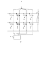
- FIG. 1 is a circuit diagram of a first embodiment of a touch sensing panel of the present invention
- FIG. 2 is a schematic diagram of a touch sensing circuit composed of a scan line, a sensing line, and a calculation circuit in the touch sensing panel of the present invention
- FIG. 3 is a waveform diagram of a scan signal emitted by a scan line in the touch sensing panel of the present invention
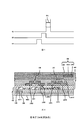
- FIG. 4 is a schematic cross-sectional view of a touch sensing panel of the present invention.
- FIG. 5 is a flowchart of a first embodiment of a touch sensing method of a touch sensing panel according to the present invention
- FIG. 6 is a flowchart of a second embodiment of a touch sensing method of a touch sensing panel according to the present invention.
- FIG. 7 is a flowchart of a method for fabricating a touch sensing panel of the present invention.
- FIG. 1 is a circuit diagram of a touch sensing panel according to a first embodiment of the present invention
- FIG. 4 is a schematic cross-sectional view of the touch sensing panel of the present invention.
- the touch sensing panel of the present embodiment includes a substrate 4011, a sensing line array layer, a dielectric layer 4012, and an organic light emitting diode display panel 402, wherein the substrate 4011, the sensing line array layer, the dielectric layer 4012, and the The organic light emitting diode display panel 402 is superimposed and integrated into one body.
- the sensing line array layer is disposed on the substrate 4011, and the sensing line array layer includes at least one sensing line 102.
- the dielectric layer 4012 is disposed on the sensing line array layer.
- the OLED display panel 402 is disposed on the dielectric layer 4012.
- the OLED display panel 402 includes a display device 106, a scan line 101, a data line 103, and a control device.
- the scan line 101 is disposed on the dielectric layer 4012, and the scan line 101 is used to provide a scan signal.
- the data line 103 is used to provide a data signal.
- the control device is coupled to the scan line 101, the data line 103, and the display device 106, and the control device is configured to control the display device 106 to display an image according to the scan signal and the data signal.
- the sensing line 102 is interleaved with the scanning line 101.
- the sensing line 102, the dielectric layer 4012 and the scanning line 101 form a sensing capacitor 104, and the sensing capacitor 104 is used in the touch.
- the touch sensing signal is generated when the touch panel is subjected to the force of the touch object.
- control device includes a first thin film transistor switch 105, a second thin film transistor switch 107, and a storage capacitor 108.
- the first thin film transistor switch 105 includes a first gate electrode 1051, a first source electrode 1052, and a first drain electrode 1053.
- the first gate 1051 is connected to the scan line 101, and the first gate 1051 is configured to receive the scan signal.
- the first source 1052 is coupled to the data line 103, and the first source 1052 is configured to receive the data signal.
- the first thin film transistor switch 105 is configured to control the opening and closing of the first current channel between the first source 1052 and the first drain 1053 according to the scan signal;
- the second thin film transistor switch 107 includes a second gate 1071, a second source 1072, and a second drain 1073.
- the second gate 1071 is connected to the first drain 1053.
- the second source 1072 is connected to the display device 106.
- the second thin film transistor switch 107 is configured to control a second current channel between the second source 1072 and the second drain 1073 according to the data signal when the first current channel is turned on. Turn it on and off.
- the second gate 1071 is connected to the first drain 1053 through a first via 4021.
- the display device 106 includes a cathode layer 1061, an organic light emitting layer 1062, and an anode layer 1063, wherein the organic light emitting layer 1062 is disposed between the cathode layer 1061 and the anode layer 1063.
- the anode layer 1063 is connected to the second drain 1073 through the second via hole 4022.
- the first plate 1081 of the storage capacitor 108 is connected to the first drain 1053, the second plate 1082 of the storage capacitor 108 is connected to the second source 1072, and the storage capacitor 108 is used for Receiving the data signal when the first current channel is turned on, and for storing a charge corresponding to the data signal, and for releasing the charge to the second gate 1071 when the first current channel is turned off a state in which the second current path is kept open.
- the display device 106 is also connected to the high potential connection terminal 109, the second drain 1073 is connected to the low potential connection terminal 110, or the display device 106 is connected to the low potential connection terminal 110.
- the second drain 1073 is connected to the high potential connection end 109.
- the thickness of the display panel having the touch sensing function can be made thinner.
- the second embodiment of the touch sensing panel of the present invention is similar to the first embodiment described above, except that:
- the touch sensing panel further includes a calculation circuit 201, the calculation circuit 201 is connected to the sensing line 102, and the calculation circuit 201 is configured to receive the touch sensing from the sensing line 102. a signal, and configured to calculate a position of the force applied by the touch object on the touch sensing panel according to the touch signal and the scan signal.
- the start times of the scan signals emitted by the adjacent two rows of scan lines 101 differ by a high level duration 301, as shown in FIG.
- FIG. 2 is a schematic diagram of a touch sensing circuit 401 composed of a scan line 101, a sensing line 102, and a computing circuit 201 in the touch sensing panel of the present invention.
- the scanning line array composed of the m scanning lines 101 is superimposed with the sensing line array composed of the n sensing lines 102 (the setting between the scanning line array and the sensing line array)
- the sensing capacitor array includes m*n sensing capacitors 104, the sensing capacitor array, and the scanning line
- the array, the sense line array, and the calculation circuit 201 constitute a touch sensing circuit 401. Where m and n are both positive integers.
- the third embodiment of the touch sensing panel of the present invention is similar to the first embodiment or the second embodiment described above, except that:
- the width of the first area in the sensing line 102 is smaller than the width of the second area, wherein the first area is an area where the sensing line 102 is interlaced with the scanning line 101,
- the second area is an area of the sensing line 102 other than the first area;
- the width of the third area in the scan line 101 is smaller than the width of the fourth area, wherein the third area is an area where the scan line 101 is interlaced with the sensing line 102, and the fourth area is the An area of the scan line 101 other than the third area.
- FIG. 5 is a flowchart of a first embodiment of a touch sensing method of a touch sensing panel according to the present invention.
- the touch sensing method of the touch sensing panel of this embodiment includes the following steps:
- control device controls the display device 106 to display an image according to the scan signal and the data signal.
- step 502 the sensing capacitor 104 formed by the sensing line 102, the dielectric layer 4012, and the scan line 101 generates the touch when the touch sensing panel receives the force of the touch object Control the sensing signal.
- FIG. 6 is a flowchart of a second embodiment of a touch sensing method of a touch sensing panel of the present invention. This embodiment is similar to the first embodiment described above, except that:
- the method further includes the following steps:
- the computing circuit 201 receives the touch sensing signal from the sensing line 102, and calculates the touch object in the touch sensing panel according to the touch signal and the scan signal. The position of the force applied on it.
- the start times of the scan signals emitted by the adjacent two rows of scan lines 101 differ by a high level duration 301, as shown in FIG.
- FIG. 7 is a flowchart of a method for fabricating a touch sensing panel of the present invention.
- the method includes the following steps:
- a first metal layer is provided on the substrate 4011.
- step 702 patterning the first metal layer to form at least one of the sensing lines 102.
- a dielectric layer 4012 is provided on the substrate 4011 and the sensing line 102.
- step 704 providing a second metal layer on the dielectric layer 4012.
- step 705 patterning the second metal layer to form at least one of the scan lines 101, wherein the scan lines 101 are interleaved with the sense lines 102, the sense lines 102, The dielectric layer 4012 and the scan line 101 form a sensing capacitor 104.
- step 706 forming the switching device, the data line 103, and the display device 106 on the dielectric layer 4012 and the scan line 101.
- step D is specifically:
- the first metal layer is provided on the substrate 4011 by sputtering or evaporation.
- the step G (step 704) is specifically:
- a second metal layer is disposed on the dielectric layer 4012 by sputtering or evaporation.
Landscapes
- Engineering & Computer Science (AREA)
- Theoretical Computer Science (AREA)
- General Engineering & Computer Science (AREA)
- Physics & Mathematics (AREA)
- General Physics & Mathematics (AREA)
- Human Computer Interaction (AREA)
- Computer Hardware Design (AREA)
- Position Input By Displaying (AREA)
- Control Of Indicators Other Than Cathode Ray Tubes (AREA)
- Electroluminescent Light Sources (AREA)
Abstract
本发明公开了一种触控感应面板及其触控感应方法、制作方法。触控感应面板包括基板、感应线阵列层、介质层和有机发光二极管显示面板;感应线与有机发光二极管显示面板的扫描线交错设置,感应线、介质层和扫描线构成的感应电容用于在触控感应面板受到作用力时生成触控感应信号。本发明能使得具有触控感应功能的显示面板更薄。
Description
本发明涉及显示技术领域,特别涉及一种触控感应面板及其触控感应方法、制作方法。
传统的触控感应面板一般同时具有图像显示功能和触控感应功能。所述图像显示功能是通过所述触控感应面板中的显示面板来实现的,所述触控感应面板是通过所述触控感应面板中的触控板或触控电路来实现的。
传统的触控感应面板实现上述功能的技术方案一般包括两种:
第一种、在所述显示面板上叠加所述触控板,即,所述显示面板和所述触控板叠加组合为一体;
第二种、在所述显示面板内部集成所述触控电路。
上述两种技术方案中的触控感应面板的厚度一般都较大,不适应触控感应面板轻薄化的趋势。
故,有必要提出一种新的技术方案,以解决上述技术问题。
本发明的目的在于提供一种触控感应面板及其触控感应方法、制作方法,其能使得具有触控感应功能的显示面板的厚度更薄。
一种触控感应面板,所述触控感应面板包括:一基板;一感应线阵列层,所述感应线阵列层设置于所述基板上,所述感应线阵列层包括:至少一感应线;一介质层,所述介质层设置于所述感应线阵列层上;以及一有机发光二极管显示面板,所述有机发光二极管显示面板设置于所述介质层上,所述有机发光二极管显示面板包括:至少一显示器件;至少一扫描线,所述扫描线设置于所述介质层上,所述扫描线用于提供扫描信号;至少一数据线,所述数据线用于提供数据信号;以及至少一控制器件,所述控制器件与所述扫描线、所述数据线和所述显示器件连接,所述控制器件用于根据所述扫描信号和所述数据信号控制所述显示器件显示图像;其中,所述感应线与所述扫描线交错设置,所述感应线、所述介质层和所述扫描线构成一感应电容,所述感应电容用于在所述触控感应面板受到触控物的作用力时生成一触控感应信号;所述触控感应面板还包括:一计算电路,所述计算电路与所述感应线连接,所述计算电路用于从所述感应线接收所述触控感应信号,并用于根据所述触控信号和所述扫描信号计算所述触控物在所述触控感应面板上所施加的所述作用力的位置;相邻两行扫描线所发出的扫描信号的起始时间相差一个高电平持续时间;所述有机发光二极管显示面板还包括:一存储电容,所述存储电容的第一极板与所述第一漏极连接,所述存储电容的第二极板与所述第二源极连接,所述存储电容用于在所述第一电流通道开启时接收所述数据信号,并用于存储与所述数据信号相应的电荷,以及用于在所述第一电流通道关闭时向所述第二栅极释放所述电荷,以使所述第二电流通道保持开启的状态。
在上述触控感应面板中,所述控制器件包括:一第一薄膜晶体管开关,所述第一薄膜晶体管开关包括:一第一栅极,所述第一栅极与所述扫描线连接,所述第一栅极用于接收所述扫描信号;一第一源极,所述第一源极与所述数据线连接,所述第一源极用于接收所述数据信号;以及一第一漏极;其中,所述第一薄膜晶体管开关用于根据所述扫描信号控制所述第一源极和所述第一漏极之间的第一电流通道的开启和关闭;一第二薄膜晶体管开关,所述第二薄膜晶体管开关包括:一第二栅极,所述第二栅极与所述第一漏极连接;一第二源极,所述第二源极与所述显示器件连接;以及一第二漏极;其中,所述第二薄膜晶体管开关用于在所述第一电流通道开启时根据所述数据信号控制所述第二源极和所述第二漏极之间的第二电流通道的开启和关闭。
在上述触控感应面板中,所述显示器件包括阴极层、有机发光层和阳极层,其中,所述有机发光层设置于所述阴极层和所述阳极层之间,所述阳极层通过第二通孔与所述第二漏极连接。
在上述触控感应面板中,所述感应线中的第一区域的宽度小于第二区域的宽度,其中,所述第一区域为所述感应线与所述扫描线交错的区域,所述第二区域为所述感应线中除所述第一区域以外的区域。
在上述触控感应面板中,所述扫描线中的第三区域的宽度小于第四区域的宽度,其中,所述第三区域为所述扫描线与所述感应线交错的区域,所述第四区域为所述扫描线中除所述第三区域以外的区域。
一种触控感应面板,所述触控感应面板包括:一基板;一感应线阵列层,所述感应线阵列层设置于所述基板上,所述感应线阵列层包括:至少一感应线;一介质层,所述介质层设置于所述感应线阵列层上;以及一有机发光二极管显示面板,所述有机发光二极管显示面板设置于所述介质层上,所述有机发光二极管显示面板包括:至少一显示器件;至少一扫描线,所述扫描线设置于所述介质层上,所述扫描线用于提供扫描信号;至少一数据线,所述数据线用于提供数据信号;以及至少一控制器件,所述控制器件与所述扫描线、所述数据线和所述显示器件连接,所述控制器件用于根据所述扫描信号和所述数据信号控制所述显示器件显示图像;其中,所述感应线与所述扫描线交错设置,所述感应线、所述介质层和所述扫描线构成一感应电容,所述感应电容用于在所述触控感应面板受到触控物的作用力时生成一触控感应信号。
在上述触控感应面板中,所述触控感应面板还包括:一计算电路,所述计算电路与所述感应线连接,所述计算电路用于从所述感应线接收所述触控感应信号,并用于根据所述触控信号和所述扫描信号计算所述触控物在所述触控感应面板上所施加的所述作用力的位置。
在上述触控感应面板中,相邻两行扫描线所发出的扫描信号的起始时间相差一个高电平持续时间。
在上述触控感应面板中,所述控制器件包括:一第一薄膜晶体管开关,所述第一薄膜晶体管开关包括:一第一栅极,所述第一栅极与所述扫描线连接,所述第一栅极用于接收所述扫描信号;一第一源极,所述第一源极与所述数据线连接,所述第一源极用于接收所述数据信号;以及一第一漏极;其中,所述第一薄膜晶体管开关用于根据所述扫描信号控制所述第一源极和所述第一漏极之间的第一电流通道的开启和关闭;一第二薄膜晶体管开关,所述第二薄膜晶体管开关包括:一第二栅极,所述第二栅极与所述第一漏极连接;一第二源极,所述第二源极与所述显示器件连接;以及一第二漏极;其中,所述第二薄膜晶体管开关用于在所述第一电流通道开启时根据所述数据信号控制所述第二源极和所述第二漏极之间的第二电流通道的开启和关闭。
在上述触控感应面板中,所述显示器件包括阴极层、有机发光层和阳极层,其中,所述有机发光层设置于所述阴极层和所述阳极层之间,所述阳极层通过第二通孔与所述第二漏极连接。
在上述触控感应面板中,所述有机发光二极管显示面板还包括:一存储电容,所述存储电容的第一极板与所述第一漏极连接,所述存储电容的第二极板与所述第二源极连接,所述存储电容用于在所述第一电流通道开启时接收所述数据信号,并用于存储与所述数据信号相应的电荷,以及用于在所述第一电流通道关闭时向所述第二栅极释放所述电荷,以使所述第二电流通道保持开启的状态。
在上述触控感应面板中,所述感应线中的第一区域的宽度小于第二区域的宽度,其中,所述第一区域为所述感应线与所述扫描线交错的区域,所述第二区域为所述感应线中除所述第一区域以外的区域。
在上述触控感应面板中,所述扫描线中的第三区域的宽度小于第四区域的宽度,其中,所述第三区域为所述扫描线与所述感应线交错的区域,所述第四区域为所述扫描线中除所述第三区域以外的区域。
在上述触控感应面板中,所述显示器件还与高电位连线端连接,所述第二漏极与低电位连线端连接。
在上述触控感应面板中,所述显示器件与所述低电位连线端连接,所述第二漏极与所述高电位连线端连接。
一种上述触控感应面板的触控感应方法,所述方法包括以下步骤:A、所述控制器件根据所述扫描信号和所述数据信号控制所述显示器件显示图像;B、由所述感应线、所述介质层和所述扫描线构成的所述感应电容在所述触控感应面板受到触控物的作用力时生成所述触控感应信号。
在上述触控感应面板的触控感应方法中,所述方法还包括以下步骤:C、所述计算电路从所述感应线接收所述触控感应信号,并根据所述触控信号和所述扫描信号计算所述触控物在所述触控感应面板上所施加的所述作用力的位置。
在上述触控感应面板的触控感应方法中,相邻两行扫描线所发出的扫描信号的起始时间相差一个高电平持续时间。
一种上述触控感应面板的制作方法,所述方法包括以下步骤:D、在所述基板上设置第一金属层;E、对所述第一金属层进行图案化处理,以形成至少一所述感应线;F、在所述基板以及所述感应线上设置介质层;G、在所述介质层上设置第二金属层;H、对所述第二金属层进行图案化处理,以形成至少一所述扫描线,其中,所述扫描线与所述感应线交错设置,所述感应线、所述介质层和所述扫描线构成一感应电容;I、在所述介质层和所述扫描线上形成所述开关器件、所述数据线和所述显示器件。
在上述触控感应面板的制作方法中,所述步骤D为:通过溅射或蒸镀的方式在所述基板上设置所述第一金属层;所述步骤G为:通过溅射或蒸镀的方式在所述介质层上设置第二金属层。
相对现有技术,本发明可以使得具有触控感应功能的显示面板的厚度更薄。
图1为本发明的触控感应面板的第一实施例的电路图;
图2为本发明的触控感应面板中由扫描线、感应线和计算电路构成的触控感应电路的示意图;
图3为本发明的触控感应面板中扫描线所发出的扫描信号的波形图;
图4为本发明的触控感应面板的截面的示意图;
图5为本发明的触控感应面板的触控感应方法的第一实施例的流程图;
图6为本发明的触控感应面板的触控感应方法的第二实施例的流程图;
图7为本发明的触控感应面板的制作方法的流程图。
本说明书所使用的词语“实施例”意指实例、示例或例证。此外,本说明书和所附权利要求中所使用的冠词“一”一般地可以被解释为“一个或多个”,除非另外指定或从上下文可以清楚确定单数形式。
参考图1和图4,图1为本发明的触控感应面板的第一实施例的电路图,图4为本发明的触控感应面板的截面的示意图。
本实施例的触控感应面板包括基板4011、感应线阵列层、介质层4012和有机发光二极管显示面板402,其中,所述基板4011、所述感应线阵列层、所述介质层4012和所述有机发光二极管显示面板402叠加组合为一体。
所述感应线阵列层设置于所述基板4011上,所述感应线阵列层包括至少一感应线102。所述介质层4012设置于所述感应线阵列层上。所述有机发光二极管显示面板402设置于所述介质层4012上,所述有机发光二极管显示面板402包括显示器件106、扫描线101、数据线103、控制器件。
所述扫描线101设置于所述介质层4012上,所述扫描线101用于提供扫描信号。所述数据线103用于提供数据信号。所述控制器件与所述扫描线101、所述数据线103和所述显示器件106连接,所述控制器件用于根据所述扫描信号和所述数据信号控制所述显示器件106显示图像。
其中,所述感应线102与所述扫描线101交错设置,所述感应线102、所述介质层4012和所述扫描线101构成一感应电容104,所述感应电容104用于在所述触控感应面板受到触控物的作用力时生成一触控感应信号。
在本实施例中,所述控制器件包括第一薄膜晶体管开关105、第二薄膜晶体管开关107和存储电容108。
所述第一薄膜晶体管开关105包括第一栅极1051、第一源极1052和第一漏极1053。所述第一栅极1051与所述扫描线101连接,所述第一栅极1051用于接收所述扫描信号。所述第一源极1052与所述数据线103连接,所述第一源极1052用于接收所述数据信号。其中,所述第一薄膜晶体管开关105用于根据所述扫描信号控制所述第一源极1052和所述第一漏极1053之间的第一电流通道的开启和关闭;
所述第二薄膜晶体管开关107包括第二栅极1071、第二源极1072以及第二漏极1073。所述第二栅极1071与所述第一漏极1053连接。所述第二源极1072与所述显示器件106连接。其中,所述第二薄膜晶体管开关107用于在所述第一电流通道开启时根据所述数据信号控制所述第二源极1072和所述第二漏极1073之间的第二电流通道的开启和关闭。所述第二栅极1071通过第一通孔4021与所述第一漏极1053连接。
所述显示器件106包括阴极层1061、有机发光层1062和阳极层1063,其中,所述有机发光层1062设置于所述阴极层1061和所述阳极层1063之间。所述阳极层1063通过第二通孔4022与所述第二漏极1073连接。
所述存储电容108的第一极板1081与所述第一漏极1053连接,所述存储电容108的第二极板1082与所述第二源极1072连接,所述存储电容108用于在所述第一电流通道开启时接收所述数据信号,并用于存储与所述数据信号相应的电荷,以及用于在所述第一电流通道关闭时向所述第二栅极1071释放所述电荷,以使所述第二电流通道保持开启的状态。
其中,所述显示器件106还与高电位连线端109连接,所述第二漏极1073与低电位连线端110连接;或者所述显示器件106与所述低电位连线端110连接,所述第二漏极1073与所述高电位连线端109连接。
在上述技术方案中,通过在显示面板中集成触控感应电路401,可以使得具有触控感应功能的显示面板的厚度更薄。
本发明的触控感应面板的第二实施例与上述第一实施例相似,不同之处在于:
在本实施例中,所述触控感应面板还包括计算电路201,所述计算电路201与所述感应线102连接,所述计算电路201用于从所述感应线102接收所述触控感应信号,并用于根据所述触控信号和所述扫描信号计算所述触控物在所述触控感应面板上所施加的所述作用力的位置。
在本实施例中,相邻两行扫描线101所发出的扫描信号的起始时间相差一个高电平持续时间301,如图3所示。
参考图2,图2为本发明的触控感应面板中由扫描线101、感应线102和计算电路201构成的触控感应电路401的示意图。从图2可以看出,在本发明中,由m条扫描线101组成的扫描线阵列与由n条感应线102组成的感应线阵列叠加为一体后(扫描线阵列和感应线阵列之间设置有所述介质层4012),所述触控感应面板中形成了m行n列的感应电容阵列,所述感应电容阵列包括m*n个感应电容104,所述感应电容阵列、所述扫描线阵列、所述感应线阵列和所述计算电路201构成触控感应电路401。其中,m和n均为正整数。
本发明的触控感应面板的第三实施例与上述第一实施例或第二实施例相似,不同之处在于:
在本实施例中,所述感应线102中的第一区域的宽度小于第二区域的宽度,其中,所述第一区域为所述感应线102与所述扫描线101交错的区域,所述第二区域为所述感应线102中除所述第一区域以外的区域;和/或
所述扫描线101中的第三区域的宽度小于第四区域的宽度,其中,所述第三区域为所述扫描线101与所述感应线102交错的区域,所述第四区域为所述扫描线101中除所述第三区域以外的区域。
这样有利于降低所述感应电容104的电容,从而提高所述触控感应面板的触控感应的精度。
参考图5,图5为本发明的触控感应面板的触控感应方法的第一实施例的流程图。本实施例的触控感应面板的触控感应方法包括以下步骤:
A(步骤501)、所述控制器件根据所述扫描信号和所述数据信号控制所述显示器件106显示图像。
B(步骤502)、由所述感应线102、所述介质层4012和所述扫描线101构成的所述感应电容104在所述触控感应面板受到触控物的作用力时生成所述触控感应信号。
图6为本发明的触控感应面板的触控感应方法的第二实施例的流程图。本实施例与上述第一实施例相似,不同之处在于:
在本实施例中,所述方法还包括以下步骤:
C(步骤601)、所述计算电路201从所述感应线102接收所述触控感应信号,并根据所述触控信号和所述扫描信号计算所述触控物在所述触控感应面板上所施加的所述作用力的位置。
在本实施例中,相邻两行扫描线101所发出的扫描信号的起始时间相差一个高电平持续时间301,如图3所示。
参考图7,图7为本发明的触控感应面板的制作方法的流程图。在本实施例中,所述方法包括以下步骤:
D(步骤701)、在所述基板4011上设置第一金属层。
E(步骤702)、对所述第一金属层进行图案化处理,以形成至少一所述感应线102。
F(步骤703)、在所述基板4011以及所述感应线102上设置介质层4012。
G(步骤704)、在所述介质层4012上设置第二金属层。
H(步骤705)、对所述第二金属层进行图案化处理,以形成至少一所述扫描线101,其中,所述扫描线101与所述感应线102交错设置,所述感应线102、所述介质层4012和所述扫描线101构成一感应电容104。
I(步骤706)、在所述介质层4012和所述扫描线101上形成所述开关器件、所述数据线103和所述显示器件106。
在本实施例中,所述步骤D(步骤701)具体为:
通过溅射或蒸镀的方式在所述基板4011上设置所述第一金属层。
所述步骤G(步骤704)具体为:
通过溅射或蒸镀的方式在所述介质层4012上设置第二金属层。
尽管已经相对于一个或多个实现方式示出并描述了本发明,但是本领域技术人员基于对本说明书和附图的阅读和理解将会想到等价变型和修改。本发明包括所有这样的修改和变型,并且仅由所附权利要求的范围限制。特别地关于由上述组件执行的各种功能,用于描述这样的组件的术语旨在对应于执行所述组件的指定功能(例如其在功能上是等价的)的任意组件(除非另外指示),即使在结构上与执行本文所示的本说明书的示范性实现方式中的功能的公开结构不等同。此外,尽管本说明书的特定特征已经相对于若干实现方式中的仅一个被公开,但是这种特征可以与如可以对给定或特定应用而言是期望和有利的其他实现方式的一个或多个其他特征组合。而且,就术语“包括”、“具有”、“含有”或其变形被用在具体实施方式或权利要求中而言,这样的术语旨在以与术语“包含”相似的方式包括。
综上所述,虽然本发明已以优选实施例揭露如上,但上述优选实施例并非用以限制本发明,本领域的普通技术人员,在不脱离本发明的精神和范围内,均可作各种更动与润饰,因此本发明的保护范围以权利要求界定的范围为准。
Claims (20)
- 一种触控感应面板,其中,所述触控感应面板包括:一基板;一感应线阵列层,所述感应线阵列层设置于所述基板上,所述感应线阵列层包括:至少一感应线;一介质层,所述介质层设置于所述感应线阵列层上;以及一有机发光二极管显示面板,所述有机发光二极管显示面板设置于所述介质层上,所述有机发光二极管显示面板包括:至少一显示器件;至少一扫描线,所述扫描线设置于所述介质层上,所述扫描线用于提供扫描信号;至少一数据线,所述数据线用于提供数据信号;以及至少一控制器件,所述控制器件与所述扫描线、所述数据线和所述显示器件连接,所述控制器件用于根据所述扫描信号和所述数据信号控制所述显示器件显示图像;其中,所述感应线与所述扫描线交错设置,所述感应线、所述介质层和所述扫描线构成一感应电容,所述感应电容用于在所述触控感应面板受到触控物的作用力时生成一触控感应信号;所述触控感应面板还包括:一计算电路,所述计算电路与所述感应线连接,所述计算电路用于从所述感应线接收所述触控感应信号,并用于根据所述触控信号和所述扫描信号计算所述触控物在所述触控感应面板上所施加的所述作用力的位置;相邻两行扫描线所发出的扫描信号的起始时间相差一个高电平持续时间;所述有机发光二极管显示面板还包括:一存储电容,所述存储电容的第一极板与所述第一漏极连接,所述存储电容的第二极板与所述第二源极连接,所述存储电容用于在所述第一电流通道开启时接收所述数据信号,并用于存储与所述数据信号相应的电荷,以及用于在所述第一电流通道关闭时向所述第二栅极释放所述电荷,以使所述第二电流通道保持开启的状态。
- 根据权利要求1所述的触控感应面板,其中,所述控制器件包括:一第一薄膜晶体管开关,所述第一薄膜晶体管开关包括:一第一栅极,所述第一栅极与所述扫描线连接,所述第一栅极用于接收所述扫描信号;一第一源极,所述第一源极与所述数据线连接,所述第一源极用于接收所述数据信号;以及一第一漏极;其中,所述第一薄膜晶体管开关用于根据所述扫描信号控制所述第一源极和所述第一漏极之间的第一电流通道的开启和关闭;一第二薄膜晶体管开关,所述第二薄膜晶体管开关包括:一第二栅极,所述第二栅极与所述第一漏极连接;一第二源极,所述第二源极与所述显示器件连接;以及一第二漏极;其中,所述第二薄膜晶体管开关用于在所述第一电流通道开启时根据所述数据信号控制所述第二源极和所述第二漏极之间的第二电流通道的开启和关闭。
- 根据权利要求2所述的触控感应面板,其中,所述显示器件包括阴极层、有机发光层和阳极层,其中,所述有机发光层设置于所述阴极层和所述阳极层之间,所述阳极层通过第二通孔与所述第二漏极连接。
- 根据权利要求1所述的触控感应面板,其中,所述感应线中的第一区域的宽度小于第二区域的宽度,其中,所述第一区域为所述感应线与所述扫描线交错的区域,所述第二区域为所述感应线中除所述第一区域以外的区域。
- 根据权利要求1所述的触控感应面板,其中,所述扫描线中的第三区域的宽度小于第四区域的宽度,其中,所述第三区域为所述扫描线与所述感应线交错的区域,所述第四区域为所述扫描线中除所述第三区域以外的区域。
- 一种触控感应面板,其中,所述触控感应面板包括:一基板;一感应线阵列层,所述感应线阵列层设置于所述基板上,所述感应线阵列层包括:至少一感应线;一介质层,所述介质层设置于所述感应线阵列层上;以及一有机发光二极管显示面板,所述有机发光二极管显示面板设置于所述介质层上,所述有机发光二极管显示面板包括:至少一显示器件;至少一扫描线,所述扫描线设置于所述介质层上,所述扫描线用于提供扫描信号;至少一数据线,所述数据线用于提供数据信号;以及至少一控制器件,所述控制器件与所述扫描线、所述数据线和所述显示器件连接,所述控制器件用于根据所述扫描信号和所述数据信号控制所述显示器件显示图像;其中,所述感应线与所述扫描线交错设置,所述感应线、所述介质层和所述扫描线构成一感应电容,所述感应电容用于在所述触控感应面板受到触控物的作用力时生成一触控感应信号。
- 根据权利要求6所述的触控感应面板,其中,所述触控感应面板还包括:一计算电路,所述计算电路与所述感应线连接,所述计算电路用于从所述感应线接收所述触控感应信号,并用于根据所述触控信号和所述扫描信号计算所述触控物在所述触控感应面板上所施加的所述作用力的位置。
- 根据权利要求6所述的触控感应面板,其中,相邻两行扫描线所发出的扫描信号的起始时间相差一个高电平持续时间。
- 根据权利要求6所述的触控感应面板,其中,所述控制器件包括:一第一薄膜晶体管开关,所述第一薄膜晶体管开关包括:一第一栅极,所述第一栅极与所述扫描线连接,所述第一栅极用于接收所述扫描信号;一第一源极,所述第一源极与所述数据线连接,所述第一源极用于接收所述数据信号;以及一第一漏极;其中,所述第一薄膜晶体管开关用于根据所述扫描信号控制所述第一源极和所述第一漏极之间的第一电流通道的开启和关闭;一第二薄膜晶体管开关,所述第二薄膜晶体管开关包括:一第二栅极,所述第二栅极与所述第一漏极连接;一第二源极,所述第二源极与所述显示器件连接;以及一第二漏极;其中,所述第二薄膜晶体管开关用于在所述第一电流通道开启时根据所述数据信号控制所述第二源极和所述第二漏极之间的第二电流通道的开启和关闭。
- 根据权利要求9所述的触控感应面板,其中,所述显示器件包括阴极层、有机发光层和阳极层,其中,所述有机发光层设置于所述阴极层和所述阳极层之间,所述阳极层通过第二通孔与所述第二漏极连接。
- 根据权利要求6所述的触控感应面板,其中,所述有机发光二极管显示面板还包括:一存储电容,所述存储电容的第一极板与所述第一漏极连接,所述存储电容的第二极板与所述第二源极连接,所述存储电容用于在所述第一电流通道开启时接收所述数据信号,并用于存储与所述数据信号相应的电荷,以及用于在所述第一电流通道关闭时向所述第二栅极释放所述电荷,以使所述第二电流通道保持开启的状态。
- 根据权利要求6所述的触控感应面板,其中,所述感应线中的第一区域的宽度小于第二区域的宽度,其中,所述第一区域为所述感应线与所述扫描线交错的区域,所述第二区域为所述感应线中除所述第一区域以外的区域。
- 根据权利要求6所述的触控感应面板,其中,所述扫描线中的第三区域的宽度小于第四区域的宽度,其中,所述第三区域为所述扫描线与所述感应线交错的区域,所述第四区域为所述扫描线中除所述第三区域以外的区域。
- 根据权利要求6所述的触控感应面板,其中,所述显示器件还与高电位连线端连接,所述第二漏极与低电位连线端连接。
- 根据权利要求6所述的触控感应面板,其中,所述显示器件与所述低电位连线端连接,所述第二漏极与所述高电位连线端连接。
- 一种如权利要求6所述的触控感应面板的触控感应方法,其中,所述方法包括以下步骤:A、所述控制器件根据所述扫描信号和所述数据信号控制所述显示器件显示图像;B、由所述感应线、所述介质层和所述扫描线构成的所述感应电容在所述触控感应面板受到触控物的作用力时生成所述触控感应信号。
- 根据权利要求16所述的触控感应面板的触控感应方法,其中,所述方法还包括以下步骤:C、所述计算电路从所述感应线接收所述触控感应信号,并根据所述触控信号和所述扫描信号计算所述触控物在所述触控感应面板上所施加的所述作用力的位置。
- 根据权利要求17所述的触控感应面板的触控感应方法,其中,相邻两行扫描线所发出的扫描信号的起始时间相差一个高电平持续时间。
- 一种如权利要求6所述的触控感应面板的制作方法,其中,所述方法包括以下步骤:D、在所述基板上设置第一金属层;E、对所述第一金属层进行图案化处理,以形成至少一所述感应线;F、在所述基板以及所述感应线上设置介质层;G、在所述介质层上设置第二金属层;H、对所述第二金属层进行图案化处理,以形成至少一所述扫描线,其中,所述扫描线与所述感应线交错设置,所述感应线、所述介质层和所述扫描线构成一感应电容;I、在所述介质层和所述扫描线上形成所述开关器件、所述数据线和所述显示器件。
- 根据权利要求19所述的触控感应面板的制作方法,其中,所述步骤D为:通过溅射或蒸镀的方式在所述基板上设置所述第一金属层;所述步骤G为:通过溅射或蒸镀的方式在所述介质层上设置第二金属层。
Priority Applications (1)
| Application Number | Priority Date | Filing Date | Title |
|---|---|---|---|
| US14/781,043 US9880657B2 (en) | 2015-04-13 | 2015-04-30 | Touch-sensitive panel, method, and method of manufacturing the same |
Applications Claiming Priority (2)
| Application Number | Priority Date | Filing Date | Title |
|---|---|---|---|
| CN201510171004.0A CN104777935B (zh) | 2015-04-13 | 2015-04-13 | 触控感应面板及其触控感应方法、制作方法 |
| CN201510171004.0 | 2015-04-13 |
Publications (1)
| Publication Number | Publication Date |
|---|---|
| WO2016165170A1 true WO2016165170A1 (zh) | 2016-10-20 |
Family
ID=53619445
Family Applications (1)
| Application Number | Title | Priority Date | Filing Date |
|---|---|---|---|
| PCT/CN2015/078081 Ceased WO2016165170A1 (zh) | 2015-04-13 | 2015-04-30 | 触控感应面板及其触控感应方法、制作方法 |
Country Status (3)
| Country | Link |
|---|---|
| US (1) | US9880657B2 (zh) |
| CN (1) | CN104777935B (zh) |
| WO (1) | WO2016165170A1 (zh) |
Families Citing this family (6)
| Publication number | Priority date | Publication date | Assignee | Title |
|---|---|---|---|---|
| CN107704136B (zh) * | 2017-10-23 | 2020-04-14 | 京东方科技集团股份有限公司 | 一种有机电致发光显示面板、其触控检测方法及显示装置 |
| CN109375839B (zh) * | 2018-12-03 | 2020-06-30 | 武汉华星光电半导体显示技术有限公司 | 一种触控屏、显示装置 |
| CN109407893B (zh) * | 2018-12-17 | 2021-01-01 | 武汉华星光电半导体显示技术有限公司 | 触控显示面板及其制作方法 |
| US11188178B2 (en) | 2018-12-17 | 2021-11-30 | Wuhan China Star Optofi Fctronics Semiconductor Display Technology Co., Ltd. | Touch display panel, manufacturing method thereof, and touch display device |
| EP4088550A4 (en) * | 2020-01-07 | 2024-01-10 | Ghsp, Inc. | INDUCTIVE HOB DISPLAY |
| CN111696494A (zh) * | 2020-07-02 | 2020-09-22 | Tcl华星光电技术有限公司 | 显示面板及显示装置 |
Citations (4)
| Publication number | Priority date | Publication date | Assignee | Title |
|---|---|---|---|---|
| US20110090174A1 (en) * | 2009-10-16 | 2011-04-21 | Aussmak Optoelectronics Corp. | Driving method of touch display module |
| CN103927988A (zh) * | 2014-04-03 | 2014-07-16 | 深圳市华星光电技术有限公司 | 一种oled显示器的阵列基板 |
| CN104076993A (zh) * | 2013-03-29 | 2014-10-01 | 北京京东方光电科技有限公司 | 一种触控显示面板、触摸定位方法和显示装置 |
| CN104393025A (zh) * | 2014-12-09 | 2015-03-04 | 京东方科技集团股份有限公司 | 一种阵列基板、触控显示面板和触控显示装置 |
Family Cites Families (5)
| Publication number | Priority date | Publication date | Assignee | Title |
|---|---|---|---|---|
| TW523627B (en) * | 1998-07-14 | 2003-03-11 | Hitachi Ltd | Liquid crystal display device |
| JP2002215063A (ja) * | 2001-01-19 | 2002-07-31 | Sony Corp | アクティブマトリクス型表示装置 |
| JP3743505B2 (ja) * | 2001-06-15 | 2006-02-08 | セイコーエプソン株式会社 | ライン駆動回路、電気光学装置及び表示装置 |
| CN101598871B (zh) * | 2008-06-04 | 2011-09-28 | 群康科技(深圳)有限公司 | 触控液晶显示装置及其驱动方法 |
| CN104298404B (zh) * | 2014-10-28 | 2017-05-31 | 上海天马微电子有限公司 | 阵列基板及其制作方法、显示装置及其驱动方法 |
-
2015
- 2015-04-13 CN CN201510171004.0A patent/CN104777935B/zh active Active
- 2015-04-30 US US14/781,043 patent/US9880657B2/en active Active
- 2015-04-30 WO PCT/CN2015/078081 patent/WO2016165170A1/zh not_active Ceased
Patent Citations (4)
| Publication number | Priority date | Publication date | Assignee | Title |
|---|---|---|---|---|
| US20110090174A1 (en) * | 2009-10-16 | 2011-04-21 | Aussmak Optoelectronics Corp. | Driving method of touch display module |
| CN104076993A (zh) * | 2013-03-29 | 2014-10-01 | 北京京东方光电科技有限公司 | 一种触控显示面板、触摸定位方法和显示装置 |
| CN103927988A (zh) * | 2014-04-03 | 2014-07-16 | 深圳市华星光电技术有限公司 | 一种oled显示器的阵列基板 |
| CN104393025A (zh) * | 2014-12-09 | 2015-03-04 | 京东方科技集团股份有限公司 | 一种阵列基板、触控显示面板和触控显示装置 |
Also Published As
| Publication number | Publication date |
|---|---|
| CN104777935B (zh) | 2017-09-19 |
| US20170139519A1 (en) | 2017-05-18 |
| US9880657B2 (en) | 2018-01-30 |
| CN104777935A (zh) | 2015-07-15 |
Similar Documents
| Publication | Publication Date | Title |
|---|---|---|
| WO2016165170A1 (zh) | 触控感应面板及其触控感应方法、制作方法 | |
| WO2016165167A1 (zh) | 感应面板及其制作方法、感应压力和温度的方法 | |
| WO2018188135A1 (zh) | 一种像素补偿电路及显示装置 | |
| WO2019114062A1 (zh) | Oled 显示面板及显示装置 | |
| WO2017049688A1 (zh) | 一种goa电路及其驱动方法、液晶显示器 | |
| WO2016101293A1 (zh) | 驱动电路 | |
| WO2019075813A1 (zh) | 微型led显示面板及微型led显示器 | |
| CN108563352A (zh) | 一种触控显示基板、制作方法、触控显示装置及驱动方法 | |
| WO2016106797A1 (zh) | 一种柔性有机发光显示器及其制作方法 | |
| WO2019019503A1 (zh) | 一种像素补偿电路 | |
| WO2016078204A1 (zh) | 一种液晶显示面板及阵列基板 | |
| WO2017045220A1 (zh) | 一种goa电路及液晶显示器 | |
| WO2016074262A1 (zh) | 一种coa阵列基板及液晶显示面板 | |
| WO2016008184A1 (zh) | 一种显示面板及显示装置 | |
| WO2016000296A1 (zh) | 低色偏液晶阵列基板及其驱动方法 | |
| WO2019037224A1 (zh) | 显示屏及其制备方法 | |
| WO2016095243A1 (zh) | 液晶面板及其制备方法 | |
| WO2018035894A1 (zh) | 像素结构及制作方法 | |
| TW202021111A (zh) | 具有垂直結構的電晶體及電子裝置 | |
| WO2016078112A1 (zh) | 薄膜晶体管基板的制作方法及制造设备 | |
| WO2018094815A1 (zh) | Oled器件的制作方法及oled器件 | |
| WO2017128597A1 (zh) | 液晶显示面板、tft基板及其制造方法 | |
| WO2017016042A1 (zh) | 有机薄膜晶体管阵列基板及其制作方法 | |
| WO2017071054A1 (zh) | 一种显示面板及其制造方法 | |
| WO2017041316A1 (zh) | 显示面板 |
Legal Events
| Date | Code | Title | Description |
|---|---|---|---|
| WWE | Wipo information: entry into national phase |
Ref document number: 14781043 Country of ref document: US |
|
| 121 | Ep: the epo has been informed by wipo that ep was designated in this application |
Ref document number: 15888874 Country of ref document: EP Kind code of ref document: A1 |
|
| NENP | Non-entry into the national phase |
Ref country code: DE |
|
| 122 | Ep: pct application non-entry in european phase |
Ref document number: 15888874 Country of ref document: EP Kind code of ref document: A1 |