WO2016163525A1 - 高分子化合物、表面処理剤、表面処理剤を用いた積層体、トランジスタ、積層体の製造方法 - Google Patents
高分子化合物、表面処理剤、表面処理剤を用いた積層体、トランジスタ、積層体の製造方法 Download PDFInfo
- Publication number
- WO2016163525A1 WO2016163525A1 PCT/JP2016/061571 JP2016061571W WO2016163525A1 WO 2016163525 A1 WO2016163525 A1 WO 2016163525A1 JP 2016061571 W JP2016061571 W JP 2016061571W WO 2016163525 A1 WO2016163525 A1 WO 2016163525A1
- Authority
- WO
- WIPO (PCT)
- Prior art keywords
- group
- formula
- represented
- polymer compound
- following formula
- Prior art date
- Legal status (The legal status is an assumption and is not a legal conclusion. Google has not performed a legal analysis and makes no representation as to the accuracy of the status listed.)
- Ceased
Links
- 0 CC(OC(*)c(c(*)c(*)c(*)c1)c1[N+]([O-])=O)=O Chemical compound CC(OC(*)c(c(*)c(*)c(*)c1)c1[N+]([O-])=O)=O 0.000 description 3
Images


Classifications
-
- C—CHEMISTRY; METALLURGY
- C09—DYES; PAINTS; POLISHES; NATURAL RESINS; ADHESIVES; COMPOSITIONS NOT OTHERWISE PROVIDED FOR; APPLICATIONS OF MATERIALS NOT OTHERWISE PROVIDED FOR
- C09D—COATING COMPOSITIONS, e.g. PAINTS, VARNISHES OR LACQUERS; FILLING PASTES; CHEMICAL PAINT OR INK REMOVERS; INKS; CORRECTING FLUIDS; WOODSTAINS; PASTES OR SOLIDS FOR COLOURING OR PRINTING; USE OF MATERIALS THEREFOR
- C09D133/00—Coating compositions based on homopolymers or copolymers of compounds having one or more unsaturated aliphatic radicals, each having only one carbon-to-carbon double bond, and at least one being terminated by only one carboxyl radical, or of salts, anhydrides, esters, amides, imides, or nitriles thereof; Coating compositions based on derivatives of such polymers
- C09D133/04—Homopolymers or copolymers of esters
- C09D133/14—Homopolymers or copolymers of esters of esters containing halogen, nitrogen, sulfur or oxygen atoms in addition to the carboxy oxygen
-
- C—CHEMISTRY; METALLURGY
- C08—ORGANIC MACROMOLECULAR COMPOUNDS; THEIR PREPARATION OR CHEMICAL WORKING-UP; COMPOSITIONS BASED THEREON
- C08F—MACROMOLECULAR COMPOUNDS OBTAINED BY REACTIONS ONLY INVOLVING CARBON-TO-CARBON UNSATURATED BONDS
- C08F120/00—Homopolymers of compounds having one or more unsaturated aliphatic radicals, each having only one carbon-to-carbon double bond, and only one being terminated by only one carboxyl radical or a salt, anhydride, ester, amide, imide or nitrile thereof
- C08F120/02—Monocarboxylic acids having less than ten carbon atoms; Derivatives thereof
- C08F120/10—Esters
- C08F120/34—Esters containing nitrogen, e.g. N,N-dimethylaminoethyl (meth)acrylate
- C08F120/36—Esters containing nitrogen, e.g. N,N-dimethylaminoethyl (meth)acrylate containing oxygen in addition to the carboxy oxygen, e.g. 2-N-morpholinoethyl (meth)acrylate or 2-isocyanatoethyl (meth)acrylate
-
- C—CHEMISTRY; METALLURGY
- C08—ORGANIC MACROMOLECULAR COMPOUNDS; THEIR PREPARATION OR CHEMICAL WORKING-UP; COMPOSITIONS BASED THEREON
- C08F—MACROMOLECULAR COMPOUNDS OBTAINED BY REACTIONS ONLY INVOLVING CARBON-TO-CARBON UNSATURATED BONDS
- C08F20/00—Homopolymers and copolymers of compounds having one or more unsaturated aliphatic radicals, each having only one carbon-to-carbon double bond, and only one being terminated by only one carboxyl radical or a salt, anhydride, ester, amide, imide or nitrile thereof
- C08F20/02—Monocarboxylic acids having less than ten carbon atoms, Derivatives thereof
- C08F20/04—Acids, Metal salts or ammonium salts thereof
- C08F20/06—Acrylic acid; Methacrylic acid; Metal salts or ammonium salts thereof
-
- C—CHEMISTRY; METALLURGY
- C08—ORGANIC MACROMOLECULAR COMPOUNDS; THEIR PREPARATION OR CHEMICAL WORKING-UP; COMPOSITIONS BASED THEREON
- C08F—MACROMOLECULAR COMPOUNDS OBTAINED BY REACTIONS ONLY INVOLVING CARBON-TO-CARBON UNSATURATED BONDS
- C08F20/00—Homopolymers and copolymers of compounds having one or more unsaturated aliphatic radicals, each having only one carbon-to-carbon double bond, and only one being terminated by only one carboxyl radical or a salt, anhydride, ester, amide, imide or nitrile thereof
- C08F20/02—Monocarboxylic acids having less than ten carbon atoms, Derivatives thereof
- C08F20/10—Esters
- C08F20/34—Esters containing nitrogen, e.g. N,N-dimethylaminoethyl (meth)acrylate
- C08F20/36—Esters containing nitrogen, e.g. N,N-dimethylaminoethyl (meth)acrylate containing oxygen in addition to the carboxy oxygen, e.g. 2-N-morpholinoethyl (meth)acrylate or 2-isocyanatoethyl (meth)acrylate
-
- C—CHEMISTRY; METALLURGY
- C23—COATING METALLIC MATERIAL; COATING MATERIAL WITH METALLIC MATERIAL; CHEMICAL SURFACE TREATMENT; DIFFUSION TREATMENT OF METALLIC MATERIAL; COATING BY VACUUM EVAPORATION, BY SPUTTERING, BY ION IMPLANTATION OR BY CHEMICAL VAPOUR DEPOSITION, IN GENERAL; INHIBITING CORROSION OF METALLIC MATERIAL OR INCRUSTATION IN GENERAL
- C23C—COATING METALLIC MATERIAL; COATING MATERIAL WITH METALLIC MATERIAL; SURFACE TREATMENT OF METALLIC MATERIAL BY DIFFUSION INTO THE SURFACE, BY CHEMICAL CONVERSION OR SUBSTITUTION; COATING BY VACUUM EVAPORATION, BY SPUTTERING, BY ION IMPLANTATION OR BY CHEMICAL VAPOUR DEPOSITION, IN GENERAL
- C23C18/00—Chemical coating by decomposition of either liquid compounds or solutions of the coating forming compounds, without leaving reaction products of surface material in the coating; Contact plating
- C23C18/16—Chemical coating by decomposition of either liquid compounds or solutions of the coating forming compounds, without leaving reaction products of surface material in the coating; Contact plating by reduction or substitution, e.g. electroless plating
- C23C18/1601—Process or apparatus
- C23C18/1603—Process or apparatus coating on selected surface areas
- C23C18/1607—Process or apparatus coating on selected surface areas by direct patterning
- C23C18/1608—Process or apparatus coating on selected surface areas by direct patterning from pretreatment step, i.e. selective pre-treatment
-
- C—CHEMISTRY; METALLURGY
- C23—COATING METALLIC MATERIAL; COATING MATERIAL WITH METALLIC MATERIAL; CHEMICAL SURFACE TREATMENT; DIFFUSION TREATMENT OF METALLIC MATERIAL; COATING BY VACUUM EVAPORATION, BY SPUTTERING, BY ION IMPLANTATION OR BY CHEMICAL VAPOUR DEPOSITION, IN GENERAL; INHIBITING CORROSION OF METALLIC MATERIAL OR INCRUSTATION IN GENERAL
- C23C—COATING METALLIC MATERIAL; COATING MATERIAL WITH METALLIC MATERIAL; SURFACE TREATMENT OF METALLIC MATERIAL BY DIFFUSION INTO THE SURFACE, BY CHEMICAL CONVERSION OR SUBSTITUTION; COATING BY VACUUM EVAPORATION, BY SPUTTERING, BY ION IMPLANTATION OR BY CHEMICAL VAPOUR DEPOSITION, IN GENERAL
- C23C18/00—Chemical coating by decomposition of either liquid compounds or solutions of the coating forming compounds, without leaving reaction products of surface material in the coating; Contact plating
- C23C18/16—Chemical coating by decomposition of either liquid compounds or solutions of the coating forming compounds, without leaving reaction products of surface material in the coating; Contact plating by reduction or substitution, e.g. electroless plating
- C23C18/1601—Process or apparatus
- C23C18/1603—Process or apparatus coating on selected surface areas
- C23C18/1607—Process or apparatus coating on selected surface areas by direct patterning
- C23C18/1612—Process or apparatus coating on selected surface areas by direct patterning through irradiation means
-
- C—CHEMISTRY; METALLURGY
- C23—COATING METALLIC MATERIAL; COATING MATERIAL WITH METALLIC MATERIAL; CHEMICAL SURFACE TREATMENT; DIFFUSION TREATMENT OF METALLIC MATERIAL; COATING BY VACUUM EVAPORATION, BY SPUTTERING, BY ION IMPLANTATION OR BY CHEMICAL VAPOUR DEPOSITION, IN GENERAL; INHIBITING CORROSION OF METALLIC MATERIAL OR INCRUSTATION IN GENERAL
- C23C—COATING METALLIC MATERIAL; COATING MATERIAL WITH METALLIC MATERIAL; SURFACE TREATMENT OF METALLIC MATERIAL BY DIFFUSION INTO THE SURFACE, BY CHEMICAL CONVERSION OR SUBSTITUTION; COATING BY VACUUM EVAPORATION, BY SPUTTERING, BY ION IMPLANTATION OR BY CHEMICAL VAPOUR DEPOSITION, IN GENERAL
- C23C18/00—Chemical coating by decomposition of either liquid compounds or solutions of the coating forming compounds, without leaving reaction products of surface material in the coating; Contact plating
- C23C18/16—Chemical coating by decomposition of either liquid compounds or solutions of the coating forming compounds, without leaving reaction products of surface material in the coating; Contact plating by reduction or substitution, e.g. electroless plating
- C23C18/18—Pretreatment of the material to be coated
- C23C18/20—Pretreatment of the material to be coated of organic surfaces, e.g. resins
-
- C—CHEMISTRY; METALLURGY
- C23—COATING METALLIC MATERIAL; COATING MATERIAL WITH METALLIC MATERIAL; CHEMICAL SURFACE TREATMENT; DIFFUSION TREATMENT OF METALLIC MATERIAL; COATING BY VACUUM EVAPORATION, BY SPUTTERING, BY ION IMPLANTATION OR BY CHEMICAL VAPOUR DEPOSITION, IN GENERAL; INHIBITING CORROSION OF METALLIC MATERIAL OR INCRUSTATION IN GENERAL
- C23C—COATING METALLIC MATERIAL; COATING MATERIAL WITH METALLIC MATERIAL; SURFACE TREATMENT OF METALLIC MATERIAL BY DIFFUSION INTO THE SURFACE, BY CHEMICAL CONVERSION OR SUBSTITUTION; COATING BY VACUUM EVAPORATION, BY SPUTTERING, BY ION IMPLANTATION OR BY CHEMICAL VAPOUR DEPOSITION, IN GENERAL
- C23C18/00—Chemical coating by decomposition of either liquid compounds or solutions of the coating forming compounds, without leaving reaction products of surface material in the coating; Contact plating
- C23C18/16—Chemical coating by decomposition of either liquid compounds or solutions of the coating forming compounds, without leaving reaction products of surface material in the coating; Contact plating by reduction or substitution, e.g. electroless plating
- C23C18/18—Pretreatment of the material to be coated
- C23C18/20—Pretreatment of the material to be coated of organic surfaces, e.g. resins
- C23C18/2006—Pretreatment of the material to be coated of organic surfaces, e.g. resins by other methods than those of C23C18/22 - C23C18/30
- C23C18/2026—Pretreatment of the material to be coated of organic surfaces, e.g. resins by other methods than those of C23C18/22 - C23C18/30 by radiant energy
-
- C—CHEMISTRY; METALLURGY
- C23—COATING METALLIC MATERIAL; COATING MATERIAL WITH METALLIC MATERIAL; CHEMICAL SURFACE TREATMENT; DIFFUSION TREATMENT OF METALLIC MATERIAL; COATING BY VACUUM EVAPORATION, BY SPUTTERING, BY ION IMPLANTATION OR BY CHEMICAL VAPOUR DEPOSITION, IN GENERAL; INHIBITING CORROSION OF METALLIC MATERIAL OR INCRUSTATION IN GENERAL
- C23C—COATING METALLIC MATERIAL; COATING MATERIAL WITH METALLIC MATERIAL; SURFACE TREATMENT OF METALLIC MATERIAL BY DIFFUSION INTO THE SURFACE, BY CHEMICAL CONVERSION OR SUBSTITUTION; COATING BY VACUUM EVAPORATION, BY SPUTTERING, BY ION IMPLANTATION OR BY CHEMICAL VAPOUR DEPOSITION, IN GENERAL
- C23C18/00—Chemical coating by decomposition of either liquid compounds or solutions of the coating forming compounds, without leaving reaction products of surface material in the coating; Contact plating
- C23C18/16—Chemical coating by decomposition of either liquid compounds or solutions of the coating forming compounds, without leaving reaction products of surface material in the coating; Contact plating by reduction or substitution, e.g. electroless plating
- C23C18/18—Pretreatment of the material to be coated
- C23C18/20—Pretreatment of the material to be coated of organic surfaces, e.g. resins
- C23C18/2006—Pretreatment of the material to be coated of organic surfaces, e.g. resins by other methods than those of C23C18/22 - C23C18/30
- C23C18/2046—Pretreatment of the material to be coated of organic surfaces, e.g. resins by other methods than those of C23C18/22 - C23C18/30 by chemical pretreatment
- C23C18/2053—Pretreatment of the material to be coated of organic surfaces, e.g. resins by other methods than those of C23C18/22 - C23C18/30 by chemical pretreatment only one step pretreatment
- C23C18/2066—Use of organic or inorganic compounds other than metals, e.g. activation, sensitisation with polymers
-
- C—CHEMISTRY; METALLURGY
- C23—COATING METALLIC MATERIAL; COATING MATERIAL WITH METALLIC MATERIAL; CHEMICAL SURFACE TREATMENT; DIFFUSION TREATMENT OF METALLIC MATERIAL; COATING BY VACUUM EVAPORATION, BY SPUTTERING, BY ION IMPLANTATION OR BY CHEMICAL VAPOUR DEPOSITION, IN GENERAL; INHIBITING CORROSION OF METALLIC MATERIAL OR INCRUSTATION IN GENERAL
- C23C—COATING METALLIC MATERIAL; COATING MATERIAL WITH METALLIC MATERIAL; SURFACE TREATMENT OF METALLIC MATERIAL BY DIFFUSION INTO THE SURFACE, BY CHEMICAL CONVERSION OR SUBSTITUTION; COATING BY VACUUM EVAPORATION, BY SPUTTERING, BY ION IMPLANTATION OR BY CHEMICAL VAPOUR DEPOSITION, IN GENERAL
- C23C18/00—Chemical coating by decomposition of either liquid compounds or solutions of the coating forming compounds, without leaving reaction products of surface material in the coating; Contact plating
- C23C18/16—Chemical coating by decomposition of either liquid compounds or solutions of the coating forming compounds, without leaving reaction products of surface material in the coating; Contact plating by reduction or substitution, e.g. electroless plating
- C23C18/18—Pretreatment of the material to be coated
- C23C18/20—Pretreatment of the material to be coated of organic surfaces, e.g. resins
- C23C18/28—Sensitising or activating
- C23C18/30—Activating or accelerating or sensitising with palladium or other noble metal
-
- H—ELECTRICITY
- H05—ELECTRIC TECHNIQUES NOT OTHERWISE PROVIDED FOR
- H05K—PRINTED CIRCUITS; CASINGS OR CONSTRUCTIONAL DETAILS OF ELECTRIC APPARATUS; MANUFACTURE OF ASSEMBLAGES OF ELECTRICAL COMPONENTS
- H05K3/00—Apparatus or processes for manufacturing printed circuits
- H05K3/10—Apparatus or processes for manufacturing printed circuits in which conductive material is applied to the insulating support in such a manner as to form the desired conductive pattern
- H05K3/18—Apparatus or processes for manufacturing printed circuits in which conductive material is applied to the insulating support in such a manner as to form the desired conductive pattern using precipitation techniques to apply the conductive material
-
- H—ELECTRICITY
- H05—ELECTRIC TECHNIQUES NOT OTHERWISE PROVIDED FOR
- H05K—PRINTED CIRCUITS; CASINGS OR CONSTRUCTIONAL DETAILS OF ELECTRIC APPARATUS; MANUFACTURE OF ASSEMBLAGES OF ELECTRICAL COMPONENTS
- H05K3/00—Apparatus or processes for manufacturing printed circuits
- H05K3/10—Apparatus or processes for manufacturing printed circuits in which conductive material is applied to the insulating support in such a manner as to form the desired conductive pattern
- H05K3/18—Apparatus or processes for manufacturing printed circuits in which conductive material is applied to the insulating support in such a manner as to form the desired conductive pattern using precipitation techniques to apply the conductive material
- H05K3/181—Apparatus or processes for manufacturing printed circuits in which conductive material is applied to the insulating support in such a manner as to form the desired conductive pattern using precipitation techniques to apply the conductive material by electroless plating
-
- H—ELECTRICITY
- H05—ELECTRIC TECHNIQUES NOT OTHERWISE PROVIDED FOR
- H05K—PRINTED CIRCUITS; CASINGS OR CONSTRUCTIONAL DETAILS OF ELECTRIC APPARATUS; MANUFACTURE OF ASSEMBLAGES OF ELECTRICAL COMPONENTS
- H05K3/00—Apparatus or processes for manufacturing printed circuits
- H05K3/38—Improvement of the adhesion between the insulating substrate and the metal
-
- H—ELECTRICITY
- H05—ELECTRIC TECHNIQUES NOT OTHERWISE PROVIDED FOR
- H05K—PRINTED CIRCUITS; CASINGS OR CONSTRUCTIONAL DETAILS OF ELECTRIC APPARATUS; MANUFACTURE OF ASSEMBLAGES OF ELECTRICAL COMPONENTS
- H05K3/00—Apparatus or processes for manufacturing printed circuits
- H05K3/38—Improvement of the adhesion between the insulating substrate and the metal
- H05K3/386—Improvement of the adhesion between the insulating substrate and the metal by the use of an organic polymeric bonding layer, e.g. adhesive
- H05K3/387—Improvement of the adhesion between the insulating substrate and the metal by the use of an organic polymeric bonding layer, e.g. adhesive for electroless plating
-
- C—CHEMISTRY; METALLURGY
- C08—ORGANIC MACROMOLECULAR COMPOUNDS; THEIR PREPARATION OR CHEMICAL WORKING-UP; COMPOSITIONS BASED THEREON
- C08F—MACROMOLECULAR COMPOUNDS OBTAINED BY REACTIONS ONLY INVOLVING CARBON-TO-CARBON UNSATURATED BONDS
- C08F2438/00—Living radical polymerisation
- C08F2438/01—Atom Transfer Radical Polymerization [ATRP] or reverse ATRP
-
- C—CHEMISTRY; METALLURGY
- C23—COATING METALLIC MATERIAL; COATING MATERIAL WITH METALLIC MATERIAL; CHEMICAL SURFACE TREATMENT; DIFFUSION TREATMENT OF METALLIC MATERIAL; COATING BY VACUUM EVAPORATION, BY SPUTTERING, BY ION IMPLANTATION OR BY CHEMICAL VAPOUR DEPOSITION, IN GENERAL; INHIBITING CORROSION OF METALLIC MATERIAL OR INCRUSTATION IN GENERAL
- C23C—COATING METALLIC MATERIAL; COATING MATERIAL WITH METALLIC MATERIAL; SURFACE TREATMENT OF METALLIC MATERIAL BY DIFFUSION INTO THE SURFACE, BY CHEMICAL CONVERSION OR SUBSTITUTION; COATING BY VACUUM EVAPORATION, BY SPUTTERING, BY ION IMPLANTATION OR BY CHEMICAL VAPOUR DEPOSITION, IN GENERAL
- C23C18/00—Chemical coating by decomposition of either liquid compounds or solutions of the coating forming compounds, without leaving reaction products of surface material in the coating; Contact plating
- C23C18/16—Chemical coating by decomposition of either liquid compounds or solutions of the coating forming compounds, without leaving reaction products of surface material in the coating; Contact plating by reduction or substitution, e.g. electroless plating
- C23C18/31—Coating with metals
- C23C18/32—Coating with nickel, cobalt or mixtures thereof with phosphorus or boron
- C23C18/34—Coating with nickel, cobalt or mixtures thereof with phosphorus or boron using reducing agents
- C23C18/36—Coating with nickel, cobalt or mixtures thereof with phosphorus or boron using reducing agents using hypophosphites
Definitions
- the present invention relates to a compound used for electroless plating formation.
- the present invention claims the priority of Japanese Patent Application No. 2015-81164 filed on April 10, 2015, and for the designated countries where weaving by reference of documents is permitted, the contents described in the application are as follows: Is incorporated into this application by reference.
- Patent Document 1 discloses that a resin substrate surface is irradiated with excimer light in a desired pattern, and then a silane coupling agent having an amino group or amino-modified. A resin substrate is brought into contact with the reactive silicon oil formed, and a receiving layer for capturing and immobilizing a catalyst for initiating the electroless plating reaction is formed in the excimer light irradiation part, and nickel is formed on the receiving layer. A method for forming a phosphorous plating layer by electroless plating is described.
- the conventional silane coupling agent used as a material for capturing a catalyst for electroless plating has a high reactivity of an alkoxysilyl group or a halogenated silyl group contained in the molecule, so that moisture and solvent in the atmosphere. It is known that the aging stability is low such that the condensation reaction proceeds due to hydrolysis by moisture contained in the water, and siloxane is produced. As a result of such a reaction, agglomeration, suspension and sedimentation tend to progress and the film formability tends to decrease.
- This invention is made
- the present inventors searched for a compound that can be used as a material having excellent stability and adhesion to a substrate. As a result, the present inventors have found a group of compounds that can be substituted for the silane coupling agent, and have completed the present invention.
- the present application includes a plurality of means for solving at least a part of the above-described problems, and examples thereof are as follows.
- the first aspect of the present invention for solving the above problems is a polymer compound having a structural unit represented by the following formula (1).
- R 1 represents hydrogen or a methyl group
- m represents an integer of 2 to 20
- Q represents a photosensitive leaving group
- the second aspect of the present invention is a polymer compound, wherein Q is at least one group represented by the following formula (2).
- R 2 represents hydrogen or an alkyl group
- R 3 and R 4 each independently represents an alkyl group or a fluoroalkyl group containing a methyl group
- R 5 represents hydrogen or a nitro group.
- a method for producing a laminate the step of applying a surface treatment agent containing the polymer compound to form a photosensitive polymer layer, and forming the photosensitive polymer layer in a predetermined pattern.
- a method for producing a laminate having:
- (meth) acrylate means acrylate and / or methacrylate.
- the polymer compound according to the present embodiment includes at least one structural unit represented by the following formula (1).
- R 1 represents hydrogen or a methyl group
- m represents an integer of 2 to 20. Of these, those represented by integers from 2 to 16 are preferred, and those represented by integers from 2 to 8 are particularly preferred.
- Q represents a photosensitive leaving group.
- the photosensitive leaving group is an amine protecting group present in the structural unit, and generates an amine in response to light, and the structure is not limited as long as it has a property of not capturing a metal.
- Q is at least one group represented by the following formula (2).
- R 2 represents hydrogen or a linear, branched or cyclic alkyl group having 1 to 10 carbon atoms.
- the alkyl group having 1 to 10 carbon atoms include a methyl group, an ethyl group, an n-propyl group, an isopropyl group, an n-butyl group, a t-butyl group, and a cyclohexyl group.
- isopropyl, ethyl and methyl are preferable, and isopropyl and methyl are particularly preferable.
- R 3 and R 4 each independently represents a linear or branched alkyl group having 1 to 30 carbon atoms or a linear or branched fluoroalkyl group having 1 to 30 carbon atoms.
- the alkyl group having 1 to 30 carbon atoms include a methyl group, an ethyl group, an n-propyl group, an isopropyl group, an n-butyl group, a t-butyl group, and a decyl group.
- a chain alkyl group is preferred, and a methyl group is particularly preferred.
- fluoroalkyl group having 1 to 30 carbon atoms include a trifluoromethyl group, a pentafluoroethyl group, a heptafluoropropyl group, and 1- (trifluoromethyl) -1,2,2,2-tetrafluoro.
- a fluorooctyl group, a heptadecafluoroundecyl group, a tridecafluorononyl group, a trifluorodecyl group, and the like can be mentioned. It is a fluoroundecyl group.
- R 3 and R 4 can be independently selected, and may be the same substituent or different substituents.
- R 5 represents hydrogen or a nitro group.
- the polymer compound represented by the formula (1) in which Q is a group represented by the formula (2) is obtained, for example, by polymerizing a compound (monomer) represented by the following formula (3). It is expressed as equation (4).
- R 1 to R 5 and m represent the same meaning as described above.
- the polymerization of the compound represented by the formula (3) is not particularly limited, but radical polymerization is preferable from the viewpoint of ease of control and the like, and among radical polymerization, controlled radical polymerization is more preferable.
- the controlled radical polymerization method include a chain transfer agent method, a living radical polymerization method that is a kind of living polymerization, and the like, and living radical polymerization that can easily control the molecular weight distribution is more preferable.
- Living radical polymerization methods include nitroxy radical polymerization method (NMP), atom transfer radical polymerization method (ATRP), reversible addition fragmentation chain transfer method (RAFT), etc., from the viewpoint of temperature and versatility. In particular, the atom transfer radical polymerization method (ATRP) is desirable.
- radical polymerization when using radical polymerization, a conventionally well-known polymerization initiator can be used suitably.
- the radical polymerization initiator may be used alone or in combination of two or more thereof, or commercially available ones may be used as they are.
- an azo polymerization initiator that has an azo group (—N ⁇ N—) and generates a radical with N 2 can be used.
- Specific examples include azonitrile, azoester, azoamide, azoamidine, azoimidazoline and the like.
- 2,2′-azobis (2-amidinopropane) dihydrochloride 4,4′-azobis (4-cyanovaleric acid), 2,2′-bis (2-imidazoline- 2-yl) -2,2′-azopropanedihydrochloride, 2,2′-bis (2-imidazolin-2-yl) -2,2′-azopropane, 2,2′-azobis [N- (2 -Hydroxyethyl) -2-methylpropionamide], 2,2′-azobisisobutyronitrile (AIBN), 2,2′-azobis (2,4-dimethylvaleronitrile) (ADBN).
- AIBN 2,2′-azobisisobutyronitrile
- ADBN 2,2′-azobis (2,4-dimethylvaleronitrile
- AIBN 2,2′-azobisisobutyronitrile
- ADBN 2,2′-azobis (2,4-dimethylvaleronitrile)
- AIBN 2,2′-azobis (2,4-dimethylvaleronitrile)
- a conventionally well-known thing can be used suitably as a polymerization initiator of an atom transfer radical polymerization method (ATRP), for example.
- ATRP atom transfer radical polymerization method
- 2-bromopropionic acid and its derivatives are preferable, and allyl 2-bromo-2-methylpropionate and N- [3- (trimethoxysilyl) propyl] -2-bromo-2-methylpropion are particularly preferable.
- Amide is particularly preferable.
- a conventionally known catalyst can be appropriately used according to the polymerization method.
- a metal catalyst containing a metal such as Cu, Fe, or Ru
- zero-valent copper and monovalent copper compounds containing Cu + are preferred.
- Cu (0), CuCl, CuBr, Cu 2 O and the like can be mentioned.
- a divalent metal catalyst having excellent stability may be used and reduced to monovalent in the reaction solution using, for example, AIBN or ascorbic acid.
- a ligand corresponding to the metal catalyst can be appropriately used.
- the ligand include 2,2′-bipyridine and derivatives thereof, 1,10-phenanthroline and derivatives thereof, tetramethylethylenediamine, pentamethyldiethylenetriamine, tris (dimethylaminoethyl) amine (Me6TREN), triphenylphosphine, And tributylphosphine.
- additives can be added to impart properties such as adhesion, coating uniformity, chemical resistance, and heat resistance.
- the number average molecular weight of the polymer compound having the structural unit represented by the formula (4) synthesized in this way is from the viewpoint of lowering the risk of dissolution / peeling in a plating bath and ensuring solubility. It is preferably 500 or more and 10,000 or less that allows wet film formation, more preferably 800 or more and 6000 or less, and still more preferably 1000 or more and 5000 or less. For the same reason, the peak of the molecular weight distribution is preferably in the range of 1000 to 6000, more preferably in the range of 1000 to 5000. These can be measured by gel permeation chromatography (GPC).
- the mixture containing 2 or more types of (meth) acrylate compounds containing the structural unit shown by at least 1 type of Formula (4) may be sufficient. Further, it may be a copolymer containing one or two or more arbitrary structural units other than those represented by the formula (4).
- the compound (monomer) represented by the formula (3) can be obtained, for example, by subjecting a compound represented by the following formula (5) and a compound represented by the following formula (6) to a urethanization reaction.
- R 1 to R 5 and m represent the same meaning as described above.
- Examples of the compound represented by the above formula (5) include 2-isocyanatoethyl methacrylate, 3-isocyanatopropyl methacrylate, 4-isocyanatobutyl methacrylate, 5-isocyanatopentyl methacrylate and the like. Of these, 2-isocyanatoethyl methacrylate is preferred.
- Examples of the compound represented by the above formula (6) include 4,5-dimethoxy-2-nitrobenzyl alcohol, 4,5-diethoxy-2-nitrobenzyl alcohol, 4,5-dipropoxy-2-nitrobenzyl alcohol, 3,4-dimethoxy-2,6-dinitrobenzyl alcohol, 3,4-diethoxy-2,6-dinitrobenzyl alcohol, 3,4-dipropoxy-2,6-dinitrobenzyl alcohol, 1- (4,5-dimethoxy -2-nitrophenyl) ethanol, 1- (4,5-diethoxy-2-nitrophenyl) ethanol, 1- (4,5-dipropoxy-2-nitrophenyl) ethanol 1- (4,5-dimethoxy-2- Nitrophenyl) propanol, 1- (4,5-diethoxy-2-nitrophenyl) propanol, 1- (4 5-dipropoxy-2-nitrophenyl) propanol, 1- (4,5-dimethoxy-2-nitrophenyl) butanol, 1- (4,5-diethoxy-2-nitrophen
- the amount of the compound represented by the formula (6) with respect to the compound represented by the formula (5) is 0.2 to 5 times, more preferably 0.5 to 1 times the molar ratio. It is.
- a urethanization reaction catalyst may be used from the viewpoint of shortening the reaction time.
- Examples of the urethanization reaction catalyst include N-methylmorpholine, N-ethylmorpholine, dimorpholinomethane, ethylmorpholinoacetic acid, N- (3-dimethylaminopropyl) morpholine, N-methylpiperidine, quinoline, 1,2-dimethylimidazole, N-methyldicyclohexylamine, triethylamine, pyridine, 1,4-diazabicyclooctane, tetramethyl-1,3-butanediamine, tetramethyl-1,3-propanediamine, dimethyldiethyl-1 , 3-propanediamine, pentamethyldiethylenediamine, tetraethylmethanediamine, bis (2-dimethylaminoethyl) adipate, bis (2-diethylaminoethyl) adipate, dimethylcyclohexylamine, diethylcyclohexylamine, methylo
- the amount of the urethanization reaction catalyst used is 0.01 to 1 part by mass, more preferably 0.01 to 0.1 part by mass with respect to 100 parts by mass of the compound represented by the formula (5).
- the reaction can proceed even without solvent, but can also be performed in the presence of a solvent.
- the solvent is preferably a solvent that is not reactive with the compound, and examples thereof include acetone, tetrahydrofuran, acetonitrile, chloroform, dichloromethane, benzene, toluene, hexane, pyridine and the like. Of these, tetrahydrofuran is preferred.
- the reaction temperature of this reaction can be appropriately adjusted depending on the temperature of the solvent and the like, but is in the range of 0 to 100 ° C., preferably 30 to 80 ° C., from the viewpoint of suppressing the reaction time and side reaction. It is desirable.
- a precursor of a (meth) acrylate compound containing a urethane bond represented by the formula (3) can be obtained.
- a (meth) acrylate compound represented by the formula (4) can be obtained by the above polymerization method.
- Such a polymer compound can be prepared, for example, as follows.
- the polymer compound containing the structural unit represented by at least one formula (4) can be used as a suitable surface treatment agent in electroless plating, for example, by dissolving in a general organic solvent.
- the organic solvent can be appropriately selected according to conditions such as volatilization temperature and pollution, and for example, methanol, ethanol, propanol, isopropanol, butanol, chlorobenzene, dichloromethane, chloroform, tetrachloroethane, acetonitrile, benzene, toluene, o- Examples include dichlorobenzene, tetrahydrofuran, methyl isobutyl ketone, 1,4-dioxane, cyclohexanone, methyl isobutyl ketone, methyl ethyl ketone, dimethylformamide, dimethylacetamide, acetone, hexane, and ethyl acetate. These may be used
- an electroless plating pattern can be formed by the following method.
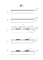
- Drawing 1 is a sectional view for explaining an example of a manufacturing method of a layered product which gave an electroless plating pattern concerning this embodiment.
- a surface treatment agent containing a polymer compound containing at least one structural unit represented by the formula (4) is applied to the surface of the substrate 11, and the photosensitive polymer layer 12 is applied. Is deposited.
- the substrate 11 may be any of general substrate materials such as an organic material, an inorganic material, and a mixed material of an inorganic material and an organic material.
- the materials used for the substrate 11 include polyethylene terephthalate (PET), polybutylene naphthalate (PBT), polyesters such as wholly aromatic polyesters; polyethylene (PE), polypropylene (PP), polystyrene, cycloolefin Polyolefins such as polymer (COP) and EVA; vinyl resins such as polyvinyl chloride and polyvinylidene chloride, and others, polyether ether ketone (PEEK), polysulfone (PSF), polyether sulfone (PES), polycarbonate (PC ), Organic materials typified by flexible plastic substrates such as polyamide, polyimide, acrylic resin, triacetyl cellulose (TAC), and typified by glass, ceramics, silicon nitride, quartz, silicon wafer, metal, etc. That is an inorganic
- any of general film formation techniques such as physical vapor deposition (PVD), chemical vapor deposition (CVD), and liquid phase growth may be used.
- the liquid phase growth method is particularly preferable.
- the liquid phase growth method include a coating method (spin coating, dip coating, die coating, spray coating, roll coating, brush coating), and a printing method (flexographic printing, screen printing). Can be mentioned. Further, a SAM film or an LB film may be used.
- a treatment for drying the solvent by heat or reduced pressure may be added.
- a photomask 13 having an exposure region of a predetermined pattern is formed.
- the exposure method is not limited to means using a photomask, and means such as projection exposure using an optical system such as a lens or a mirror, maskless exposure using a spatial light modulation element, a laser beam, or the like can be used.
- FIG. 2 is an explanatory diagram of a photoreaction mechanism when the photosensitive polymer layer 12 is exposed.
- the polymer compound contained in the photosensitive polymer layer 12 induces deprotection of the photosensitive leaving group along with decarboxylation, exposing the amino group.
- the photosensitive leaving group is maintained as it is, and the amine generation layer 14 is not formed.
- Such a mechanism makes it possible to form the position-selective amine generation layer 14.
- UV light can irradiate the wavelength with which optimal quantum efficiency is exhibited by the structure of the photosensitive group.
- i-line of 365 nm can be mentioned.
- the exposure amount and the exposure time do not necessarily require complete deprotection, and may be such that some amine is generated. At that time, in the plating process described later, conditions (such as the activity of the plating bath) according to the progress of deprotection can be appropriately changed.
- the catalyst layer 15 is formed only on the amine generation layer 14.
- any method such as a catalyst-accelerator method or an activation method may be used.
- any catalyst material may be used as long as it can carry an amine.
- the substrate 11 is immersed in an electroless plating bath to reduce metal ions on the catalyst surface, thereby depositing a plating film 16.
- the plating film 16 can be selectively deposited only on the amine generation layer 14. If the reduction is insufficient, the metal ions on the amine may be actively reduced by dipping in a reducing agent solution such as sodium hypophosphite or sodium borohydride.
- the process of removing the resist layer is not necessary.
- the catalytic reduction ability of the amine can also eliminate the catalyst activation process that is usually required, enabling high-definition patterning while realizing significant cost reduction and time reduction.
- the plating bath in the plating treatment process is usually hot water, and it is known that if a silane coupling agent is not used, it elutes into the plating bath. Adhesion improves adhesion and solubility, and it is possible to perform patterning without dissolving the film in the plating bath.
- the film can be formed with heat at about the volatilization temperature of the solvent (about 60 ° C. in the case of chloroform), patterning in a low temperature process is possible, and the PET substrate or the like is not damaged. Further, since the dip coating method can be used, it can be used very well in the R2R process.
- the polymer compound according to the present embodiment has a non-reactive molecular structure having water resistance, acid resistance, and alkali resistance required in the plating process, it is compared with a conventional silane coupling agent or the like. High stability and chemical stability. Therefore, the surface treatment agent used at the time of film formation is stable for a long period of time, and does not cause problems such as concentration change due to poor solubility, insolubilization, sedimentation, etc. during transportation, storage, and processing. Therefore, it can be used in the coating process as it is without preparations such as filtration and concentration adjustment.
- the polymer compound represented by the formula (4) according to the present embodiment is not limited to the formation of a plating pattern, but can also be used for manufacturing other devices such as a conductive material, a polymer film, and a transistor. is there. Note that the structure of the transistor is not particularly limited and can be appropriately selected depending on the purpose.
- FIG. 7 shows an example of a transistor manufactured using the polymer compound according to this embodiment.
- 7A is a top contact / bottom gate type
- FIG. 7B is a bottom contact / bottom gate type
- FIG. 7C is a top contact / top gate type
- FIG. 7D is a bottom contact / top gate type.
- the layer 21 is a base material
- the layer 22 is a gate insulating layer
- the layer 23 is a semiconductor layer
- the layer 24 is a source electrode
- the layer 25 is a drain electrode
- the layer 26 is a gate electrode
- the layer 12 is in this embodiment.
- This is a photosensitive polymer layer 12 using the polymer compound represented by the formula (4).
- the photosensitive polymer layer 12 As shown in the figure, by forming the photosensitive polymer layer 12 using the polymer compound according to the present embodiment for forming each electrode of the transistor and the metal wiring, the position selective high-definition and excellent conductivity. It is possible to
- Example 1 Synthesis of photosensitive amine-generating monomer
- the obtained precipitate was purified by a reprecipitation method using 12 ml of chloroform (Wako Pure Chemical Industries, product number: 038-02606) as a good solvent and 120 ml of 10-fold amount of methanol as a poor solvent.
- a polymer compound represented by the following formula (8) was obtained as a pale yellow solid 3.27 g (yield 82%).
- Mn number average molecular weight
- Example 3 Synthesis of allyl ester-terminated photosensitive polymer
- an allyl ester-terminated poly-2-((((4,5-dimethoxy-2-nitrobenzyl) oxy) carbonyl) amino) ethyl methacrylate (P-NBC-) represented by the following formula (9) AEMA-Allyl) was synthesized.
- trimethoxysilylethylamide-terminated photosensitive polymer By the method described below, trimethoxysilylethylamide-terminated poly-2-((((((4,5-dimethoxy-2-nitrobenzyl) oxy) carbonyl) amino) ethyl methacrylate (P -NBC-AEMA-TEOS) was synthesized.
- the polymer compound represented by the following formula (10) was obtained as 0.59 g (yield 37%) of a pale yellow solid. When these were analyzed, the number average molecular weight (Mn) was 3767.7, and it was confirmed that a 10-mer was obtained.
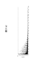
- a measurement result chart in MALDI-TOF-MS is shown in FIG.
- Example 5 Chloroform was added to P-NBC-AEMA synthesized in Example 2 to adjust to 0.2 wt%. This solution was applied on a PET substrate (Toyobo Co., Ltd., A-4100, uncoated) by spin coating (Mikasa Co., Ltd., MS-A150) 3000 rpm). Then, it was dried at 105 ° C. for 10 minutes to form a photosensitive polymer layer.
- a pattern of the generation layer was formed.
- it was immersed in a catalyst colloid solution for electroless plating (Melplate Activator 7331, manufactured by Meltex) for 3 minutes at room temperature, and the catalyst (Pd) was adhered to the amine generation part.
- Example 6 The P-NBC-AEMA of Example 5 was changed to P-NBC-AEMA-Allyl synthesized in Example 3, and the same treatment was performed to produce a fine plated wiring.
- Example 7 A fine plating wiring was produced by changing the P-NBC-AEMA of Example 5 to P-NBC-AEMA-TEOS synthesized in Example 3 and performing the same treatment.
- FIG. 5A shows a whole photograph of the PET substrate subjected to the plating wiring process in Example 5 and an optical microscope (manufactured by Keyence Corporation, VHX-900).
- FIG. 5 (b) shows a similar process performed in Example 6
- FIG. 5 (c) shows a process performed in Example 7.
- FIG. 6A shows a whole photograph of a PET substrate subjected to the plating wiring process in Comparative Example 2, and an optical microscope (manufactured by Keyence Corporation, VHX-900).
- FIG. 6B shows a similar product processed in Comparative Example 3.
- Comparative Example 3 Although the selective plating wiring was formed, it was visually confirmed that the compound was hardly soluble in the solvent over time in the chloroform solution and finally insolubilized. This is considered that the condensation reaction proceeded after hydrolysis, and the polymerization between alkoxysilanes proceeded.
- the surface treatment agent of this example sufficient adhesion can be obtained without using an adhesion mechanism using condensation between a substrate or molecules such as an alkoxysilyl group in a silane coupling agent. Obtained.
- the alkoxysilyl group does not exist or almost does not exist, after the molecular weight is increased to the desired molecular weight, the molecular weight is not further increased, and the predetermined molecular weight can be maintained in a solid or solution state. It has long-term stability, prolongs the working life, enables highly reproducible film formation, and improves the environmental resistance of the film itself. This can be expected to simplify the management and reduce the cost in the manufacturing and transportation of the film for forming a wiring, and the manufacturing process of the electronic material using the film.
- high-definition electroless plating wiring can be applied to a smooth substrate without using a resist even in a low-temperature process.
- ground treatment using many chemicals, resist development, resist stripping process, and heating process in each process including PEB that requires energy can be omitted. Can be expected.
- the organic thin film provided by the present invention functions even with an extremely thin film of about 2 to 10 nm, and the environmental load is extremely small.
Landscapes
- Chemical & Material Sciences (AREA)
- Engineering & Computer Science (AREA)
- Organic Chemistry (AREA)
- Chemical Kinetics & Catalysis (AREA)
- Materials Engineering (AREA)
- Mechanical Engineering (AREA)
- Metallurgy (AREA)
- General Chemical & Material Sciences (AREA)
- Health & Medical Sciences (AREA)
- Medicinal Chemistry (AREA)
- Polymers & Plastics (AREA)
- Manufacturing & Machinery (AREA)
- Microelectronics & Electronic Packaging (AREA)
- Life Sciences & Earth Sciences (AREA)
- Wood Science & Technology (AREA)
- Toxicology (AREA)
- Inorganic Chemistry (AREA)
- Addition Polymer Or Copolymer, Post-Treatments, Or Chemical Modifications (AREA)
- Laminated Bodies (AREA)
- Manufacturing Of Printed Wiring (AREA)
- Chemically Coating (AREA)
- Organic Low-Molecular-Weight Compounds And Preparation Thereof (AREA)
Abstract
優れた安定性と基板に対する密着性を有し、無電解めっき配線を施すことが可能な化合物を提供する。 下記式(1)で表される構成単位を有する高分子化合物。 〔式(1)中、R1は水素またはメチル基を表し、mは2~20の整数を表し、Qは感光性脱離基を表す。〕
Description
本発明は、無電解めっき形成のために用いられる化合物に関するものである。本発明は2015年4月10日に出願された日本国特許の出願番号2015-81164の優先権を主張し、文献の参照による織り込みが認められる指定国については、その出願に記載された内容は参照により本出願に織り込まれる。
無電解めっきによる微細配線を形成する方法として、例えば、特許文献1には、樹脂基体表面にエキシマ光を所望のパターンに照射し、しかる後に、アミノ基を有するシランカップリング剤、または、アミノ変性された反応性のシリコンオイルに樹脂基体を接触させ、エキシマ光の照射部に、無電解めっき反応を開始するための触媒を捕捉・固定化するための受容層を形成し、受容層上にニッケル・リンメッキ層を無電解めっきにより形成する方法が記載されている。
しかしながら、無電解めっき用の触媒を捕捉する材料として用いられている従来のシランカップリング剤は、分子内に含まれるアルコキシシリル基、もしくはハロゲン化シリル基の高い反応性により大気中の水分や溶媒に含まれる水分により加水分解を受けて縮合反応が進行し、シロキサンが生じるなど経時安定性が低いことで知られる。このような反応の結果、凝集、懸濁、沈降が進行して成膜性が低下する傾向にある。
本発明はこのような事情に鑑みてなされたものであり、優れた安定性と基板に対する密着性を有し、無電解めっき配線を施すことが可能な化合物を提供することを課題とする。
本発明者らは、優れた安定性と基板に対する密着性を有する材料として利用可能な化合物を探索した。その結果、本発明者らは、シランカップリング剤の代替物となり得る化合物群を見出し、本発明を完成するに到った。
本願は、上記課題の少なくとも一部を解決する手段を複数含んでいるが、その例を挙げるならば、以下のとおりである。
上記の課題を解決するための本発明の第一の態様は、下記式(1)で表される構成単位を有する高分子化合物。
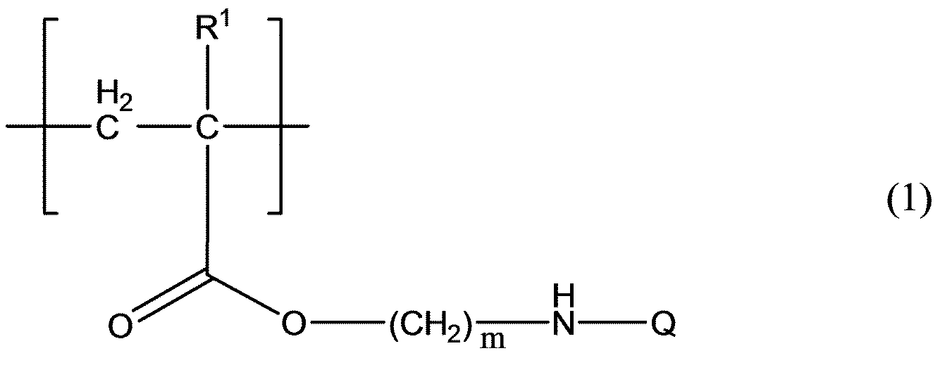
本発明の第二の態様は、Qは、少なくとも一種の下記式(2)で表される基であることを特徴とする高分子化合物。

本発明の第三の態様は、積層体の製造方法であって、上記高分子化合物を含む表面処理剤を塗布して感光性ポリマー層を形成する工程と、前記感光性ポリマー層を所定のパターン光で露光する工程と、前記感光性ポリマー層の前記露光された領域に無電解めっき用触媒を付与する工程と、前記感光性ポリマー層を無電解めっき液に接触させて無電解めっきを行う工程と、を有する積層体の製造方法である。
以下、本発明について詳細に説明する。なお、この実施の形態により本発明が限定されるものではない。また、本明細書において(メタ)アクリレートとは、アクリレートおよび/またはメタクリレートを意味する。
<高分子化合物>
本実施の形態に係る高分子化合物は、少なくとも一種の下記式(1)で表される構成単位を含む。
本実施の形態に係る高分子化合物は、少なくとも一種の下記式(1)で表される構成単位を含む。
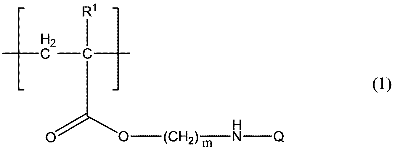
式(1)中、R1は、水素またはメチル基を表し、mは2~20の整数を表す。中でも、2~16までの整数を表されるものが好ましく、さらには、2~8までの整数で表されるものが特に好ましい。
式(1)中、Qは感光性脱離基を表す。該感光性脱離基は、構成単位中に存在するアミン保護基であり、光に反応してアミンを発生し、かつそのものは金属を捕捉しない特性があればその構造は問わない。具体的には、例えば、o-ニトロベンジル基、α-メチル-ニトロピペロニル基、α-メチル-ニトロピペロニルオキシカルボニル基、1-ピレニルメチルオキシカルボニル基、α,α-ジメチル-3,5-ジメトキシベンジルオキシカルボニル基、4-ニトロピリジンN-オキシド基、m-ニトロフェニルカルバメ-ト基、3,5-ジメトキシベンジルカルバメ-ト基、o-ニトロベンジルオキシカルボニル基、3,4-ジメトキシ-6-ニトロベンジルカルバメ-ト基、フェニル(o-ニトロフェニル)メチルカルバメ-ト基、p-メトキシフェナシル基、1,3-ジチオレン基、1,3-オキサチオレン基、p-メトキシベンジル基、トシル基、ベンゼンスルフォナミド基などを挙げることができる。
またQは、少なくとも一種の下記式(2)で表される基である。

式(2)中、R2は水素または炭素数1~10の直鎖状又は分岐鎖状、環状のアルキル基を表す。炭素数1~10のアルキル基としては、具体的には、メチル基、エチル基、n-プロピル基、イソプロピル基、n-ブチル基、t-ブチル基、シクロヘキシル基等が挙げられる。この中でも好ましくはイソプロピル基、エチル基、メチル基であり、特に好ましくはイソプロピル基、メチル基である。
R3及びR4はそれぞれ独立して炭素数1~30の直鎖状又は分岐鎖状のアルキル基または炭素数1~30の直鎖状又は分岐鎖状のフルオロアルキル基を表す。炭素数1~30のアルキル基としては、具体的には、メチル基、エチル基、n-プロピル基、イソプロピル基、n-ブチル基、t-ブチル基、デシル基等が挙げられ、この中でも直鎖状のアルキル基が好ましく、特に好ましくはメチル基である。
炭素数1~30のフルオロアルキル基としては、具体的には、トリフルオロメチル基、ペンタフルオロエチル基、ヘプタフルオロプロピル基、1-(トリフルオロメチル)-1,2,2,2-テトラフルオロエチル基、ノナフルオロブチル基、1,1-ジ(トリフルオロメチル)-2,2,2-トリフルオロエチル基、ウンデカフルオロペンチル基、トリデカフルオロヘキシル基、ペンタデカフルオロヘプチル基、ヘプタデカフルオロオクチル基、ヘプタデカフルオロウンデシル基、トリデカフルオロノニル基、トリフルオロデシル基などが挙げられ、この中でも好ましくはヘプタデカフルオロウンデシル基、トリデカフルオロノニル基であり、特に好ましくはヘプタデカフルオロウンデシル基である。
なお、R3及びR4は、それぞれ独立に選択することができ、同じ置換基であってもよいし、異なる置換基であってもよい。
R5は水素またはニトロ基を表す。
Qが式(2)で表される基である式(1)で表される高分子化合物は、例えば、下記式(3)で表される化合物(モノマー)を重合することで得られ、下記式(4)のように表される。


式(3)及び(4)において、R1~R5、mは、前記と同じ意味を表す。
式(3)で表される化合物の重合は特に限定されないが、制御の容易性等の観点からラジカル重合法が好ましく、ラジカル重合の中でも、制御ラジカル重合がより好ましい。制御ラジカル重合法としては、連鎖移動剤法、リビング重合の一種であるリビングラジカル重合法等が挙げられるが、分子量分布の制御が容易であるリビングラジカル重合がさらに好ましい。なお、リビングラジカル重合法としては、ニトロキシラジカル重合法(NMP)、原子移動ラジカル重合法(ATRP)、可逆的付加解裂連鎖移動法(RAFT)等があるが、温度や汎用性の観点から、特に原子移動ラジカル重合法(ATRP)が望ましい。
なお、ラジカル重合を用いる場合には、従来公知の重合開始剤を適宜用いることができる。また、ラジカル重合開始剤は、単独又は二種以上を使用してもよく、また、市販されているものをそのまま使用してもよい。
例えば、アゾ基(-N=N-)を有し、N2とラジカルを発生する化合物であるアゾ重合開始剤を用いることができる。具体的には、アゾニトリル、アゾエステル、アゾアミド、アゾアミジン、アゾイミダゾリン等が挙げられる。さらに具体的には、例えば、2,2’-アゾビス(2-アミジノプロパン)ジハイドロクロライド、4,4’-アゾビス(4-シアノヴァレリックアシド)、2,2’-ビス(2-イミダゾリン-2-イル)-2,2’-アゾプロパンジハイドロクロライド、2,2’-ビス(2-イミダゾリン-2-イル)-2,2’-アゾプロパン、2,2’-アゾビス[N-(2-ヒドロキシエチル)-2-メチルプロピオンアミド]、2,2’-アゾビスイソブチロニトリル(AIBN)、2,2’-アゾビス(2,4-ヂメチルバレロニトリル)(ADBN)が挙げられる。この中でも好ましくは2,2’-アゾビスイソブチロニトリル(AIBN)、2,2’-アゾビス(2,4-ヂメチルバレロニトリル)(ADBN)であり、特に好ましくは2,2’-アゾビスイソブチロニトリル(AIBN)である。
特にリビングラジカル重合に用いる場合の重合開始剤としては、例えば、原子移動ラジカル重合法(ATRP)の重合開始剤として従来公知のものを適宜用いることができる。具体的には、例えば、1-フェニルエチルクロリド、1-フェニルエチルブロミド、クロロホルム、四塩化炭素、2-ブロモプロピオニトリル、2-クロロプロピオン酸およびその誘導体、2-ブロモプロピオン酸およびその誘導体、2-クロロイソ酪酸およびその誘導体、2-ブロモイソ酪酸およびその誘導体などの有機ハロゲン化合物が挙げられる。この中でも好ましくは2-ブロモプロピオン酸およびその誘導体であり、特に好ましくは2-ブロモ-2-メチルプロピオン酸アリル、N-[3-(トリメトキシシリル)プロピル]-2-ブロモ-2-メチルプロピオンアミドである。
なお、その他の添加剤についても、適宜用いることができる。例えば、重合反応に用いる触媒を、重合法に応じて従来公知のものを適宜用いることができる。例えば、原子移動ラジカル重合法(ATRP)に用いる触媒としては、例えば、Cu、Fe、Ru等の金属を含有する金属触媒を用いることができる。特に0価の銅、及びCu+を含む1価の銅化合物が好ましい。具体的には、例えば、Cu(0)、CuCl、CuBr、Cu2O等が挙げられる。安定性に優れる2価の金属触媒を用い、例えばAIBNやアスコルビン酸などを用いて反応液中で1価に還元させても良い。
また、金属触媒に応じた配位子を適宜用いることもできる。配位子としては、例えば、2,2’-ビピリジンおよびその誘導体、1,10-フェナントロリンおよびその誘導体、テトラメチルエチレンジアミン、ペンタメチルジエチレントリアミン、トリス(ジメチルアミノエチル)アミン(Me6TREN)、トリフェニルホスフィン、トリブチルホスフィン等が挙げられる。
さらに、密着性、塗布均一性、耐薬品性、耐熱性等の特性を付与するために、他の一般的な添加剤を加えることもできる。
このようにして合成される式(4)で表される構成単位を有する高分子化合物の数平均分子量は、めっき浴などへの溶解・剥離のリスクを下げ、溶解性を担保するという観点からは、湿式成膜できる程度の500以上10000以下であるのが好ましく、より好ましくは800以上6000以下であり、さらに好ましくは1000以上5000以下である。また同様の理由から、分子量分布のピークは、1000~6000の範囲であるのが好ましく、より好ましくは1000~5000の範囲である。これらは、ゲルパーミエーションクロマトグラフィー(GPC)によって測定可能である。
なお、少なくとも一種の式(4)で示される構成単位を含む(メタ)アクリレート化合物を、二種以上含む混合物であってもよい。また、式(4)で示される以外の他の任意の構成単位を一種または二種以上含むコポリマ-でもよい。
式(3)で表される化合物(モノマー)は、例えば、下記式(5)で表される化合物と、下記式(6)で表される化合物とをウレタン化反応させることによって得られる。

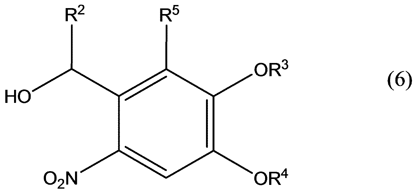
式(5)及び(6)において、R1~R5、mは、前記と同じ意味を表す。
上記式(5)で表される化合物は、例えば、メタクリル酸2-イソシアナトエチル、メタクリル酸3-イソシアナトプロピル、メタクリル酸4-イソシアナトブチル、メタクリル酸5-イソシアナトペンチル等が挙げられる。中でも、メタクリル酸2-イソシアナトエチルが好ましい。
上記式(6)で表される化合物は、例えば、4,5-ジメトキシ-2-ニトロベンジルアルコール、4,5-ジエトキシ-2-ニトロベンジルアルコール、4,5-ジプロポキシ-2-ニトロベンジルアルコール、3,4-ジメトキシ-2,6-ジニトロベンジルアルコール、3,4-ジエトキシ-2,6-ジニトロベンジルアルコール、3,4-ジプロポキシ-2,6-ジニトロベンジルアルコール、1-(4,5-ジメトキシ-2-ニトロフェニル)エタノール、1-(4,5-ジエトキシ-2-ニトロフェニル)エタノール、1-(4,5-ジプロポキシ-2-ニトロフェニル)エタノール1-(4,5-ジメトキシ-2-ニトロフェニル)プロパノール、1-(4,5-ジエトキシ-2-ニトロフェニル)プロパノール、1-(4、5-ジプロポキシ-2-ニトロフェニル)プロパノール、1-(4,5-ジメトキシ-2-ニトロフェニル)ブタノール、1-(4,5-ジエトキシ-2-ニトロフェニル)ブタノール、1-(4,5-ジプロポキシ-2-ニトロフェニル)ブタノール、1-(3,4-ジメトキシ-2,6-ジニトロフェニル)エタノール、1-(3,4-ジエトキシ-2,6-ジニトロフェニル)エタノール、1-(3,4-ジプロポキシ-2,6-ジニトロフェニル)エタノール、1-(3,4-ジメトキシ-2,6-ジニトロフェニル)プロパノール、1-(3,4-ジエトキシ-2,6-ジニトロフェニル)プロパノール、1-(3,4-ジプロポキシ-2,6-ジニトロフェニル)プロパノール、1-(3,4-ジメトキシ-2,6-ジニトロフェニル)ブタノール、1-(3,4-ジエトキシ-2,6-ジニトロフェニル)ブタノール、1-(3,4-ジプロポキシ-2,6-ジニトロフェニル)ブタノール、等が挙げられる。中でも、4,5-ジメトキシ-2-ニトロベンジルアルコールが好ましい。
本反応において、式(5)で表される化合物に対する式(6)で表される化合物の量は、モル比で0.2~5倍量であり、より好ましくは0.5~1倍量である。
式(5)で表される化合物と、式(6)で表される化合物とをウレタン化反応させる際には、反応時間の短縮等の観点から、ウレタン化反応触媒を用いてもよい。
ウレタン化反応触媒としては、例えば、N-メチルモルフォリン、N-エチルモルフォリン、ジモルフォリノメタン、エチルモルフォリノ酢酸、N-(3-ジメチルアミノプロピル)モルフォリン、N-メチルピペリジン、キノリン、1,2-ジメチルイミダゾール、N-メチルジシクロヘキシルアミン、トリエチルアミン、ピリジン、1,4-ジアザビシクロオクタン、テトラメチル-1,3-ブタンジアミン、テトラメチル-1,3-プロパンジアミン、ジメチルジエチル-1,3-プロパンジアミン、ペンタメチルジエチレンジアミン、テトラエチルメタンジアミン、ビス(2-ジメチルアミノエチル)アジペート、ビス(2-ジエチルアミノエチル)アジペート、ジメチルシクロヘキシルアミン、ジエチルシクロヘキシルアミン、メチルオクチルシクロヘキシルアミン、メチルドデシルシクロヘキシルアミン等の3級アミン化合物;塩化スズ、テトラ-N-ブチルスズ、テトラフェニルスズ、トリ-n-ブチルスズアセテート、ジメチルジクロロスズ、ジ-n-ブチルスズジアセテート、ジ-n-ブチルジクロロスズ、ジ-n-ブチルスズジラウレート(DBTDL)、ジ-n-ブチルスズジジラウリン酸メルカプチド、ビス(2-エチルヘキシル)スズオキシド、ジ-n-ブチルスズスルフィド等の含スズ化合物が挙げられる。中でも、ジ-n-ブチルスズジラウレート(DBTDL)が好ましい。
ウレタン化反応触媒の使用量は、式(5)で表される化合物100質量部に対して、0.01~1質量部であり、より好ましくは0.01~0.1質量部である。
本反応は、無溶媒でも進行させることが可能であるが、溶媒の存在可で行うことも可能である。溶媒は、化合物に対して反応性を有さない溶媒が望ましく、例えば、アセトン、テトラヒドロフラン、アセトニトリル、クロロホルム、ジクロロメタン、ベンゼン、トルエン、ヘキサン、ピリジン等が挙げられる。中でも、テトラヒドロフランが好ましい。
本反応の反応温度は、上記溶媒の温度等によって適宜調節することが可能であるが、反応時間と副反応の抑制の観点からは、0~100℃、好ましくは30~80℃の範囲であることが望ましい。
このようなウレタン化反応により、式(3)で表されるウレタン結合を含有する(メタ)アクリレート化合物の前駆体を得ることができる。得られた化合物(3)から、上記重合法によって式(4)で表される(メタ)アクリレート化合物を得ることができる。このような高分子化合物は、例えば、以下のようにして調整することができる。
<表面処理剤>
少なくとも一種の式(4)で示される構成単位を含む高分子化合物は、例えば、一般的な有機溶媒に溶かすことで、無電解めっきにおいて好適な表面処理剤として用いることができる。有機溶媒は揮発温度や公害性等の条件に応じて適宜選択することができ、例えば、メタノール、エタノール、プロパノール、イソプロパノール、ブタノール、クロロベンゼン、ジクロロメタン、クロロホルム、テトラクロロエタン、アセトニトリル、ベンゼン、トルエン、o-ジクロロベンゼン、テトラヒドロフラン、メチルイソブチルケトン、1,4-ジオキサン、シクロヘキサノン、メチルイソブチルケトン、メチルエチルケトン、ジメチルホルムアミド、ジメチルアセトアミド、アセトン、ヘキサン、酢酸エチル等が挙げられる。これらは、1種単独で使用してもよく、2種以上を併用してもよい。
少なくとも一種の式(4)で示される構成単位を含む高分子化合物は、例えば、一般的な有機溶媒に溶かすことで、無電解めっきにおいて好適な表面処理剤として用いることができる。有機溶媒は揮発温度や公害性等の条件に応じて適宜選択することができ、例えば、メタノール、エタノール、プロパノール、イソプロパノール、ブタノール、クロロベンゼン、ジクロロメタン、クロロホルム、テトラクロロエタン、アセトニトリル、ベンゼン、トルエン、o-ジクロロベンゼン、テトラヒドロフラン、メチルイソブチルケトン、1,4-ジオキサン、シクロヘキサノン、メチルイソブチルケトン、メチルエチルケトン、ジメチルホルムアミド、ジメチルアセトアミド、アセトン、ヘキサン、酢酸エチル等が挙げられる。これらは、1種単独で使用してもよく、2種以上を併用してもよい。
<無電解めっきパターン形成>
本実施形態に係る表面処理剤によれば、例えば、次のような方法によって無電解めっきパターンを形成することができる。図1は、本実施形態に係る無電解めっきパターンを施した積層体の製造方法の一例を説明するための断面図である。
本実施形態に係る表面処理剤によれば、例えば、次のような方法によって無電解めっきパターンを形成することができる。図1は、本実施形態に係る無電解めっきパターンを施した積層体の製造方法の一例を説明するための断面図である。
(第1の工程)
まず、図1(a)に示すように、基板11の表面に、少なくとも一種の式(4)で示される構成単位を含む高分子化合物を含有した表面処理剤を塗布して感光性ポリマー層12を成膜する。
まず、図1(a)に示すように、基板11の表面に、少なくとも一種の式(4)で示される構成単位を含む高分子化合物を含有した表面処理剤を塗布して感光性ポリマー層12を成膜する。
なお、基板11は有機材料や無機材料、及び無機系材料と有機系材料の混合材料等、一般的な基板材料のいずれのものであっても良い。具体的に、基板11に用いられる材料としては、ポリエチレンテレフタレート(PET)、ポリブチレンナフタレート(PBT)、全芳香族ポリエステルなどのポリエステル類;ポリエチレン(PE)、ポリプロピレン(PP)、ポリスチレン、シクロオレフィンポリマー(COP)、EVAなどのポリオレフィン類;ポリ塩化ビニル、ポリ塩化ビニリデンなどのビニル系樹脂、その他、ポリエーテルエーテルケトン(PEEK)、ポリサルホン(PSF)、ポリエーテルサルホン(PES)、ポリカーボネート(PC)、ポリアミド、ポリイミド、アクリル樹脂、トリアセチルセルロース(TAC)などの可撓性プラスチック基板に代表される有機材料、及び、ガラス、セラミックス、窒化ケイ素、石英、シリコンウエハ、金属等に代表される無機材料である。さらに、離型フィルム上に形成した熱硬化系樹脂あるいは光硬化系樹脂等の架橋構造を有する基板でもかまわない。
塗布方法としては、物理的気相成長法(PVD)や化学的気相成長法(CVD)、液相成長法等、一般的な成膜技術の何れを用いてもよい。中でも、特に液相成長法が好ましく、液相成長法としては例えば、塗布法(スピンコート、ディップコート、ダイコート、スプレーコート、ロールコート、刷毛塗り)、印刷法(フレキソ印刷、スクリーン印刷)等が挙げられる。また、SAM膜、LB膜としてもよい。
なお、本工程においては、例えば熱や減圧等によって溶剤を乾燥させる処理を加えてもよい。
(第2の工程)
次に、図1(b)に示すように、所定のパターンの露光領域を有するフォトマスク13を形成する。露光方法としては、フォトマスクを用いる手段に限られず、レンズやミラーなどの光学系を用いたプロジェクション露光、空間光変調素子、レーザービームなどを用いたマスクレス露光等の手段を用いることができる。
次に、図1(b)に示すように、所定のパターンの露光領域を有するフォトマスク13を形成する。露光方法としては、フォトマスクを用いる手段に限られず、レンズやミラーなどの光学系を用いたプロジェクション露光、空間光変調素子、レーザービームなどを用いたマスクレス露光等の手段を用いることができる。
(第3の工程)
その後、図1(c)に示すように、全体にUV光を照射する。これにより、フォトマスク13の露光領域において感光性ポリマー層12が露光し、アミン発生層14が形成される。
その後、図1(c)に示すように、全体にUV光を照射する。これにより、フォトマスク13の露光領域において感光性ポリマー層12が露光し、アミン発生層14が形成される。
図2は、感光性ポリマー層12が露光した際の光反応機構についての説明図である。UV光に曝されると、感光性ポリマー層12に含まれる高分子化合物は、脱炭酸に伴って感光性脱離基の脱保護が誘発され、アミノ基を露出する。一方、マスクされた非露光領域においては脱保護が進行しないため、感光性脱離基はそのまま維持されアミン発生層14は形成されない。このような機構により、位置選択的なアミン発生層14の形成が可能となる。
なお、UV光は感光性基の構造により最適な量子効率が発揮される波長を照射することができる。例えば、365nmのi線が挙げられる。また、その露光量や露光時間は、必ずしも完全に脱保護が進行する必要はなく、一部のアミンが発生する程度でよい。その際、後述のめっき工程において、脱保護の進行具合に応じた条件(めっき浴の活性等)を適宜変更することができる。
(第4の工程)
次に、図1(d)に示すように、表面に触媒を付与する。
次に、図1(d)に示すように、表面に触媒を付与する。
具体的に本工程では、1級アミンを含むアミン発生層14のみが触媒物質を捕捉・還元することが可能であるため、アミン発生層14上のみに触媒層15が形成される。なお、触媒化の方法としては、キャタリスト-アクセラレータ法、アクティベーティング法等、どのような方法を用いてもよい。また、触媒物質もアミンが担持可能なものであれば、どのようなものを用いても構わない。
(第5の工程)
最後に、図1(e)に示すように、無電解めっき処理を行い、めっき膜16を形成する。
最後に、図1(e)に示すように、無電解めっき処理を行い、めっき膜16を形成する。
具体的に本工程では、基板11を無電解めっき浴に浸漬して触媒表面に金属イオンを還元し、めっき膜16を析出させる。その際、アミン発生層14表面には十分な量の触媒を担持する触媒層15が形成されているため、アミン発生層14上にのみ選択的にめっき膜16を析出させることができる。還元が不十分な場合には、次亜リン酸ナトリウム、水素化ホウ素ナトリウムなどの還元剤溶液に浸漬してアミン上の金属イオンを積極的に還元してもよい。
上記のような方法によれば、UV露光工程において別途化学的なレジスト等を設ける必要がなく、フォトマスクのみによる簡素な工程とすることができる。従って当然ながら、レジスト層を除去する工程についても必要しない。また、アミンの触媒還元能により、通常必要となる触媒の活性化処理工程も省略することができ、大幅な低コスト化と時間短縮を実現しながら、高精細なパターニングが可能となる
また、めっき処理工程におけるめっき浴は通常熱水であり、シランカップリング剤を用いない場合にはめっき浴に溶出することが知られているが、本実施形態に係る高分子化合物では、高分子量化によって密着性が向上すると共に溶解性が制御され、膜をめっき浴に溶解させることなく、パターニングを行うことが可能となる。
さらに、溶媒の揮発温度程度(クロロホルムであれば約60℃)の熱で成膜を行えるため、低温プロセスでのパターニングが可能であり、PET基板等にもダメージを与えることがない。また、ディップコート法を用いることができるため、R2R工程でも非常に相性良く利用することができる。
加えて、本実施形態に係る高分子化合物は、めっき工程で求められる耐水性、耐酸性、耐アルカリ性を有する非反応性の分子構造をもつため、従来のシランカップリング剤等と比較して大気安定性や化学安定性が高い。よって、成膜時に用いる表面処理剤は長期に亘り安定であり、運搬・保存・処理時において難溶化・不溶化・沈降等による濃度変化等の問題を生じることがない。よって、濾過や濃度調整等の前準備を行わずに、そのまま塗布工程に利用することができる。
また、めっき工程で用いられる酸性溶液や熱水、その他例えばアルカリ性溶液等に曝された場合でも分解・剥離が生じることなく、ポリマーによる基板への強固な密着性が保たれる。さらには、アルコキシシランを持たない難水溶性光アミン発生剤を低分子量のまま用いた場合と比較しても、耐めっき性が高くめっき工程での溶解・剥離が生じない。
また、本実施形態に係る式(4)で表される高分子化合物は、めっきパターンの形成に限らず、導電性材料、高分子フィルム、トランジスタ等、他のデバイスの製造に用いることも可能である。なお、トランジスタの構造としては、特に制限はなく、目的に応じて適宜選択することができる。
図7に、本実施形態に係る高分子化合物を用いて製造したトランジスタの例を示す。図7(a)はトップコンタクト・ボトムゲート型、図7(b)はボトムコンタクト・ボトムゲート型、図7(c)はトップコンタクト・トップゲート型、図7(d)はボトムコンタクト・トップゲート型の例である。図中、層21は基材、層22はゲート絶縁層、層23は半導体層、層24はソース電極、層25はドレイン電極、層26はゲート電極を示し、層12は、本実施形態に係る式(4)で表される高分子化合物を用いた感光性ポリマー層12である。図示するように、トランジスタの各電極、及び金属配線の形成に本実施形態に係る高分子化合物を用いた感光性ポリマー層12を成膜することで、位置選択的に高精細かつ導電性に優れた電極及び微細配線を形成することが可能である。
以下に、実施例および比較例を示し、本発明をより具体的に説明する。ただし、本発明は、これらの実施例によって限定されるものではない。
[実施例1:感光性アミン発生モノマーの合成]
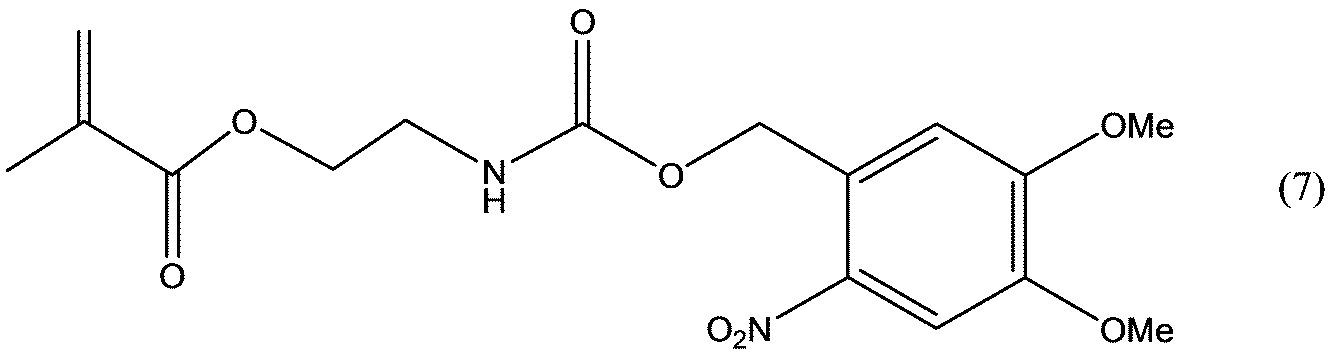
下記に記載する方法により、下記式(7)で表される2-((((4,5-ジメトキシ-2-ニトロベンジル)オキシ)カルボニル)アミノ)エチルメタクリレート(NBC-AEMA)を合成した。
下記に記載する方法により、下記式(7)で表される2-((((4,5-ジメトキシ-2-ニトロベンジル)オキシ)カルボニル)アミノ)エチルメタクリレート(NBC-AEMA)を合成した。
セプタム、三方コックを接続した3つ口丸底フラスコに、4,5-ジメトキシ-2-ニトロベンジルアルコール(シグマアルドリッチ、製品番号:392847)を7.98g(37.47mmol)を量り入れ、窒素置換した。無水THF(シグマアルドリッチ、製品番号401757)100ml、ジブチルチンラウリレート(東京化成工業、製品番号:D0303)を0.10g(6.63mmol)、メタクリル酸2-イソシアナトエチル(東京化成工業、製品番号:I0748)を6.97g(44.96mmol)を量り入れ、10分程度撹拌した。80℃で2時間還流させた後、ロータリーエバポレーターおよび真空ポンプを用いて減圧乾燥させ粗生成物を18.974g得た。その後、ナスフラスコ中で粗生成物を酢酸エチル(和光純薬工業、製品番号:051-00351)50mlに溶解させ、ヘキサン(和光純薬工業、製品番号:085-00411)100mlを加え、貧溶媒添加法による固体析出によって精製を行った。析出した固体を10umのフィルターを用いてろ取し、真空ポンプによる減圧乾燥を行うことで、下記式(7)で表される化合物を、淡黄色紛体13.33g(36.21mmol、収率97%)で得た。
1H-NMR(ブルカーバイオスピン株式会社、AVANCEIII HD 500MHz),及びESI-MS(株式会社島津製作所、LCMS2020)の測定結果を以下に示す。
1H-NMR(500MHz,CDCl3):δ1.94(3H,s),3.55(2H,d),3.95and3.97(3H,s),4.26(2H,d),5.59(1H,s),5.89(1H,br),6.11(1H,s),7.00(1H,s),7.70(1H,s)
ESI-MS:C16H21N2O8 +(M+H+)の計算値m/z=369、実測値m/z=369
1H-NMR(500MHz,CDCl3):δ1.94(3H,s),3.55(2H,d),3.95and3.97(3H,s),4.26(2H,d),5.59(1H,s),5.89(1H,br),6.11(1H,s),7.00(1H,s),7.70(1H,s)
ESI-MS:C16H21N2O8 +(M+H+)の計算値m/z=369、実測値m/z=369
[実施例2:感光性ポリマーの合成]
下記に記載する方法により、下記式(8)で表されるポリ2-((((4,5-ジメトキシ-2-ニトロベンジル)オキシ)カルボニル)アミノ)エチルメタクリレート(P-NBC-AEMA)を合成した。
下記に記載する方法により、下記式(8)で表されるポリ2-((((4,5-ジメトキシ-2-ニトロベンジル)オキシ)カルボニル)アミノ)エチルメタクリレート(P-NBC-AEMA)を合成した。
セプタム、三方コックを接続した3つ口ヘルツ型フラスコに、実施例1で合成した2-((((4,5-ジメトキシ-2-ニトロベンジル)オキシ)カルボニル)アミノ)エチルメタクリレートを4.00g(10.90mmol)、2,2’-アゾビス(イソブチロニトリル)(東京化成工業、製品番号:A0566)を178.92mg(1.09mmol)量り入れた。窒素置換後、脱気処理した無水DMF(シグマアルドリッチ、製品番号:227056)を5.5ml加え、真空ポンプを用い減圧下での超音波照射による脱気処理を行った。これを80℃で70時間加熱撹拌した後、室温まで放冷した。ガラス管にメタノール(和光純薬工業、製品番号:137-01823)120mlを入れ、撹拌子で強撹拌させながら反応液をこれに滴下した。30分間撹拌した後、析出物を沈降させ上澄みを除去した後減圧乾燥を行った。得られた析出物に対し、良溶媒としてクロロホルム(和光純薬工業、製品番号:038-02606)12ml、貧溶媒として10倍量のメタノール120mlを用いて再沈殿法による精製を行った。精製を3回繰り返すことで、下記式(8)で表される高分子化合物を、淡黄色固体3.27g(収率82%)として得た。これらを分析したところ、数平均分子量(Mn)は3893.5であり、10量体が得られていることを確認した。MALDI-TOF-MSにおける測定結果のチャートを、図3(a)に示した。
1H-NMR(ブルカーバイオスピン株式会社、AVANCEIII HD 500MHz),及びMALDI-TOF-MS(日本電子株式会社、JMS-S3000)の測定結果を以下に示す。
1H-NMR(500MHz,CDCl3):δ0.85-1.55(m),1.85(2H,m),3.45(2H,m),3.92(6H,m),4.03(2H,m),5.42(2H,m),6.09(1H,m),6.98(1H,m),7.59(1H,m),
TOF-MS:(C16H20N2O8)5+C4H6N+C16H19N2O8+Na+(M+Na+)の計算値m/z=1930.6、実測値m/z=1930.6
1H-NMR(500MHz,CDCl3):δ0.85-1.55(m),1.85(2H,m),3.45(2H,m),3.92(6H,m),4.03(2H,m),5.42(2H,m),6.09(1H,m),6.98(1H,m),7.59(1H,m),
TOF-MS:(C16H20N2O8)5+C4H6N+C16H19N2O8+Na+(M+Na+)の計算値m/z=1930.6、実測値m/z=1930.6

[実施例3:アリルエステル末端感光性ポリマーの合成]
下記に記載する方法により、下記式(9)で表されるアリルエステル末端ポリ2-((((4,5-ジメトキシ-2-ニトロベンジル)オキシ)カルボニル)アミノ)エチルメタクリレート(P-NBC-AEMA-Allyl)を合成した。
下記に記載する方法により、下記式(9)で表されるアリルエステル末端ポリ2-((((4,5-ジメトキシ-2-ニトロベンジル)オキシ)カルボニル)アミノ)エチルメタクリレート(P-NBC-AEMA-Allyl)を合成した。
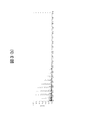
セプタム、三方コックを接続した2つ口ヘルツ型フラスコに、臭化銅(I)(シグマアルドリッチ、製品番号:254185)を58.5mg(0.41mmol)量り入れた。窒素置換後、脱気処理した無水DMF(シグマアルドリッチ、製品番号:227056)を0.5ml、トリス[2-(ジメチルアミノ)エチル]アミン(シグマアルドリッチ、製品番号:723142)を109.2ul(0.41mmol)加え、真空ポンプを用い減圧下での超音波照射による脱気処理を行い完全に溶解させた。さらに室温で30分間撹拌した後、実施例1で合成した2-((((4,5-ジメトキシ-2-ニトロベンジル)オキシ)カルボニル)アミノ)エチルメタクリレートを1.5g(4.09mmol)、脱気処理した無水DMFを1ml量り入れた。そして、無水DMF0.5mlに2-ブロモ-2-メチルプロピオン酸アリル84.6mg(0.41mmol)を溶解させ反応器内に滴下し、室温で66時間撹拌した。ガラス管にメタノール(和光純薬工業、製品番号:137-01823)80mlを入れ、撹拌子で強撹拌させながら反応液をこれに滴下した。10分間撹拌した後、析出物を沈降させ上澄みを除去した後減圧乾燥を行った。得られた析出物に対し、良溶媒としてDMF3ml、貧溶媒としてメタノール80mlを用いて再沈殿法による精製を行った。得られた析出物に対し、さらに良溶媒としてクロロホルム(和光純薬工業、製品番号:038-02606)10ml、貧溶媒として10倍量のメタノール100mlを用いて再沈殿法による精製を2回行うことで、下記式(9)で表される高分子化合物を、淡黄色固体1.04g(収率63%)として得た。これらを分析したところ、数平均分子量(Mn)は4635.5であり、10量体が得られていることを確認した。MALDI-TOF-MSにおける測定結果のチャートを、図3(b)に示した。
1H-NMR(ブルカーバイオスピン株式会社、AVANCEIII HD 500MHz),及びMALDI-TOF-MS(日本電子株式会社、JMS-S3000)の測定結果を以下に示す。
1H-NMR(500MHz,CDCl3):δ0.87-1.70(m),1.82(2H,m),3.44-3.49(m),3.92(6H,m),4.04(2H,m),5.42(2H,m),6.05(1H,m),6.98(1H,m),7.58(2H,m)
TOF-MS:(C16H20N2O8)3+ C7H11O2 + C16H19N2O8+Na+(M+Na+)の計算値m/z=1621.5、実測値m/z=1621.5
1H-NMR(500MHz,CDCl3):δ0.87-1.70(m),1.82(2H,m),3.44-3.49(m),3.92(6H,m),4.04(2H,m),5.42(2H,m),6.05(1H,m),6.98(1H,m),7.58(2H,m)
TOF-MS:(C16H20N2O8)3+ C7H11O2 + C16H19N2O8+Na+(M+Na+)の計算値m/z=1621.5、実測値m/z=1621.5

[実施例4:トリメトキシシリルエチルアミド末端感光性ポリマーの合成]
下記に記載する方法により、下記式(10)で表されるトリメトキシシリルエチルアミド末端ポリ2-((((4,5-ジメトキシ-2-ニトロベンジル)オキシ)カルボニル)アミノ)エチルメタクリレート(P-NBC-AEMA-TEOS)を合成した。
下記に記載する方法により、下記式(10)で表されるトリメトキシシリルエチルアミド末端ポリ2-((((4,5-ジメトキシ-2-ニトロベンジル)オキシ)カルボニル)アミノ)エチルメタクリレート(P-NBC-AEMA-TEOS)を合成した。
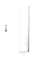
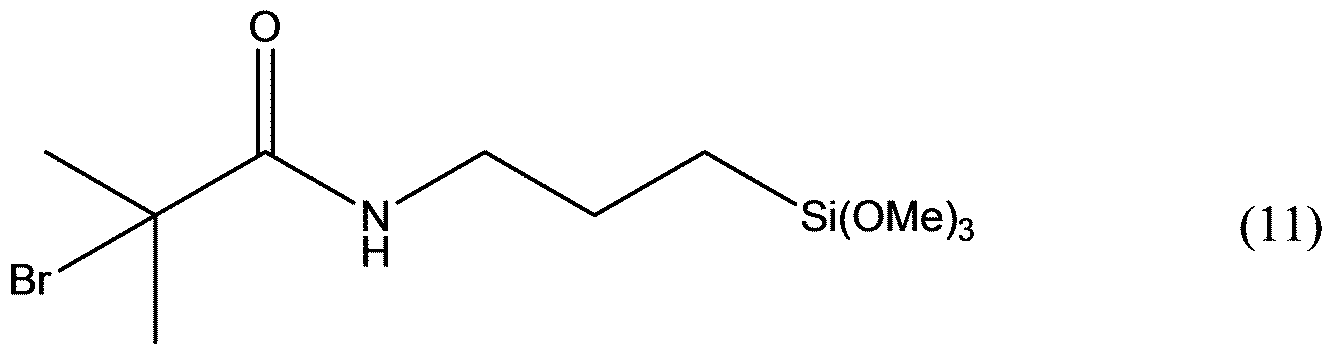
セプタム、三方コックを接続した2つ口ヘルツ型フラスコに、臭化銅(I)(シグマアルドリッチ、製品番号:254185)を58.5mg(0.41mmol)量り入れた。窒素置換後、脱気処理した無水DMF(シグマアルドリッチ、製品番号:227056)を0.5ml、トリス[2-(ジメチルアミノ)エチル]アミン(シグマアルドリッチ、製品番号:723142)を109.2ul(0.41mmol)加え、真空ポンプを用い減圧下での超音波照射による脱気処理を行い完全に溶解させた。さらに室温で30分間撹拌した後、実施例1で合成した2-((((4,5-ジメトキシ-2-ニトロベンジル)オキシ)カルボニル)アミノ)エチルメタクリレートを1.5g(4.09mmol)、脱気処理した無水DMFを1ml量り入れた。無水DMF0.5mlに、下記式(11)で表される2-ブロモ-2-メチル-N-(3-(トリメトキシシリル)プロピル)プロパンアミド151.3mg(0.41mmol)を溶解させ反応器内に滴下し、室温で66時間撹拌した。ガラス管にメタノール(和光純薬工業、製品番号:137-01823)80mlを入れ、撹拌子で強撹拌させながら反応液をこれに滴下した。10分間撹拌した後、析出物を沈降させ上澄みを除去した後減圧乾燥を行った。得られた析出物に対し、良溶媒としてDMF3ml、貧溶媒としてメタノール80mlを用いて再沈殿法による精製を行った。得られた析出物に対し、良溶媒としてクロロホルム(和光純薬工業、製品番号:038-02606)10ml、貧溶媒として10倍量のメタノール100mlを用いて再沈殿法による精製を2回行うことで、下記式(10)で表される高分子化合物を、淡黄色固体0.59g(収率37%)として得た。これらを分析したところ、数平均分子量(Mn)は3767.7であり、10量体が得られていることを確認した。MALDI-TOF-MSにおける測定結果のチャートを、図3(c)に示した。
1H-NMR(ブルカーバイオスピン株式会社、AVANCEIII HD 500MHz),及びMALDI-TOF-MS(日本電子株式会社、JMS-S3000)の測定結果を以下に示す。
1H-NMR(500MHz,CDCl3):δ0.87-1.82(m),1.88(2H,m),3.45-3.49(m),3.92(6H,m),4.04(2H,m),5.42(2H,m),6.10(1H,m),6.98(1H,m),7.58(2H,m),
TOF-MS:(C16H20N2O8)3+ C10H22NO4Si + C16H19N2O8+Na+(M+Na+)の計算値m/z=1742.6、実測値m/z=1742.6
1H-NMR(500MHz,CDCl3):δ0.87-1.82(m),1.88(2H,m),3.45-3.49(m),3.92(6H,m),4.04(2H,m),5.42(2H,m),6.10(1H,m),6.98(1H,m),7.58(2H,m),
TOF-MS:(C16H20N2O8)3+ C10H22NO4Si + C16H19N2O8+Na+(M+Na+)の計算値m/z=1742.6、実測値m/z=1742.6

なお、本実施で用いた下記式(11)で表される2-ブロモ-2-メチル-N-(3-(トリメトキシシリル)プロピル)プロパンアミドは、以下のように合成した。
セプタム、三方コックを接続した3つ口丸底フラスコに、4-ジメチルアミノピリジン(東京化成工業、製品番号:D1450)を0.3g(2.7mmol)を量り入れた。窒素雰囲気下で無水THF(シグマアルドリッチ、製品番号401757)100mlを量り入れ0℃に冷却した後、α-ブロモイソブチリルブロミド(シグマアルドリッチ、製品番号:252271)を6.2g(26.9mmol)、トリエチルアミン(和光純薬工業、製品番号:20-0264)を2.7g(26.9mmol)加えた。次いで滴下ロートを用い、3-アミノプロピルトリメトキシシラン(東京化成工業、製品番号:T1255)3.7g(20.7mmol)を30分間かけて滴下した。室温で23時間撹拌後、0.2umのフィルターを用いて減圧ろ過し、ろ液をロータリーエバポレーターにより減圧乾燥させた。その後酢酸エチル(和光純薬工業、製品番号:051-00351)100mlに溶解させ、飽和塩化アンモニウム水溶液100ml、飽和食塩水100mlを用いて洗浄を行い、無水硫酸ナトリウムにより乾燥させた。ろ過後ろ液をロータリーエバポレーターおよび真空ポンプを用いて減圧乾燥させ粗生成物を5.31g得た。そのうち1.86gに対しシリカゲルカラムクロマトグラフィを用いて精製を行い、下記式(11)で表される化合物を、無色透明液体1.41g(4.3mmol、収率59%)で得た。
1H-NMR(ブルカーバイオスピン株式会社、AVANCEIII HD 500MHz),及びESI-MS(株式会社島津製作所、LCMS2020)の測定結果を以下に示す。
1H-NMR(500MHz,CDCl3):δ0.67(2H,t),1.66(2H,m),1.95(6H,s),3.27(2H,t),3.58(9H,s),6.86(1H,br)
ESI-MS:C10H23BrNO4Si+(M+H+)の計算値m/z=328、実測値m/z=328
1H-NMR(500MHz,CDCl3):δ0.67(2H,t),1.66(2H,m),1.95(6H,s),3.27(2H,t),3.58(9H,s),6.86(1H,br)
ESI-MS:C10H23BrNO4Si+(M+H+)の計算値m/z=328、実測値m/z=328
[比較例1:感光性シランカップリング剤の合成]
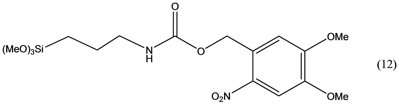
下記に記載する方法により、下記式(12)で表される4,5-ジメトキシ-2-ニトロベンジル(3-(トリメトキシシリル)プロピル)カルバメート(NBC-APTMOS)を合成した。
下記に記載する方法により、下記式(12)で表される4,5-ジメトキシ-2-ニトロベンジル(3-(トリメトキシシリル)プロピル)カルバメート(NBC-APTMOS)を合成した。
セプタム、三方コックを接続した3つ口丸底フラスコに窒素雰囲気下でクロロギ酸4,5-ジメトキシ-2-ニトロベンジル(シグマアルドリッチ、製品番号:420069)を4.00g(14.51mmol)量り入れ、無水THF(シグマアルドリッチ、製品番号401757)140mlを加え溶解させた。4-ジメチルアミノピリジン(東京化成工業、製品番号:D1450)を0.18g(1.45mmol)を量り入れ、室温で30分間撹拌した。3-アミノプロピルトリメトキシシラン(東京化成工業、製品番号:T1255)を5.20g(29.03mmol)、トリエチルアミン(和光純薬工業、製品番号:20-0264)を2.2g(21.77mmol)、無水THF(シグマアルドリッチ、製品番号401757)20mlに溶解させ滴下ロートを用いて溶液を0℃に冷却した反応器に滴下した。30分間撹拌した後、室温まで昇温し4時間撹拌を行った。反応液を10umのフィルターを用いてろ過し、トリエチルアミン塩酸を除去した。ろ液をロータリーエバポレーターおよび真空ポンプを用いて減圧乾燥させ粗生成物を8.26g得た。これをシリカゲルカラムクロマトグラフィを用いて精製し、下記式(12)で表される化合物を、黄色固体5.73g(13.68mmol、収率94%)で得た。
1H-NMR(ブルカーバイオスピン株式会社、AVANCEIII HD 500MHz),及びESI-MS(株式会社島津製作所、LCMS2020)の測定結果を以下に示す。
1H-NMR(500MHz,CDCl3):δ0.69(2H,t),1.64(2H,tt),3.29(2H,t),3.59(9H,s),4.03(6H,s),5.15(1H,br),5.52(2H,s),6.96(1H,s),7.78(1H,s)
ESI-MS:C16H27N2O9Si+(M+H+)の計算値m/z=419、実測値m/z=419
1H-NMR(500MHz,CDCl3):δ0.69(2H,t),1.64(2H,tt),3.29(2H,t),3.59(9H,s),4.03(6H,s),5.15(1H,br),5.52(2H,s),6.96(1H,s),7.78(1H,s)
ESI-MS:C16H27N2O9Si+(M+H+)の計算値m/z=419、実測値m/z=419
[感光性評価]
式(7)~(10)、(12)で表される化合物の其々に対し、UV-Vis分光光度計(株式会社島津製作所、UV-2450)を用いて、感光性の評価を行った。
式(7)~(10)、(12)で表される化合物の其々に対し、UV-Vis分光光度計(株式会社島津製作所、UV-2450)を用いて、感光性の評価を行った。
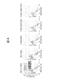
まず、式(7)~(10)、(12)で表される化合物を、クロロホルムまたはアセトニトリルに溶解して溶液試料を作成した。各試料に対するUV-Vis分光光度計での測定結果を、図4に示す。この結果から、350nm付近に吸収をもつ感光性脱離基が脱保護されアミンが発生すると共に、脱離した250nm付近に吸収を有するアルデヒドが生成していることがわかった。従って、本実施例1~4に記載のモノマー・ポリマー、及び比較例1に記載のシランカップリング剤共に、感光性のアミン発生剤として機能することが確認された。また、NMRによって反応率の定量変化を解析したところ、300mJ/cm2照射時の脱保護反応率はいずれも10%程度進行していることが確認され、高分子量化によって反応性が損失変化することはなかった。
[めっき配線の作製]
式(7)~(10)、(12)で表される化合物の其々を含む表面処理剤を用いて基板上に成膜し、めっき配線の作製を行った。
式(7)~(10)、(12)で表される化合物の其々を含む表面処理剤を用いて基板上に成膜し、めっき配線の作製を行った。
<実施例5>
実施例2で合成したP-NBC-AEMAにクロロホルムを加え、0.2wt%に調整した。この溶液を、PET基板(東洋紡績株式会社製、A-4100、コート無し)上にスピンコート(ミカサ株式会社製、MS-A150)3000rpm)にて塗布した。その後、105℃で10分乾燥させ、感光性ポリマー層を成膜した。
実施例2で合成したP-NBC-AEMAにクロロホルムを加え、0.2wt%に調整した。この溶液を、PET基板(東洋紡績株式会社製、A-4100、コート無し)上にスピンコート(ミカサ株式会社製、MS-A150)3000rpm)にて塗布した。その後、105℃で10分乾燥させ、感光性ポリマー層を成膜した。
次に、感光性ポリマー層を全面成膜した基板にフォトマスク(L/S=20μm/3mm)を介して、波長365nm光を300mJ/cm2露光して、感光性ポリマー層を感光させ、アミン発生層のパターンを形成した。次いで、無電解めっき用の触媒コロイド溶液(メルプレート アクチベーター7331、メルテックス社製)に、室温にて3分間浸漬し、アミン発生部に触媒(Pd)を付着させた。表面を水洗した後、無電解めっき液(メルプレートNI-867、メルテックス社製)に、73℃で1分間浸漬し、触媒上にニッケルリンを析出させて微細めっき配線を作製した。
<実施例6>
実施例5のP-NBC-AEMAを、実施例3で合成したP-NBC-AEMA-Allylに変えて、同様の処理を行い微細めっき配線を作製した。
実施例5のP-NBC-AEMAを、実施例3で合成したP-NBC-AEMA-Allylに変えて、同様の処理を行い微細めっき配線を作製した。
<実施例7>
実施例5のP-NBC-AEMAを、実施例3で合成したP-NBC-AEMA-TEOSに変えて、同様の処理を行い微細めっき配線を作製した。
実施例5のP-NBC-AEMAを、実施例3で合成したP-NBC-AEMA-TEOSに変えて、同様の処理を行い微細めっき配線を作製した。
<比較例2>
実施例5のP-NBC-AEMAを、実施例1で合成したNBC-AEMAに変えて、同様の処理を行い微細めっき配線を作製した。
実施例5のP-NBC-AEMAを、実施例1で合成したNBC-AEMAに変えて、同様の処理を行い微細めっき配線を作製した。
<比較例3>
実施例5のP-NBC-AEMAを、比較例1で合成したNBC-APTMOSに変えて、同様の処理を行い微細めっき配線を作製した。
実施例5のP-NBC-AEMAを、比較例1で合成したNBC-APTMOSに変えて、同様の処理を行い微細めっき配線を作製した。
[めっき配線及び溶解性の評価]
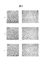
図5(a)に実施例5でめっき配線処理を行った、PET基板の全体写真と、光学顕微鏡(株式会社キーエンス製、VHX-900)像を示す。図5(b)に実施例6、図5(c)に実施例7で処理を行った同様のものを示した。
図5(a)に実施例5でめっき配線処理を行った、PET基板の全体写真と、光学顕微鏡(株式会社キーエンス製、VHX-900)像を示す。図5(b)に実施例6、図5(c)に実施例7で処理を行った同様のものを示した。
図示するように、実施例5~7において、105℃以下の低温プロセスにおいても、レジストを用いることなく細部に至るまで高精細の良好なめっき配線が形成されていることを、目視及び顕微鏡によって確認した。また、各層における剥離及び溶解は一切見られなかった。さらに、各化合物における溶媒への溶解性は易溶であり、その継時的変化も見られなかった。
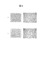
図6(a)に比較例2でめっき配線処理を行った、PET基板の全体写真と、光学顕微鏡(株式会社キーエンス製、VHX-900)像を示す。図6(b)に比較例3で処理を行った同様のものを示した。
図示するように、比較例2においては、選択的めっき配線は形成できなかった。そこで、溶液濃度を高めたところ、辛うじて成膜は確認できたが、めっき浴(70℃熱水)に曝した際に溶解・剥離することが確認された。これは、実施例1の材料が、シランカップリング剤のような密着性官能基を持たないため、基板への密着性が乏しく、感光性層が適切に形成されなかったためであると考えられる。
比較例3においては、選択的めっき配線は形成されていたものの、上記クロロホルム溶液において化合物が継時的に溶媒に難溶化し、最終的に不溶化することを目視で確認した。これは、加水分解の後縮合反応が進行し、アルコキシシラン同士の重合が進行したもの考えられる。
[表面平滑性の評価]
表面粗さ測定装置(ケーエルエー・テンコール株式会社製、P16)を用いて、スピンコート成膜後の基板の平滑性を測定した。PETの表面粗さRa値は2.78nmであるのに対し、実施例5~7で作製した成膜基板では、それぞれRa値は2.20nm、2.17nm、2.49nmであった。このことから、本発明の表面処理剤を用いれば、PET基板の平滑性を損なうことなく成膜が可能であることが確認できた。
表面粗さ測定装置(ケーエルエー・テンコール株式会社製、P16)を用いて、スピンコート成膜後の基板の平滑性を測定した。PETの表面粗さRa値は2.78nmであるのに対し、実施例5~7で作製した成膜基板では、それぞれRa値は2.20nm、2.17nm、2.49nmであった。このことから、本発明の表面処理剤を用いれば、PET基板の平滑性を損なうことなく成膜が可能であることが確認できた。
以上の結果から、本実施例の表面処理剤によれば、シランカップリング剤中のアルコキシシリル基のように基板や分子間での縮合を利用した密着機構を用いずとも、十分な密着性を得られた。また、アルコキシシリル基が存在しない、或いは殆ど存在しないことによって、所望の分子量まで高分子量化した後はそれ以上高分子量化することはなく、固体、溶液状態で既定の分子量を保持することができ、長期安定性を有し、可使時間の延命、再現性の高い成膜、膜自体の耐環境性向上が可能であった。これにより配線形成用フィルムの製造や運搬、またそれを用いた電子材料などの製造工程において管理の簡素化、コストの低減などが期待できる。
また、平滑基板に対し低温プロセスにおいてもレジストを用いることなく高精細な無電解めっき配線を施すことが可能であることが分かった。これにより例えば、多くの薬剤を使用する下地処理、レジスト現像、レジスト剥離工程や、エネルギーを必要とするPEBをはじめとする各工程での加熱工程が省略可能であり経済面、環境保全面で効果が期待できる。
さらに、本実施例を用いれば、安価に透明電極を作製できることが期待できる。これらを繰返し実施する電子デバイスなど多層配線形成を考えると、レジストフリープロセスによる効果は極めて大きいものである。また本発明により化学物質使用量の低減、短段階のデバイス製造プロセスを実現できれば量産性・経済性の向上効果だけではなく、製造装置開発及び維持に関る負担軽減を図ることができる。また、本発明によりもたらされる有機薄膜は2~10nm程度の極薄膜でも機能しており、極めて環境負荷が小さい。
11:基板、12:感光性ポリマー層、13:フォトマスク、14:アミン発生層、15:触媒層、16:めっき膜。
Claims (11)
- 下記式(1)で表される構成単位を有する高分子化合物。

〔式(1)中、R1は水素またはメチル基を表し、mは2~20の整数を表し、Qは感光性脱離基を表す。〕 - 請求項1に記載の高分子化合物であって、Qは、少なくとも一種の下記式(2)で表される基であることを特徴とする高分子化合物。
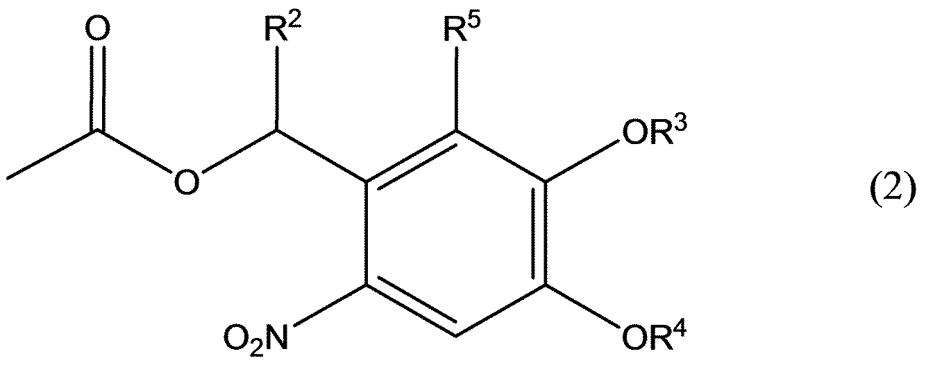
〔式(2)中、R2は水素またはアルキル基を表し、R3及びR4はそれぞれ独立してメチル基を含むアルキル基またはフルオロアルキル基を表し、R5は水素またはニトロ基を表す。〕 - 請求項1または2に記載の高分子化合物であって、
式(1)で表される化合物の数平均分子量が、1000~5000である
ことを特徴とする高分子化合物。 - 請求項1から3の何れか一項に記載の高分子化合物であって、
アルコキシシランを含まないこと
を特徴とする高分子化合物。 - 請求項1から4の何れか一項に記載の高分子化合物であって、
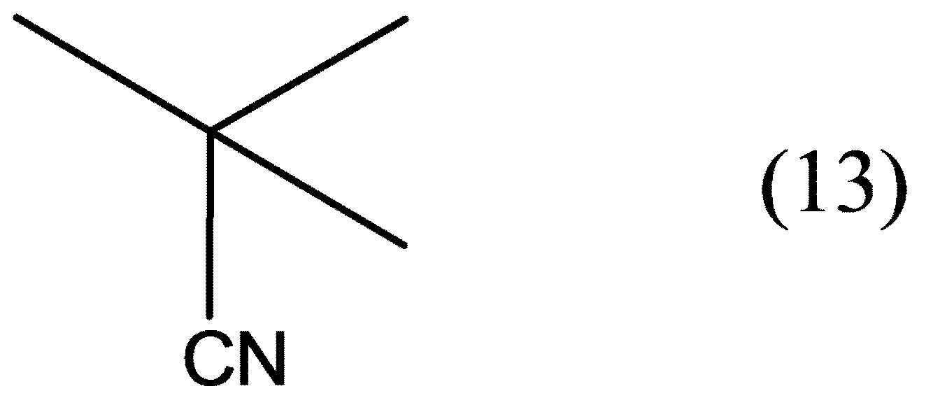
式(1)で表される化合物の少なくとも1つの末端が、下記一般式(13)で表される置換基である
ことを特徴とする高分子化合物。
- 請求項1から4の何れか一項に記載の高分子化合物であって、
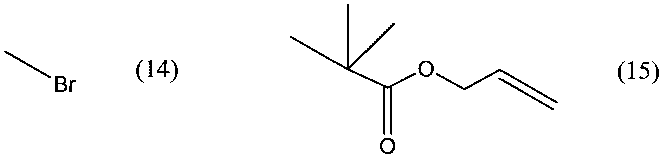
式(1)で表される化合物の末端が、下記式(14)及び下記式(15)で表される置換基である
ことを特徴とする高分子化合物。
- 請求項1から3の何れか一項に記載の高分子化合物であって、
式(1)で表される化合物の末端が、下記式(16)及び下記式(17)で表される置換基である
ことを特徴とする高分子化合物。

- 請求項1から7の何れか一項に記載の高分子化合物を含む表面処理剤。
- 請求項8に記載の表面処理剤を含む積層体。
- 請求項8に記載の表面処理剤を含むトランジスタ。
- 積層体の製造方法であって、
請求項8に記載の表面処理剤を塗布して感光性ポリマー層を形成する工程と、
前記感光性ポリマー層を所定のパターン光で露光する工程と、
前記感光性ポリマー層の前記露光された領域に無電解めっき用触媒を付与する工程と、
前記感光性ポリマー層を無電解めっき液に接触させて無電解めっきを行う工程と、
を有する積層体の製造方法。
Priority Applications (3)
| Application Number | Priority Date | Filing Date | Title |
|---|---|---|---|
| JP2017511097A JP6724903B2 (ja) | 2015-04-10 | 2016-04-08 | 高分子化合物、表面処理剤、表面処理剤を用いた積層体、トランジスタ、積層体の製造方法 |
| CN201680006157.2A CN107108796B (zh) | 2015-04-10 | 2016-04-08 | 高分子化合物、表面处理剂、使用表面处理剂的层积体、晶体管、层积体的制造方法 |
| US15/659,838 US10550281B2 (en) | 2015-04-10 | 2017-07-26 | Polymer compound, surface treatment agent, laminated body using surface treatment agent, transistor, method for manufacturing laminated body |
Applications Claiming Priority (2)
| Application Number | Priority Date | Filing Date | Title |
|---|---|---|---|
| JP2015-081164 | 2015-04-10 | ||
| JP2015081164 | 2015-04-10 |
Related Child Applications (1)
| Application Number | Title | Priority Date | Filing Date |
|---|---|---|---|
| US15/659,838 Continuation US10550281B2 (en) | 2015-04-10 | 2017-07-26 | Polymer compound, surface treatment agent, laminated body using surface treatment agent, transistor, method for manufacturing laminated body |
Publications (1)
| Publication Number | Publication Date |
|---|---|
| WO2016163525A1 true WO2016163525A1 (ja) | 2016-10-13 |
Family
ID=57071997
Family Applications (1)
| Application Number | Title | Priority Date | Filing Date |
|---|---|---|---|
| PCT/JP2016/061571 Ceased WO2016163525A1 (ja) | 2015-04-10 | 2016-04-08 | 高分子化合物、表面処理剤、表面処理剤を用いた積層体、トランジスタ、積層体の製造方法 |
Country Status (4)
| Country | Link |
|---|---|
| US (1) | US10550281B2 (ja) |
| JP (1) | JP6724903B2 (ja) |
| CN (1) | CN107108796B (ja) |
| WO (1) | WO2016163525A1 (ja) |
Cited By (3)
| Publication number | Priority date | Publication date | Assignee | Title |
|---|---|---|---|---|
| WO2024043221A1 (ja) * | 2022-08-22 | 2024-02-29 | 株式会社ニコン | 感光性表面処理剤、パターン形成用基板、積層体、トランジスタ、パターン形成方法及びトランジスタの製造方法 |
| WO2024043222A1 (ja) * | 2022-08-22 | 2024-02-29 | 株式会社ニコン | 感光性表面処理剤、積層体、パターン形成用基板、トランジスタ、パターン形成方法及びトランジスタの製造方法 |
| WO2025069203A1 (ja) * | 2023-09-26 | 2025-04-03 | 株式会社ニコン | 積層体、トランジスタ、積層体の製造方法及びトランジスタの製造方法 |
Citations (5)
| Publication number | Priority date | Publication date | Assignee | Title |
|---|---|---|---|---|
| JP2002265531A (ja) * | 2001-03-13 | 2002-09-18 | Kunihiro Ichimura | 塩基増殖性不飽和化合物、塩基増殖性樹脂及び該樹脂を含む組成物 |
| JP2006251478A (ja) * | 2005-03-11 | 2006-09-21 | Toyobo Co Ltd | ポジ型感光性ポリイミド前駆体組成物 |
| WO2012105321A1 (ja) * | 2011-02-03 | 2012-08-09 | 株式会社クラレ | アクリル酸エステル誘導体、高分子化合物およびフォトレジスト組成物 |
| JP2013149860A (ja) * | 2012-01-20 | 2013-08-01 | Sumitomo Chemical Co Ltd | 有機薄膜トランジスタ絶縁層材料 |
| WO2013151739A1 (en) * | 2012-04-03 | 2013-10-10 | 3M Innovative Properties Company | Crosslinkable composition comprising photobase generators |
Family Cites Families (2)
| Publication number | Priority date | Publication date | Assignee | Title |
|---|---|---|---|---|
| JPH08146608A (ja) * | 1994-11-16 | 1996-06-07 | Hitachi Ltd | 感光性樹脂組成物とそれを用いた電子装置の製法 |
| JP3634658B2 (ja) | 1999-03-08 | 2005-03-30 | キヤノン株式会社 | パターン基板、およびその製造方法 |
-
2016
- 2016-04-08 CN CN201680006157.2A patent/CN107108796B/zh active Active
- 2016-04-08 JP JP2017511097A patent/JP6724903B2/ja active Active
- 2016-04-08 WO PCT/JP2016/061571 patent/WO2016163525A1/ja not_active Ceased
-
2017
- 2017-07-26 US US15/659,838 patent/US10550281B2/en active Active
Patent Citations (5)
| Publication number | Priority date | Publication date | Assignee | Title |
|---|---|---|---|---|
| JP2002265531A (ja) * | 2001-03-13 | 2002-09-18 | Kunihiro Ichimura | 塩基増殖性不飽和化合物、塩基増殖性樹脂及び該樹脂を含む組成物 |
| JP2006251478A (ja) * | 2005-03-11 | 2006-09-21 | Toyobo Co Ltd | ポジ型感光性ポリイミド前駆体組成物 |
| WO2012105321A1 (ja) * | 2011-02-03 | 2012-08-09 | 株式会社クラレ | アクリル酸エステル誘導体、高分子化合物およびフォトレジスト組成物 |
| JP2013149860A (ja) * | 2012-01-20 | 2013-08-01 | Sumitomo Chemical Co Ltd | 有機薄膜トランジスタ絶縁層材料 |
| WO2013151739A1 (en) * | 2012-04-03 | 2013-10-10 | 3M Innovative Properties Company | Crosslinkable composition comprising photobase generators |
Cited By (6)
| Publication number | Priority date | Publication date | Assignee | Title |
|---|---|---|---|---|
| WO2024043221A1 (ja) * | 2022-08-22 | 2024-02-29 | 株式会社ニコン | 感光性表面処理剤、パターン形成用基板、積層体、トランジスタ、パターン形成方法及びトランジスタの製造方法 |
| WO2024043222A1 (ja) * | 2022-08-22 | 2024-02-29 | 株式会社ニコン | 感光性表面処理剤、積層体、パターン形成用基板、トランジスタ、パターン形成方法及びトランジスタの製造方法 |
| JP2024029570A (ja) * | 2022-08-22 | 2024-03-06 | 株式会社ニコン | 感光性表面処理剤、パターン形成用基板、積層体、トランジスタ、パターン形成方法及びトランジスタの製造方法 |
| JP2024029569A (ja) * | 2022-08-22 | 2024-03-06 | 株式会社ニコン | 感光性表面処理剤、積層体、パターン形成用基板、トランジスタ、パターン形成方法及びトランジスタの製造方法 |
| WO2025069203A1 (ja) * | 2023-09-26 | 2025-04-03 | 株式会社ニコン | 積層体、トランジスタ、積層体の製造方法及びトランジスタの製造方法 |
| WO2025069828A1 (ja) * | 2023-09-26 | 2025-04-03 | 株式会社ニコン | 積層体、トランジスタ、積層体の製造方法及びトランジスタの製造方法 |
Also Published As
| Publication number | Publication date |
|---|---|
| US10550281B2 (en) | 2020-02-04 |
| US20170321079A1 (en) | 2017-11-09 |
| JP6724903B2 (ja) | 2020-07-15 |
| CN107108796B (zh) | 2019-10-01 |
| CN107108796A (zh) | 2017-08-29 |
| JPWO2016163525A1 (ja) | 2018-02-01 |
Similar Documents
| Publication | Publication Date | Title |
|---|---|---|
| CN105198916B (zh) | 官能化双塔型多面体低聚倍半硅氧烷及其制备方法 | |
| KR20160118340A (ko) | 교차-결합 가능한 플루오르화된 포토폴리머 | |
| CN108884568B (zh) | 导电性层叠体的制造方法、层叠体及导电性层叠体 | |
| JP6724903B2 (ja) | 高分子化合物、表面処理剤、表面処理剤を用いた積層体、トランジスタ、積層体の製造方法 | |
| TWI758475B (zh) | 活性能量線硬化型組成物、硬化膜的製造方法及硬化物 | |
| US20250180990A1 (en) | Photosensitive surface treating agent, laminate, pattern formation substrate, transistor, pattern forming method and method of producing transistor | |
| JP2011079877A (ja) | 高分子超薄膜および高分子超薄膜パターン、並びに、パターン形成用組成物 | |
| US9081283B2 (en) | Spatial and temporal control of brush formation on surfaces | |
| CN107532302B (zh) | 感光性非电解镀基底剂 | |
| JP7116941B2 (ja) | ブロック共重合体及び相分離構造を含む構造体の製造方法 | |
| TW202444801A (zh) | 感光性樹脂組成物、硬化物、積層體、硬化物的製造方法、積層體的製造方法、半導體元件的製造方法及半導體元件 | |
| CN109963658A (zh) | 图案形成方法、底涂剂和层压体 | |
| US9534134B2 (en) | Agent for the surface epilamization of an article | |
| WO2023033146A1 (ja) | 成膜基板 | |
| US9069248B1 (en) | Forming conductive metal patterns using water-soluble copolymers | |
| US9389512B2 (en) | Forming conductive metal patterns using water-soluble polymers | |
| JP7308474B2 (ja) | 特殊構造パターンを創出するブロック共重合体の製造方法 | |
| CN121889402A (zh) | 化合物、感光性表面处理剂、层叠体的制造方法及晶体管的制造方法 | |
| JP2021092758A (ja) | ネガ型感光性樹脂組成物及び硬化膜の製造方法 | |
| US9128378B2 (en) | Forming conductive metal patterns with reactive polymers | |
| WO2015069475A1 (en) | Forming conductive metal patterns using reactive polymers | |
| JP4566577B2 (ja) | ポリシルセスキオキサングラフト重合体、その製造方法及び粘着剤 | |
| US9316914B2 (en) | Electroless plating method using non-reducing agent | |
| US9329481B2 (en) | Electroless plating method using halide | |
| WO2008038500A1 (en) | Laminate, method of forming conductive pattern, conductive pattern obtained thereby, printed wiring board, thin-layer transistor and apparatus utilizing these |
Legal Events
| Date | Code | Title | Description |
|---|---|---|---|
| 121 | Ep: the epo has been informed by wipo that ep was designated in this application |
Ref document number: 16776691 Country of ref document: EP Kind code of ref document: A1 |
|
| ENP | Entry into the national phase |
Ref document number: 2017511097 Country of ref document: JP Kind code of ref document: A |
|
| NENP | Non-entry into the national phase |
Ref country code: DE |
|
| 122 | Ep: pct application non-entry in european phase |
Ref document number: 16776691 Country of ref document: EP Kind code of ref document: A1 |