WO2016158090A1 - 半導体発光素子及びその製造方法 - Google Patents
半導体発光素子及びその製造方法 Download PDFInfo
- Publication number
- WO2016158090A1 WO2016158090A1 PCT/JP2016/055168 JP2016055168W WO2016158090A1 WO 2016158090 A1 WO2016158090 A1 WO 2016158090A1 JP 2016055168 W JP2016055168 W JP 2016055168W WO 2016158090 A1 WO2016158090 A1 WO 2016158090A1
- Authority
- WO
- WIPO (PCT)
- Prior art keywords
- layer
- light emitting
- type semiconductor
- semiconductor layer
- protective layer
- Prior art date
- Legal status (The legal status is an assumption and is not a legal conclusion. Google has not performed a legal analysis and makes no representation as to the accuracy of the status listed.)
- Ceased
Links
Images








Classifications
-
- H—ELECTRICITY
- H10—SEMICONDUCTOR DEVICES; ELECTRIC SOLID-STATE DEVICES NOT OTHERWISE PROVIDED FOR
- H10P—GENERIC PROCESSES OR APPARATUS FOR THE MANUFACTURE OR TREATMENT OF DEVICES COVERED BY CLASS H10
- H10P14/00—Formation of materials, e.g. in the shape of layers or pillars
- H10P14/20—Formation of materials, e.g. in the shape of layers or pillars of semiconductor materials
- H10P14/29—Formation of materials, e.g. in the shape of layers or pillars of semiconductor materials characterised by the substrates
- H10P14/2901—Materials
- H10P14/2921—Materials being crystalline insulating materials
-
- H—ELECTRICITY
- H10—SEMICONDUCTOR DEVICES; ELECTRIC SOLID-STATE DEVICES NOT OTHERWISE PROVIDED FOR
- H10H—INORGANIC LIGHT-EMITTING SEMICONDUCTOR DEVICES HAVING POTENTIAL BARRIERS
- H10H20/00—Individual inorganic light-emitting semiconductor devices having potential barriers, e.g. light-emitting diodes [LED]
- H10H20/80—Constructional details
- H10H20/81—Bodies
- H10H20/811—Bodies having quantum effect structures or superlattices, e.g. tunnel junctions
- H10H20/812—Bodies having quantum effect structures or superlattices, e.g. tunnel junctions within the light-emitting regions, e.g. having quantum confinement structures
-
- H—ELECTRICITY
- H10—SEMICONDUCTOR DEVICES; ELECTRIC SOLID-STATE DEVICES NOT OTHERWISE PROVIDED FOR
- H10H—INORGANIC LIGHT-EMITTING SEMICONDUCTOR DEVICES HAVING POTENTIAL BARRIERS
- H10H20/00—Individual inorganic light-emitting semiconductor devices having potential barriers, e.g. light-emitting diodes [LED]
- H10H20/80—Constructional details
- H10H20/81—Bodies
- H10H20/819—Bodies characterised by their shape, e.g. curved or truncated substrates
-
- H—ELECTRICITY
- H10—SEMICONDUCTOR DEVICES; ELECTRIC SOLID-STATE DEVICES NOT OTHERWISE PROVIDED FOR
- H10P—GENERIC PROCESSES OR APPARATUS FOR THE MANUFACTURE OR TREATMENT OF DEVICES COVERED BY CLASS H10
- H10P14/00—Formation of materials, e.g. in the shape of layers or pillars
- H10P14/20—Formation of materials, e.g. in the shape of layers or pillars of semiconductor materials
- H10P14/24—Formation of materials, e.g. in the shape of layers or pillars of semiconductor materials using chemical vapour deposition [CVD]
-
- H—ELECTRICITY
- H10—SEMICONDUCTOR DEVICES; ELECTRIC SOLID-STATE DEVICES NOT OTHERWISE PROVIDED FOR
- H10P—GENERIC PROCESSES OR APPARATUS FOR THE MANUFACTURE OR TREATMENT OF DEVICES COVERED BY CLASS H10
- H10P14/00—Formation of materials, e.g. in the shape of layers or pillars
- H10P14/20—Formation of materials, e.g. in the shape of layers or pillars of semiconductor materials
- H10P14/32—Formation of materials, e.g. in the shape of layers or pillars of semiconductor materials characterised by intermediate layers between substrates and deposited layers
- H10P14/3202—Materials thereof
- H10P14/3214—Materials thereof being Group IIIA-VA semiconductors
- H10P14/3216—Nitrides
-
- H—ELECTRICITY
- H10—SEMICONDUCTOR DEVICES; ELECTRIC SOLID-STATE DEVICES NOT OTHERWISE PROVIDED FOR
- H10P—GENERIC PROCESSES OR APPARATUS FOR THE MANUFACTURE OR TREATMENT OF DEVICES COVERED BY CLASS H10
- H10P14/00—Formation of materials, e.g. in the shape of layers or pillars
- H10P14/20—Formation of materials, e.g. in the shape of layers or pillars of semiconductor materials
- H10P14/32—Formation of materials, e.g. in the shape of layers or pillars of semiconductor materials characterised by intermediate layers between substrates and deposited layers
- H10P14/3242—Structure
- H10P14/3244—Layer structure
- H10P14/3251—Layer structure consisting of three or more layers
-
- H—ELECTRICITY
- H10—SEMICONDUCTOR DEVICES; ELECTRIC SOLID-STATE DEVICES NOT OTHERWISE PROVIDED FOR
- H10P—GENERIC PROCESSES OR APPARATUS FOR THE MANUFACTURE OR TREATMENT OF DEVICES COVERED BY CLASS H10
- H10P14/00—Formation of materials, e.g. in the shape of layers or pillars
- H10P14/20—Formation of materials, e.g. in the shape of layers or pillars of semiconductor materials
- H10P14/34—Deposited materials, e.g. layers
- H10P14/3402—Deposited materials, e.g. layers characterised by the chemical composition
- H10P14/3414—Deposited materials, e.g. layers characterised by the chemical composition being group IIIA-VIA materials
- H10P14/3416—Nitrides
-
- H—ELECTRICITY
- H10—SEMICONDUCTOR DEVICES; ELECTRIC SOLID-STATE DEVICES NOT OTHERWISE PROVIDED FOR
- H10P—GENERIC PROCESSES OR APPARATUS FOR THE MANUFACTURE OR TREATMENT OF DEVICES COVERED BY CLASS H10
- H10P14/00—Formation of materials, e.g. in the shape of layers or pillars
- H10P14/20—Formation of materials, e.g. in the shape of layers or pillars of semiconductor materials
- H10P14/34—Deposited materials, e.g. layers
- H10P14/3438—Doping during depositing
- H10P14/3441—Conductivity type
- H10P14/3442—N-type
-
- H—ELECTRICITY
- H10—SEMICONDUCTOR DEVICES; ELECTRIC SOLID-STATE DEVICES NOT OTHERWISE PROVIDED FOR
- H10P—GENERIC PROCESSES OR APPARATUS FOR THE MANUFACTURE OR TREATMENT OF DEVICES COVERED BY CLASS H10
- H10P14/00—Formation of materials, e.g. in the shape of layers or pillars
- H10P14/20—Formation of materials, e.g. in the shape of layers or pillars of semiconductor materials
- H10P14/34—Deposited materials, e.g. layers
- H10P14/3438—Doping during depositing
- H10P14/3441—Conductivity type
- H10P14/3444—P-type
-
- H—ELECTRICITY
- H10—SEMICONDUCTOR DEVICES; ELECTRIC SOLID-STATE DEVICES NOT OTHERWISE PROVIDED FOR
- H10P—GENERIC PROCESSES OR APPARATUS FOR THE MANUFACTURE OR TREATMENT OF DEVICES COVERED BY CLASS H10
- H10P14/00—Formation of materials, e.g. in the shape of layers or pillars
- H10P14/20—Formation of materials, e.g. in the shape of layers or pillars of semiconductor materials
- H10P14/36—Formation of materials, e.g. in the shape of layers or pillars of semiconductor materials characterised by treatments done before the formation of the materials
-
- H—ELECTRICITY
- H10—SEMICONDUCTOR DEVICES; ELECTRIC SOLID-STATE DEVICES NOT OTHERWISE PROVIDED FOR
- H10H—INORGANIC LIGHT-EMITTING SEMICONDUCTOR DEVICES HAVING POTENTIAL BARRIERS
- H10H20/00—Individual inorganic light-emitting semiconductor devices having potential barriers, e.g. light-emitting diodes [LED]
- H10H20/01—Manufacture or treatment
- H10H20/011—Manufacture or treatment of bodies, e.g. forming semiconductor layers
- H10H20/013—Manufacture or treatment of bodies, e.g. forming semiconductor layers having light-emitting regions comprising only Group III-V materials
- H10H20/0133—Manufacture or treatment of bodies, e.g. forming semiconductor layers having light-emitting regions comprising only Group III-V materials with a substrate not being Group III-V materials
- H10H20/01335—Manufacture or treatment of bodies, e.g. forming semiconductor layers having light-emitting regions comprising only Group III-V materials with a substrate not being Group III-V materials the light-emitting regions comprising nitride materials
-
- H—ELECTRICITY
- H10—SEMICONDUCTOR DEVICES; ELECTRIC SOLID-STATE DEVICES NOT OTHERWISE PROVIDED FOR
- H10H—INORGANIC LIGHT-EMITTING SEMICONDUCTOR DEVICES HAVING POTENTIAL BARRIERS
- H10H20/00—Individual inorganic light-emitting semiconductor devices having potential barriers, e.g. light-emitting diodes [LED]
- H10H20/80—Constructional details
- H10H20/81—Bodies
- H10H20/822—Materials of the light-emitting regions
- H10H20/824—Materials of the light-emitting regions comprising only Group III-V materials, e.g. GaP
- H10H20/825—Materials of the light-emitting regions comprising only Group III-V materials, e.g. GaP containing nitrogen, e.g. GaN
- H10H20/8252—Materials of the light-emitting regions comprising only Group III-V materials, e.g. GaP containing nitrogen, e.g. GaN characterised by the dopants
Definitions
- the present invention relates to a semiconductor light emitting device having an active layer in which light emitting layers and barrier layers are alternately stacked between an n-type semiconductor layer and a p-type semiconductor layer, and a method for manufacturing the same.
- Semiconductor light-emitting elements that emit ultraviolet light have a wide range of application products such as exposure, curing, sterilization, medical care, and sensor applications, and a large market is expected in the future.
- a conventional InGaN-based semiconductor light-emitting device has an n-type semiconductor layer, an active layer in which barrier layers and light-emitting layers are alternately stacked, and a p-type semiconductor layer on a growth substrate made of sapphire or the like. It is the mainstream that is made by growing a semiconductor layer and bonding the semiconductor layer on the growth substrate and the supporting substrate using solder applied on the substrate and then peeling the growth substrate by laser lift-off. .
- InGaN-based semiconductor light-emitting devices that are currently popular are formed by epitaxially growing a GaN layer and an InGaN layer on a sapphire substrate. At this time, since sapphire and GaN and InGaN have different lattice constants, it is known that crystal defects called high-density dislocations exist in the growth layer (see, for example, Patent Documents 1 and 2).
- the epitaxial layer thereon can also have a low dislocation density as in the substrate.
- the wavelength of laser light used for laser lift-off is mainly 300 nm or less.
- this laser light does not pass through the GaN substrate, it is difficult to peel off the GaN substrate.
- a sapphire substrate is mainly used as a growth substrate.
- the InGaN-based semiconductor light-emitting device has a GaN layer and an InGaN layer grown epitaxially on a sapphire substrate having a different lattice constant, a crystal defect called dislocation exists.
- the present inventor has found that leaks are generated due to this dislocation and the device characteristics (for example, Ir characteristics) of the semiconductor light emitting device are deteriorated through intensive studies.
- FIG. 1 is a photograph showing a state of light emission when a minute current is passed between a p-side pad electrode 61 and an n-side pad electrode 62 with respect to an InGaN-based semiconductor light-emitting device 60 manufactured by a conventional method.
- the initial stage no light emission spots are observed, but when the amount of supplied current is gradually increased, spots 63 that emit light blue and white are scattered. In particular, many light emitting portions 63 appear around the p-side pad electrode 61.
- FIG. 2 is a photograph of a cross-section of the semiconductor light emitting element 60 at one light emitting point 63 taken with a TEM (Transmission Electron Microscope).
- (B) is an enlargement of (a).
- FIG. 2B is an enlarged view of the location where the active layer 67 and the p-type semiconductor layer 68 are formed, and it can be seen that the dislocation 65 is generated at this location.
- the present inventor has inferred that the reason why the Ir characteristics of the semiconductor light emitting device 60 manufactured by the conventional method are deteriorated is due to the occurrence of leakage due to the dislocation 65.
- some pit (concave portion) is formed due to the dislocation 65, and Mg, which is a p-type impurity contained in the p-type semiconductor layer 68, is transferred to the active layer 67 and the n-type semiconductor layer via the pit.
- Mg which is a p-type impurity contained in the p-type semiconductor layer 68
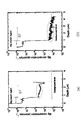
- FIG. 3 is a graph in which the Mg concentration in the depth direction was measured by SIMS (Secondary Ion Mass Spectrometry) for two InGaN-based semiconductor light-emitting devices having different dislocation densities (the above non-explanatory).
- Patent Document 1 a graph showing the result of a device having a dislocation density of the order of 1 ⁇ 10 9 / cm 2
- (b) shows the result of a device having a dislocation density of 6 ⁇ 10 7 / cm 2. It is a graph to show.
- the Mg signal due to the p-type semiconductor layer 68 appears in the vicinity of the depth of 1 ⁇ m to 2.5 ⁇ m in the result of (a). This is because Mg penetrates into the active layer 67. Suggests that On the other hand, in the result of (b), it can be seen that Mg remains at the detection limit value (background level) at the position of the active layer 67 and Mg does not penetrate into the active layer 67. In other words, it can be seen that Mg diffuses into the active layer 67 from the p-type semiconductor layer 68 side in the element having a high dislocation density.
- FIG. 4 is a SEM photograph of the surface state immediately after the formation of the active layer 67 in the InGaN-based semiconductor light emitting device 60 having the same configuration as the conventional one.
- FIG. 5 is a schematic diagram showing a cross-sectional structure of the element in the state of FIG.
- a sapphire substrate is used as the growth substrate 11, and after the undoped layer 13 and the n-type semiconductor layer 21 are grown on the growth substrate 11, the barrier layer 25 (25a, 25b made of an AlGaN layer having a thickness of 20 nm is formed.
- the barrier layer 25f corresponds to the final barrier layer.
- the flow rate of trimethylaluminum (TMA) is 1.6 ⁇ mol / min and the flow rate of trimethylgallium (TMG) is 10 ⁇ mol / min.
- photographed the surface state in the state which lowered temperature to room temperature, without forming a p-type semiconductor layer is FIG.
- FIG. 4 confirms that a plurality of pits (concave portions) 71 are formed on the surface of the final barrier layer 25f.
- the diameter (diameter) of the pit 71 is estimated to be approximately 70 to 90 nm, and in view of the fact that the tilt angle of the azimuth plane where crystallization is likely to occur stably in the GaN system is about 60 °, It is presumed that the diameter and depth of 71 are almost equal.
- the thickness of each light emitting layer 23 is 10 nm and the thickness of each barrier layer 25 is 20 nm
- the pits 71 are the light emitting layer 23e, the barrier layer 25e, and the light emitting layer 23d located below the final barrier layer 25f. It is estimated that the barrier layer reaches about 25d. In FIG. 5, such a state of the pit 71 is schematically displayed.
- FIG. 6 shows an InGaN-based semiconductor light emitting device similar to the conventional one, after forming the active layer 67 at a temperature of 820 ° C., the temperature is raised to 1025 ° C., which is the temperature for growing the p-type semiconductor layer 68 in 2 minutes.
- 5 is an SEM photograph of the surface state taken when the temperature is lowered to room temperature without growing the p-type semiconductor layer 68.
- 6A and 6B similarly to FIG. 4, FIG. 6A shows a photograph with a magnification of 10,000 times, and FIG. 6B shows a photograph with a magnification of 100,000 times.
- FIG. 7 is a schematic diagram showing a cross-sectional structure of the element in the state of FIG.
- the diameter (diameter) of the pit 71 is estimated to be approximately 20 to 40 nm, and it can be seen that the diameter of the pit 71 is smaller than that in the state of FIG. This is because, as the temperature increases, the epitaxial growth mode changes from the mode growing in the vertical direction to the mode growing in the horizontal direction, that is, the mode in which the pits 71 are embedded. It is presumed that the depth has decreased. More specifically, while the temperature is raised, the raw material on the surface of the layer maintaining thermal equilibrium is etched and moved, and the etched material and the gas in the furnace enter the pit 71 and grow in the horizontal direction. Thus, it is considered that a part of the pit 71 (region 71a in FIG. 7) is filled.
- the depth of the pit 71 in FIG. 6 is estimated to be about 20 to 40 nm, so the pit 71 is located below the final barrier layer 25f. It reaches the light emitting layer 23e, and it is considered that some pits 71 also reach the barrier layer 25e.
- the p-type impurities contained in the p-type semiconductor layer 68 reach the light emitting layer 23e through the pits 71, and some of the p-type impurities are further added to the light emitting layer 23e. It is considered that the lower barrier layer 25e is reached.
- the present inventor has found that a p-type impurity penetrates into the active layer 67 due to the presence of the pit 71 and the pn junction is destroyed, so that a leak current as shown in the photograph of FIG. 1 is generated. I figured out what I was doing.
- an object of the present invention is to realize a semiconductor light emitting device that suppresses the generation of leakage current and enhances light emission efficiency.
- the present invention is a semiconductor light emitting device having an active layer in which light emitting layers and barrier layers are alternately stacked between an n-type semiconductor layer and a p-type semiconductor layer, An upper surface of a final barrier layer formed on the side of the barrier layer closest to the p-type semiconductor layer is a layer different from the final barrier layer and has a p-type impurity concentration higher than that of the p-type semiconductor layer.
- a pit (concave portion) reaches the light emitting layer constituting the active layer immediately before forming the p-type semiconductor layer, and the p-type is formed through this pit. It is considered that a leak current was generated as a result of the impurities entering the light emitting layer.
- the tip of the pit formed at the time of manufacture is kept at the height position of the protective layer or the height position of the final barrier layer, and the state where it does not reach the light emitting layer located therebelow. Can be realized.
- the frequency can be greatly reduced as compared with the conventional case. Thereby, leakage current can be suppressed more than before. This result will be described later with reference to an example.
- this protective layer is formed as an undoped layer at the time of manufacture, it is exposed to a high temperature (for example, about 1000 ° C.) in the process of forming a p-type semiconductor layer on the upper surface of this protective layer.
- a p-type impurity may be diffused from the p-type semiconductor layer to form a layer containing a low-concentration p-type impurity.
- the p-type impurity concentration contained in the protective layer may have a distribution in the thickness direction.
- this protective layer may be a layer formed at the time of manufacture as a layer containing a low concentration of n-type impurities or a layer containing a very low concentration of p-type impurities.
- the concentration of the p-type impurity contained in the p-type semiconductor layer is, for example, higher than 1 ⁇ 10 19 / cm 3 , and preferably about 2 to 3 ⁇ 10 19 / cm 3 .
- the concentration of the p-type impurity contained in the protective layer can be 1 ⁇ 10 19 / cm 3 or less, preferably 1 ⁇ 10 18 / cm 3 or less.
- the p-type semiconductor layer penetrates into the protective layer, and the tip is at a height position on the upper surface of the light emitting layer formed on the n-type semiconductor layer side with respect to the final barrier layer. It can be set as the structure which has the protrusion part which has not reached.
- the protective layer By forming the protective layer on the upper surface of the final barrier layer, even if pits appear on the surface of the final barrier layer at the time when the final barrier layer is formed, at least a part of the inside of the pit is removed. It can be filled with a protective layer. In particular, by filling the tip of the pit that has reached the light emitting layer with the protective layer, the state where the tip of the pit does not reach the height position of the upper surface of the light emitting layer at the time after forming the protective layer is realized. . By forming the p-type semiconductor layer under such a state, even if pits exist at the start of formation of the p-type semiconductor layer, the pits have reached the height position on the upper surface of the light emitting layer. Therefore, it is possible to suppress the p-type impurity doped in the p-type semiconductor layer from diffusing into the light emitting layer.
- the protruding portion is formed by the diffusion of the p-type impurity contained in the p-type semiconductor layer into the pit (recess) formed in the protective layer immediately before forming the p-type semiconductor layer. It does n’t matter. Since the tip of the projecting portion does not reach the height position of the upper surface of the light emitting layer, a situation in which p-type impurities diffuse into the active layer and the pn junction is broken is avoided.
- the tip of the pit formed at the time before the formation of the protective layer is filled so that the tip of the pit remaining at the time after the formation of the protective layer is higher than the upper surface of the light emitting layer. It is sufficient that the thickness is not less than the minimum film thickness necessary for realizing a state where the position is not reached.
- the protective layer may be formed of a thin film than the final barrier layer.
- the thickness of the protective layer is increased, the distance between the p-type impurity layer and the light-emitting layer is increased, so that holes supplied from the p-type semiconductor layer are difficult to reach the light-emitting layer.
- electrons are confined at the interface between the final barrier layer and the p-type semiconductor layer, and an impurity level may be formed to emit light having a wavelength different from the desired wavelength.
- an impurity level may be formed to emit light having a wavelength different from the desired wavelength.
- the protective layer is preferably as thin as possible, having a thickness equal to or greater than the minimum film thickness.
- This temperature condition is higher than the growth temperature of the active layer including the final barrier layer, and can be, for example, 1000 ° C. or higher.
- the p-type semiconductor layer may contain Mg as a p-type impurity.
- FIG. 8 shows Ir (reverse current) when a reverse bias is applied when the formation conditions of the p-type semiconductor layer 68 formed above the final barrier layer 25f are changed for an InGaN-based semiconductor light-emitting device manufactured by a conventional method. ) Is a graph showing characteristics.
- Cp 2 Mg biscyclopentadienyl magnesium
- the effect of suppressing the leakage current is greatly exhibited by using the semiconductor light-emitting element including the protective layer as described above.
- the method for manufacturing the semiconductor light emitting device of the present invention includes: Forming an n-type semiconductor layer on the substrate (a); (B) forming an active layer by alternately laminating light emitting layers and barrier layers on the n-type semiconductor layer; (C) forming a protective layer different from the final barrier layer on the upper surface of the final barrier layer formed on the side of the barrier layer closest to the p-type semiconductor layer; supplying a p-type dopant to form a p-type semiconductor layer on the upper surface of the protective layer (d), In the step (c), at least a part of the pit so that the tip of the pit that appears on the uppermost surface of the layer before the start of the step (c) does not reach at least the height position of the light emitting layer. Is filled with the protective layer.
- the tip of the pit formed in the layer is left in the protective layer or the final barrier layer and is formed in the lower layer.
- the state where the height of the light emitting layer is not reached is realized.
- the p-type impurity diffuses to the protective layer or the final barrier layer through the pits, but does not diffuse to the underlying light emitting layer.
- the pn junction is not destroyed and the occurrence of leakage current is suppressed.
- the step (c) can be a step of forming the protective layer by growing a predetermined semiconductor layer under a temperature condition capable of lateral growth.
- This temperature condition is higher than the growth temperature of the active layer including the final barrier layer, and can be, for example, 1000 ° C. or higher.
- the step (c) may be a step of growing the protective layer with a film thinner than the final barrier layer.
- the p-type dopant may be a material containing Mg.
- the step (c) may be a step of forming the protective layer by growing an undoped semiconductor layer.
- the present invention it is possible to realize a semiconductor light emitting device that suppresses the generation of leakage current and increases the light emission efficiency.
- FIG. 5 is a schematic drawing showing a cross-sectional structure of the element in the state of FIG.
- FIG. 5 is an SEM photograph of a surface state of an InGaN-based semiconductor light emitting device similar to a conventional one taken after forming an active layer, raising the temperature to a temperature at which a p-type semiconductor layer is formed, and then reducing the temperature to room temperature.
- It is typical drawing which shows the cross-section of the element of the state of FIG. 5 is a graph showing Ir characteristics when a reverse bias is applied when the formation conditions of a p-type semiconductor layer formed on a final barrier layer are changed in an InGaN-based semiconductor light emitting device manufactured by a conventional method.
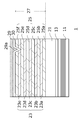
- FIG. 9 is a schematic drawing showing a cross-sectional structure of the semiconductor light emitting device of the present invention.
- the same components as those in FIGS. 5 and 7 are denoted by the same reference numerals.
- the dimensional ratio in the drawing does not necessarily match the actual dimensional ratio.
- the semiconductor light emitting device 1 has an undoped layer 13 and an n-type semiconductor layer 21 on the growth substrate 11.
- the semiconductor light emitting device 1 includes an active layer 27 in which barrier layers 25 and light emitting layers 23 are alternately stacked on an upper layer of an n-type semiconductor layer 21, and a protective layer 30 and a p-type semiconductor on the upper layer of the active layer 27. Layer 29 is provided.
- a barrier layer 25 (25a, 25b, 25c, 25d, 25e, 25f) made of an AlGaN layer with a thickness of 20 nm and a light emitting layer 23 (23a, 25f) made of an InGaN layer with a thickness of 10 nm. 23b, 23c, 23d, and 23e) were alternately laminated.
- the number of repetitions (period number) of the barrier layer 25 and the light emitting layer 23 can be set as appropriate.
- AlGaN is synonymous with the description of Al m Ga 1-m N (0 ⁇ m ⁇ 1), and the description of the composition ratio of Al and Ga is simply omitted. The intention is not limited to the case where the composition ratio of Al and Ga is 1: 1. The same applies to the description “InGaN”. In the following, it will be described in the same manner as described above.
- the growth substrate 11 is composed of a sapphire substrate.
- Si, SiC, GaN, YAG, or the like may be used.
- the undoped layer 13 is formed of GaN. More specifically, it is formed of a low-temperature buffer layer made of GaN and an underlying layer made of GaN on the upper layer.
- the n-type semiconductor layer 21 has a multilayer structure including, for example, a layer composed of AlGaN (electron supply layer) and a layer composed of GaN (protective layer). At least the protective layer is doped with an n-type impurity such as Si, Ge, S, Se, Sn, or Te.
- the protective layer 30 is composed of an AlGaN layer having a p-type impurity concentration lower than that of the p-type semiconductor layer 29.
- the protective layer 30 may have a p-type impurity concentration that is low enough to be recognized as an undoped layer.
- the protective layer 30 may be composed of an AlGaN layer doped with an n-type impurity such as Si.
- it is not limited to AlGaN, but may be composed of AlInGaN made of a quaternary mixed crystal, or may be composed of AlN or GaN.
- the p-type semiconductor layer 29 is made of, for example, GaN, AlGaN, or the like, and is doped with p-type impurities such as Mg, Be, Zn, or C. In particular, the p-type semiconductor layer 29 is doped with p-type impurities made of Mg. I do not care.
- the p-type semiconductor layer 29 has a protruding portion 29 a whose tip reaches the inside of the protective layer 30.
- the protruding portion 29a has a tip that remains at the height position of the final barrier layer 25f and does not reach at least the height position of the upper surface of the light emitting layer 23e.
- Step S1> an undoped layer 13 is formed on the growth substrate 11. For example, the following steps are performed.
- the c-plane sapphire substrate is cleaned. More specifically, for this cleaning, for example, a c-plane sapphire substrate is placed in a processing furnace of a MOCVD (Metal Organic Chemical Vapor Deposition) apparatus, and hydrogen gas with a flow rate of 10 slm is placed in the processing furnace. The temperature in the furnace is raised to, for example, 1150 ° C. while flowing.
- MOCVD Metal Organic Chemical Vapor Deposition
- a low-temperature buffer layer made of GaN is formed on the surface of the growth substrate 11 (c-plane sapphire substrate), and an underlayer made of GaN is further formed thereon. These low-temperature buffer layer and underlayer correspond to the undoped layer 13.
- a more specific method of forming the undoped layer 13 is as follows. First, the furnace pressure of the ⁇ CVD apparatus is 100 kPa, and the furnace temperature is 480 ° C. Then, nitrogen gas and hydrogen gas having a flow rate of 5 slm are supplied as carrier gases into the processing furnace, while TMG having a flow rate of 50 ⁇ mol / min and ammonia having a flow rate of 250,000 ⁇ mol / min are supplied to the processing furnace for 68 seconds. To do. Thereby, a low-temperature buffer layer made of GaN having a thickness of 20 nm is formed on the surface of the growth substrate 11.
- the furnace temperature of the MOCVD apparatus is raised to 1150 ° C. Then, while flowing nitrogen gas having a flow rate of 20 slm and hydrogen gas having a flow rate of 15 slm as a carrier gas in the processing furnace, TMG having a flow rate of 100 ⁇ mol / min and ammonia having a flow rate of 250,000 ⁇ mol / min are introduced into the processing furnace as source gases. Feed for 30 minutes. As a result, a base layer made of GaN having a thickness of 1.7 ⁇ m is formed on the surface of the low-temperature buffer layer.
- n-type semiconductor layer 21 made of n-type AlGaN is formed on the undoped layer 13.
- a specific forming method is as follows, for example.
- the furnace pressure of the MOCVD apparatus is set to 30 kPa. Then, while flowing nitrogen gas having a flow rate of 20 slm and hydrogen gas having a flow rate of 15 slm as a carrier gas into the processing furnace, TMG having a flow rate of 94 ⁇ mol / min, TMA having a flow rate of 6 ⁇ mol / min, and a flow rate of 250,000 ⁇ mol / min. Ammonia of min and tetraethylsilane having a flow rate of 0.025 ⁇ mol / min are supplied into the processing furnace for 60 minutes. Thereby, for example, an n-type semiconductor layer 21 having a composition of Al 0.06 Ga 0.94 N, a Si concentration of 3 ⁇ 10 19 / cm 3 , and a thickness of 2 ⁇ m is formed on the undoped layer 13.
- n-type GaN layer having a protective layer made of n-type GaN having a thickness of about 5 nm is formed on the n-type AlGaN layer.
- the semiconductor layer 21 may be realized.
- Si is used as the n-type impurity contained in the n-type semiconductor layer 21 .
- Ge, S, Se, Sn, Te, or the like can be used as the n-type impurity in addition to Si. .
- This step S2 corresponds to the step (a).
- an active layer 27 in which a light emitting layer made of InGaN and a barrier layer made of AlGaN are periodically repeated is formed on the n-type semiconductor layer 21.
- a specific forming method is as follows, for example.
- the furnace pressure of the MOCVD apparatus is 100 kPa, and the furnace temperature is 780 ° C. Then, while flowing nitrogen gas having a flow rate of 15 slm and hydrogen gas having a flow rate of 1 slm as a carrier gas in the processing furnace, TMG having a flow rate of 10 ⁇ mol / min, TMA having a flow rate of 1.6 ⁇ mol / min,.
- Step S3A is performed in which tetraethylsilane of 09 ⁇ mol / min and ammonia having a flow rate of 300000 ⁇ mol / min are supplied into the processing furnace for 480 seconds to form a barrier layer 25a made of an AlGaN layer having a thickness of 20 nm and an Al composition of 6%.
- step S3B is performed in which TMG having a flow rate of 10 ⁇ mol / min, TMI having a flow rate of 2 ⁇ mol / min, and ammonia having a flow rate of 300,000 ⁇ mol / min are supplied into the processing furnace for 240 seconds while the carrier gas is flowing.
- the light emitting layer 23a made of an InGaN layer having a thickness of 10 nm and an In composition of 1% is formed.
- steps S3A and S3B are alternately repeated, so that the barrier layer 25a, the light emitting layer 23a, the barrier layer 25b, the light emitting layer 23b, the barrier layer 25c, the light emitting layer 23c, the barrier layer 25d, the light emitting layer 23d, the barrier layer 25e, A stacked body of the light emitting layer 23e and the barrier layer 25f is formed. Thereby, the active layer 27 is formed.
- the barrier layer 25f corresponds to the final barrier layer.
- This step S3 corresponds to the step (b).
- the protective layer 30 is formed on the active layer 27.
- the undoped AlGaN layer is increased to, for example, about 4 nm.
- the protective layer 30 is formed by growing.
- the protective layer 30 is made of AlGaN having an Al composition of 6%.
- the film thickness is determined so that the tip of the pit 71 does not reach the height position of the upper surface of the light emitting layer 23e closest to the final barrier layer 25f.
- a schematic diagram of the cross-sectional structure of the element at this time is shown in FIG.
- the tip of the pit 71 remains at the position of the final barrier layer 25f, and the height of the upper surface of the lower light emitting layer 23e. The position has not been reached.
- the semiconductor layer can be grown in the lateral (horizontal) growth mode by growing the protective layer 30 at an extremely higher temperature than the step S3 (here, about 1025 ° C.). Therefore, a part of the pit 71 can be embedded by the protective layer 30 with a very thin film thickness of about 4 nm.
- the protective layer 30 is formed to be thinner than the barrier layers (25a, 25b, 25c, 25d, 25e, 25f).
- This step S4 corresponds to the step (c).
- a p-type semiconductor layer 29 made of, for example, AlGaN is formed on the protective layer 30.
- a specific forming method is as follows, for example.
- TMG with a flow rate of 35 ⁇ mol / min
- TMA with a flow rate of 20 ⁇ mol / min
- ammonia with a flow rate of 250,000 ⁇ mol / min
- biscyclopentadienyl magnesium with a flow rate of 0.1 ⁇ mol / min for doping p-type impurities (Cp 2 Mg) is supplied into the processing furnace for 60 seconds.
- a hole supply layer having a composition of Al 0.3 Ga 0.7 N having a thickness of 20 nm is formed on the protective layer 30.
- a hole supply layer having a composition of Al 0.13 Ga 0.87 N having a thickness of 120 nm is formed.
- a p-type semiconductor layer 29 is formed by these hole supply layers.
- the p-type impurity concentration of the p-type semiconductor layer 29 is, for example, about 3 ⁇ 10 19 / cm 3 .
- the supply of TMA is stopped, the flow rate of Cp 2 Mg is changed to 0.2 ⁇ mol / min, and the source gas is supplied for 20 seconds, whereby the thickness is about 5 nm and the p-type impurity concentration is 1 ⁇ .
- a p-type contact layer of about 10 20 / cm 3 may be formed.
- the p-type semiconductor layer 29 includes this p-type contact layer.
- This step S5 corresponds to the step (d).
- the p-type impurities contained in the p-type semiconductor layer 29 may diffuse to the protective layer 30 side when the wafer is exposed to a high temperature in the process of step S5.
- the protective layer 30 formed as an undoped layer in step S4 is formed as a layer containing a low-concentration p-type impurity when step S5 is completed.
- the protective layer 30 contains a p-type impurity diffused from the p-type semiconductor layer 29, the p-type impurity concentration is significantly lower than that of the p-type semiconductor layer 29.
- the p-type impurity concentration of the p-type semiconductor layer 29 is about 2 to 3 ⁇ 10 19 / cm 3
- the p-type impurity concentration of the protective layer 30 at the end of step S4 is 0.1 to 1 ⁇ It is about 10 19 / cm 3 .
- the p-type impurity when the p-type impurity is diffused from the p-type semiconductor layer 29 side and thus the protective layer 30 contains the p-type impurity, the side closer to the p-type semiconductor layer 29 in the protective layer 30 is the p-type impurity. It is considered that the p-type impurity concentration decreases as the impurity concentration increases and the distance from the p-type semiconductor layer 29 increases. Therefore, the p-type impurity concentration in the region near the final barrier layer 25f in the protective layer 30 is significantly lower than the p-type impurity concentration in the p-type semiconductor layer 29, and may still show a value that is about the detection limit. .
- the tip of the pit 71 remains at the height position of the final barrier layer 25f, and reaches the height position of the upper surface of the lower light emitting layer 23e. Therefore, even if a p-type impurity is introduced thereafter, the situation where the p-type impurity diffuses into the light emitting layer 23e is suppressed. As a result, the tip of the protrusion 29a formed by the diffusion of the p-type impurity in the pit 71 does not reach the light emitting layer 23e (see FIG. 9).
- Step S6 an activation process is performed on the wafer obtained through steps S1 to S5. More specifically, activation is performed at 650 ° C. for 15 minutes in a nitrogen atmosphere using an RTA (Rapid Thermal Anneal) device.
- RTA Rapid Thermal Anneal
- an electrode is formed at a location where the growth substrate 11 was present to form an n-side electrode.
- etching is performed from the p side until the n type semiconductor layer is exposed to form an n side electrode.
- an electrode such as a transparent electrode may be formed as necessary.
- a power supply terminal or the like is formed on each electrode, and if necessary, the exposed element side surface or upper surface is covered with a highly light-transmitting insulating layer and connected to the substrate by wire bonding or the like.
- Example 1 The semiconductor light emitting device 1 manufactured as a horizontal LED device through the above steps S1 to S6 was taken as Example 1. At this time, in step S4, the temperature when forming the protective layer 30 was set to 1025 ° C., and the film thickness of the protective layer 30 was set to 4 nm.
- step S4 the protective layer 30 is made of AlGaN having an Al composition of 10%, the temperature when forming the protective layer 30 is set to 780 ° C. lower than that in Example 1, and the film thickness of the protective layer 30 is set to 20 nm. Except for this point, Example 2 was a semiconductor light-emitting device 1 manufactured by the same method as Example 1. Since the growth temperature of the protective layer 30 is lower than that in the first embodiment, the lateral (horizontal) growth mode does not appear so much. In order not to reach the position, the protective layer 30 is formed with a thicker film than in the first embodiment.
- Comparative Example 1 The semiconductor light emitting device manufactured as a horizontal LED device through steps S1 to S3 and steps S5 to S6 was used as the device of Comparative Example 1. That is, Comparative Example 1 is different from Examples 1 and 2 in that the protective layer 30 is not provided.
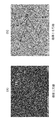
- FIG. 11 is a photograph of the layer surface in the state immediately before the growth of the p-type semiconductor layer 29 in Example 1, Example 2, and Comparative Example 1, and was taken with an AFM (Atomic Force Microscopy). It has been done.
- AFM Acoustic Force Microscopy
- the darkest spots are conspicuous in the element of Comparative Example 1, which indicates that many pits 71 having a large diameter appear.
- the pit 71 is slightly less noticeable than the device of Comparative Example 1, but this is because the pit 71 is partially embedded by the protective layer 30 formed of a thick film. The reason is that the diameter is smaller than that of the element of Comparative Example 1.
- the presence of the pits 71 is less noticeable than in the second embodiment. This is because the growth temperature of the protective layer 30 in Example 1 was higher than that in Example 2, so that the protective layer 30 grew in the lateral mode, and the diameter of the pits 71 was significantly reduced. Moreover, it is considered that some of the pits 71 that have appeared are completely filled with the protective layer 30.
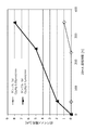
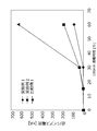
- FIG. 12 is a graph showing Ir characteristics when reverse bias is applied to the elements of Example 1, Example 2, and Comparative Example 1, respectively. Specifically, a reverse bias current that flows when a reverse bias of ⁇ 5 V was applied after supplying (aging) a current of 100 mA to each element for a predetermined time was measured.
- the horizontal axis represents the time during which current is supplied for aging (aging time), and the vertical axis represents the reverse bias current that flows through the element when a reverse bias voltage is applied.
- the reverse bias current of the element of Comparative Example 1 increases rapidly.
- the reverse bias current of the element of Example 2 is suppressed more than that of the element of Comparative Example 1, and the reverse bias current of the element of Example 1 is further suppressed than that of the element of Example 2.
- the p-type impurity diffuses into the light emitting layer (23e, etc.) through the pits 71, so that the pn junction is destroyed and a leak current is generated, which is high. It is thought that it appears as a reverse bias current.
- the formation of the protective layer 30 causes p-type impurities to diffuse into the light emitting layer 23e as a result of filling a part of the pits 71. It is suppressed, and it is considered that the leakage current can be reduced as compared with the element of Comparative Example 1.
- the protective layer 30 was grown at a high temperature, so that a part of the pits 71 could be effectively filled with the protective layer 30 which is thinner than the element of Example 2. It is inferred.
- the tip of the protruding portion 29 a of the p-type semiconductor layer 29 may be configured not to reach the height position of the upper surface of the final barrier layer 25 f.
Landscapes
- Led Devices (AREA)
Abstract
リーク電流の発生を抑止して発光効率を高めた半導体発光素子を実現する。 n型半導体層とp型半導体層の間に、発光層及び障壁層が交互に積層されてなる活性層を有する半導体発光素子であって、障壁層のうちp型半導体層に最も近接する側に形成された最終障壁層の上面に、最終障壁層とは異なる層であって、p型半導体層よりはp型不純物濃度が低い保護層を有し、保護層の上面にp型半導体層が形成されている。
Description
本発明は、n型半導体層とp型半導体層の間に、発光層及び障壁層が交互に積層されてなる活性層を有する半導体発光素子、及びその製造方法に関する。
紫外光を発する半導体発光素子には、露光、キュア、殺菌、医療、センサ用途といった幅広い応用製品があり、今後大きな市場が期待される。
紫外光を発する半導体発光素子としてInGaN系のものが知られている。従来のInGaN系の半導体発光素子は、サファイア等からなる成長基板上に、n型半導体層と、障壁層及び発光層が交互に積層されてなる活性層と、p型半導体層とを積層してなる半導体層を成長させ、基板上に塗布したハンダを利用して成長基板上の半導体層と支持基板とを貼り合わせた後、レーザリフトオフにより成長基板を剥離して作成されるものが主流である。
現在普及しているInGaN系の半導体発光素子の大部分は、サファイア基板上に、GaN層及びInGaN層をエピタキシャル成長させることにより形成される。このとき、サファイアと、GaN及びInGaNでは格子定数が異なるため、成長層内に高密度の転位と呼ばれる結晶欠陥が存在することが知られている(例えば特許文献1、2参照)。
N. Kuroda, C. Sasaoka, A. Kimura, A. Usui and Y. Mochizuki,"Precise control of pn-junction profile for GaN-based LD structures using GaN substrates with low dislocation densities", J. Cryst. Growth 189/190 (1998) 551
成長基板として、サファイア基板に代えて低転位GaN基板を用いた場合、その上のエピタキシャル層も基板と同様に低転位密度とすることは可能である。しかし、レーザリフトオフに使用されるレーザ光の波長は300nm以下のものが主流であるところ、このレーザ光はGaN基板を透過しないため、GaN基板を剥離することが困難である。このように、GaN基板を成長基板として使用する方法では、高出力の紫外光発光素子を作成することが困難であるため、成長基板としてサファイア基板を用いることが主流となっている。
しかし、上述したように、InGaN系の半導体発光素子は、格子定数の異なるサファイア基板上に、GaN層及びInGaN層をエピタキシャル成長しているため、転位と呼ばれる結晶欠陥が存在する。本発明者は、鋭意研究により、この転位に起因してリークが発生し、半導体発光素子の素子特性(例えばIr特性)を低下させていることを突き止めた。
図1は、従来方法で製造したInGaN系の半導体発光素子60に対し、p側パッド電極61とn側パッド電極62の間に微小電流を流したときの発光の様子を示す写真である。初期時においては発光箇所が見受けられないが、供給電流量を徐々に増加させていくと、青白く発光する箇所63が散見されるようになる。特に、p側パッド電極61の周辺において発光箇所63が多く現れている。
図2は、一の発光箇所63における半導体発光素子60の断面をTEM(Transmission Electron Microscope:透過型電子顕微鏡)にて撮影した写真である。(b)は(a)を拡大したものである。
図2によれば、発光箇所63の位置において、半導体発光素子60に転位65が生じていることが確認される。図2(b)は、活性層67とp型半導体層68が形成されている箇所を拡大したものであり、この箇所に転位65が生じていることが分かる。本発明者は、従来方法によって製造された半導体発光素子60のIr特性が低下している原因は、この転位65を原因としたリークの発生によるものではないかと推察した。より詳細には、転位65に起因して何らかのピット(凹部)が形成され、このピットを介してp型半導体層68に含まれるp型不純物であるMgが活性層67やn型半導体層へと拡散することで、pn接合が破壊されてリークが生じ、図1の写真のような発光箇所63が形成されたものと推察した。
図3は、転位密度の異なる2つのInGaN系の半導体発光素子に対して、SIMS(Secondary Ion Mass Spectrometry:二次イオン質量分析法)によって深さ方向にMg濃度を測定したグラフである(上記非特許文献1参照)。図3において、(a)が、転位密度が1×10⁹/cm2オーダーの素子の結果を示すグラフであり、(b)が、転位密度が6×107/cm2の素子の結果を示すグラフである。
図3によれば、(a)の結果においてp型半導体層68に起因するMgの信号が、深さ1μm~2.5μm付近で現れており、これは活性層67内にMgが侵入していることを示唆している。これに対し、(b)の結果では活性層67の位置においてMgは検出限界値(バックグラウンドレベル)に留まっており、活性層67内にはMgが侵入していないことが分かる。つまり、転位密度が高い素子においては、p型半導体層68側から活性層67内にMgが拡散していることが分かる。
図4は、従来と同様の構成を有するInGaN系半導体発光素子60において、活性層67を形成した直後における表面状態を撮影したSEM写真である。また、図5は、図4の状態の素子の断面構造を示す模式的な図面である。この発光素子60は、成長基板11としてサファイア基板を用い、成長基板11上にアンドープ層13及びn型半導体層21を成長させた後、膜厚20nmのAlGaN層からなる障壁層25(25a,25b,25c,25d,25e,25f)と、膜厚10nmのInGaN層からなる発光層23(23a,23b,23c,23d,23e)を交互に積層してなる構成である。なお、障壁層25fが最終障壁層に対応する。
より詳細には、炉内温度を820℃とし、所定のキャリアガス及びアンモニアを供給した状態で、トリメチルアルミニウム(TMA)の流量を1.6μmol/min、トリメチルガリウム(TMG)の流量を10μmol/minとして障壁層25を形成し、同様に所定のキャリアガス及びアンモニアを供給した状態で、トリメチルインジウム(TMI)の流量を2μmol/min、TMGの流量を10μmol/minとして発光層23を形成するステップを交互に行った。そして、最終障壁層25fを形成した後、p型半導体層を形成することなく、温度を室温まで低下させた状態で表面状態を撮影した写真が図4である。
図4によれば、最終障壁層25fの表面には複数のピット(凹部)71が形成されていることが確認される。特に(b)の写真からピット71の径(直径)は概ね70~90nmと推察され、GaN系において安定的に結晶の出やすい方位面の傾斜角度が約60°であることから鑑みれば、ピット71の径と深さはほぼ等しいと推察される。各発光層23の膜厚を10nmとし、各障壁層25の膜厚を20nmとしたことに鑑みれば、ピット71は最終障壁層25fの下層に位置する発光層23e、障壁層25e、発光層23d、及び障壁層25d程度まで達していると推察される。図5では、このようなピット71の状態を模式的に表示している。
図6は、従来と同様のInGaN系の半導体発光素子に関し、820℃の温度下で活性層67を形成した後、2分間でp型半導体層68を成長させる温度である1025℃まで昇温させた後、p型半導体層68を成長させることなく室温まで温度を低下させたときの表面状態を撮影したSEM写真である。図6は、図4と同様に、(a)が倍率1万倍の写真を示し、(b)が倍率10万倍の写真を示している。また、図7は、図6の状態の素子の断面構造を示す模式的な図面である。
図6(b)によれば、ピット71の径(直径)は概ね20~40nmと推察され、図4の状態よりもピット71の径が小さくなっていることが分かる。これは、温度が高くなることで、エピタキシャル成長のモードが、垂直方向に成長するモードから水平方向に成長するモード、すなわちピット71を埋め込むモードに変化した結果、ピット71の一部が埋められ、径及び深さが小さくなったものと推察される。より詳細には、温度を上げている間、熱平衡を保っている層表面の原料がエッチングされて動き、当該エッチングされた材料や炉内のガスがピット71内に入って水平方向に成長したことで、ピット71の一部(図7における領域71a)が埋められたものと考えられる。
上述の推察に従い、ピット71の深さが径とほぼ等しいとすると、図6におけるピット71の深さは約20~40nmと推察されるため、ピット71は、最終障壁層25fの下層に位置する発光層23eに達しており、一部のピット71は障壁層25eにも達していると考えられる。
つまり、この状態でp型半導体層68を形成すると、p型半導体層68に含まれるp型不純物が、ピット71を介して発光層23eに達し、一部のp型不純物は更に発光層23eの下層の障壁層25eにも達すると考えられる。本発明者は、以上の検討の下、かかるピット71の存在によってp型不純物が活性層67内に侵入し、pn接合が破壊されたことで、図1の写真に示すようなリーク電流が発生していることを突き止めた。
本発明は、上記の検討に鑑み、リーク電流の発生を抑止して発光効率を高めた半導体発光素子を実現することを目的とする。
本発明は、n型半導体層とp型半導体層の間に、発光層及び障壁層が交互に積層されてなる活性層を有する半導体発光素子であって、
前記障壁層のうち前記p型半導体層に最も近接する側に形成された最終障壁層の上面に、前記最終障壁層とは異なる層であって、前記p型半導体層よりはp型不純物濃度が低い保護層を有し、
前記保護層の上面に前記p型半導体層が形成されていることを特徴とする。
前記障壁層のうち前記p型半導体層に最も近接する側に形成された最終障壁層の上面に、前記最終障壁層とは異なる層であって、前記p型半導体層よりはp型不純物濃度が低い保護層を有し、
前記保護層の上面に前記p型半導体層が形成されていることを特徴とする。
上述した本発明者の鋭意研究により、従来の製造方法によれば、p型半導体層を形成する直前において活性層を構成する発光層内にピット(凹部)が達しており、このピットを通じてp型不純物が発光層内に侵入した結果、リーク電流が発生したものと考えられる。上記のような構成とすることで、製造時に形成されるピットの先端を保護層の高さ位置又は最終障壁層の高さ位置に留まらせ、その下層に位置する発光層には達しない状態を実現することができる。また、仮に一部のピットの先端が発光層の上面の高さ位置まで達していたとしても、従来と比べてその頻度を大幅に低下させることができる。これにより、従来よりもリーク電流を抑制することができる。この結果は、実施例を参照して後述される。
なお、この保護層は、製造時においてアンドープの層として形成された後、この保護層の上面にp型半導体層が形成される過程で高温下(例えば1000℃程度)に晒されることで、このp型半導体層からp型不純物が拡散されて、低濃度のp型不純物を含む層として形成されたものとしても構わない。このとき、保護層に含まれるp型不純物濃度が、厚さ方向に分布を有するものとしても構わない。
また、この保護層は、製造時において低濃度のn型不純物が含有された層、若しくは極めて低濃度のp型不純物が含有された層として形成された層であるものとしても構わない。
p型半導体層に含有されるp型不純物の濃度は、例えば1×10¹⁹/cm3よりは高濃度であり、好ましくは2~3×1019/cm3程度である。このとき、保護層に含有されるp型不純物濃度は、1×1019/cm3以下とすることができ、好ましくは1×1018/cm3以下である。
より詳細には、前記p型半導体層が、前記保護層の内部に侵入し、且つ先端が前記最終障壁層よりも前記n型半導体層側に形成された前記発光層の上面の高さ位置には達していない突出部を有する構成とすることができる。
最終障壁層の上面に保護層を形成したことにより、最終障壁層が形成された時点において当該最終障壁層の表面にピットが現れていた場合であっても、当該ピットの内部の少なくとも一部を保護層によって充填することが可能となる。特に、発光層にまで達していたピットの先端を保護層で充填することで、保護層を形成した後の時点においてピットの先端が発光層の上面の高さ位置に達しない状態が実現される。このような状態の下でp型半導体層を形成することで、仮にp型半導体層の形成開始時点においてピットが存在していても、このピットは発光層の上面の高さ位置には達していないため、p型半導体層にドープされているp型不純物が発光層に拡散することを抑制できる。
なお、ここでいう突出部は、p型半導体層を形成する直前において保護層内に残存形成されたピット(凹部)に、p型半導体層に含まれるp型不純物が拡散したことで形成されたものとして構わない。突出部の先端が発光層の上面の高さ位置に達していないことで、p型不純物が活性層内に拡散してpn接合が破壊される事態が回避される。
保護層としては、当該保護層の形成前時点で形成されているピットの先端部を充填することで、保護層を形成した後の時点において残存しているピットの先端が発光層の上面の高さ位置に達しない状態を実現するために必要な最低膜厚以上であれば良い。
また、前記保護層は、前記最終障壁層よりも薄膜で構成するものとしても構わない。保護層の厚みを厚くすると、p型不純物層と発光層の間の距離が遠くなるため、p型半導体層から供給された正孔が発光層に届きにくくなる。このとき、最終障壁層とp型半導体層の界面で電子が閉じ込められてしまい、不純物準位を形成して所望波長とは異なる波長の光を発光する場合がある。このような事態は、発光スペクトルを取得したときに、所望の波長とは別の箇所において少し大きな出力が見受けられる(いわゆるショルダー部分を有する。)ことから確認できる。このような事態が生じると、所望の波長の光に関する取り出し効率が低下してしまう。
よって、保護層としては、前記最低膜厚以上であって、可能な限り薄膜であることが好ましい。なお、このとき、保護層を横方向成長(水平方向成長)が可能な温度条件で成長させることで、膜厚をできる限り薄くしながらもピットの先端部分を埋め込むことができる。この温度条件は、最終障壁層を含む活性層の成長温度よりも高温であり、例えば1000℃以上とすることができる。
なお、前記p型半導体層は、p型不純物としてMgを含むものとしても構わない。
図8は、従来方法で製造したInGaN系半導体発光素子に対し、最終障壁層25fの上層に形成されるp型半導体層68の形成条件を変えたときの逆バイアス印加時におけるIr(逆方向電流)特性を示すグラフである。より詳細には、p型不純物をドープするための原料ガスであるビスシクロペンタジエニルマグネシウム(Cp2Mg)の流量を0.05μmol/minとして形成したサンプル(a)と、0.1μmol/minとして形成したサンプル(b)に対し、-5Vの逆バイアスを印加して20mA通電試験を行ったときの、通電時間とIrの関係を測定した。
これによれば、サンプル(a)と比較して、Mg供給量が多いサンプル(b)の方が、通電時間の経過と共にIrの値が高くなっていることが分かる。これにより、(a)と比較して(b)の方がリーク電流を発生しやすいサンプルであることが分かる。従って、p型半導体に含まれるp型不純物がMgの場合に、ピットを介して活性層内にp型不純物が侵入してリーク電流を引き起こすという上記の課題が顕著に現れるといえる。
よって、p型半導体層にドープされているp型不純物がMgである構成において、上記のように保護層を備えた半導体発光素子とすることで、リーク電流の抑制効果が大きく発揮される。
また、本発明の半導体発光素子の製造方法は、
基板上にn型半導体層を形成する工程(a)と、
前記n型半導体層上に発光層及び障壁層を交互に積層して活性層を形成する工程(b)と、
前記障壁層のうち前記p型半導体層に最も近接する側に形成された最終障壁層の上面に、前記最終障壁層とは異なる保護層を形成する工程(c)と、
p型のドーパントを供給して前記保護層の上面にp型半導体層を形成する工程(d)とを有し、
前記工程(c)において、当該工程(c)の開始前に層の最上面に出現しているピットの先端が少なくとも前記発光層の高さ位置には達しないように、当該ピットの少なくとも一部が前記保護層で充填されることを特徴とする。
基板上にn型半導体層を形成する工程(a)と、
前記n型半導体層上に発光層及び障壁層を交互に積層して活性層を形成する工程(b)と、
前記障壁層のうち前記p型半導体層に最も近接する側に形成された最終障壁層の上面に、前記最終障壁層とは異なる保護層を形成する工程(c)と、
p型のドーパントを供給して前記保護層の上面にp型半導体層を形成する工程(d)とを有し、
前記工程(c)において、当該工程(c)の開始前に層の最上面に出現しているピットの先端が少なくとも前記発光層の高さ位置には達しないように、当該ピットの少なくとも一部が前記保護層で充填されることを特徴とする。
上記方法によれば、p型半導体層を成長させる工程(d)の開始前の時点において、層に形成されているピットの先端を保護層又は最終障壁層内に留まらせ、その下層に形成されている発光層の高さ位置には達しない状態が実現される。この状態でp型半導体層を形成することで、p型不純物はピットを通じて保護層又は最終障壁層までは拡散するものの、その下層の発光層までは拡散しない。これによりpn接合が破壊されず、リーク電流の発生が抑制される。
ここで、前記工程(c)を、横方向成長が可能な温度条件で所定の半導体層を成長させることで前記保護層を形成する工程とすることができる。この温度条件は、最終障壁層を含む活性層の成長温度よりも高温であり、例えば1000℃以上とすることができる。このような製法とすることで、保護層の厚みを出来る限り薄くしながらも、工程(d)の開始前時点において、ピットの先端を保護層又は最終障壁層内に留まらせることが可能となる。
更にこのとき、前記工程(c)を、前記最終障壁層より薄膜で前記保護層を成長させる工程としても構わない。
また、前記工程(d)において、前記p型のドーパントを、Mgを含む材料としても構わない。
なお、前記工程(c)は、アンドープの半導体層を成長させることで前記保護層を形成する工程であるものとしても構わない。
本発明によれば、リーク電流の発生を抑止して発光効率を高めた半導体発光素子が実現される。
以下において、本発明の半導体発光素子及びその製造方法の実施形態について説明する。まず、半導体発光素子の構造及び製造方法の一例について説明をした後、実施例を参照して特性を評価する。
[構造]
図9は、本発明の半導体発光素子の断面構造を示す模式的な図面であり、図5及び図7と同一の構成要素については、同一の符号を付している。なお、各図において図面の寸法比と実際の寸法比は必ずしも一致しない。
図9は、本発明の半導体発光素子の断面構造を示す模式的な図面であり、図5及び図7と同一の構成要素については、同一の符号を付している。なお、各図において図面の寸法比と実際の寸法比は必ずしも一致しない。
半導体発光素子1は、成長基板11の上層に、アンドープ層13と、n型半導体層21を有する。半導体発光素子1は、n型半導体層21の上層には、障壁層25と発光層23が交互に積層されてなる活性層27を備え、活性層27の上層には保護層30及びp型半導体層29を備える。
本実施形態では、活性層27として、膜厚20nmのAlGaN層からなる障壁層25(25a,25b,25c,25d,25e,25f)と、膜厚10nmのInGaN層からなる発光層23(23a,23b,23c,23d,23e)を交互に積層した。なお、障壁層25及び発光層23の繰り返し回数(周期数)は、適宜設定することができる。
なお、「AlGaN」という記述は、AlmGa1-mN(0<m<1)という記述と同義であり、AlとGaの組成比の記述を単に省略して記載したものであって、AlとGaの組成比が1:1である場合に限定する趣旨ではない。「InGaN」という記述についても同様である。以下においても上記にならって記載される。
成長基板11は、サファイア基板で構成される。なお、サファイアの他、Si、SiC、GaN、YAGなどで構成しても構わない。
アンドープ層13は、GaNにて形成される。より具体的には、GaNよりなる低温バッファ層と、その上層にGaNよりなる下地層によって形成される。
n型半導体層21は、例えばAlGaNで構成される層(電子供給層)とGaNで構成される層(保護層)を含む多層構造で構成される。少なくとも保護層には、Si、Ge、S、Se、Sn、又はTe等のn型不純物がドープされている。
本実施形態において、保護層30はp型半導体層29よりもp型不純物濃度が低いAlGaN層で構成されている。例えば、保護層30は、実質的にアンドープ層と認められる程度にp型不純物濃度が低いものとしても構わない。また、保護層30をSi等のn型不純物がドープされたAlGaN層で構成しても構わない。また、AlGaNに限らず、四元混晶からなるAlInGaNで構成しても構わないし、AlNやGaNで構成しても構わない。
p型半導体層29は、例えばGaN、AlGaN等で構成され、Mg、Be、Zn、又はC等のp型不純物がドープされているが、特にMgからなるp型不純物がドープされているものとして構わない。
図9に示すように、p型半導体層29は、先端が保護層30内に達する突出部29aを有する。この突出部29aは、本実施形態では、その先端が最終障壁層25fの高さ位置に留まっており、少なくとも発光層23eの上面の高さ位置には達していない。
[製造方法]
次に、半導体発光素子1の製造方法の一例につき、説明する。なお、下記製造方法で説明する製造条件や膜厚などの寸法は、あくまで一例であって、これらの数値に限定されるものではない。
次に、半導体発光素子1の製造方法の一例につき、説明する。なお、下記製造方法で説明する製造条件や膜厚などの寸法は、あくまで一例であって、これらの数値に限定されるものではない。
<ステップS1>
まず、成長基板11上に、アンドープ層13を形成する。例えば、以下の工程により行われる。
まず、成長基板11上に、アンドープ層13を形成する。例えば、以下の工程により行われる。
(成長基板11の準備)
成長基板11としてサファイア基板を用いる場合、c面サファイア基板のクリーニングを行う。このクリーニングは、より具体的には、例えばMOCVD(Metal Organic Chemical Vapor Deposition:有機金属化学気相蒸着)装置の処理炉内にc面サファイア基板を配置し、処理炉内に流量が10slmの水素ガスを流しながら、炉内温度を例えば1150℃に昇温することにより行われる。
成長基板11としてサファイア基板を用いる場合、c面サファイア基板のクリーニングを行う。このクリーニングは、より具体的には、例えばMOCVD(Metal Organic Chemical Vapor Deposition:有機金属化学気相蒸着)装置の処理炉内にc面サファイア基板を配置し、処理炉内に流量が10slmの水素ガスを流しながら、炉内温度を例えば1150℃に昇温することにより行われる。
(アンドープ層13の形成)
次に、成長基板11(c面サファイア基板)の表面に、GaNよりなる低温バッファ層を形成し、更にその上層にGaNよりなる下地層を形成する。これら低温バッファ層及び下地層がアンドープ層13に対応する。
次に、成長基板11(c面サファイア基板)の表面に、GaNよりなる低温バッファ層を形成し、更にその上層にGaNよりなる下地層を形成する。これら低温バッファ層及び下地層がアンドープ層13に対応する。
アンドープ層13のより具体的な形成方法は例えば以下の通りである。まず、МОCVD装置の炉内圧力を100kPa、炉内温度を480℃とする。そして、処理炉内にキャリアガスとして流量がそれぞれ5slmの窒素ガス及び水素ガスを流しながら、原料ガスとして、流量が50μmol/minのTMG及び流量が250000μmol/minのアンモニアを処理炉内に68秒間供給する。これにより、成長基板11の表面に、厚みが20nmのGaNよりなる低温バッファ層を形成する。
次に、MOCVD装置の炉内温度を1150℃に昇温する。そして、処理炉内にキャリアガスとして流量が20slmの窒素ガス及び流量が15slmの水素ガスを流しながら、原料ガスとして、流量が100μmol/minのTMG及び流量が250000μmol/minのアンモニアを処理炉内に30分間供給する。これにより、低温バッファ層の表面に、厚みが1.7μmのGaNよりなる下地層を形成する。
<ステップS2>
次に、アンドープ層13の上層に、n型AlGaNで構成されるn型半導体層21を形成する。具体的な形成方法は例えば以下の通りである。
次に、アンドープ層13の上層に、n型AlGaNで構成されるn型半導体層21を形成する。具体的な形成方法は例えば以下の通りである。
まず、引き続き炉内温度を1150℃とした状態で、MOCVD装置の炉内圧力を30kPaとする。そして、処理炉内にキャリアガスとして流量が20slmの窒素ガス及び流量が15slmの水素ガスを流しながら、原料ガスとして、流量が94μmol/minのTMG、流量が6μmol/minのTMA、流量が250000μmol/minのアンモニア及び流量が0.025μmol/minのテトラエチルシランを処理炉内に60分間供給する。これにより、例えばAl0.06Ga0.94Nの組成を有し、Si濃度が3×1019/cm3で、厚みが2μmのn型半導体層21がアンドープ層13の上層に形成される。
なお、この後、TMAの供給を停止すると共に、それ以外の原料ガスを6秒間供給することにより、n型AlGaN層の上層に、厚みが5nm程度のn型GaNよりなる保護層を有するn型半導体層21を実現してもよい。
上記の説明では、n型半導体層21に含まれるn型不純物をSiとする場合について説明したが、n型不純物としては、Si以外にGe、S、Se、Sn又はTe等を用いることができる。
このステップS2が工程(a)に対応する。
<ステップS3>
次に、n型半導体層21の上層にInGaNで構成される発光層及びAlGaNで構成される障壁層が周期的に繰り返される活性層27を形成する。具体的な形成方法は例えば以下の通りである。
次に、n型半導体層21の上層にInGaNで構成される発光層及びAlGaNで構成される障壁層が周期的に繰り返される活性層27を形成する。具体的な形成方法は例えば以下の通りである。
まずMOCVD装置の炉内圧力を100kPa、炉内温度を780℃とする。そして、処理炉内にキャリアガスとして流量が15slmの窒素ガス及び流量が1slmの水素ガスを流しながら、原料ガスとして、流量が10μmol/minのTMG、流量が1.6μmol/minのTMA、0.09μmol/minのテトラエチルシラン及び流量が300000μmol/minのアンモニアを処理炉内に480秒間供給するステップS3Aを行って、膜厚20nm、Al組成6%のAlGaN層からなる障壁層25aを形成する。
次に、前記キャリアガスを流しながら、原料ガスとして、流量が10μmol/minのTMG、流量が2μmol/minのTMI及び流量が300000μmol/minのアンモニアを処理炉内に240秒間供給するステップS3Bを行って、膜厚10nm、In組成1%のInGaN層からなる発光層23aを形成する。
以下、前記ステップS3A及びS3Bを交互に繰り返すことで、障壁層25a、発光層23a、障壁層25b、発光層23b、障壁層25c、発光層23c、障壁層25d、発光層23d、障壁層25e、発光層23e、及び障壁層25fの積層体を形成する。これにより、活性層27が形成される。なお、本実施形態の構成では、障壁層25fが最終障壁層に対応する。
このステップS3が工程(b)に対応する。
<ステップS4>
次に、活性層27の上層に、保護層30を形成する。具体的な一例としては、次のステップS5においてp型半導体層29を形成する際の炉内温度とほぼ同等の温度(例えば1025℃)程度まで上昇させた後、アンドープのAlGaN層を例えば4nm程度成長させることで保護層30を形成する。なお、ここでは保護層30をAl組成6%のAlGaNで構成した。
次に、活性層27の上層に、保護層30を形成する。具体的な一例としては、次のステップS5においてp型半導体層29を形成する際の炉内温度とほぼ同等の温度(例えば1025℃)程度まで上昇させた後、アンドープのAlGaN層を例えば4nm程度成長させることで保護層30を形成する。なお、ここでは保護層30をAl組成6%のAlGaNで構成した。
ここで、保護層30を形成するにあたっては、ピット71の先端が、最終障壁層25fに最も近い発光層23eの上面の高さ位置に達しないように膜厚を決定する。この時点における素子の断面構造の模式図を図7にならって図10に示す。図10に示すように、ピット71の一部が保護層30で充填された結果、当該ピット71の先端が最終障壁層25fの位置に留まっており、その下層の発光層23eの上面の高さ位置には達していない。
ステップS3よりも極めて高温(ここでは1025℃程度)で保護層30を成長させることで、横方向(水平方向)の成長モードで半導体層を成長させることができる。このため、4nm程度といった極めて薄い膜厚で保護層30によってピット71の一部を埋め込むことが可能となる。なお、本実施形態において、保護層30の膜厚は、障壁層(25a,25b,25c,25d,25e,25f)の膜厚よりも薄膜で形成されている。
このステップS4が工程(c)に対応する。
<ステップS5>
次に、保護層30の上層に、例えばAlGaNで構成されるp型半導体層29を形成する。具体的な形成方法は例えば以下の通りである。
次に、保護層30の上層に、例えばAlGaNで構成されるp型半導体層29を形成する。具体的な形成方法は例えば以下の通りである。
原料ガスとして、流量が35μmol/minのTMG、流量が20μmol/minのTMA、流量が250000μmol/minのアンモニア及びp型不純物をドープするための流量が0.1μmol/minのビスシクロペンタジエニルマグネシウム(Cp2Mg)を処理炉内に60秒間供給する。これにより、保護層30の上層に、厚みが20nmのAl0.3Ga0.7Nの組成を有する正孔供給層を形成する。その後、TMAの流量を4μmol/minに変更して原料ガスを360秒間供給することにより、厚みが120nmのAl0.13Ga0.87Nの組成を有する正孔供給層を形成する。これらの正孔供給層によりp型半導体層29が形成される。このp型半導体層29のp型不純物濃度は、例えば3×1019/cm3程度である。
なお、その後、TMAの供給を停止すると共に、Cp2Mgの流量を0.2μmol/minに変更して原料ガスを20秒間供給することにより、厚みが5nm程度で、p型不純物濃度が1×1020/cm3程度のp型コンタクト層を形成してもよい。この場合、p型半導体層29にはこのp型コンタクト層も含まれる。
このステップS5が工程(d)に対応する。なお、このステップS5の過程でウェハが高温下に晒されることで、p型半導体層29に含まれるp型不純物が保護層30側に拡散する場合がある。このとき、ステップS4においてアンドープ層で形成されていた保護層30は、ステップS5が終了した時点において、低濃度のp型不純物を含有した層として形成される。ただし、保護層30が、p型半導体層29から拡散したp型不純物を含有したとしても、p型不純物濃度は、p型半導体層29と比べて著しく低い。例えば、p型半導体層29のp型不純物濃度が2~3×10¹⁹/cm3程度である場合において、ステップS4の終了時点における保護層30のp型不純物濃度は、0.1~1×1019/cm3程度である。
しかも、p型半導体層29側からp型不純物が拡散されたことで保護層30にp型不純物が含まれる場合、保護層30内においては、p型半導体層29に近い側の方がp型不純物濃度が高く、p型半導体層29から離れるほどp型不純物濃度が低くなると考えられる。従って、保護層30内のうち、最終障壁層25fに近い領域のp型不純物濃度は、p型半導体層29のp型不純物濃度に比べて著しく低く、依然として検出限界程度の値を示す場合もある。
図10に示すように、p型不純物を導入する直前の状態において、ピット71の先端が最終障壁層25fの高さ位置に留まっており、その下層の発光層23eの上面の高さ位置に達していないため、その後にp型不純物を導入しても、当該p型不純物が発光層23eに拡散する事態が抑制される。この結果、ピット71内にp型不純物が拡散することで形成される突出部29aの先端は発光層23eには達しない(図9参照)。
<ステップS6>
次に、ステップS1~S5を経て得られたウェハに対して活性化処理を行う。より具体的には、RTA(Rapid Thermal Anneal:急速加熱)装置を用いて、窒素雰囲気下中650℃で15分間の活性化処理を行う。
次に、ステップS1~S5を経て得られたウェハに対して活性化処理を行う。より具体的には、RTA(Rapid Thermal Anneal:急速加熱)装置を用いて、窒素雰囲気下中650℃で15分間の活性化処理を行う。
その後は、縦型のLED素子を実現する場合には、成長基板11を剥離した後、当該成長基板11が存在していた箇所に電極を形成してn側電極を形成する。また、横型のLED素子を実現する場合には、p側からn型半導体層が露出するまでエッチングを行なって、n側電極を形成する。なお、この場合、必要に応じて透明電極などの電極を形成するものとしても構わない。その後、各電極に給電端子などを形成し、必要に応じて、露出されている素子側面や上面を透光性の高い絶縁層で覆い、ワイヤボンディングなどにより基板との接続を行う。
以下、実施例及び比較例を参照して説明する。
(実施例1)
上記ステップS1~S6を経て、横型のLED素子として製造された半導体発光素子1を実施例1とした。なお、このときステップS4において、保護層30を形成する際の温度を1025℃とし、保護層30の膜厚を4nmとした。
上記ステップS1~S6を経て、横型のLED素子として製造された半導体発光素子1を実施例1とした。なお、このときステップS4において、保護層30を形成する際の温度を1025℃とし、保護層30の膜厚を4nmとした。
(実施例2)
ステップS4において、保護層30をAl組成10%のAlGaNで構成すると共に、この保護層30を形成する際の温度を実施例1よりも低い780℃とし、保護層30の膜厚を20nmとした点を除いては、実施例1と同様の方法で製造された半導体発光素子1を実施例2とした。実施例1よりも保護層30の成長温度が低いため、横方向(水平方向)の成長モードがあまり現れない結果、ピット71の先端が最終障壁層25fに最も近い発光層23eの上面の高さ位置に達しないようにすべく、実施例1よりも厚膜で保護層30を形成している。
ステップS4において、保護層30をAl組成10%のAlGaNで構成すると共に、この保護層30を形成する際の温度を実施例1よりも低い780℃とし、保護層30の膜厚を20nmとした点を除いては、実施例1と同様の方法で製造された半導体発光素子1を実施例2とした。実施例1よりも保護層30の成長温度が低いため、横方向(水平方向)の成長モードがあまり現れない結果、ピット71の先端が最終障壁層25fに最も近い発光層23eの上面の高さ位置に達しないようにすべく、実施例1よりも厚膜で保護層30を形成している。
(比較例1)
ステップS1~S3、及びステップS5~S6を経て横型のLED素子として製造された半導体発光素子を比較例1の素子とした。すなわち、比較例1は、実施例1及び実施例2と比較して、保護層30を備えていない点が異なる。
ステップS1~S3、及びステップS5~S6を経て横型のLED素子として製造された半導体発光素子を比較例1の素子とした。すなわち、比較例1は、実施例1及び実施例2と比較して、保護層30を備えていない点が異なる。
図11は、実施例1、実施例2、及び比較例1において、p型半導体層29を成長させる直前の状態における層表面の写真であり、AFM(Atomic Force Microscopy:原子間力顕微鏡)で撮影されたものである。図11において、(a)が実施例1に対応し、(b)が実施例2に対応し、(c)が比較例1に対応する。
図11によれば、比較例1の素子において最も黒い斑点が目立っており、これは径の大きなピット71が多く出現していることを示している。実施例2の素子は、比較例1の素子に比べるとピット71が少し目立ちにくくなっているが、これは厚膜で形成した保護層30によってピット71の一部が埋め込まれた結果、ピット71の径が比較例1の素子よりも小さくなっていることがその理由として考えられる。
実施例1は、実施例2よりも更にピット71の存在が目立たなくなっている。これは、実施例1において保護層30の成長温度を実施例2よりも高温にしたことで、保護層30が横方向モードで成長し、これによってピット71の径が大幅に小さくなったこと、並びに出現していたピット71のうちのいくつかが保護層30によって完全に充填されたことがその理由として考えられる。
図12は、実施例1、実施例2、及び比較例1の各素子に対してそれぞれ逆バイアスを印加したときのIr特性を示すグラフである。具体的には、各素子に対して100mAの電流を所定の時間だけ供給(エージング)した後、-5Vの逆バイアスを印加したときに流れる逆バイアス電流を測定した。図12において、横軸はエージングのために電流を供給した時間(エージング時間)を表しており、縦軸は逆バイアス電圧を印加したときに素子を流れた逆バイアス電流を表している。
図12によれば、エージング時間が長くなると、比較例1の素子の逆バイアス電流は急激に高くなっている。これに対し、実施例2の素子は比較例1の素子よりも逆バイアス電流が抑制されており、実施例1の素子は実施例2の素子よりも更に逆バイアス電流が抑制されている。
保護層30を備えない比較例1の素子は、ピット71を通じてp型不純物が発光層(23e等)に拡散したことで、pn接合が破壊されてリーク電流が発生しており、このことが高い逆バイアス電流となって現れているものと考えられる。これに対し、実施例1及び実施例2の各素子によれば、保護層30を形成したことで、ピット71の一部が充填された結果、p型不純物が発光層23eに拡散するのが抑制されており、比較例1の素子よりもリーク電流が低減できていると考えられる。特に、実施例1の素子によれば、高温で保護層30を成長させたことで、実施例2の素子よりも薄膜の保護層30によって、ピット71の一部を効果的に充填できていることが推察される。
[別実施形態]
図13に示すように、保護層30の厚みによっては、p型半導体層29の突出部29aの先端が最終障壁層25fの上面の高さ位置に達しない構成とすることも可能である。
図13に示すように、保護層30の厚みによっては、p型半導体層29の突出部29aの先端が最終障壁層25fの上面の高さ位置に達しない構成とすることも可能である。
1 : 半導体発光素子
11 : 成長基板
13 : アンドープ層
21 : n型半導体層
23(23a,23b,23c,23d,23e) : 発光層
25(25a,25b,25c,25d,25e,25f) : 障壁層
27 : 活性層
29 : p型半導体層
29a : 突出部
30 : 保護層
60 : 従来方法で製造したInGaN系の半導体発光素子
61 : p側パッド電極
62 : n側パッド電極
63 : 発光箇所
65 : 転位
67 : 活性層
68 : p型半導体層
71 : ピット
71a : 充填されたピット領域
11 : 成長基板
13 : アンドープ層
21 : n型半導体層
23(23a,23b,23c,23d,23e) : 発光層
25(25a,25b,25c,25d,25e,25f) : 障壁層
27 : 活性層
29 : p型半導体層
29a : 突出部
30 : 保護層
60 : 従来方法で製造したInGaN系の半導体発光素子
61 : p側パッド電極
62 : n側パッド電極
63 : 発光箇所
65 : 転位
67 : 活性層
68 : p型半導体層
71 : ピット
71a : 充填されたピット領域
Claims (8)
- n型半導体層とp型半導体層の間に、発光層及び障壁層が交互に積層されてなる活性層を有する半導体発光素子であって、
前記障壁層のうち前記p型半導体層に最も近接する側に形成された最終障壁層の上面に、前記最終障壁層とは異なる層であって、前記p型半導体層よりはp型不純物濃度が低い保護層を有し、
前記保護層の上面に前記p型半導体層が形成されていることを特徴とする半導体発光素子。 - 前記p型半導体層は、前記保護層の内部に侵入し、且つ先端が前記最終障壁層よりも前記n型半導体層側に形成された前記発光層の上面の高さ位置には達していない突出部を有することを特徴とする請求項1に記載の半導体発光素子。
- 前記保護層は、前記最終障壁層よりも薄膜で構成されていることを特徴とする請求項1又は2に記載の半導体発光素子。
- 前記p型半導体層が、p型不純物としてMgを含むことを特徴とする請求項1~3のいずれか1項に記載の半導体発光素子。
- 半導体発光素子の製造方法であって、
基板上にn型半導体層を形成する工程(a)と、
前記n型半導体層の上面に発光層及び障壁層を交互に積層して活性層を形成する工程(b)と、
前記障壁層のうち前記p型半導体層に最も近接する側に形成された最終障壁層の上面に、前記最終障壁層とは異なる保護層を形成する工程(c)と、
p型のドーパントを供給して前記保護層の上面にp型半導体層を形成する工程(d)とを有し、
前記工程(c)において、当該工程(c)の開始前に層の最上面に出現しているピットの先端が少なくとも前記発光層の高さ位置には達しないように、当該ピットの少なくとも一部が前記保護層で充填されることを特徴とする半導体発光素子の製造方法。 - 前記工程(c)は、横方向成長が可能な温度条件で所定の半導体層を成長させることで前記保護層を形成する工程であることを特徴とする請求項5に記載の半導体発光素子の製造方法。
- 前記工程(c)は、前記最終障壁層より薄膜で前記保護層を成長させる工程であることを特徴とする請求項6に記載の半導体発光素子の製造方法。
- 前記工程(d)において、前記p型のドーパントがMgを含む材料であることを特徴とする請求項5~7のいずれか1項に記載の半導体発光素子の製造方法。
Applications Claiming Priority (2)
| Application Number | Priority Date | Filing Date | Title |
|---|---|---|---|
| JP2015074080A JP2016195166A (ja) | 2015-03-31 | 2015-03-31 | 半導体発光素子及びその製造方法 |
| JP2015-074080 | 2015-03-31 |
Publications (1)
| Publication Number | Publication Date |
|---|---|
| WO2016158090A1 true WO2016158090A1 (ja) | 2016-10-06 |
Family
ID=57006956
Family Applications (1)
| Application Number | Title | Priority Date | Filing Date |
|---|---|---|---|
| PCT/JP2016/055168 Ceased WO2016158090A1 (ja) | 2015-03-31 | 2016-02-23 | 半導体発光素子及びその製造方法 |
Country Status (3)
| Country | Link |
|---|---|
| JP (1) | JP2016195166A (ja) |
| TW (1) | TW201707066A (ja) |
| WO (1) | WO2016158090A1 (ja) |
Citations (5)
| Publication number | Priority date | Publication date | Assignee | Title |
|---|---|---|---|---|
| JPH10200214A (ja) * | 1997-01-16 | 1998-07-31 | Nec Corp | p型ドーパント材料拡散防止層付き窒化ガリウム系発光素子 |
| JP2006080469A (ja) * | 2004-09-13 | 2006-03-23 | Mitsubishi Cable Ind Ltd | 窒化物半導体発光素子 |
| JP2006108585A (ja) * | 2004-10-08 | 2006-04-20 | Toyoda Gosei Co Ltd | Iii族窒化物系化合物半導体発光素子 |
| WO2007138657A1 (ja) * | 2006-05-26 | 2007-12-06 | Rohm Co., Ltd. | 窒化物半導体発光素子 |
| JP2008218746A (ja) * | 2007-03-05 | 2008-09-18 | Sumitomo Electric Ind Ltd | Iii族窒化物系半導体発光素子 |
-
2015
- 2015-03-31 JP JP2015074080A patent/JP2016195166A/ja not_active Abandoned
-
2016
- 2016-02-04 TW TW105103813A patent/TW201707066A/zh unknown
- 2016-02-23 WO PCT/JP2016/055168 patent/WO2016158090A1/ja not_active Ceased
Patent Citations (5)
| Publication number | Priority date | Publication date | Assignee | Title |
|---|---|---|---|---|
| JPH10200214A (ja) * | 1997-01-16 | 1998-07-31 | Nec Corp | p型ドーパント材料拡散防止層付き窒化ガリウム系発光素子 |
| JP2006080469A (ja) * | 2004-09-13 | 2006-03-23 | Mitsubishi Cable Ind Ltd | 窒化物半導体発光素子 |
| JP2006108585A (ja) * | 2004-10-08 | 2006-04-20 | Toyoda Gosei Co Ltd | Iii族窒化物系化合物半導体発光素子 |
| WO2007138657A1 (ja) * | 2006-05-26 | 2007-12-06 | Rohm Co., Ltd. | 窒化物半導体発光素子 |
| JP2008218746A (ja) * | 2007-03-05 | 2008-09-18 | Sumitomo Electric Ind Ltd | Iii族窒化物系半導体発光素子 |
Also Published As
| Publication number | Publication date |
|---|---|
| JP2016195166A (ja) | 2016-11-17 |
| TW201707066A (zh) | 2017-02-16 |
Similar Documents
| Publication | Publication Date | Title |
|---|---|---|
| JP5995302B2 (ja) | 窒化物半導体発光素子の製造方法 | |
| JP5549338B2 (ja) | 紫外光放射用窒素化合物半導体ledおよびその製造方法 | |
| WO2009119498A1 (ja) | 窒化物半導体発光素子 | |
| US20160087153A1 (en) | ACTIVE REGION CONTAINING NANODOTS (ALSO REFERRED TO AS "QUANTUM DOTS") IN MOTHER CRYSTAL FORMED OF ZINC BLENDE-TYPE (ALSO REFERRED TO AS "CUBIC CRYSTAL-TYPE") AlyInxGal-y-xN CRYSTAL(Y . 0, X>0) GROWN ON Si SUBSTRATE, AND LIGHTEMITTING DEVICE USING THE SAME (LED AND LD) | |
| JP4416044B1 (ja) | p型窒化ガリウム系半導体を作製する方法、窒化物系半導体素子を作製する方法、及びエピタキシャルウエハを作製する方法 | |
| TWI602321B (zh) | Nitride semiconductor light emitting device and method of manufacturing the same | |
| JP2012204540A (ja) | 半導体装置およびその製造方法 | |
| US20150340562A1 (en) | Light emitting device and method of fabricating the same | |
| JP2017117844A (ja) | 半導体発光素子およびその製造方法 | |
| WO2015098208A1 (ja) | 半導体発光素子及びその製造方法 | |
| JP2013207046A (ja) | Iii族窒化物系化合物半導体発光素子およびその製造方法 | |
| JP3785059B2 (ja) | 窒化物半導体の製造方法 | |
| JP4940670B2 (ja) | 窒化物半導体発光素子を作製する方法 | |
| US20170222091A1 (en) | Nitride semiconductor light emitting element and method for manufacturing the same | |
| WO2016158090A1 (ja) | 半導体発光素子及びその製造方法 | |
| JP2008227103A (ja) | GaN系半導体発光素子 | |
| CN204927320U (zh) | 发光设备 | |
| JP5240171B2 (ja) | 窒化ガリウム系半導体、半導体光素子、半導体レーザ、発光ダイオード | |
| JP2006128653A (ja) | 3−5族化合物半導体、その製造方法及びその用途 | |
| JP2009176920A (ja) | AlGaInP系半導体発光素子用エピタキシャルウェハ及びその成長方法 | |
| JP2001085735A (ja) | 窒化物系化合物半導体発光素子およびその製造方法 | |
| JP2017117845A (ja) | 半導体発光素子およびその製造方法 | |
| JP2008141006A (ja) | 発光素子およびその製造方法 | |
| JP2016039326A (ja) | 窒化物半導体発光素子 | |
| JP2008071947A (ja) | 半導体素子の製造方法 |
Legal Events
| Date | Code | Title | Description |
|---|---|---|---|
| 121 | Ep: the epo has been informed by wipo that ep was designated in this application |
Ref document number: 16771974 Country of ref document: EP Kind code of ref document: A1 |
|
| NENP | Non-entry into the national phase |
Ref country code: DE |
|
| 122 | Ep: pct application non-entry in european phase |
Ref document number: 16771974 Country of ref document: EP Kind code of ref document: A1 |