WO2016157441A1 - 電源装置及び空気調和装置 - Google Patents
電源装置及び空気調和装置 Download PDFInfo
- Publication number
- WO2016157441A1 WO2016157441A1 PCT/JP2015/060220 JP2015060220W WO2016157441A1 WO 2016157441 A1 WO2016157441 A1 WO 2016157441A1 JP 2015060220 W JP2015060220 W JP 2015060220W WO 2016157441 A1 WO2016157441 A1 WO 2016157441A1
- Authority
- WO
- WIPO (PCT)
- Prior art keywords
- unit
- power
- storage unit
- power supply
- supply device
- Prior art date
Links
Images


Classifications
-
- H—ELECTRICITY
- H02—GENERATION; CONVERSION OR DISTRIBUTION OF ELECTRIC POWER
- H02M—APPARATUS FOR CONVERSION BETWEEN AC AND AC, BETWEEN AC AND DC, OR BETWEEN DC AND DC, AND FOR USE WITH MAINS OR SIMILAR POWER SUPPLY SYSTEMS; CONVERSION OF DC OR AC INPUT POWER INTO SURGE OUTPUT POWER; CONTROL OR REGULATION THEREOF
- H02M1/00—Details of apparatus for conversion
- H02M1/32—Means for protecting converters other than automatic disconnection
-
- F—MECHANICAL ENGINEERING; LIGHTING; HEATING; WEAPONS; BLASTING
- F24—HEATING; RANGES; VENTILATING
- F24F—AIR-CONDITIONING; AIR-HUMIDIFICATION; VENTILATION; USE OF AIR CURRENTS FOR SCREENING
- F24F11/00—Control or safety arrangements
- F24F11/89—Arrangement or mounting of control or safety devices
-
- H—ELECTRICITY
- H02—GENERATION; CONVERSION OR DISTRIBUTION OF ELECTRIC POWER
- H02M—APPARATUS FOR CONVERSION BETWEEN AC AND AC, BETWEEN AC AND DC, OR BETWEEN DC AND DC, AND FOR USE WITH MAINS OR SIMILAR POWER SUPPLY SYSTEMS; CONVERSION OF DC OR AC INPUT POWER INTO SURGE OUTPUT POWER; CONTROL OR REGULATION THEREOF
- H02M1/00—Details of apparatus for conversion
- H02M1/42—Circuits or arrangements for compensating for or adjusting power factor in converters or inverters
- H02M1/4208—Arrangements for improving power factor of AC input
- H02M1/4225—Arrangements for improving power factor of AC input using a non-isolated boost converter
-
- H—ELECTRICITY
- H02—GENERATION; CONVERSION OR DISTRIBUTION OF ELECTRIC POWER
- H02M—APPARATUS FOR CONVERSION BETWEEN AC AND AC, BETWEEN AC AND DC, OR BETWEEN DC AND DC, AND FOR USE WITH MAINS OR SIMILAR POWER SUPPLY SYSTEMS; CONVERSION OF DC OR AC INPUT POWER INTO SURGE OUTPUT POWER; CONTROL OR REGULATION THEREOF
- H02M1/00—Details of apparatus for conversion
- H02M1/44—Circuits or arrangements for compensating for electromagnetic interference in converters or inverters
-
- H—ELECTRICITY
- H02—GENERATION; CONVERSION OR DISTRIBUTION OF ELECTRIC POWER
- H02M—APPARATUS FOR CONVERSION BETWEEN AC AND AC, BETWEEN AC AND DC, OR BETWEEN DC AND DC, AND FOR USE WITH MAINS OR SIMILAR POWER SUPPLY SYSTEMS; CONVERSION OF DC OR AC INPUT POWER INTO SURGE OUTPUT POWER; CONTROL OR REGULATION THEREOF
- H02M3/00—Conversion of dc power input into dc power output
- H02M3/02—Conversion of dc power input into dc power output without intermediate conversion into ac
- H02M3/04—Conversion of dc power input into dc power output without intermediate conversion into ac by static converters
- H02M3/10—Conversion of dc power input into dc power output without intermediate conversion into ac by static converters using discharge tubes with control electrode or semiconductor devices with control electrode
- H02M3/145—Conversion of dc power input into dc power output without intermediate conversion into ac by static converters using discharge tubes with control electrode or semiconductor devices with control electrode using devices of a triode or transistor type requiring continuous application of a control signal
- H02M3/155—Conversion of dc power input into dc power output without intermediate conversion into ac by static converters using discharge tubes with control electrode or semiconductor devices with control electrode using devices of a triode or transistor type requiring continuous application of a control signal using semiconductor devices only
-
- H—ELECTRICITY
- H02—GENERATION; CONVERSION OR DISTRIBUTION OF ELECTRIC POWER
- H02M—APPARATUS FOR CONVERSION BETWEEN AC AND AC, BETWEEN AC AND DC, OR BETWEEN DC AND DC, AND FOR USE WITH MAINS OR SIMILAR POWER SUPPLY SYSTEMS; CONVERSION OF DC OR AC INPUT POWER INTO SURGE OUTPUT POWER; CONTROL OR REGULATION THEREOF
- H02M5/00—Conversion of ac power input into ac power output, e.g. for change of voltage, for change of frequency, for change of number of phases
- H02M5/40—Conversion of ac power input into ac power output, e.g. for change of voltage, for change of frequency, for change of number of phases with intermediate conversion into dc
- H02M5/42—Conversion of ac power input into ac power output, e.g. for change of voltage, for change of frequency, for change of number of phases with intermediate conversion into dc by static converters
- H02M5/44—Conversion of ac power input into ac power output, e.g. for change of voltage, for change of frequency, for change of number of phases with intermediate conversion into dc by static converters using discharge tubes or semiconductor devices to convert the intermediate dc into ac
-
- H—ELECTRICITY
- H02—GENERATION; CONVERSION OR DISTRIBUTION OF ELECTRIC POWER
- H02M—APPARATUS FOR CONVERSION BETWEEN AC AND AC, BETWEEN AC AND DC, OR BETWEEN DC AND DC, AND FOR USE WITH MAINS OR SIMILAR POWER SUPPLY SYSTEMS; CONVERSION OF DC OR AC INPUT POWER INTO SURGE OUTPUT POWER; CONTROL OR REGULATION THEREOF
- H02M7/00—Conversion of ac power input into dc power output; Conversion of dc power input into ac power output
- H02M7/02—Conversion of ac power input into dc power output without possibility of reversal
- H02M7/04—Conversion of ac power input into dc power output without possibility of reversal by static converters
- H02M7/12—Conversion of ac power input into dc power output without possibility of reversal by static converters using discharge tubes with control electrode or semiconductor devices with control electrode
-
- H—ELECTRICITY
- H02—GENERATION; CONVERSION OR DISTRIBUTION OF ELECTRIC POWER
- H02M—APPARATUS FOR CONVERSION BETWEEN AC AND AC, BETWEEN AC AND DC, OR BETWEEN DC AND DC, AND FOR USE WITH MAINS OR SIMILAR POWER SUPPLY SYSTEMS; CONVERSION OF DC OR AC INPUT POWER INTO SURGE OUTPUT POWER; CONTROL OR REGULATION THEREOF
- H02M1/00—Details of apparatus for conversion
- H02M1/0003—Details of control, feedback or regulation circuits
- H02M1/0006—Arrangements for supplying an adequate voltage to the control circuit of converters
-
- H—ELECTRICITY
- H02—GENERATION; CONVERSION OR DISTRIBUTION OF ELECTRIC POWER
- H02P—CONTROL OR REGULATION OF ELECTRIC MOTORS, ELECTRIC GENERATORS OR DYNAMO-ELECTRIC CONVERTERS; CONTROLLING TRANSFORMERS, REACTORS OR CHOKE COILS
- H02P27/00—Arrangements or methods for the control of AC motors characterised by the kind of supply voltage
- H02P27/04—Arrangements or methods for the control of AC motors characterised by the kind of supply voltage using variable-frequency supply voltage, e.g. inverter or converter supply voltage
- H02P27/06—Arrangements or methods for the control of AC motors characterised by the kind of supply voltage using variable-frequency supply voltage, e.g. inverter or converter supply voltage using dc to ac converters or inverters
-
- Y—GENERAL TAGGING OF NEW TECHNOLOGICAL DEVELOPMENTS; GENERAL TAGGING OF CROSS-SECTIONAL TECHNOLOGIES SPANNING OVER SEVERAL SECTIONS OF THE IPC; TECHNICAL SUBJECTS COVERED BY FORMER USPC CROSS-REFERENCE ART COLLECTIONS [XRACs] AND DIGESTS
- Y02—TECHNOLOGIES OR APPLICATIONS FOR MITIGATION OR ADAPTATION AGAINST CLIMATE CHANGE
- Y02B—CLIMATE CHANGE MITIGATION TECHNOLOGIES RELATED TO BUILDINGS, e.g. HOUSING, HOUSE APPLIANCES OR RELATED END-USER APPLICATIONS
- Y02B70/00—Technologies for an efficient end-user side electric power management and consumption
- Y02B70/10—Technologies improving the efficiency by using switched-mode power supplies [SMPS], i.e. efficient power electronics conversion e.g. power factor correction or reduction of losses in power supplies or efficient standby modes
Definitions
- the present invention relates to a power supply device that receives AC power and drives a load, and an air conditioner including the power supply device.
- the power supply circuit described in Patent Document 1 below includes a first conversion unit 11 that converts an AC voltage into a DC voltage, and a second conversion unit 12.
- the second conversion unit 12 includes a diode D121.
- the anode of the diode D121 is connected between the input line L1 and the switch unit S1.
- the cathode of the diode D121 is connected to a capacitor C1 that supplies a DC voltage applied to the control unit 22.
- the second conversion unit 12 charges the capacitor C1 by half-wave rectifying the AC voltage.
- the power supply circuit can supply operating power to the control unit 22 even after the switch unit S1 is turned off (paragraphs 0050 to 0051 and FIG. 2).
- a power supply device that receives AC power and drives an electric motor performs high-speed switching of a semiconductor switching element in a power conversion unit for driving the electric motor or a power factor improvement unit for reducing power harmonics. Therefore, the power supply device includes a noise filter in an input unit to which AC power is input for the purpose of suppressing leakage of high-frequency noise to the power receiving side.
- the noise filter often includes a capacitor that connects between terminals of the input unit in order to suppress noise in the normal mode. The voltage of the AC power source is applied as it is across the capacitor.
- the switch unit in the input unit may be turned off in order to protect the motor or the power conversion unit that drives the motor. At this time, the voltage applied to the capacitor is superimposed on the power storage unit for driving the control unit via a path not passing through the switch unit.
- the voltage of the input unit at the time when the switch unit becomes non-conductive is directly superimposed on the power storage unit for driving the control unit. Therefore, the voltage applied to the power storage unit for driving the control unit is approximately twice the maximum voltage during normal operation. Therefore, it is necessary to make the withstand voltage of the components of the power storage unit for driving the control unit more than twice the voltage during normal operation, leading to an increase in cost.
- the present invention has been made in view of the above, and an object thereof is to obtain a power supply device capable of reducing the cost.
- the present invention includes an input unit to which AC power is input from an AC power source, and a first rectifying unit that converts AC power that has passed through the input unit into DC power.
- a power factor improving unit for improving the power factor of the DC power output from the first rectifying unit, and storing the DC power that has passed through the power factor improving unit, and supplying the stored DC power to the load side
- a power storage unit a second rectification unit that is connected to a portion where the input unit is connected to an AC power source, converts AC power into DC power
- a second power storage unit that stores DC power that has passed through the second rectification unit
- a control unit that operates using the power stored in the second power storage unit and performs control to shut off the input unit when a short-circuit failure occurs in the power factor correction unit.
- the power supply device according to the present invention has an effect that the cost can be reduced.
- FIG. 1 is a flowchart showing the operation of the power supply device according to the first embodiment.
- 1 is a flowchart showing the operation of the power supply device according to the first embodiment.
- FIG. The figure which shows the structure of the air conditioning apparatus concerning Embodiment 3.
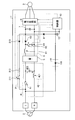
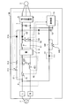
- FIG. 1 is a diagram illustrating a configuration of the power supply device according to the first embodiment.
- the power supply device 1 converts AC power supplied from the AC power source 2 into DC power, further converts DC power into AC power, and drives the motor 3 that is a load.
- the power supply device 1 includes an input unit 4 to which AC power is input from an AC power source 2.
- the input unit 4 includes a switch unit 41 having one end connected to one end of the AC power source 2, and a noise filter 42 connected to the other end of the switch unit 41 and the other end of the AC power source 2.
- a connection portion between one end of the AC power supply 2 and one end of the switch unit 41 is referred to as a terminal L, and a connection portion between the other end of the AC power supply 2 and the noise filter 42 is referred to as a terminal N.
- the noise filter 42 includes a coil 421 that is an inductive element and a capacitor 422 that is a capacitive element. One end of the coil 421 is connected to the terminal N. One end of the capacitor 422 is connected to the other end of the first switch unit 41. The other end of the capacitor 422 is connected to the other end of the coil 421.
- the switch unit 41 is in an off state at the initial time.
- the coil 421 may suppress leakage of normal mode high frequency noise, may suppress common mode noise, or may suppress both normal mode and common mode noise. It may be.
- the first switch unit 41 When the switch unit 41 is off, one end of the capacitor 422 and the terminal L are disconnected. Therefore, the first switch unit 41 has a function of suppressing reactive power generated when AC power is supplied to the capacitor 422.
- the power supply device 1 includes a first rectification unit 5 that converts AC power that has passed through the input unit 4 into DC power.
- the first rectifying unit 5 is exemplified by a diode bridge.
- the power supply device 1 improves the power factor of the DC power output from the first rectifying unit 5, reduces the power harmonics of the DC voltage output from the first rectifying unit 5, and the first rectifying unit 5 Includes a power factor correction unit 6 that boosts the DC voltage output from.
- the power factor improving unit 6 includes a reactor 61 that is an inductive element that has one end connected to the output terminal on the high potential side of the first rectifying unit 5 and stores energy due to the current that has passed through the first rectifying unit 5.
- the power factor improving unit 6 includes a semiconductor switch element 62 that has one end connected to the other end of the reactor 61 and causes a power supply short circuit to flow a short circuit current through the reactor 61.
- the power factor improving unit 6 includes a diode 63 that is a rectifying element that has an anode connected to the other end of the reactor 61 and supplies energy stored in the reactor 61 to the first power storage unit 7.
- the reactor 61, the semiconductor switch element 62, and the diode 63 constitute a boost chopper circuit.
- the power factor improvement unit 6 includes a current detection unit 64 that is connected between the semiconductor switch element 62 and the output terminal on the low potential side of the first rectification unit 5 and detects a current flowing through the semiconductor switch element 62.
- the power supply device 1 includes a first power storage unit 7 that stores the DC power that has passed through the power factor correction unit 6.
- the first power storage unit 7 is exemplified by a capacitor.
- the DC power stored in the first power storage unit 7 is supplied to the load side.
- the power supply device 1 includes a power conversion unit 8 that converts DC power stored in the first power storage unit 7 into AC power having a desired voltage and frequency and supplies the AC power to the motor 3.
- the power conversion unit 8 is exemplified by a three-phase inverter circuit.
- the power supply device 1 includes a charging unit 21 connected between the terminal N and one end on the high potential side of the first power storage unit 7.
- the charging unit 21 can store DC power in the first power storage unit 7 without going through the noise filter 42.
- the charging unit 21 includes a charging switch unit 211, a charging resistor 212 that is a resistive element, and a diode 213 that is a rectifying element.
- the charging switch unit 211 is in an off state at the initial time.
- the charging switch unit 211 When the charging switch unit 211 is in an on state, current flows through a path of the terminal L, the charging switch unit 211, the charging resistor 212, the diode 213, the first power storage unit 7 and the terminal N, and the first power storage unit 7 stores power. Is done.
- the charging resistor 212 has a function of suppressing an inrush current that flows when the first power storage unit 7 stores power. This eliminates the need for the power supply device 1 to connect the charging resistor to the switch unit 41 in parallel.
- the power supply device 1 includes a second rectification unit 11 that converts AC power of the AC power source 2 into DC power, and a second power storage unit 12 that stores DC power that has passed through the second rectification unit 11.
- the second rectifying unit 11 includes a diode 111 that is a rectifying element.
- the second power storage unit 12 is exemplified by a capacitor that is a capacitive element.
- the anode of the diode 111 is connected to the terminal L.
- the cathode of the diode 111 is connected to one end on the high potential side of the second power storage unit 12.
- the other end on the low potential side of the second power storage unit 12 is connected to the terminal N via the power factor improving unit 6, the first rectifying unit 5, and the input unit 4.
- the power supply device 1 includes a control unit 13 that controls the power conversion unit 8 while controlling the switch unit 41, the semiconductor switch element 62, and the charge switch unit 211 to be in an on state or an off state.
- the control unit 13 operates using DC power stored in the second power storage unit 12.
- the current detected by the current detection unit 64 in the power factor improvement unit 6 is input to the control unit 13.
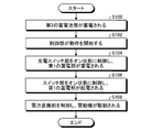
- FIG. 2 is a flowchart showing the operation of the power supply device according to the first embodiment.
- the power supply device 1 performs the operation shown in FIG.
- step S100 When AC power is supplied from the AC power supply 2 to the power supply device 1, in step S100, current flows through a path that passes through the terminal L, the second rectification unit 11, the second power storage unit 12, and the terminal N, and the second Is stored.
- the DC power is stored in the second power storage unit 12 only during a period in which the potential of the terminal L is higher than the potential of the terminal N. Therefore, the rectification operation by the second rectification unit 11 and the first rectification unit 5 is half-wave rectification.
- control unit 13 uses the DC power stored in the second power storage unit 12 to start operation in step S102. At this time, DC power is not stored in the first power storage unit 7.
- the control unit 13 controls the charging switch unit 211 to be on in step S104. As a result, a current flows through a path that passes through the terminal L, the charging switch unit 211, the charging resistor 212, the diode 213, the first power storage unit 7, and the terminal N, and the first power storage unit 7 is stored.
- the first power storage unit 7 When the first power storage unit 7 is stored, the first power storage unit 7 can supply power to the second power storage unit 12 via the diode 9.
- step S106 the control unit 13 controls the switch unit 41 to be in an on state. At this time, the control unit 13 controls the charging switch unit 211 to be turned off. As a result, the first power storage unit 7 is supplied with power through a path that passes through the noise filter 42, the first rectification unit 5, and the power factor conversion unit 6. Thereby, the leakage of high frequency noise by the noise filter 42 is suppressed, the power factor is improved by the on / off control of the semiconductor switch element 62, and the DC voltage is boosted.
- Control unit 13 starts control of power conversion unit 8 in step S108. Thereby, the electric motor 3 is driven.
- FIG. 3 is a flowchart of the operation of the power supply device according to the first embodiment.
- the control unit 13 executes the process shown in FIG. 3 during the control operation.
- the current detection unit 64 detects a short-circuit current.
- the control unit 13 determines whether or not a current greater than a predetermined threshold is detected by the current detection unit 64 in step S200. If it determines with the electric current detection part 64 not having detected the electric current larger than a threshold value (No), the control part 13 will wait by step S200.
- control part 13 determines with the electric current detection part 64 having detected the electric current larger than a threshold value (Yes), it will advance a process to step S202.
- step S202 the control unit 13 stops the control of the power conversion unit 8 and controls the switch unit 41 to the off state. Thereby, the power supply device 1 can suppress the failure of the power conversion unit 8 due to an excessive current or voltage.
- the control unit 13 does not stop the operation.
- the second rectifying unit 11 is configured by the diode 111 having the anode connected to the terminal L and the cathode connected to the second power storage unit 12.
- the second rectification unit 11 suppresses the path where the voltage of the capacitor 422 is superimposed on the second power storage unit 12. Therefore, the power supply device 1 does not have to make the withstand voltage of the second power storage unit 12 more than twice the voltage applied during normal operation. Thereby, the power supply device 1 can reduce the cost of the second power storage unit 12.
- the AC power of the AC power supply 2 is supplied to the second power storage unit 12 through a path that is unrelated to the short circuit failure of the semiconductor switch element 62. Thereby, the power supply device 1 can continue the operation without stopping the operation of the control unit 13.
- Embodiment 2 an inrush current flows through the second rectification unit 11 at the start of power storage in the second power storage unit 12 via the second rectification unit 11.
- the diode 111 may possibly fail. Therefore, in order to reduce the size of the diode 111, it is necessary to suppress the inrush current.
- the inrush current to the diode 111 is suppressed.
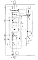
- FIG. 4 is a diagram illustrating a configuration of the power supply device according to the second embodiment.
- the power supply device 1A is controlled by the control unit 13 and the second charging resistor 141 connected in series with the second rectifying unit 11 when current flows in the configuration of the power supply device 1 according to the first embodiment. It further includes a second charging switch unit 142 that switches the path of the current flowing through the second rectifying unit 11 to a path that passes through the second charging resistor 141 or a path that does not pass through the second charging resistor 141.
- One end of the second charging resistor 141 is connected to the terminal L.
- One end of the second charge switch unit 142 is connected to the anode of the diode 111.
- the other end of the second charging switch unit 142 is switched and connected to a contact A on one end side of the second charging resistor 141 or a contact B on the other end side of the second charging resistor 141.
- the second charging switch unit 142 is connected to the contact B side at the initial time.
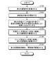
- FIG. 5 is a flowchart of the operation of the power supply device according to the second embodiment.
- power supply device 1 ⁇ / b> A performs the operation shown in FIG. 5.
- Steps S100, S102, S104, S106, and S108 in the flowchart shown in FIG. 5 are the same as those in the flowchart shown in FIG. 2 according to the first embodiment.
- the flowchart shown in FIG. 5 includes step S103 between step S102 and step S104.
- step S100 When AC power is supplied from the AC power source 2 to the power source device 1, in step S100, the terminal L, the second charging resistor 141, the second charging switch unit 142, the second rectifying unit 11, and the second power storage unit. A current flows through a path passing through the terminal 12 and the terminal N, and the second power storage unit 12 is charged.
- control unit 13 starts operation using the DC power stored in the second power storage unit 12 in step S102.
- Step S103 the control unit 13 performs control to switch the second charge switch unit 142 so that the other end of the second charge switch unit 142 is connected to the contact A.
- the control unit 13 causes the terminal L, the second charging switch unit 142, the second rectifying unit 11, the second path of the current that stores the second power storage unit 12 not to pass through the second charging resistor 141, 2 is routed through the power storage unit 12 and the terminal N.
- step S ⁇ b> 103 the supply of DC power to the second power storage unit 12 is performed through a path that does not pass through the second charging resistor 141, thereby suppressing power loss in the second charging resistor 141.
- step S104 and subsequent steps are the same as those in the first embodiment, description thereof is omitted.
- the power supply device 1A can reduce the size of the diode 111 of the second rectifying unit 11. Therefore, the power supply device 1A can reduce the cost of the second rectification unit 11.
- the control unit 13 starts operation using the DC power stored in the second power storage unit 12
- the second charge switch unit 142 is connected to the contact A so that the other end of the second charge switch unit 142 is connected to the second power supply unit 12.
- Control to switch the charging switch unit 142 is performed.
- the control unit 13 causes the terminal L, the second charging switch unit 142, the second rectifying unit 11, the second path of the current that stores the second power storage unit 12 not to pass through the second charging resistor 141, 2 is routed through the power storage unit 12 and the terminal N. Therefore, the power supply device 1A can suppress power loss in the second charging resistor 141.
- the arrangement of the second charging resistor 141 may be connected in series with the second rectifying unit 11 when a current flows through the second charging resistor 141.
- the second charging resistor 141 may be disposed between the second rectifying unit 11 and the second power storage unit 12.
- connection between the second charging resistor 141 and the second charging switch unit 142 is not limited to the configuration shown in FIG.
- FIG. 6 is a diagram illustrating a configuration of another example of the power supply device according to the second embodiment.
- the second charging resistor 141 is connected in series between the second rectifying unit 11 and the second power storage unit 12.
- the second charging switch unit 142 is connected in parallel to the second charging resistor 141.
- the second charging switch unit 142 is in an off state at the initial time.
- control unit 13 uses the DC power stored in the second power storage unit 12 to start operation.
- the control part 13 will perform control which switches the 2nd charge switch part 142 to an ON state, if operation
- the supply of DC power to the second power storage unit 12 is performed through a path that passes through the second rectification unit 11 during a period in which DC power is not stored in the first power storage unit 7. Then, the supply of DC power to the second power storage unit 12 is performed through a path that does not pass through the second charging resistor 141, thereby suppressing power loss in the second charging resistor 141.
- the power supply device 1B can reduce the size of the diode 111 of the second rectifying unit 11. Therefore, the power supply device 1B can reduce the cost of the second rectification unit 11.
- control unit 13 when the control unit 13 starts operation using the DC power stored in the second power storage unit 12, the control unit 13 performs control to switch the second charge switch unit 142 to the on state. Thereby, the control unit 13 causes the terminal L, the second charging switch unit 142, the second rectifying unit 11, the second path of the current that stores the second power storage unit 12 not to pass through the second charging resistor 141, 2 is routed through the power storage unit 12 and the terminal N. Therefore, the power supply device 1B can suppress power loss in the second charging resistor 141.
- the arrangement of the second charging resistor 141 may be in series with the second rectifying unit 11. Specifically, the arrangement of the second charging resistor 141 may be between the terminal L and the second rectifying unit 11.
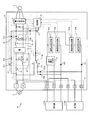
- FIG. 7 is a diagram illustrating a configuration of the air-conditioning apparatus according to the third embodiment.
- the air conditioner 30 includes a power supply device 1C and indoor units 31A and 31B.
- the power supply device 1C is obtained by adding a circuit for connecting to the indoor units 31A and 31B to the configuration of the power supply device 1B according to the second embodiment.
- the power supply device 1C includes an indoor unit connection unit 33 including a plurality of terminals to which the indoor units 31A and 31B are connected, and a communication circuit transmission unit 52A for communicating with the indoor units 31A and 31B.
- the indoor unit connection unit 33 includes terminals S1, S2, S3, S4, S5 and S6.
- the terminal S1 is connected to the terminal L, and the terminal S2 is connected to the terminal N.
- the indoor unit 31A is supplied with AC power via terminals S1 and S2.
- the terminal S4 is connected to the terminal L via the terminal S1, and the terminal S5 is connected to the terminal N via the terminal S2.
- the indoor unit 31B is supplied with AC power via terminals S4 and S5.
- the communication power generation unit 51 generates power to be used by the communication circuit transmission units 52A and 53A and the communication circuit reception units 52B and 53B using an AC power supplied via the terminals S1 and S2.
- the anode of the diode 52C is connected to the communication circuit receiver 52B, and the cathode is connected to the terminal S3.
- the diode 53C has an anode connected to the communication circuit receiving unit 53B and a cathode connected to the terminal S6.
- the anode of the diode 52D is connected to the terminal S3.
- the anode of the diode 53D is connected to the terminal S6.
- the cathode of the diode 52D and the cathode of the diode 53D are connected in common and connected to one end of the second charging resistor 141.
- one end of the second charging resistor 141 is not connected to the terminal L.
- FIG. 8 is a flowchart showing the operation of the air-conditioning apparatus according to the third embodiment.
- the first power storage unit 7 and the second power storage unit 12 are not formed with a current path for storing DC power.
- the second power storage unit 12 does not store DC power.
- the controller 13 does not start operation because no power is supplied. Therefore, the other end of the second charging switch 142 remains in the initial state where it is connected to the terminal B on the second charging resistor 141 side.
- power is supplied to the indoor unit 31A via terminals S1 and S2, and power is supplied to the indoor unit 31B via terminals S4 and S5.
- the indoor unit 31A short-circuits the terminal S1 and the terminal S3 in the indoor unit connection unit 33 by connecting a contact provided in the indoor unit 31A in step S300. I do.
- the indoor unit 31B performs control to short-circuit the terminal S4 and the terminal S6 in the indoor unit connection unit 33 by connecting a contact provided in the indoor unit 31B.
- step S302 When the terminal S1 and the terminal S3 in the indoor unit connection unit 33 are short-circuited, in step S302, the terminal L, the terminal S1, the terminal S3, the diode 52D, the second charging resistor 141, the second rectifying unit 11, the second Current flows through a path passing through the power storage unit 12 and the terminal N, and the second power storage unit 12 is charged.
- step S302 when the terminal S4 and the terminal S6 in the indoor unit connection unit 33 are short-circuited, in step S302, the terminal L, the terminal S4, the terminal S6, the diode 53D, the second charging resistor 141, the second rectifying unit 11, A current flows through a path passing through the second power storage unit 12 and the terminal N, and the second power storage unit 12 is stored.
- control unit 13 uses the DC power stored in the second power storage unit 12 to start operation in step S304.
- step S306 the control unit 13 performs control to switch the second charge switch unit 142 so that the other end of the second charge switch unit 142 is connected to the contact A.
- the control unit 13 causes the terminal L, the second charging switch unit 142, the second rectifying unit 11, the second path of the current that stores the second power storage unit 12 not to pass through the second charging resistor 141, 2 is routed through the power storage unit 12 and the terminal N.
- step S306 The supply of DC power to the second power storage unit 12 is performed through a path that passes through the second rectification unit 11 during a period in which DC power is not stored in the first power storage unit 7.
- step S306 the supply of DC power to the second power storage unit 12 is performed through a path that does not pass through the second charging resistor 141, so that power loss in the second charging resistor 141 is suppressed.
- step S308 the indoor unit 31A opens a contact provided in the indoor unit 31A in order to exchange communication signals with the control unit 13 via the terminal S3. An operation of opening the terminals S1 and S3 is performed.
- the indoor unit 31B opens the contact provided in the indoor unit 31B in order to exchange communication signals with the control unit 13 via the terminal S6, whereby the indoor unit connection unit 33 is opened. An operation of opening the terminal S4 and the terminal S6 is performed.
- the current path for storing the second power storage unit 12 is formed so as to pass through the terminal L, the second charge switch unit 142, the second rectification unit 11, the second power storage unit 12, and the terminal N. Therefore, the control unit 13 can continue the operation.
- Steps S310, S312 and S314 are the same as steps S104, S106 and S108 in FIG.
- the air conditioner 30 includes the power supply device 1C and the indoor units 31A and 31B, and transmits and receives communication signals between the indoor units 31A and 31B and the control unit 13.
- the diodes 52D and 53D are connected to the circuit to be performed, and the cathodes of the diodes 52D and 53D are connected to the second charging resistor 141.
- the control unit 13 switches the contact point of the second charging switch unit 142 to form a path for supplying DC power from the terminal L to the second power storage unit 12, so that the interiors of the subsequent indoor units 31A and 31B The operation can be continued regardless of the operation of the contact.
- the configuration described in the above embodiment shows an example of the contents of the present invention, and can be combined with another known technique, and can be combined with other configurations without departing from the gist of the present invention. It is also possible to omit or change the part.
- 1, 1A, 1B, 1C power supply device 2 AC power supply, 3 motor, 4 input unit, 5 first rectification unit, 6 power factor improvement unit, 7 first power storage unit, 8 power conversion unit, 11 second Rectification unit, 12 second power storage unit, 13 control unit, 30 air conditioner, 31A, 31B indoor unit.
Landscapes
- Engineering & Computer Science (AREA)
- Power Engineering (AREA)
- Physics & Mathematics (AREA)
- Electromagnetism (AREA)
- Chemical & Material Sciences (AREA)
- Combustion & Propulsion (AREA)
- Mechanical Engineering (AREA)
- General Engineering & Computer Science (AREA)
- Rectifiers (AREA)
- Charge And Discharge Circuits For Batteries Or The Like (AREA)
- Air Conditioning Control Device (AREA)
Abstract
Description
図1は、実施の形態1にかかる電源装置の構成を示す図である。電源装置1は、交流電源2から供給される交流電力を直流電力に変換し、更に直流電力を交流電力に変換して、負荷である電動機3を駆動する。
実施の形態1では、第2の整流部11を経由しての第2の蓄電部12への蓄電開始時に、第2の整流部11に突入電流が流れる。第2の整流部11内のダイオード111に大きな突入電流が流れると、ダイオード111が故障に至る可能性がある。従って、ダイオード111の小型化を図るためには、突入電流の抑制を図る必要がある。実施の形態2は、ダイオード111への突入電流の抑制を図るものである。
図7は、実施の形態3にかかる空気調和装置の構成を示す図である。空気調和装置30は、電源装置1Cと、室内機31A及び31Bと、を含む。
Claims (7)
- 交流電源から交流電力が入力される入力部と、
前記入力部を通過した交流電力を直流電力に変換する第1の整流部と、
前記第1の整流部から出力される直流電力の力率を改善する力率改善部と、
前記力率改善部を通過した直流電力を蓄電し、蓄電した直流電力を負荷側に供給する第1の蓄電部と、
前記入力部が前記交流電源に接続する部分に接続され、交流電力を直流電力に変換する第2の整流部と、
前記第2の整流部を通過した直流電力を蓄電する第2の蓄電部と、
前記第2の蓄電部に蓄電された電力を使用して動作し、前記力率改善部で短絡故障が発生したら、前記入力部を遮断する制御を行う制御部と、
を備えることを特徴とする電源装置。 - 前記入力部は、
一端が前記交流電源の一端に接続され、前記制御部によってオン状態又はオフ状態に制御されるスイッチ部と、
スイッチ部の他端及び交流電源の他端に接続されたノイズフィルタと、
を含むことを特徴とする、請求項1に記載の電源装置。 - 電流が流れるときに前記第2の整流部と直列に接続され、電流のピーク値を抑制する充電抵抗を更に備えることを特徴とする、請求項1又は2に記載の電源装置。
- 前記制御部によって制御され、前記第2の整流部に流れる電流の経路を、前記充電抵抗を経由する経路又は前記充電抵抗を経由しない経路に切り換える充電スイッチ部を更に備え、
前記制御部は、
前記第2の蓄電部に蓄電された直流電力を使用して動作を開始したら、前記第2の整流部に流れる電流の経路が前記充電抵抗を経由しない経路になるように、前記充電スイッチ部を切り換える制御を行う
ことを特徴とする、請求項3に記載の電源装置。 - 電源装置と室内機とを含む空気調和装置であって、
前記電源装置は、
交流電源から交流電力が入力される入力部と、
前記入力部を通過した交流電力を直流電力に変換する第1の整流部と、
前記第1の整流部から出力される直流電力の力率を改善する力率改善部と、
前記力率改善部を通過した直流電力を蓄電し、蓄電した直流電力を負荷側に供給する第1の蓄電部と、
電流のピーク値を抑制する充電抵抗と、
交流電力を直流電力に変換する第2の整流部と、
前記充電抵抗と前記第2の整流部との間又は前記入力部が前記交流電源に接続する部分と前記第2の整流部との間を接続する充電スイッチ部と、
前記第2の整流部を通過した直流電力を蓄電する第2の蓄電部と、
前記第2の蓄電部に蓄電された電力を使用して動作し、前記力率改善部で短絡故障が発生したら、前記入力部を遮断する制御を行う制御部と、
を備え、
前記室内機は、
運転を開始するときに、前記充電抵抗に電流を流す制御を行う
ことを特徴とする空気調和装置。 - 前記充電スイッチ部は、前記制御部が動作しないときは、前記室内機と通信する通信回路と前記第2の整流部とを接続する
ことを特徴とする、請求項5に記載の空気調和装置。 - 前記制御部は、
前記第2の蓄電部に蓄電された直流電力を使用して動作を開始したら、前記入力部が前記交流電源に接続する部分と前記第2の整流部との間を接続するように、前記充電スイッチ部を切り換える制御を行う
ことを特徴とする、請求項5又は6に記載の空気調和装置。
Priority Applications (7)
| Application Number | Priority Date | Filing Date | Title |
|---|---|---|---|
| JP2017508948A JP6366820B2 (ja) | 2015-03-31 | 2015-03-31 | 電源装置及び空気調和装置 |
| AU2015389440A AU2015389440B2 (en) | 2015-03-31 | 2015-03-31 | Power supply device and air-conditioning device |
| SG11201706701SA SG11201706701SA (en) | 2015-03-31 | 2015-03-31 | Power supply device and air conditioner |
| PCT/JP2015/060220 WO2016157441A1 (ja) | 2015-03-31 | 2015-03-31 | 電源装置及び空気調和装置 |
| US15/550,506 US10063133B2 (en) | 2015-03-31 | 2015-03-31 | Power supply device and air conditioner |
| CN201580075822.9A CN107210682B (zh) | 2015-03-31 | 2015-03-31 | 电源装置以及空气调节装置 |
| EP15866372.4A EP3101797B1 (en) | 2015-03-31 | 2015-03-31 | Power supply device and air-conditioning device |
Applications Claiming Priority (1)
| Application Number | Priority Date | Filing Date | Title |
|---|---|---|---|
| PCT/JP2015/060220 WO2016157441A1 (ja) | 2015-03-31 | 2015-03-31 | 電源装置及び空気調和装置 |
Publications (1)
| Publication Number | Publication Date |
|---|---|
| WO2016157441A1 true WO2016157441A1 (ja) | 2016-10-06 |
Family
ID=57006875
Family Applications (1)
| Application Number | Title | Priority Date | Filing Date |
|---|---|---|---|
| PCT/JP2015/060220 WO2016157441A1 (ja) | 2015-03-31 | 2015-03-31 | 電源装置及び空気調和装置 |
Country Status (7)
| Country | Link |
|---|---|
| US (1) | US10063133B2 (ja) |
| EP (1) | EP3101797B1 (ja) |
| JP (1) | JP6366820B2 (ja) |
| CN (1) | CN107210682B (ja) |
| AU (1) | AU2015389440B2 (ja) |
| SG (1) | SG11201706701SA (ja) |
| WO (1) | WO2016157441A1 (ja) |
Cited By (2)
| Publication number | Priority date | Publication date | Assignee | Title |
|---|---|---|---|---|
| WO2019077842A1 (ja) * | 2017-10-17 | 2019-04-25 | 三菱重工サーマルシステムズ株式会社 | 電力変換装置、電動機駆動装置及び空気調和装置 |
| WO2020053986A1 (ja) * | 2018-09-12 | 2020-03-19 | 三菱電機株式会社 | 空気調和システム |
Families Citing this family (6)
| Publication number | Priority date | Publication date | Assignee | Title |
|---|---|---|---|---|
| JP7113228B2 (ja) * | 2016-08-31 | 2022-08-05 | パナソニックIpマネジメント株式会社 | 車両用蓄電装置 |
| WO2019016026A1 (en) * | 2017-07-17 | 2019-01-24 | Npc Tech Aps | DC-DC POWER CONVERTER WITH ENHANCED OUTPUT CURRENT RESOLUTION |
| US10746186B2 (en) * | 2017-08-04 | 2020-08-18 | Lennox Industries Inc. | HVAC blower protection |
| JP7199011B2 (ja) * | 2018-11-30 | 2023-01-05 | パナソニックIpマネジメント株式会社 | 負荷制御装置 |
| JP2022052795A (ja) * | 2020-09-24 | 2022-04-05 | 株式会社Subaru | 車両用電源装置 |
| CN112383217B (zh) * | 2020-11-10 | 2021-12-28 | 珠海格力电器股份有限公司 | 一种直流母线充电电路及其控制方法 |
Citations (7)
| Publication number | Priority date | Publication date | Assignee | Title |
|---|---|---|---|---|
| JPH048174A (ja) * | 1990-04-24 | 1992-01-13 | Matsushita Electric Works Ltd | 電源装置 |
| JP2000014155A (ja) * | 1998-06-26 | 2000-01-14 | Matsushita Electric Ind Co Ltd | 電源回路およびそれを用いた空気調和機 |
| JP2000262060A (ja) * | 1999-03-09 | 2000-09-22 | Canon Inc | 力率改善型電源装置及びその異常時制御方法 |
| JP2003274660A (ja) * | 2002-03-18 | 2003-09-26 | Origin Electric Co Ltd | スイッチング電源回路 |
| JP2012177500A (ja) | 2011-02-25 | 2012-09-13 | Daikin Industries Ltd | 電源回路およびヒートポンプユニット |
| JP2013050223A (ja) * | 2011-08-30 | 2013-03-14 | Fujitsu General Ltd | 空調機システム |
| JP2014217119A (ja) * | 2013-04-23 | 2014-11-17 | 新電元工業株式会社 | 電力供給回路、半導体集積回路、絶縁型スイッチング電源 |
Family Cites Families (19)
| Publication number | Priority date | Publication date | Assignee | Title |
|---|---|---|---|---|
| DE3830460A1 (de) * | 1988-09-08 | 1990-03-15 | Asea Brown Boveri | Schaltungsanordnung zur speisung eines elektrischen verbrauchers aus einem wechselspannungsnetz |
| JP2705303B2 (ja) | 1990-11-15 | 1998-01-28 | 株式会社村田製作所 | 電源回路 |
| JPH04299070A (ja) * | 1991-03-26 | 1992-10-22 | Hitachi Ltd | スイッチングレギュレータ |
| JPH09233807A (ja) | 1996-02-29 | 1997-09-05 | Toshiba Corp | 電源装置 |
| JP2000197347A (ja) * | 1998-12-25 | 2000-07-14 | Hitachi Ltd | 電源装置 |
| JP2001268917A (ja) | 2000-03-22 | 2001-09-28 | Fuji Electric Co Ltd | 直流電源装置 |
| JP2005210809A (ja) * | 2004-01-21 | 2005-08-04 | Toshiba Corp | 電気機器の電源装置 |
| DE102004012215B4 (de) * | 2004-03-12 | 2020-03-26 | Tridonic Gmbh & Co Kg | Ansteuerung von Leuchtmittel-Betriebsgeräten mit einem zentralen kaskadierten AC/DC-Konverter |
| JP2008061309A (ja) | 2006-08-29 | 2008-03-13 | Mitsubishi Electric Corp | 電源回路及び放電灯点灯装置 |
| JP2009038848A (ja) * | 2007-07-31 | 2009-02-19 | Panasonic Corp | 電源回路 |
| US8085563B2 (en) * | 2009-02-12 | 2011-12-27 | Polar Semiconductor, Inc. | Protection and clamp circuit for power factor correction controller |
| CN201717818U (zh) * | 2010-06-09 | 2011-01-19 | 深圳市特尔佳科技股份有限公司 | 一种电涡流缓速器驱动控制器 |
| JP5264849B2 (ja) * | 2010-09-27 | 2013-08-14 | 三菱電機株式会社 | 電力変換装置及び冷凍空気調和装置 |
| JP5724451B2 (ja) | 2011-02-24 | 2015-05-27 | 三菱電機株式会社 | 電源装置及び空気調和装置 |
| WO2012120600A1 (ja) * | 2011-03-04 | 2012-09-13 | 三菱電機株式会社 | 電力変換装置および冷凍空調システム |
| KR101327070B1 (ko) * | 2011-12-22 | 2013-11-07 | 엘지이노텍 주식회사 | 돌입 전류 제한 회로 |
| WO2013112981A1 (en) * | 2012-01-26 | 2013-08-01 | Cameron D Kevin | Circuit for transferring power between a direct current line and an alternating-current line |
| JP6070263B2 (ja) * | 2013-02-26 | 2017-02-01 | 住友電気工業株式会社 | Dc−ac変換装置及び制御回路 |
| WO2020025935A1 (en) | 2018-08-03 | 2020-02-06 | Izzifix Limited | A connection system for connecting a conduit to a wall |
-
2015
- 2015-03-31 EP EP15866372.4A patent/EP3101797B1/en active Active
- 2015-03-31 AU AU2015389440A patent/AU2015389440B2/en active Active
- 2015-03-31 WO PCT/JP2015/060220 patent/WO2016157441A1/ja active Application Filing
- 2015-03-31 JP JP2017508948A patent/JP6366820B2/ja active Active
- 2015-03-31 CN CN201580075822.9A patent/CN107210682B/zh active Active
- 2015-03-31 SG SG11201706701SA patent/SG11201706701SA/en unknown
- 2015-03-31 US US15/550,506 patent/US10063133B2/en active Active
Patent Citations (7)
| Publication number | Priority date | Publication date | Assignee | Title |
|---|---|---|---|---|
| JPH048174A (ja) * | 1990-04-24 | 1992-01-13 | Matsushita Electric Works Ltd | 電源装置 |
| JP2000014155A (ja) * | 1998-06-26 | 2000-01-14 | Matsushita Electric Ind Co Ltd | 電源回路およびそれを用いた空気調和機 |
| JP2000262060A (ja) * | 1999-03-09 | 2000-09-22 | Canon Inc | 力率改善型電源装置及びその異常時制御方法 |
| JP2003274660A (ja) * | 2002-03-18 | 2003-09-26 | Origin Electric Co Ltd | スイッチング電源回路 |
| JP2012177500A (ja) | 2011-02-25 | 2012-09-13 | Daikin Industries Ltd | 電源回路およびヒートポンプユニット |
| JP2013050223A (ja) * | 2011-08-30 | 2013-03-14 | Fujitsu General Ltd | 空調機システム |
| JP2014217119A (ja) * | 2013-04-23 | 2014-11-17 | 新電元工業株式会社 | 電力供給回路、半導体集積回路、絶縁型スイッチング電源 |
Non-Patent Citations (1)
| Title |
|---|
| See also references of EP3101797A4 |
Cited By (2)
| Publication number | Priority date | Publication date | Assignee | Title |
|---|---|---|---|---|
| WO2019077842A1 (ja) * | 2017-10-17 | 2019-04-25 | 三菱重工サーマルシステムズ株式会社 | 電力変換装置、電動機駆動装置及び空気調和装置 |
| WO2020053986A1 (ja) * | 2018-09-12 | 2020-03-19 | 三菱電機株式会社 | 空気調和システム |
Also Published As
| Publication number | Publication date |
|---|---|
| AU2015389440B2 (en) | 2018-08-09 |
| CN107210682B (zh) | 2019-07-19 |
| AU2015389440A1 (en) | 2017-09-07 |
| JPWO2016157441A1 (ja) | 2017-08-10 |
| SG11201706701SA (en) | 2017-10-30 |
| EP3101797B1 (en) | 2020-04-22 |
| US20180034361A1 (en) | 2018-02-01 |
| EP3101797A4 (en) | 2017-05-10 |
| EP3101797A1 (en) | 2016-12-07 |
| CN107210682A (zh) | 2017-09-26 |
| US10063133B2 (en) | 2018-08-28 |
| JP6366820B2 (ja) | 2018-08-01 |
Similar Documents
| Publication | Publication Date | Title |
|---|---|---|
| JP6366820B2 (ja) | 電源装置及び空気調和装置 | |
| EP1835607B1 (en) | Apparatus and method for supplying DC power source | |
| US20170358926A1 (en) | Photovoltaic Air-conditioning System and Photovoltaic Air Conditioner Having Same | |
| JP2011524732A (ja) | 電力入力を備えた回路構成及び電力入力回路を制御する動作方法 | |
| JP6460479B2 (ja) | 制御電源装置および蓄電システム | |
| JPWO2018193606A1 (ja) | 電力変換装置 | |
| JP2010519885A (ja) | 複数の交流/直流入力を備えたsmps回路、並びにコンピュータ電源及びラップトップ用アダプタへの本方法の適用 | |
| JP3829846B2 (ja) | 無停電電源装置 | |
| JP2014110666A (ja) | 放電制御システム及び放電装置 | |
| JP6728285B2 (ja) | 高圧インバータの初期充電システム及びその制御方法 | |
| JP3191097B2 (ja) | 無停電電源装置及びその充電制御方法 | |
| JP2016158353A (ja) | 電力変換装置 | |
| JP6268786B2 (ja) | パワーコンディショナ、パワーコンディショナシステムおよびパワーコンディショナの制御方法 | |
| JP2013090511A (ja) | 電力制御装置 | |
| US10295213B2 (en) | Air conditioning apparatus | |
| JP2009278780A (ja) | 全波整流回路 | |
| CN114001439A (zh) | 空调器及其控制装置和方法 | |
| JP2016010193A (ja) | 鉄道車両用電源回路 | |
| EP4039529B1 (en) | Electrically excited motor drive system integrated with obc, and electric vehicle | |
| JP4932604B2 (ja) | 電圧補償装置 | |
| US20230318429A1 (en) | Power conversion apparatus | |
| JP2017139910A (ja) | 電力変換装置 | |
| JP2011211813A (ja) | 充放電装置 | |
| KR20210137790A (ko) | 액티브 디커플링 동작을 수행하는 전력 변환 장치 | |
| EP4351828A1 (en) | Hybrid power welding system |
Legal Events
| Date | Code | Title | Description |
|---|---|---|---|
| REEP | Request for entry into the european phase |
Ref document number: 2015866372 Country of ref document: EP |
|
| WWE | Wipo information: entry into national phase |
Ref document number: 2015866372 Country of ref document: EP |
|
| 121 | Ep: the epo has been informed by wipo that ep was designated in this application |
Ref document number: 15866372 Country of ref document: EP Kind code of ref document: A1 |
|
| ENP | Entry into the national phase |
Ref document number: 2017508948 Country of ref document: JP Kind code of ref document: A |
|
| WWE | Wipo information: entry into national phase |
Ref document number: 15550506 Country of ref document: US |
|
| ENP | Entry into the national phase |
Ref document number: 2015389440 Country of ref document: AU Date of ref document: 20150331 Kind code of ref document: A |
|
| WWE | Wipo information: entry into national phase |
Ref document number: 11201706701S Country of ref document: SG |
|
| NENP | Non-entry into the national phase |
Ref country code: DE |