WO2016152195A1 - ヘテロ接合バイポーラトランジスタ用エピタキシャルウェハ及びヘテロ接合バイポーラトランジスタ - Google Patents
ヘテロ接合バイポーラトランジスタ用エピタキシャルウェハ及びヘテロ接合バイポーラトランジスタ Download PDFInfo
- Publication number
- WO2016152195A1 WO2016152195A1 PCT/JP2016/050697 JP2016050697W WO2016152195A1 WO 2016152195 A1 WO2016152195 A1 WO 2016152195A1 JP 2016050697 W JP2016050697 W JP 2016050697W WO 2016152195 A1 WO2016152195 A1 WO 2016152195A1
- Authority
- WO
- WIPO (PCT)
- Prior art keywords
- covalent bond
- bipolar transistor
- substitution site
- type impurity
- bond radius
- Prior art date
- Legal status (The legal status is an assumption and is not a legal conclusion. Google has not performed a legal analysis and makes no representation as to the accuracy of the status listed.)
- Ceased
Links
Images

Classifications
-
- H—ELECTRICITY
- H10—SEMICONDUCTOR DEVICES; ELECTRIC SOLID-STATE DEVICES NOT OTHERWISE PROVIDED FOR
- H10D—INORGANIC ELECTRIC SEMICONDUCTOR DEVICES
- H10D62/00—Semiconductor bodies, or regions thereof, of devices having potential barriers
- H10D62/10—Shapes, relative sizes or dispositions of the regions of the semiconductor bodies; Shapes of the semiconductor bodies
- H10D62/13—Semiconductor regions connected to electrodes carrying current to be rectified, amplified or switched, e.g. source or drain regions
- H10D62/137—Collector regions of BJTs
-
- H—ELECTRICITY
- H10—SEMICONDUCTOR DEVICES; ELECTRIC SOLID-STATE DEVICES NOT OTHERWISE PROVIDED FOR
- H10D—INORGANIC ELECTRIC SEMICONDUCTOR DEVICES
- H10D10/00—Bipolar junction transistors [BJT]
- H10D10/01—Manufacture or treatment
- H10D10/021—Manufacture or treatment of heterojunction BJTs [HBT]
-
- H—ELECTRICITY
- H10—SEMICONDUCTOR DEVICES; ELECTRIC SOLID-STATE DEVICES NOT OTHERWISE PROVIDED FOR
- H10D—INORGANIC ELECTRIC SEMICONDUCTOR DEVICES
- H10D10/00—Bipolar junction transistors [BJT]
- H10D10/80—Heterojunction BJTs
- H10D10/821—Vertical heterojunction BJTs
-
- H—ELECTRICITY
- H10—SEMICONDUCTOR DEVICES; ELECTRIC SOLID-STATE DEVICES NOT OTHERWISE PROVIDED FOR
- H10D—INORGANIC ELECTRIC SEMICONDUCTOR DEVICES
- H10D62/00—Semiconductor bodies, or regions thereof, of devices having potential barriers
- H10D62/80—Semiconductor bodies, or regions thereof, of devices having potential barriers characterised by the materials
- H10D62/85—Semiconductor bodies, or regions thereof, of devices having potential barriers characterised by the materials being Group III-V materials, e.g. GaAs
- H10D62/854—Semiconductor bodies, or regions thereof, of devices having potential barriers characterised by the materials being Group III-V materials, e.g. GaAs further characterised by the dopants
-
- H—ELECTRICITY
- H10—SEMICONDUCTOR DEVICES; ELECTRIC SOLID-STATE DEVICES NOT OTHERWISE PROVIDED FOR
- H10D—INORGANIC ELECTRIC SEMICONDUCTOR DEVICES
- H10D62/00—Semiconductor bodies, or regions thereof, of devices having potential barriers
- H10D62/80—Semiconductor bodies, or regions thereof, of devices having potential barriers characterised by the materials
- H10D62/85—Semiconductor bodies, or regions thereof, of devices having potential barriers characterised by the materials being Group III-V materials, e.g. GaAs
Definitions
- the present invention relates to an epitaxial wafer for compound semiconductor elements and a compound semiconductor element, and more particularly to an epitaxial wafer for heterojunction bipolar transistors and a heterojunction bipolar transistor.
- Heterojunction bipolar transistors are capable of ultra-high-speed operation with low distortion, and are mainly used for high-frequency power amplifiers (PAs) of transmitters in mobile phones and wireless local area networks (LANs). ; Power Amplifier).
- PAs high-frequency power amplifiers
- LANs wireless local area networks
- Power Amplifier Power Amplifier
- the heterojunction bipolar transistor is formed, for example, on a substrate made of semi-insulating GaAs and made of n-type GaAs, and is formed on the subcollector layer for taking out current to the outside, and on the subcollector layer and undoped
- This thin film multilayer structure can be formed by a method such as metal organic vapor phase epitaxy (MOVPE; Metal-Organic-Vapor-Phase Epitaxy, or MOCVD; Metal-Organic-Chemical-Vapor-Deposition) or molecular beam growth (MBE). it can.
- MOVPE metal organic vapor phase epitaxy
- MOCVD Metal-Organic-Vapor-Phase Epitaxy
- MBE molecular beam growth
- the metal organic chemical vapor deposition method heats and gasifies a solid or liquid organometallic raw material and supplies it to a substrate heated to a predetermined temperature, whereby it is thermally decomposed on the substrate.
- a thin film crystal is epitaxially grown on a substrate by a chemical reaction.
- the molecular beam growth method evaporates each constituent element of the thin film crystal from a separate crucible in an ultra vacuum and supplies the element on the substrate heated to a predetermined temperature in the form of a molecular beam.
- a thin film crystal is epitaxially grown.
- an epitaxial wafer for a heterojunction bipolar transistor in which a thin film multilayer structure is epitaxially grown on a substrate is completed, and subsequent pattern formation, etching, electrode (emitter electrode, base electrode, and collector electrode) formation, protective film
- a heterojunction bipolar transistor is completed through processing steps such as formation and packaging.
- High-performance mobile terminals such as smartphones use a large number of high-frequency power amplifiers with the recent development of multi-band, which improves the electrical usage efficiency of heterojunction bipolar transistors used as high-frequency power amplifiers. It has become very important to ensure battery sustainability by reducing power consumption.
- the turn-on voltage and the on-resistance In order to improve the electricity use efficiency of the heterojunction bipolar transistor and reduce the power consumption, it is essential to reduce the turn-on voltage and the on-resistance.
- a heterojunction bipolar transistor it is necessary to form a collector electrode on a subcollector layer exposed by removing the base layer and the base electrode by etching or the like. Therefore, the subcollector layer is formed along the substrate plane direction. A long distance conductive path is required.
- an object of the present invention is to provide an epitaxial wafer for a heterojunction bipolar transistor and a heterojunction bipolar transistor capable of reducing the resistance of a subcollector layer without reducing the current amplification factor.
- the present invention relates to an epitaxial wafer for a heterojunction bipolar transistor having a subcollector layer made of n-type GaAs, wherein the subcollector layer has an n-type having a smaller covalent bond radius than a substitution site.
- the heterojunction bipolar transistor epitaxial wafer contains an impurity and an n-type impurity having a larger covalent bond radius than a substitution site.
- the sub-collector layer has a total (A) + of the n-type impurity impurity concentration (A) having a smaller covalent bond radius than the substitution site and the n-type impurity impurity concentration (B) having a larger covalent bond radius than the substitution site.
- (B) is preferably 3 ⁇ 10 18 cm ⁇ 3 or more and 1 ⁇ 10 19 cm ⁇ 3 or less.
- the sub-collector layer has a ratio (A) / ratio of impurity concentration (A) of n-type impurity having a covalent bond radius smaller than that of the substitution site and impurity concentration (B) of n-type impurity having a covalent bond radius larger than that of the substitution site.
- (B) is preferably 2 or more and 5 or less.
- the subcollector layer has an n-type impurity having a smaller covalent bond radius than the substitution site and a larger covalent bond radius than the substitution site.
- This is a heterojunction bipolar transistor containing an n-type impurity.
- the sub-collector layer has a total (A) + of the n-type impurity impurity concentration (A) having a smaller covalent bond radius than the substitution site and the n-type impurity impurity concentration (B) having a larger covalent bond radius than the substitution site.
- (B) is preferably 3 ⁇ 10 18 cm ⁇ 3 or more and 1 ⁇ 10 19 cm ⁇ 3 or less.
- the sub-collector layer has a ratio (A) / ratio of impurity concentration (A) of n-type impurity having a covalent bond radius smaller than that of the substitution site and impurity concentration (B) of n-type impurity having a covalent bond radius larger than that of the substitution site.
- (B) is preferably 2 or more and 5 or less.
- a heterojunction bipolar transistor epitaxial wafer 100 includes a substrate 101 made of semi-insulating GaAs, and formed on the substrate 101 and made of n-type GaAs.
- the collector layer 103 formed on the subcollector layer 102 and made of n-type GaAs
- the base layer 104 formed on the collector layer 103 and made of p-type GaAs
- An emitter layer 105 made of n-type InGaP
- an emitter contact layer 106 made of n-type GaAs and formed on the emitter layer 105
- an n-type In x Ga 1 formed on the emitter contact layer 106 and an n-type In x Ga 1 formed on the emitter contact layer 106.
- a non-alloy contact layer 107 made of -x as (0 ⁇ x ⁇ 1 ), the Bei To have.
- the subcollector layer 102 contains an n-type impurity having a smaller covalent bond radius than the substitution site and an n-type impurity having a larger covalent bond radius than the substitution site.
- Examples of the n-type impurity having a covalent bond radius smaller than that of the substitution site include Si (Ga site), Se (As site), and S (As site). Examples of the n-type impurity having a larger covalent bond radius than the substitution site include Sn (Ga site) or Te (As site).
- an n-type impurity having a smaller covalent bond radius than the substitution site and an n-type impurity having a larger covalent bond radius than the substitution site for example, a combination of Si and Sn, a combination of Si and Te, a combination of Se and Te, A combination of Se and Sn, a combination of S and Te, or a combination of S and Sn is conceivable. Moreover, three or more types of combinations such as a combination of Si, Sn, and Te may be used.
- the n-type impurity is Si, SiH 4 or Si 2 H 6 is used as a raw material, and the n-type impurity is When Se is used, H 2 Se is used as a raw material.
- the n-type impurity is S, (CH 3 ) 2 S, (C 2 H 5 ) 2 S, (C 4 H 9 S) 2 , or H is used as the raw material.
- the heterojunction bipolar transistor epitaxial wafer 100 is subjected to several processing steps to form an emitter electrode 201, a base electrode 202, and a collector electrode 203 as shown in FIG. can do.
- the subcollector layer 102 contains two types of n-type impurities having a covalent bond radius smaller than that of the substitution site and n-type impurities having a covalent bond radius larger than that of the substitution site.
- a subcollector layer made of n-type GaAs contains only one type of n-type impurity.
- Si when the subcollector layer contains Si as an n-type impurity, Si has a covalent bond radius at the substitution position. Therefore, when Si is added at a high concentration, tensile stress acts in the thin film crystal, and vacancy defects are likely to occur. In addition, when Si is added at a higher concentration, it is presumed that vacancy defects propagate to the base layer, and as a result, the current amplification factor is reduced.
- the present inventors have replaced, for example, Sn in the subcollector layer in addition to Si to replace vacancy defects due to Si having a small covalent bond radius with respect to Ga at the substitution position. Compensation was carried out with Sn having a large covalent bond radius with respect to Ga at the position, and the inventors came up with the idea that the tensile stress in the thin film crystal is greatly reduced.
- subcollector layer 102 contains two types of n-type impurities having a covalent bond radius smaller than that of the substitution site and n-type impurities having a covalent bond radius larger than that of the substitution site.
- the subcollector layer 102 includes the sum of the impurity concentration (A) of the n-type impurity having a covalent bond radius smaller than that of the substitution site and the impurity concentration (B) of the n-type impurity having a covalent bond radius larger than that of the substitution site (A ) + (B) is 3 ⁇ 10 18 cm ⁇ 3 or more and 1 ⁇ 10 19 cm ⁇ 3 or less, more preferably 4 ⁇ 10 18 cm ⁇ 3 or more and 1 ⁇ 10 19 cm ⁇ 3 or less.
- the sum (A) + (B) of the impurity concentration (A) of the n-type impurity having a smaller covalent bond radius than the substitution site and the impurity concentration (B) of the n-type impurity having a larger covalent bond radius than the substitution site is 3 ⁇ . This is because if it is less than 10 18 cm ⁇ 3 , the carrier concentration of the subcollector layer 102 cannot be increased as compared with the conventional case, and the resistance of the subcollector layer 102 cannot be decreased as compared with the conventional case.
- the sum (A) + (B) of the impurity concentration (A) of the n-type impurity having a covalent bond radius smaller than that of the substitution site and the impurity concentration (B) of the n-type impurity having a covalent bond radius larger than that of the substitution site is This is because if it exceeds 1 ⁇ 10 19 cm ⁇ 3 , it approaches the solid solution limit of impurities with respect to GaAs constituting the subcollector layer 102 and it becomes difficult to add impurities at a higher concentration. Even if the solid solution limit is not reached, if the doping is performed at a high concentration, the effect of generating defects and compensating the carrier works, so that the effect cannot be obtained.
- the subcollector layer 102 has a ratio (A) of the impurity concentration (A) of the n-type impurity having a covalent bond radius smaller than that of the substitution site and the impurity concentration (B) of the n-type impurity having a covalent bond radius larger than that of the substitution site.
- ) / (B) is 2 or more and 5 or less, more preferably 2 or more and 3 or less.
- n-type impurity having a covalent bond radius smaller than that of the substitution site for example, Si (Ga site), Se (As site), or S (As site), n-type having a larger covalent bond radius than the substitution site
- Te (As site) may be adopted as the impurity.
- (C 2 H 5 ) 2 Te, which is a raw material of Se, and H 2 Se, which is a raw material of Se are compared with (CH 3 ) 2 S, which is a raw material of Si, S 2 H 6 and S. Therefore, when the combination of these raw materials is adopted, the total impurity concentration (A) + (B) becomes as large as possible and the ratio (A) / (B).
- the growth temperature should be selected so that the value falls within the above numerical range.
- the impurity concentration (A) of the n-type impurity having a smaller covalent bond radius than the substitution site and the impurity of the n-type impurity having a larger covalent bond radius than the substitution site A total (A) + (B) with a concentration (B) of about 3 ⁇ 10 18 cm ⁇ 3 and a ratio (A) / (B) of 2 to 5 can be produced.
- the effect of the present invention can be obtained.
- the heterojunction bipolar transistor 200 is used not only for high-frequency power amplifiers for high-performance portable terminals, but also for low-output power amplifiers for Wi-Fi, which conventionally used high electron mobility transistors (HEMTs). Can be used.
- HEMTs high electron mobility transistors
- a sub-collector layer made of n-type GaAs, a collector layer made of n-type GaAs, a base layer made of p-type GaAs, an emitter layer made of n-type InGaP, and an n-type GaAs An epitaxial contact for a heterojunction bipolar transistor is formed by sequentially epitaxially growing an emitter contact layer and a non-alloy contact layer made of n-type In x Ga 1-x As (0 ⁇ x ⁇ 1) on a substrate made of semi-insulating GaAs. Was made.
- Si (Si 2 H 6 ) and Sn ((CH 3 ) 4 Sn) were used as a combination of n-type impurity raw materials having similar growth temperatures with good addition efficiency. Then, by changing the ratio between the Si impurity concentration and the Sn impurity concentration, a plurality of epitaxial wafers for heterojunction bipolar transistors having different total impurity concentrations were fabricated.
- heterojunction bipolar transistor was fabricated by performing several processing steps on the epitaxial wafer for the heterojunction bipolar transistor.
- (A) + (B) is 3 ⁇ 10 18 cm ⁇ 3 or more and 1 ⁇ 10 19 cm ⁇ 3 or less, and the impurity concentration (A) of the n-type impurity having a smaller covalent bond radius than the substitution site and the substitution site
- the ratio (A) / (B) to the impurity concentration (B) of the n-type impurity having a large covalent bond radius is 2 or more and 5 or less, the resistance of the subcollector layer is lowered and the decrease in the current amplification factor is suppressed. It was confirmed that the effects of the present invention can be exhibited.
Landscapes
- Bipolar Transistors (AREA)
Abstract
電流増幅率を低下させること無しにサブコレクタ層の抵抗を低下させることが可能なヘテロ接合バイポーラトランジスタ用エピタキシャルウェハ及びヘテロ接合バイポーラトランジスタを提供する。 n型GaAsからなるサブコレクタ層102を備えるヘテロ接合バイポーラトランジスタ用エピタキシャルウェハ100において、サブコレクタ層102は、置換サイトよりも共有結合半径が小さいn型不純物と置換サイトよりも共有結合半径が大きいn型不純物とを含有しているものである。
Description
本発明は、化合物半導体素子用エピタキシャルウェハ及び化合物半導体素子に係り、特に、ヘテロ接合バイポーラトランジスタ用エピタキシャルウェハ及びヘテロ接合バイポーラトランジスタに関する。
ヘテロ接合バイポーラトランジスタ(HBT;Heterojunction Bipolar Transistor)は、低歪で超高速動作が可能であり、主に携帯電話や無線ローカルエリアネットワーク(LAN;Local Area Network)等における送信部の高周波パワーアンプ(PA;Power Amplifier)として使用されている。
ヘテロ接合バイポーラトランジスタは、例えば、半絶縁性GaAsからなる基板上に形成されると共にn型GaAsからなり、外部に電流を取り出すためのサブコレクタ層と、サブコレクタ層上に形成されると共にアンドープ型GaAsやn型GaAsからなり、電子を集めるためのコレクタ層と、コレクタ層上に形成されると共にp型GaAsからなり、電子の流れを制御するためのベース層と、ベース層上に形成されると共にn型InGaPからなり、電子を放射するためのエミッタ層と、エミッタ層上に形成されると共にn型GaAsやn型InGaAsからなり、外部から電流を注入するためのエミッタコンタクト層と、を備える薄膜多層構造となっている。
この薄膜多層構造は、有機金属気相成長(MOVPE;Metal Organic Vapor Phase Epitaxy、又はMOCVD;Metal Organic Chemical Vapor Deposition)法や分子線成長(MBE;Molecular Beam Epitaxy)法等の方法により形成することができる。
このうち、有機金属気相成長法は、固体又は液体の有機金属原料を加熱してガス化させると共に所定の温度まで昇温させた基板上に供給することにより、これを基板上で熱分解乃至化学反応させて基板上に薄膜結晶をエピタキシャル成長させる方法である。
また、分子線成長法は、超真空中で薄膜結晶の構成元素のそれぞれを別々のルツボから蒸発させると共に分子線の形で所定の温度まで昇温させた基板上に供給することにより、基板上に薄膜結晶をエピタキシャル成長させる方法である。
但し、分子線成長法は、超真空環境が要求されることから、蒸気圧の高いP系のエピタキシャル成長が不得手であり、n型InGaPからなるベース層をエピタキシャル成長させる必要のあるヘテロ接合バイポーラトランジスタの場合、専ら有機金属気相成長法が採用されている。
これらの方法により、基板上に薄膜多層構造がエピタキシャル成長されてなるヘテロ接合バイポーラトランジスタ用エピタキシャルウェハが完成し、その後のパターン形成、エッチング、電極(エミッタ電極、ベース電極、及びコレクタ電極)形成、保護膜形成、及びパッケージング等の加工工程を経てヘテロ接合バイポーラトランジスタが完成する。
スマートフォン等の高性能携帯端末では、近年のマルチバンド化の進展に伴い多数の高周波パワーアンプが使用されていることから、高周波パワーアンプとして使用されているヘテロ接合バイポーラトランジスタの電気使用効率を向上させて消費電力を低減することにより、電池の持続性を確保することが非常に重要となってきている。
ヘテロ接合バイポーラトランジスタの電気使用効率を向上させて消費電力を低減するためには、ターンオン電圧やオン抵抗を低減することが必須となる。ヘテロ接合バイポーラトランジスタは、構造上、ベース層やベース電極をエッチング等で除去して露出させたサブコレクタ層上にコレクタ電極を形成する必要があるため、サブコレクタ層は、基板平面方向に沿って長距離導電路が必要となる。
よって、サブコレクタ層のキャリア濃度を増加させて抵抗を低下させることは、正にオン抵抗の低減に繋がるが、サブコレクタ層のキャリア濃度を増加させ過ぎると、電流増幅率が低下してしまい、必要十分なゲインが得られなくなるという問題がある。
そこで、本発明の目的は、電流増幅率を低下させること無しにサブコレクタ層の抵抗を低下させることが可能なヘテロ接合バイポーラトランジスタ用エピタキシャルウェハ及びヘテロ接合バイポーラトランジスタを提供することにある。
この目的を達成するために創案された本発明は、n型GaAsからなるサブコレクタ層を備えるヘテロ接合バイポーラトランジスタ用エピタキシャルウェハにおいて、前記サブコレクタ層は、置換サイトよりも共有結合半径が小さいn型不純物と置換サイトよりも共有結合半径が大きいn型不純物とを含有しているヘテロ接合バイポーラトランジスタ用エピタキシャルウェハである。
前記サブコレクタ層は、置換サイトよりも共有結合半径が小さいn型不純物の不純物濃度(A)と置換サイトよりも共有結合半径が大きいn型不純物の不純物濃度(B)との合計(A)+(B)が3×1018cm-3以上1×1019cm-3以下であると良い。
前記サブコレクタ層は、置換サイトよりも共有結合半径が小さいn型不純物の不純物濃度(A)と置換サイトよりも共有結合半径が大きいn型不純物の不純物濃度(B)との比(A)/(B)が2以上5以下であると良い。
また、本発明は、n型GaAsからなるサブコレクタ層を備えるヘテロ接合バイポーラトランジスタにおいて、前記サブコレクタ層は、置換サイトよりも共有結合半径が小さいn型不純物と置換サイトよりも共有結合半径が大きいn型不純物とを含有しているヘテロ接合バイポーラトランジスタである。
前記サブコレクタ層は、置換サイトよりも共有結合半径が小さいn型不純物の不純物濃度(A)と置換サイトよりも共有結合半径が大きいn型不純物の不純物濃度(B)との合計(A)+(B)が3×1018cm-3以上1×1019cm-3以下であると良い。
前記サブコレクタ層は、置換サイトよりも共有結合半径が小さいn型不純物の不純物濃度(A)と置換サイトよりも共有結合半径が大きいn型不純物の不純物濃度(B)との比(A)/(B)が2以上5以下であると良い。
以下、本発明の好適な実施の形態を添付図面にしたがって説明する。
図1に示すように、本発明の好適な実施の形態に係るヘテロ接合バイポーラトランジスタ用エピタキシャルウェハ100は、半絶縁性GaAsからなる基板101と、基板101上に形成されると共にn型GaAsからなるサブコレクタ層102と、サブコレクタ層102上に形成されると共にn型GaAsからなるコレクタ層103と、コレクタ層103上に形成されると共にp型GaAsからなるベース層104と、ベース層104上に形成されると共にn型InGaPからなるエミッタ層105と、エミッタ層105上に形成されると共にn型GaAsからなるエミッタコンタクト層106と、エミッタコンタクト層106上に形成されると共にn型InxGa1-xAs(0<x<1)からなるノンアロイコンタクト層107と、を備えている。
このヘテロ接合バイポーラトランジスタ用エピタキシャルウェハ100では、サブコレクタ層102は、置換サイトよりも共有結合半径が小さいn型不純物と置換サイトよりも共有結合半径が大きいn型不純物とを含有している。
置換サイトよりも共有結合半径が小さいn型不純物としては、例えば、Si(Gaサイト)、Se(Asサイト)、又はS(Asサイト)が挙げられる。また、置換サイトよりも共有結合半径が大きいn型不純物としては、例えば、Sn(Gaサイト)、又はTe(Asサイト)が挙げられる。
置換サイトよりも共有結合半径が小さいn型不純物と置換サイトよりも共有結合半径が大きいn型不純物の組み合わせとしては、例えば、SiとSnの組み合わせ、SiとTeの組み合わせ、SeとTeの組み合わせ、SeとSnの組み合わせ、SとTeの組み合わせ、又はSとSnの組み合わせが考えられる。また、SiとSnとTeの組み合わせのような3種類以上の組み合わせであっても良い。
なお、有機金属気相成長法を使用してサブコレクタ層102をエピタキシャル成長させる際には、例えば、n型不純物がSiのときは原料としてSiH4やSi2H6を使用し、n型不純物がSeのときは原料としてH2Seを使用し、n型不純物がSのときは原料として(CH3)2S、(C2H5)2S、(C4H9S)2、又はH2Sを使用し、n型不純物がSnのときは原料として(CH3)4Snや(C2H5)4Snを使用し、n型不純物がTeのときは原料として(CH3)2Teや(C2H5)2Teを使用する。
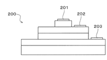
このヘテロ接合バイポーラトランジスタ用エピタキシャルウェハ100にいくつかの加工工程を施し、図2に示すように、エミッタ電極201、ベース電極202、及びコレクタ電極203を形成することにより、ヘテロ接合バイポーラトランジスタ200を作製することができる。
ここで、ヘテロ接合バイポーラトランジスタ用エピタキシャルウェハ100において、サブコレクタ層102が置換サイトよりも共有結合半径が小さいn型不純物と置換サイトよりも共有結合半径が大きいn型不純物の二種類を含有している理由を説明する。
通常、n型GaAsからなるサブコレクタ層はn型不純物を一種類だけ含有しているが、例えば、サブコレクタ層がn型不純物としてSiを含有している場合、Siは共有結合半径が置換位置のGaよりも小さいため、Siを高濃度に添加すると、薄膜結晶中に引張応力が働き、空孔欠陥が発生し易い。その上、Siをより高濃度に添加すると、空孔欠陥がベース層まで伝播し、その結果として、電流増幅率を低下させていると推測される。
そこで、本発明者等は、鋭意検討の結果、例えば、Siに加えてSnをサブコレクタ層に添加することで、置換位置のGaに対して共有結合半径が小さいSiによる空孔欠陥を、置換位置のGaに対して共有結合半径が大きいSnで補償し、薄膜結晶中の引張応力を大幅に低下させることに思い至った。
これにより、サブコレクタ層にn型不純物を高濃度に添加しても歪の極めて少ない、結晶状態の良好な薄膜結晶が得られるようになり、電流増幅率の低下を抑制することが可能となる。
従って、ヘテロ接合バイポーラトランジスタ用エピタキシャルウェハ100においては、サブコレクタ層102が置換サイトよりも共有結合半径が小さいn型不純物と置換サイトよりも共有結合半径が大きいn型不純物の二種類を含有している旨を規定した。
また、サブコレクタ層102は、置換サイトよりも共有結合半径が小さいn型不純物の不純物濃度(A)と置換サイトよりも共有結合半径が大きいn型不純物の不純物濃度(B)との合計(A)+(B)が3×1018cm-3以上1×1019cm-3以下、より好ましくは4×1018cm-3以上1×1019cm-3以下であることが望ましい。
置換サイトよりも共有結合半径が小さいn型不純物の不純物濃度(A)と置換サイトよりも共有結合半径が大きいn型不純物の不純物濃度(B)との合計(A)+(B)が3×1018cm-3未満であると、サブコレクタ層102のキャリア濃度を従来よりも増加させることができず、サブコレクタ層102の抵抗を従来よりも低下させることができないからである。
また、置換サイトよりも共有結合半径が小さいn型不純物の不純物濃度(A)と置換サイトよりも共有結合半径が大きいn型不純物の不純物濃度(B)との合計(A)+(B)が1×1019cm-3超であると、サブコレクタ層102を構成するGaAsに対する不純物の固溶限界に近づくため、それ以上の濃度で不純物を添加することが困難となるからである。また、固溶限界に達しなくても、高濃度にドーピングすると、欠陥を生成してキャリアを補償する力が働くので、効果が得られなくなる。
また、サブコレクタ層102は、置換サイトよりも共有結合半径が小さいn型不純物の不純物濃度(A)と置換サイトよりも共有結合半径が大きいn型不純物の不純物濃度(B)との比(A)/(B)が2以上5以下、より好ましくは2以上3以下であることが望ましい。
前記の通り、置換サイトよりも共有結合半径が小さいn型不純物として、例えば、Si(Gaサイト)、Se(Asサイト)、又はS(Asサイト)、置換サイトよりも共有結合半径が大きいn型不純物として、例えば、Te(Asサイト)を採用することが考えられる。しかし、Seの原料であるH2SeやTeの原料である(C2H5)2Teは、Siの原料であるS2H6やSの原料である(CH3)2Sと比較して添加効率の良い成長温度が大きく異なるので、これらの原料の組み合わせを採用する場合は、上記の不純物濃度の合計(A)+(B)がなるべく大きくなり、かつ比(A)/(B)が上記数値範囲内に収まるような成長温度を選ぶと良い。
なお、これらのn型不純物原料を採用した場合であっても、置換サイトよりも共有結合半径が小さいn型不純物の不純物濃度(A)と置換サイトよりも共有結合半径が大きいn型不純物の不純物濃度(B)との合計(A)+(B)が3×1018cm-3程度、かつ比(A)/(B)が2以上5以下となるものが作製可能であり、小さいながらも本発明の効果を得られる。
これにより、サブコレクタ層102におけるキャリア濃度の増加と電流増幅率の低下のバランスを最も良く取ることができ、飛躍的に大きな効果を得ることが可能となる。
高性能携帯端末の高周波パワーアンプのみならず、従来は高電子移動度トランジスタ(HEMT;High Electron Mobility Transistor)の使用が多かったWi-Fi向けの低出力パワーアンプにも、ヘテロ接合バイポーラトランジスタ200を使用することが可能となる。
以上の通り、本発明によれば、電流増幅率を低下させること無しにサブコレクタ層の抵抗を低下させることが可能なヘテロ接合バイポーラトランジスタ用エピタキシャルウェハ及びヘテロ接合バイポーラトランジスタを提供することができる。
以下、本発明における数値限定の根拠を説明する。
有機金属気相成長法により、n型GaAsからなるサブコレクタ層と、n型GaAsからなるコレクタ層と、p型GaAsからなるベース層と、n型InGaPからなるエミッタ層と、n型GaAsからなるエミッタコンタクト層と、n型InxGa1-xAs(0<x<1)からなるノンアロイコンタクト層と、を半絶縁性GaAsからなる基板上に順にエピタキシャル成長させてヘテロ接合バイポーラトランジスタ用エピタキシャルウェハを作製した。
このとき、添加効率の良い成長温度が同程度であるn型不純物原料の組み合わせとしてSi(Si2H6)とSn((CH3)4Sn)を使用した。そして、Siの不純物濃度とSnの不純物濃度との比を変更して、これらの不純物濃度の合計が異なる複数枚のヘテロ接合バイポーラトランジスタ用エピタキシャルウェハを作製した。
その後、これらのヘテロ接合バイポーラトランジスタ用エピタキシャルウェハにいくつかの加工工程を施すことにより、ヘテロ接合バイポーラトランジスタを作製した。
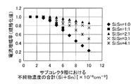
これらのヘテロ接合バイポーラトランジスタについて、サブコレクタ層における不純物濃度の合計と電流増幅率との関係を調査した。
その結果、図3に示すように、置換サイトよりも共有結合半径が小さいn型不純物の不純物濃度(A)と置換サイトよりも共有結合半径が大きいn型不純物の不純物濃度(B)との合計(A)+(B)が3×1018cm-3以上1×1019cm-3以下であり、置換サイトよりも共有結合半径が小さいn型不純物の不純物濃度(A)と置換サイトよりも共有結合半径が大きいn型不純物の不純物濃度(B)との比(A)/(B)が2以上5以下であれば、サブコレクタ層の抵抗を下げつつ、電流増幅率の低下を抑制することができ、本発明の効果を発揮できることが確認された。
また、SiとSn以外の組み合わせであっても、サブコレクタ層の抵抗を下げつつ、電流増幅率の低下を抑制することができ、本発明の効果を発揮できることが確認された。
Claims (6)
- n型GaAsからなるサブコレクタ層を備えるヘテロ接合バイポーラトランジスタ用エピタキシャルウェハにおいて、
前記サブコレクタ層は、置換サイトよりも共有結合半径が小さいn型不純物と置換サイトよりも共有結合半径が大きいn型不純物とを含有していることを特徴とするヘテロ接合バイポーラトランジスタ用エピタキシャルウェハ。 - 前記サブコレクタ層は、置換サイトよりも共有結合半径が小さいn型不純物の不純物濃度(A)と置換サイトよりも共有結合半径が大きいn型不純物の不純物濃度(B)との合計(A)+(B)が3×1018cm-3以上1×1019cm-3以下である請求項1に記載のヘテロ接合バイポーラトランジスタ用エピタキシャルウェハ。
- 前記サブコレクタ層は、置換サイトよりも共有結合半径が小さいn型不純物の不純物濃度(A)と置換サイトよりも共有結合半径が大きいn型不純物の不純物濃度(B)との比(A)/(B)が2以上5以下である請求項1又は2に記載のヘテロ接合バイポーラトランジスタ用エピタキシャルウェハ。
- n型GaAsからなるサブコレクタ層を備えるヘテロ接合バイポーラトランジスタにおいて、
前記サブコレクタ層は、置換サイトよりも共有結合半径が小さいn型不純物と置換サイトよりも共有結合半径が大きいn型不純物とを含有していることを特徴とするヘテロ接合バイポーラトランジスタ。 - 前記サブコレクタ層は、置換サイトよりも共有結合半径が小さいn型不純物の不純物濃度(A)と置換サイトよりも共有結合半径が大きいn型不純物の不純物濃度(B)との合計(A)+(B)が3×1018cm-3以上1×1019cm-3以下である請求項4に記載のヘテロ接合バイポーラトランジスタ。
- 前記サブコレクタ層は、置換サイトよりも共有結合半径が小さいn型不純物の不純物濃度(A)と置換サイトよりも共有結合半径が大きいn型不純物の不純物濃度(B)との比(A)/(B)が2以上5以下である請求項4又は5に記載のヘテロ接合バイポーラトランジスタ。
Priority Applications (1)
| Application Number | Priority Date | Filing Date | Title |
|---|---|---|---|
| US15/561,345 US10312324B2 (en) | 2015-03-26 | 2016-01-12 | Epitaxial wafer for hetero-junction bipolar transistor and hetero-junction bipolar transistor |
Applications Claiming Priority (2)
| Application Number | Priority Date | Filing Date | Title |
|---|---|---|---|
| JP2015064409A JP2016184675A (ja) | 2015-03-26 | 2015-03-26 | ヘテロ接合バイポーラトランジスタ用エピタキシャルウェハ及びヘテロ接合バイポーラトランジスタ |
| JP2015-064409 | 2015-03-26 |
Publications (1)
| Publication Number | Publication Date |
|---|---|
| WO2016152195A1 true WO2016152195A1 (ja) | 2016-09-29 |
Family
ID=56977978
Family Applications (1)
| Application Number | Title | Priority Date | Filing Date |
|---|---|---|---|
| PCT/JP2016/050697 Ceased WO2016152195A1 (ja) | 2015-03-26 | 2016-01-12 | ヘテロ接合バイポーラトランジスタ用エピタキシャルウェハ及びヘテロ接合バイポーラトランジスタ |
Country Status (4)
| Country | Link |
|---|---|
| US (1) | US10312324B2 (ja) |
| JP (1) | JP2016184675A (ja) |
| TW (1) | TW201707090A (ja) |
| WO (1) | WO2016152195A1 (ja) |
Citations (6)
| Publication number | Priority date | Publication date | Assignee | Title |
|---|---|---|---|---|
| JP2000323491A (ja) * | 1999-05-06 | 2000-11-24 | Nec Corp | ヘテロ接合バイポーラトランジスタ及びその製造方法 |
| JP2003303825A (ja) * | 2002-04-05 | 2003-10-24 | Sumitomo Chem Co Ltd | 化合物半導体ウェーハの製造方法、及び化合物半導体素子 |
| JP2004172582A (ja) * | 2002-10-30 | 2004-06-17 | Sharp Corp | ヘテロ接合バイポーラトランジスタ |
| US20070090399A1 (en) * | 2005-10-21 | 2007-04-26 | Yu-Chung Chin | BiFET semiconductor device having vertically integrated FET and HBT |
| US20120326211A1 (en) * | 2011-06-23 | 2012-12-27 | Stevens Kevin S | Bipolar high electron mobility transistor and methods of forming same |
| JP2013021024A (ja) * | 2011-07-07 | 2013-01-31 | Hitachi Cable Ltd | トランジスタ素子 |
Family Cites Families (1)
| Publication number | Priority date | Publication date | Assignee | Title |
|---|---|---|---|---|
| JP2004207548A (ja) | 2002-12-26 | 2004-07-22 | Hitachi Cable Ltd | ヘテロ接合バイポーラトランジスタ用エピタキシャルウェハ及びそれを用いて作製したヘテロ接合バイポーラトランジスタ |
-
2015
- 2015-03-26 JP JP2015064409A patent/JP2016184675A/ja active Pending
-
2016
- 2016-01-12 US US15/561,345 patent/US10312324B2/en active Active
- 2016-01-12 WO PCT/JP2016/050697 patent/WO2016152195A1/ja not_active Ceased
- 2016-01-13 TW TW105100953A patent/TW201707090A/zh unknown
Patent Citations (6)
| Publication number | Priority date | Publication date | Assignee | Title |
|---|---|---|---|---|
| JP2000323491A (ja) * | 1999-05-06 | 2000-11-24 | Nec Corp | ヘテロ接合バイポーラトランジスタ及びその製造方法 |
| JP2003303825A (ja) * | 2002-04-05 | 2003-10-24 | Sumitomo Chem Co Ltd | 化合物半導体ウェーハの製造方法、及び化合物半導体素子 |
| JP2004172582A (ja) * | 2002-10-30 | 2004-06-17 | Sharp Corp | ヘテロ接合バイポーラトランジスタ |
| US20070090399A1 (en) * | 2005-10-21 | 2007-04-26 | Yu-Chung Chin | BiFET semiconductor device having vertically integrated FET and HBT |
| US20120326211A1 (en) * | 2011-06-23 | 2012-12-27 | Stevens Kevin S | Bipolar high electron mobility transistor and methods of forming same |
| JP2013021024A (ja) * | 2011-07-07 | 2013-01-31 | Hitachi Cable Ltd | トランジスタ素子 |
Non-Patent Citations (1)
| Title |
|---|
| OHNO, TAKEO ET AL.: "Sidewall GaAs tunnel junctions fabricated using molecular layer epitaxy", SCIENCE AND TECHNOLOGY OF ADVANCED MATERIALS, vol. 13, no. 1, February 2012 (2012-02-01), pages 013002, XP055315671 * |
Also Published As
| Publication number | Publication date |
|---|---|
| US10312324B2 (en) | 2019-06-04 |
| JP2016184675A (ja) | 2016-10-20 |
| US20180061948A1 (en) | 2018-03-01 |
| TW201707090A (zh) | 2017-02-16 |
Similar Documents
| Publication | Publication Date | Title |
|---|---|---|
| CN102428555B (zh) | 半导体基板、半导体基板的制造方法及电子器件 | |
| JP2003297849A (ja) | ヘテロ接合バイポーラトランジスタ及びその製造方法 | |
| TWI659533B (zh) | 異質接面雙極性電晶體 | |
| US9397204B2 (en) | Heterojunction bipolar transistor with two base layers | |
| JP5108694B2 (ja) | pn接合を有する薄膜結晶ウエハ及びその製造方法 | |
| JP2013021024A (ja) | トランジスタ素子 | |
| WO2016152195A1 (ja) | ヘテロ接合バイポーラトランジスタ用エピタキシャルウェハ及びヘテロ接合バイポーラトランジスタ | |
| JP2012160662A (ja) | トランジスタ用エピタキシャルウェハの製造方法 | |
| JP5487708B2 (ja) | トランジスタ素子用エピタキシャルウェハの製造方法 | |
| JP2007189200A (ja) | トランジスタ用エピタキシャルウエハおよびトランジスタ | |
| WO2015182592A1 (ja) | ヘテロ接合バイポーラトランジスタ用エピタキシャルウェハ及びヘテロ接合バイポーラトランジスタ | |
| CN117012814B (zh) | InP基异质结双极性晶体管的外延结构及其制备方法 | |
| JP2015233089A (ja) | 化合物半導体素子用エピタキシャルウェハ及び化合物半導体素子 | |
| JP6096569B2 (ja) | ヘテロ接合バイポーラトランジスタの製造方法 | |
| JP2007258258A (ja) | 窒化物半導体素子ならびにその構造および作製方法 | |
| JP5543302B2 (ja) | 化合物半導体ウェーハの製造方法及び化合物半導体素子 | |
| WO2016098778A1 (ja) | 半導体トランジスタ用エピタキシャルウェハ及び半導体トランジスタ | |
| JP4695736B2 (ja) | ヘテロ接合バイポーラトランジスタ | |
| JP2007042936A (ja) | Iii−v族化合物半導体エピタキシャルウェハ | |
| JP2012069767A (ja) | Iii−v族化合物半導体エピタキシャルウェハ及びその製造方法 | |
| JP2007103925A (ja) | 半導体装置及びその製造方法 | |
| CN113823556A (zh) | 半导体外延片及其制备方法、微波通讯电晶体 | |
| JP2012234893A (ja) | Iii−v族化合物半導体エピタキシャルウエハ | |
| JP2012138446A (ja) | 高電子移動度トランジスタ用エピタキシャルウェハの製造方法、及び高電子移動度トランジスタ用エピタキシャルウェハ | |
| JP2007194363A (ja) | GaAs基板を用いたInP系半導体装置 |
Legal Events
| Date | Code | Title | Description |
|---|---|---|---|
| 121 | Ep: the epo has been informed by wipo that ep was designated in this application |
Ref document number: 16768098 Country of ref document: EP Kind code of ref document: A1 |
|
| WWE | Wipo information: entry into national phase |
Ref document number: 15561345 Country of ref document: US |
|
| NENP | Non-entry into the national phase |
Ref country code: DE |
|
| 122 | Ep: pct application non-entry in european phase |
Ref document number: 16768098 Country of ref document: EP Kind code of ref document: A1 |