WO2016152089A1 - 高周波スパッタリング装置及びスパッタリング方法 - Google Patents
高周波スパッタリング装置及びスパッタリング方法 Download PDFInfo
- Publication number
- WO2016152089A1 WO2016152089A1 PCT/JP2016/001459 JP2016001459W WO2016152089A1 WO 2016152089 A1 WO2016152089 A1 WO 2016152089A1 JP 2016001459 W JP2016001459 W JP 2016001459W WO 2016152089 A1 WO2016152089 A1 WO 2016152089A1
- Authority
- WO
- WIPO (PCT)
- Prior art keywords
- processing substrate
- movable body
- substrate
- sputtering apparatus
- movable
- Prior art date
- Legal status (The legal status is an assumption and is not a legal conclusion. Google has not performed a legal analysis and makes no representation as to the accuracy of the status listed.)
- Ceased
Links
Images


Classifications
-
- C—CHEMISTRY; METALLURGY
- C23—COATING METALLIC MATERIAL; COATING MATERIAL WITH METALLIC MATERIAL; CHEMICAL SURFACE TREATMENT; DIFFUSION TREATMENT OF METALLIC MATERIAL; COATING BY VACUUM EVAPORATION, BY SPUTTERING, BY ION IMPLANTATION OR BY CHEMICAL VAPOUR DEPOSITION, IN GENERAL; INHIBITING CORROSION OF METALLIC MATERIAL OR INCRUSTATION IN GENERAL
- C23C—COATING METALLIC MATERIAL; COATING MATERIAL WITH METALLIC MATERIAL; SURFACE TREATMENT OF METALLIC MATERIAL BY DIFFUSION INTO THE SURFACE, BY CHEMICAL CONVERSION OR SUBSTITUTION; COATING BY VACUUM EVAPORATION, BY SPUTTERING, BY ION IMPLANTATION OR BY CHEMICAL VAPOUR DEPOSITION, IN GENERAL
- C23C14/00—Coating by vacuum evaporation, by sputtering or by ion implantation of the coating forming material
- C23C14/22—Coating by vacuum evaporation, by sputtering or by ion implantation of the coating forming material characterised by the process of coating
- C23C14/50—Substrate holders
-
- H—ELECTRICITY
- H01—ELECTRIC ELEMENTS
- H01J—ELECTRIC DISCHARGE TUBES OR DISCHARGE LAMPS
- H01J37/00—Discharge tubes with provision for introducing objects or material to be exposed to the discharge, e.g. for the purpose of examination or processing thereof
- H01J37/32—Gas-filled discharge tubes
- H01J37/32431—Constructional details of the reactor
- H01J37/32697—Electrostatic control
-
- C—CHEMISTRY; METALLURGY
- C23—COATING METALLIC MATERIAL; COATING MATERIAL WITH METALLIC MATERIAL; CHEMICAL SURFACE TREATMENT; DIFFUSION TREATMENT OF METALLIC MATERIAL; COATING BY VACUUM EVAPORATION, BY SPUTTERING, BY ION IMPLANTATION OR BY CHEMICAL VAPOUR DEPOSITION, IN GENERAL; INHIBITING CORROSION OF METALLIC MATERIAL OR INCRUSTATION IN GENERAL
- C23C—COATING METALLIC MATERIAL; COATING MATERIAL WITH METALLIC MATERIAL; SURFACE TREATMENT OF METALLIC MATERIAL BY DIFFUSION INTO THE SURFACE, BY CHEMICAL CONVERSION OR SUBSTITUTION; COATING BY VACUUM EVAPORATION, BY SPUTTERING, BY ION IMPLANTATION OR BY CHEMICAL VAPOUR DEPOSITION, IN GENERAL
- C23C14/00—Coating by vacuum evaporation, by sputtering or by ion implantation of the coating forming material
- C23C14/06—Coating by vacuum evaporation, by sputtering or by ion implantation of the coating forming material characterised by the coating material
- C23C14/08—Oxides
- C23C14/081—Oxides of aluminium, magnesium or beryllium
-
- C—CHEMISTRY; METALLURGY
- C23—COATING METALLIC MATERIAL; COATING MATERIAL WITH METALLIC MATERIAL; CHEMICAL SURFACE TREATMENT; DIFFUSION TREATMENT OF METALLIC MATERIAL; COATING BY VACUUM EVAPORATION, BY SPUTTERING, BY ION IMPLANTATION OR BY CHEMICAL VAPOUR DEPOSITION, IN GENERAL; INHIBITING CORROSION OF METALLIC MATERIAL OR INCRUSTATION IN GENERAL
- C23C—COATING METALLIC MATERIAL; COATING MATERIAL WITH METALLIC MATERIAL; SURFACE TREATMENT OF METALLIC MATERIAL BY DIFFUSION INTO THE SURFACE, BY CHEMICAL CONVERSION OR SUBSTITUTION; COATING BY VACUUM EVAPORATION, BY SPUTTERING, BY ION IMPLANTATION OR BY CHEMICAL VAPOUR DEPOSITION, IN GENERAL
- C23C14/00—Coating by vacuum evaporation, by sputtering or by ion implantation of the coating forming material
- C23C14/22—Coating by vacuum evaporation, by sputtering or by ion implantation of the coating forming material characterised by the process of coating
- C23C14/34—Sputtering
- C23C14/3435—Applying energy to the substrate during sputtering
- C23C14/345—Applying energy to the substrate during sputtering using substrate bias
-
- C—CHEMISTRY; METALLURGY
- C23—COATING METALLIC MATERIAL; COATING MATERIAL WITH METALLIC MATERIAL; CHEMICAL SURFACE TREATMENT; DIFFUSION TREATMENT OF METALLIC MATERIAL; COATING BY VACUUM EVAPORATION, BY SPUTTERING, BY ION IMPLANTATION OR BY CHEMICAL VAPOUR DEPOSITION, IN GENERAL; INHIBITING CORROSION OF METALLIC MATERIAL OR INCRUSTATION IN GENERAL
- C23C—COATING METALLIC MATERIAL; COATING MATERIAL WITH METALLIC MATERIAL; SURFACE TREATMENT OF METALLIC MATERIAL BY DIFFUSION INTO THE SURFACE, BY CHEMICAL CONVERSION OR SUBSTITUTION; COATING BY VACUUM EVAPORATION, BY SPUTTERING, BY ION IMPLANTATION OR BY CHEMICAL VAPOUR DEPOSITION, IN GENERAL
- C23C14/00—Coating by vacuum evaporation, by sputtering or by ion implantation of the coating forming material
- C23C14/22—Coating by vacuum evaporation, by sputtering or by ion implantation of the coating forming material characterised by the process of coating
- C23C14/34—Sputtering
- C23C14/35—Sputtering by application of a magnetic field, e.g. magnetron sputtering
-
- C—CHEMISTRY; METALLURGY
- C23—COATING METALLIC MATERIAL; COATING MATERIAL WITH METALLIC MATERIAL; CHEMICAL SURFACE TREATMENT; DIFFUSION TREATMENT OF METALLIC MATERIAL; COATING BY VACUUM EVAPORATION, BY SPUTTERING, BY ION IMPLANTATION OR BY CHEMICAL VAPOUR DEPOSITION, IN GENERAL; INHIBITING CORROSION OF METALLIC MATERIAL OR INCRUSTATION IN GENERAL
- C23C—COATING METALLIC MATERIAL; COATING MATERIAL WITH METALLIC MATERIAL; SURFACE TREATMENT OF METALLIC MATERIAL BY DIFFUSION INTO THE SURFACE, BY CHEMICAL CONVERSION OR SUBSTITUTION; COATING BY VACUUM EVAPORATION, BY SPUTTERING, BY ION IMPLANTATION OR BY CHEMICAL VAPOUR DEPOSITION, IN GENERAL
- C23C14/00—Coating by vacuum evaporation, by sputtering or by ion implantation of the coating forming material
- C23C14/22—Coating by vacuum evaporation, by sputtering or by ion implantation of the coating forming material characterised by the process of coating
- C23C14/52—Means for observation of the coating process
-
- C—CHEMISTRY; METALLURGY
- C23—COATING METALLIC MATERIAL; COATING MATERIAL WITH METALLIC MATERIAL; CHEMICAL SURFACE TREATMENT; DIFFUSION TREATMENT OF METALLIC MATERIAL; COATING BY VACUUM EVAPORATION, BY SPUTTERING, BY ION IMPLANTATION OR BY CHEMICAL VAPOUR DEPOSITION, IN GENERAL; INHIBITING CORROSION OF METALLIC MATERIAL OR INCRUSTATION IN GENERAL
- C23C—COATING METALLIC MATERIAL; COATING MATERIAL WITH METALLIC MATERIAL; SURFACE TREATMENT OF METALLIC MATERIAL BY DIFFUSION INTO THE SURFACE, BY CHEMICAL CONVERSION OR SUBSTITUTION; COATING BY VACUUM EVAPORATION, BY SPUTTERING, BY ION IMPLANTATION OR BY CHEMICAL VAPOUR DEPOSITION, IN GENERAL
- C23C14/00—Coating by vacuum evaporation, by sputtering or by ion implantation of the coating forming material
- C23C14/22—Coating by vacuum evaporation, by sputtering or by ion implantation of the coating forming material characterised by the process of coating
- C23C14/54—Controlling or regulating the coating process
- C23C14/542—Controlling the film thickness or evaporation rate
-
- H—ELECTRICITY
- H01—ELECTRIC ELEMENTS
- H01J—ELECTRIC DISCHARGE TUBES OR DISCHARGE LAMPS
- H01J37/00—Discharge tubes with provision for introducing objects or material to be exposed to the discharge, e.g. for the purpose of examination or processing thereof
- H01J37/32—Gas-filled discharge tubes
- H01J37/32431—Constructional details of the reactor
- H01J37/32715—Workpiece holder
-
- H—ELECTRICITY
- H01—ELECTRIC ELEMENTS
- H01J—ELECTRIC DISCHARGE TUBES OR DISCHARGE LAMPS
- H01J37/00—Discharge tubes with provision for introducing objects or material to be exposed to the discharge, e.g. for the purpose of examination or processing thereof
- H01J37/32—Gas-filled discharge tubes
- H01J37/34—Gas-filled discharge tubes operating with cathodic sputtering
- H01J37/3402—Gas-filled discharge tubes operating with cathodic sputtering using supplementary magnetic fields
- H01J37/3405—Magnetron sputtering
-
- H—ELECTRICITY
- H01—ELECTRIC ELEMENTS
- H01J—ELECTRIC DISCHARGE TUBES OR DISCHARGE LAMPS
- H01J37/00—Discharge tubes with provision for introducing objects or material to be exposed to the discharge, e.g. for the purpose of examination or processing thereof
- H01J37/32—Gas-filled discharge tubes
- H01J37/34—Gas-filled discharge tubes operating with cathodic sputtering
- H01J37/3411—Constructional aspects of the reactor
- H01J37/3414—Targets
- H01J37/3426—Material
-
- H—ELECTRICITY
- H01—ELECTRIC ELEMENTS
- H01J—ELECTRIC DISCHARGE TUBES OR DISCHARGE LAMPS
- H01J37/00—Discharge tubes with provision for introducing objects or material to be exposed to the discharge, e.g. for the purpose of examination or processing thereof
- H01J37/32—Gas-filled discharge tubes
- H01J37/34—Gas-filled discharge tubes operating with cathodic sputtering
- H01J37/3464—Operating strategies
- H01J37/347—Thickness uniformity of coated layers or desired profile of target erosion
-
- H—ELECTRICITY
- H01—ELECTRIC ELEMENTS
- H01J—ELECTRIC DISCHARGE TUBES OR DISCHARGE LAMPS
- H01J37/00—Discharge tubes with provision for introducing objects or material to be exposed to the discharge, e.g. for the purpose of examination or processing thereof
- H01J37/32—Gas-filled discharge tubes
- H01J37/34—Gas-filled discharge tubes operating with cathodic sputtering
- H01J37/3476—Testing and control
-
- H—ELECTRICITY
- H05—ELECTRIC TECHNIQUES NOT OTHERWISE PROVIDED FOR
- H05H—PLASMA TECHNIQUE; PRODUCTION OF ACCELERATED ELECTRICALLY-CHARGED PARTICLES OR OF NEUTRONS; PRODUCTION OR ACCELERATION OF NEUTRAL MOLECULAR OR ATOMIC BEAMS
- H05H1/00—Generating plasma; Handling plasma
- H05H1/24—Generating plasma
- H05H1/46—Generating plasma using applied electromagnetic fields, e.g. high frequency or microwave energy
Definitions
- the present invention relates to a high frequency sputtering apparatus and a sputtering method.
- Patent Document 1 This type of high-frequency sputtering apparatus is known from Patent Document 1, for example.
- This includes a stage that holds a processing substrate in a vacuum chamber in a state where one side of the processing substrate is opened and electrically insulated. Then, a rare gas such as argon gas is introduced into a vacuum chamber evacuated to a predetermined pressure, high frequency power is applied to the target, the target is sputtered, and sputtered particles generated thereby are deposited and deposited on one side of the processing substrate. Then, a predetermined thin film is formed.
- argon gas argon gas
- the high-frequency sputtering apparatus of the present invention that applies high-frequency power to a target in vacuum and forms a film on one side of the processing substrate is open and electrically insulated on one side of the processing substrate.
- a movable body connected to the ground that is movable in the proximity direction or the separation direction with respect to the processing substrate is provided.
- the movable body provided on the stage when the movable body provided on the stage is moved so as to approach from the position separated from the processing substrate, the distance between the other surface of the processing substrate and the movable body is reduced, and the processing substrate and the movable body are reduced. Accordingly, the self-bias potential applied to the processing substrate when sputtering the target by applying high-frequency power can be lowered accordingly. As a result, it is possible to efficiently form a film while suppressing as much as possible the reverse sputtering amount on the processing substrate.
- a circuit having a predetermined or variable impedance between the movable body and the ground.
- a circuit having a variable impedance a matching box capable of adjusting the impedance can be used.
- the movable body has a first movable portion having a facing surface facing a central region of the processing substrate. According to this, by moving the first movable part in the proximity direction or the separation direction with respect to the processing substrate and controlling the distance between the first movable part and the processing substrate, the central region of the processing substrate is obtained. Since the reverse sputtering amount can be controlled by locally changing the applied self-bias potential, it is advantageous when adjusting the in-plane film thickness distribution. In this case, the measurement means for measuring the capacitance between the facing surface and the processing substrate is provided, and if the movement amount of the first movable part is obtained based on the measurement result, the in-plane distribution of the film thickness is adjusted with high accuracy. can do.
- the facing surface includes not only a flat surface but also a curved surface.
- At least one second movable part having a ring-shaped surface of a predetermined area that is concentrically arranged around the first movable part and faces a region excluding the central region of the processing substrate is further provided. It is preferable that both the first and second movable parts are driven by driving means. According to this, the distance between each movable part and the processing substrate is controlled by moving the second movable part in the proximity direction or the separation direction with respect to the processing substrate independently from the first movable part. Therefore, it is advantageous that the in-plane film thickness distribution can be controlled more finely.
- the movable body is moved in the proximity direction or the separation direction with respect to the processing substrate, and the position of the movable body is adjusted, and the position of the movable body is adjusted. Thereafter, a high-frequency power is applied to the target for sputtering, and a film forming step for forming a film by depositing and depositing sputtered particles on one surface of the processing substrate is included.
- the adjusting step includes a step of measuring a capacitance between the facing surface and the processing substrate, and obtaining a moving amount of the movable body based on the measurement result.
- a high-frequency sputtering apparatus according to an embodiment of the present invention will be described by taking as an example a case where a processing substrate W is a silicon substrate and an alumina film as an insulating film is formed on the surface of the silicon substrate. explain.
- SM is a magnetron type sputtering apparatus, and this sputtering apparatus SM includes a vacuum chamber 1 that defines a processing chamber 1a.
- a gas pipe 11 for introducing a sputtering gas which is a rare gas such as argon is connected to the side wall of the vacuum chamber 1.
- a mass flow controller 12 is interposed in the gas pipe 11 and communicates with a gas source (not shown).
- the sputter gas whose flow rate is controlled can be introduced into the processing chamber 1a that is evacuated at a constant pumping speed by the vacuum pumping means P, which will be described later, and the pressure in the processing chamber 1a becomes substantially constant during the film forming process. It is to be retained.
- an exhaust pipe 12 communicating with a vacuum exhaust means P such as a turbo molecular pump or a rotary pump.
- a cathode unit C is attached to the ceiling of the vacuum chamber 1.
- the direction facing the ceiling portion side of the vacuum chamber 1 is referred to as “up” and the direction facing the bottom portion side is described as “down”.
- the cathode unit C includes a target assembly 2 and a magnet unit 3 disposed above the target assembly 2.
- the target assembly 2 includes a target 21 made of aluminum oxide formed into a circular plate shape in plan view according to the contour of the substrate W, and a bonding material (not shown) such as indium on the upper surface of the target 21.
- the backing plate 22 is joined to the base plate 21.
- the target 21 can be cooled by flowing a coolant (cooling water) through the inside of the backing plate 22 during film formation by sputtering. With the target 21 mounted, the peripheral edge of the lower surface of the backing plate 22 is attached to the upper part of the side wall of the vacuum chamber 1 via the insulator I.
- An output from the high frequency power source E is connected to the target 21, and high frequency power is input to the target 21 during the film forming process.
- the magnet unit 3 generates a magnetic field in a lower space below the sputtering surface of the target 21, captures electrons etc. ionized below the sputtering surface during sputtering, and efficiently ionizes the sputtered particles scattered from the target 21. Since it has a structure, detailed description is omitted here.
- a metal stage 4 is disposed at the bottom of the vacuum chamber 1 so as to face the target 21 so that the substrate W is positioned and held in a state where the upper surface, which is the film formation surface, is opened.
- the distance between the target 21 and the substrate W is set in a range of 25 to 80 mm in consideration of productivity, the number of scattering times, and the like.
- the stage 4 may be constituted by a known electrostatic chuck.
- the stage 4 has a recess 42 in the holding surface 41 of the processing substrate W, and the other surface Wb of the processing substrate W when the processing substrate W is held such that the outer peripheral edge of the processing substrate W comes into contact with the holding surface 41.
- a space 43 is defined by the contour of the recess 42.
- a movable body 44 connected to the ground is provided in this space 43.
- a drive shaft 45a of a known drive means 45 is connected to the movable body 44, and the movable body 44 is moved relative to the processing substrate W by driving the drive shaft 45a in the vertical direction using a control means described later. It is configured to move forward and backward.
- a circuit 46 having a predetermined or variable impedance is interposed between the movable body 44 and the ground.
- circuit 46 a known circuit having elements such as a resistor, a coil, and a capacitor (not shown) can be used.
- circuit 46 having a variable impedance a known matching box capable of adjusting the impedance can be used.
- the movable body 44 may be connected to the ground without the circuit 46 (see FIG. 2).
- a known vacuum sealing means such as a vacuum bellows (not shown) is provided.
- the sputtering apparatus SM has known control means including a microcomputer, a sequencer, and the like, and the control means operates the high-frequency power source E, the mass flow controller 12, and the vacuum exhaust means P. The operation of the means 45 is integrated and managed.
- the sputtering method of this embodiment will be described with reference to FIG. 3 as an example in which an aluminum oxide film is formed on the surface of the silicon substrate W using the sputtering apparatus SM.
- the driving unit 45 is driven to move the movable body 44 provided on the stage 4 so as to approach the position away from the processing substrate W to adjust the position of the movable body 44, the other surface Wb of the processing substrate W and The distance g between the movable body 44 is shortened, and the capacitance between the processing substrate W and the movable body 44 is increased (adjustment process).
- the mass flow controller 12 is controlled to introduce argon gas at a predetermined flow rate (for example, 100 sccm) (at this time, the pressure in the processing chamber 1a becomes 1.3 Pa).
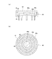
- the first movable portion which is the movable body 44 has an opposing surface 44f facing the central region Rc of the processing substrate W
- the first movable portion 44 is in the proximity direction or the separation direction with respect to the processing substrate W.
- the self-bias potential applied to the central region Rc of the processing substrate W can be locally changed, and the reverse sputtering amount in the central region Rc can be controlled. Can be adjusted.
- the facing surface 44f of the movable body 44 includes not only a flat surface as shown in FIG. 1 but also a curved surface as shown in FIG. If the opposing surface 44f is formed of a curved surface, the reverse sputtering amount can be finely controlled in accordance with the curvature in the central region Rc of the processing substrate W, and consequently the in-plane film thickness distribution can be finely controlled.
- the movable body 44 is concentrically disposed around the first movable portion 44a and has at least a ring-shaped surface having a predetermined area facing the region excluding the central region Rc of the processing substrate W. It further has one (two in the case shown in FIG. 3) second movable parts 44b, 44c, and each of the first and second movable parts 44a, 44b, 44c is driven by a driving means. It is preferable. Since the driving means is known, it is not shown in FIG.
- each movable part 44a, 44b, 44c is moved and each distance between the processing substrates W is controlled, the number of places for adjusting the reverse sputtering amount increases in the radial direction, so that the film is made more finely.
- the distribution in the thickness plane can be controlled.
- the capacitance between each movable portion 44a, 44b, 44c and the portion of the processing substrate W facing it is measured using a measuring means (not shown).
- each driving means is driven according to the obtained amount of movement.
- the distance between each movable part 44a, 44b, 44c and the processing substrate W may be controlled.
- the measuring means obtains the capacitance from the distance to the processing substrate W like a laser displacement meter, or applies an alternating voltage (AC) to a pole to be measured in a state where one pole is in contact with the measuring means. Since a known device such as a device for obtaining a capacitance from a flowing current can be used, detailed description thereof is omitted here.
- the following experiment was performed using the sputtering apparatus SM.
- a silicon substrate having a diameter of 300 mm is used as the processing substrate W, and after setting the processing substrate W on the stage 4 in the vacuum chamber 1, the movable body 44 is moved up to move the other surface Wb of the processing substrate W and the movable body 44. The distance between was adjusted to 0.4 mm.
- Argon gas was introduced into the processing chamber 1a at a flow rate of 100 sccm (the pressure in the processing chamber 1a at this time was about 1.3 Pa), and 600 W of 13.56 MHz high-frequency power was supplied to the stage 4.
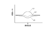
- the in-plane distribution of the film formation rate at this time is 1.27%, and it was found that the in-plane distribution of film thickness can be adjusted by changing the distance between the movable body 44 and the processing substrate W. This is presumably because the self-bias potential applied to the processing substrate W can be adjusted and the reverse sputtering amount can be adjusted. Further, the movable body 44 was further moved up and brought into contact with the processing substrate W (the distance between them was 0.0 mm), and sputtering was performed under the same conditions as described above, and the film formation rate at that time was measured. As shown by line L3 in FIG. 4, it was confirmed that the in-plane distribution of the film formation rate was 1.39%.
- SM high frequency sputtering apparatus
- W processing substrate
- Wa one side of processing substrate W
- Wb other surface of processing substrate W
- Rc central region of processing substrate W
- 4 stage, 41: holding surface
- 42 depression , 43 ... space
Landscapes
- Chemical & Material Sciences (AREA)
- Engineering & Computer Science (AREA)
- Physics & Mathematics (AREA)
- Plasma & Fusion (AREA)
- Analytical Chemistry (AREA)
- Materials Engineering (AREA)
- Chemical Kinetics & Catalysis (AREA)
- Mechanical Engineering (AREA)
- Metallurgy (AREA)
- Organic Chemistry (AREA)
- Electromagnetism (AREA)
- Spectroscopy & Molecular Physics (AREA)
- Physical Vapour Deposition (AREA)
- Plasma Technology (AREA)
Abstract
Description
Claims (7)
- 真空中でターゲットに高周波電力を投入し、処理基板の片面に対し成膜処理を施す高周波スパッタリング装置であって、処理基板の片面を開放しかつ電気的に絶縁した状態で処理基板を保持するステージを備えるものにおいて、
ステージは、その処理基板の保持面に窪み部を有し、処理基板の外周縁部がステージの保持面に当接するように処理基板を保持したときに処理基板他面と窪み部の輪郭とで区画される空間に、処理基板に対して近接方向または離間方向に移動自在なアースに接続される可動体を設けることを特徴とする高周波スパッタリング装置。 - 可動体とアースとの間に、所定の又は可変のインピーダンスを有する回路を介在させることを特徴とする請求項1記載の高周波スパッタリング装置。
- 前記可動体は、処理基板の中央領域に対峙する所定面積の対峙面を持つ第1の可動部分を有することを特徴とする請求項1又は2記載の高周波スパッタリング装置
- 前記対峙面と処理基板との間の静電容量を測定する測定手段を備えることを特徴とする請求項3記載の高周波スパッタリング装置。
- 前記可動体は、前記第1の可動部分の周囲に同心で配置され、処理基板の中央領域を除く領域に対峙する所定面積のリング状面を持つ少なくとも1個の第2の可動部分を更に有し、第1及び第2の両可動部分は夫々が駆動手段で駆動されることを特徴とする請求項3又は4記載の高周波スパッタリング装置。
- 請求項1~5のいずれか1項記載の高周波スパッタリング装置を用いたスパッタリング方法において、
前記可動体を処理基板に対して近接方向または離間方向に移動させて可動体の位置を調整する調整工程と、可動体の位置を調整した後、ターゲットに高周波電力を投入してスパッタリングし、スパッタ粒子を処理基板の片面に付着、堆積させて成膜する成膜工程とを含むことを特徴とするスパッタリング方法。 - 前記調整工程は、前記対峙面と処理基板との間の静電容量を測定する工程を有し、その測定結果に基づき可動体の移動量を求めることを特徴とする請求項6記載のスパッタリング方法。
Priority Applications (5)
| Application Number | Priority Date | Filing Date | Title |
|---|---|---|---|
| SG11201700619UA SG11201700619UA (en) | 2015-03-25 | 2016-03-15 | Rf sputtering apparatus and sputtering method |
| JP2016533669A JP6030813B1 (ja) | 2015-03-25 | 2016-03-15 | 高周波スパッタリング装置及びスパッタリング方法 |
| KR1020177025057A KR101871900B1 (ko) | 2015-03-25 | 2016-03-15 | 고주파 스퍼터링 장치 및 스퍼터링 방법 |
| US15/329,097 US9960018B2 (en) | 2015-03-25 | 2016-03-15 | RF sputtering apparatus and sputtering method |
| CN201680002499.7A CN106795625B (zh) | 2015-03-25 | 2016-03-15 | 高频溅射装置及溅射方法 |
Applications Claiming Priority (2)
| Application Number | Priority Date | Filing Date | Title |
|---|---|---|---|
| JP2015062420 | 2015-03-25 | ||
| JP2015-062420 | 2015-03-25 |
Publications (1)
| Publication Number | Publication Date |
|---|---|
| WO2016152089A1 true WO2016152089A1 (ja) | 2016-09-29 |
Family
ID=56977257
Family Applications (1)
| Application Number | Title | Priority Date | Filing Date |
|---|---|---|---|
| PCT/JP2016/001459 Ceased WO2016152089A1 (ja) | 2015-03-25 | 2016-03-15 | 高周波スパッタリング装置及びスパッタリング方法 |
Country Status (7)
| Country | Link |
|---|---|
| US (1) | US9960018B2 (ja) |
| JP (1) | JP6030813B1 (ja) |
| KR (1) | KR101871900B1 (ja) |
| CN (1) | CN106795625B (ja) |
| SG (1) | SG11201700619UA (ja) |
| TW (1) | TWI673380B (ja) |
| WO (1) | WO2016152089A1 (ja) |
Families Citing this family (4)
| Publication number | Priority date | Publication date | Assignee | Title |
|---|---|---|---|---|
| WO2020066247A1 (ja) * | 2018-09-27 | 2020-04-02 | 株式会社アルバック | マグネトロンスパッタリング装置用の磁石ユニット |
| KR102923867B1 (ko) | 2019-07-09 | 2026-02-04 | 삼성전자주식회사 | 스퍼터링 장치 및 이를 이용한 반도체 장치의 제조 방법 |
| KR102481390B1 (ko) | 2020-10-14 | 2022-12-23 | 부산대학교 산학협력단 | 박막의 원자층 제어를 위한 rf 스퍼터링 장치 |
| TWI908441B (zh) * | 2024-11-05 | 2025-12-11 | 汎銓科技股份有限公司 | 濺鍍設備 |
Citations (3)
| Publication number | Priority date | Publication date | Assignee | Title |
|---|---|---|---|---|
| WO2008108349A1 (ja) * | 2007-03-06 | 2008-09-12 | Shibaura Mechatronics Corporation | プラズマ処理装置 |
| JP2010077452A (ja) * | 2007-10-04 | 2010-04-08 | Canon Anelva Corp | 高周波スパッタリング装置 |
| JP2011068918A (ja) * | 2009-09-24 | 2011-04-07 | Tokyo Electron Ltd | 載置台構造及びプラズマ成膜装置 |
Family Cites Families (10)
| Publication number | Priority date | Publication date | Assignee | Title |
|---|---|---|---|---|
| JPH0791645B2 (ja) * | 1989-04-28 | 1995-10-04 | 株式会社日立製作所 | 薄膜形成装置 |
| WO1992016671A1 (fr) * | 1991-03-20 | 1992-10-01 | Canon Kabushiki Kaisha | Procede et dispositif de formation d'une couche mince par pulverisation |
| JP3565311B2 (ja) * | 1997-12-17 | 2004-09-15 | アルプス電気株式会社 | プラズマ処理装置 |
| TW540284B (en) * | 2001-09-05 | 2003-07-01 | Zeon Corp | Process for manufacturing multi-layer circuit substrate |
| US20060096857A1 (en) * | 2004-11-08 | 2006-05-11 | Ilya Lavitsky | Physical vapor deposition chamber having a rotatable substrate pedestal |
| JP4614220B2 (ja) * | 2004-11-10 | 2011-01-19 | パナソニック株式会社 | スパッタリング装置およびスパッタリング方法 |
| JP5023505B2 (ja) * | 2006-02-09 | 2012-09-12 | 東京エレクトロン株式会社 | 成膜方法、プラズマ成膜装置及び記憶媒体 |
| WO2009044473A1 (ja) | 2007-10-04 | 2009-04-09 | Canon Anelva Corporation | 高周波スパッタリング装置 |
| US8784622B2 (en) * | 2007-12-06 | 2014-07-22 | Intevac, Inc. | System and method for dual-sided sputter etch of substrates |
| JP6007070B2 (ja) | 2012-11-06 | 2016-10-12 | 株式会社アルバック | スパッタリング方法及びスパッタリング装置 |
-
2016
- 2016-03-15 WO PCT/JP2016/001459 patent/WO2016152089A1/ja not_active Ceased
- 2016-03-15 CN CN201680002499.7A patent/CN106795625B/zh active Active
- 2016-03-15 US US15/329,097 patent/US9960018B2/en active Active
- 2016-03-15 JP JP2016533669A patent/JP6030813B1/ja active Active
- 2016-03-15 KR KR1020177025057A patent/KR101871900B1/ko active Active
- 2016-03-15 SG SG11201700619UA patent/SG11201700619UA/en unknown
- 2016-03-22 TW TW105108836A patent/TWI673380B/zh active
Patent Citations (3)
| Publication number | Priority date | Publication date | Assignee | Title |
|---|---|---|---|---|
| WO2008108349A1 (ja) * | 2007-03-06 | 2008-09-12 | Shibaura Mechatronics Corporation | プラズマ処理装置 |
| JP2010077452A (ja) * | 2007-10-04 | 2010-04-08 | Canon Anelva Corp | 高周波スパッタリング装置 |
| JP2011068918A (ja) * | 2009-09-24 | 2011-04-07 | Tokyo Electron Ltd | 載置台構造及びプラズマ成膜装置 |
Also Published As
| Publication number | Publication date |
|---|---|
| TW201708580A (zh) | 2017-03-01 |
| KR20170107092A (ko) | 2017-09-22 |
| US20170213706A1 (en) | 2017-07-27 |
| US9960018B2 (en) | 2018-05-01 |
| JPWO2016152089A1 (ja) | 2017-04-27 |
| SG11201700619UA (en) | 2017-03-30 |
| JP6030813B1 (ja) | 2016-11-24 |
| CN106795625A (zh) | 2017-05-31 |
| CN106795625B (zh) | 2018-05-22 |
| TWI673380B (zh) | 2019-10-01 |
| KR101871900B1 (ko) | 2018-06-27 |
Similar Documents
| Publication | Publication Date | Title |
|---|---|---|
| KR101926677B1 (ko) | 성막 장치 및 성막 방법 | |
| JP7236477B2 (ja) | Pvd装置 | |
| JP6030813B1 (ja) | 高周波スパッタリング装置及びスパッタリング方法 | |
| JP5065725B2 (ja) | プラズマ処理装置 | |
| JP6471000B2 (ja) | マグネトロンスパッタリング装置用の磁石ユニット及びこの磁石ユニットを用いたスパッタリング方法 | |
| JP2013139642A (ja) | スパッタ成膜応用のためのプラズマ処理装置 | |
| JP2002363740A (ja) | スパッタ成膜応用のためのプラズマ処理装置 | |
| CN109154076B (zh) | 成膜方法和溅射装置 | |
| JP2017008374A (ja) | ずれ量の測定方法 | |
| JP6824701B2 (ja) | 成膜方法及び成膜装置 | |
| JP2014148703A (ja) | スパッタリング装置 | |
| KR102330944B1 (ko) | 반응성 이온 에칭 장치 | |
| JP6088780B2 (ja) | プラズマ処理方法及びプラズマ処理装置 | |
| JP5914786B1 (ja) | 絶縁物ターゲット | |
| JP2017139164A (ja) | プラズマ処理装置 | |
| JP6641382B2 (ja) | カーボン膜の成膜方法 | |
| JP2016117923A (ja) | スパッタリング装置 | |
| JP2018135575A (ja) | スパッタリング装置 |
Legal Events
| Date | Code | Title | Description |
|---|---|---|---|
| ENP | Entry into the national phase |
Ref document number: 2016533669 Country of ref document: JP Kind code of ref document: A |
|
| 121 | Ep: the epo has been informed by wipo that ep was designated in this application |
Ref document number: 16767996 Country of ref document: EP Kind code of ref document: A1 |
|
| WWE | Wipo information: entry into national phase |
Ref document number: 15329097 Country of ref document: US |
|
| ENP | Entry into the national phase |
Ref document number: 20177025057 Country of ref document: KR Kind code of ref document: A |
|
| NENP | Non-entry into the national phase |
Ref country code: DE |
|
| 122 | Ep: pct application non-entry in european phase |
Ref document number: 16767996 Country of ref document: EP Kind code of ref document: A1 |