WO2016151773A1 - 発光装置 - Google Patents
発光装置 Download PDFInfo
- Publication number
- WO2016151773A1 WO2016151773A1 PCT/JP2015/058966 JP2015058966W WO2016151773A1 WO 2016151773 A1 WO2016151773 A1 WO 2016151773A1 JP 2015058966 W JP2015058966 W JP 2015058966W WO 2016151773 A1 WO2016151773 A1 WO 2016151773A1
- Authority
- WO
- WIPO (PCT)
- Prior art keywords
- light emitting
- light
- region
- electrode
- layer
- Prior art date
- Legal status (The legal status is an assumption and is not a legal conclusion. Google has not performed a legal analysis and makes no representation as to the accuracy of the status listed.)
- Ceased
Links
Images









Classifications
-
- H—ELECTRICITY
- H05—ELECTRIC TECHNIQUES NOT OTHERWISE PROVIDED FOR
- H05B—ELECTRIC HEATING; ELECTRIC LIGHT SOURCES NOT OTHERWISE PROVIDED FOR; CIRCUIT ARRANGEMENTS FOR ELECTRIC LIGHT SOURCES, IN GENERAL
- H05B33/00—Electroluminescent light sources
- H05B33/12—Light sources with substantially two-dimensional [2D] radiating surfaces
- H05B33/22—Light sources with substantially two-dimensional [2D] radiating surfaces characterised by the chemical or physical composition or the arrangement of auxiliary dielectric or reflective layers
-
- H—ELECTRICITY
- H05—ELECTRIC TECHNIQUES NOT OTHERWISE PROVIDED FOR
- H05B—ELECTRIC HEATING; ELECTRIC LIGHT SOURCES NOT OTHERWISE PROVIDED FOR; CIRCUIT ARRANGEMENTS FOR ELECTRIC LIGHT SOURCES, IN GENERAL
- H05B33/00—Electroluminescent light sources
- H05B33/10—Apparatus or processes specially adapted to the manufacture of electroluminescent light sources
-
- H—ELECTRICITY
- H05—ELECTRIC TECHNIQUES NOT OTHERWISE PROVIDED FOR
- H05B—ELECTRIC HEATING; ELECTRIC LIGHT SOURCES NOT OTHERWISE PROVIDED FOR; CIRCUIT ARRANGEMENTS FOR ELECTRIC LIGHT SOURCES, IN GENERAL
- H05B33/00—Electroluminescent light sources
- H05B33/12—Light sources with substantially two-dimensional [2D] radiating surfaces
- H05B33/14—Light sources with substantially two-dimensional [2D] radiating surfaces characterised by the chemical or physical composition or the arrangement of the electroluminescent material, or by the simultaneous addition of the electroluminescent material in or onto the light source
-
- H—ELECTRICITY
- H05—ELECTRIC TECHNIQUES NOT OTHERWISE PROVIDED FOR
- H05B—ELECTRIC HEATING; ELECTRIC LIGHT SOURCES NOT OTHERWISE PROVIDED FOR; CIRCUIT ARRANGEMENTS FOR ELECTRIC LIGHT SOURCES, IN GENERAL
- H05B33/00—Electroluminescent light sources
- H05B33/12—Light sources with substantially two-dimensional [2D] radiating surfaces
- H05B33/26—Light sources with substantially two-dimensional [2D] radiating surfaces characterised by the composition or arrangement of the conductive material used as an electrode
-
- H—ELECTRICITY
- H10—SEMICONDUCTOR DEVICES; ELECTRIC SOLID-STATE DEVICES NOT OTHERWISE PROVIDED FOR
- H10K—ORGANIC ELECTRIC SOLID-STATE DEVICES
- H10K50/00—Organic light-emitting devices
- H10K50/10—OLEDs or polymer light-emitting diodes [PLED]
- H10K50/11—OLEDs or polymer light-emitting diodes [PLED] characterised by the electroluminescent [EL] layers
- H10K50/125—OLEDs or polymer light-emitting diodes [PLED] characterised by the electroluminescent [EL] layers specially adapted for multicolour light emission, e.g. for emitting white light
-
- H—ELECTRICITY
- H10—SEMICONDUCTOR DEVICES; ELECTRIC SOLID-STATE DEVICES NOT OTHERWISE PROVIDED FOR
- H10K—ORGANIC ELECTRIC SOLID-STATE DEVICES
- H10K50/00—Organic light-emitting devices
- H10K50/80—Constructional details
- H10K50/805—Electrodes
- H10K50/82—Cathodes
- H10K50/828—Transparent cathodes, e.g. comprising thin metal layers
-
- H—ELECTRICITY
- H10—SEMICONDUCTOR DEVICES; ELECTRIC SOLID-STATE DEVICES NOT OTHERWISE PROVIDED FOR
- H10K—ORGANIC ELECTRIC SOLID-STATE DEVICES
- H10K50/00—Organic light-emitting devices
- H10K50/80—Constructional details
- H10K50/86—Arrangements for improving contrast, e.g. preventing reflection of ambient light
- H10K50/865—Arrangements for improving contrast, e.g. preventing reflection of ambient light comprising light absorbing layers, e.g. light-blocking layers
-
- H—ELECTRICITY
- H10—SEMICONDUCTOR DEVICES; ELECTRIC SOLID-STATE DEVICES NOT OTHERWISE PROVIDED FOR
- H10K—ORGANIC ELECTRIC SOLID-STATE DEVICES
- H10K59/00—Integrated devices, or assemblies of multiple devices, comprising at least one organic light-emitting element covered by group H10K50/00
- H10K59/80—Constructional details
- H10K59/8791—Arrangements for improving contrast, e.g. preventing reflection of ambient light
- H10K59/8792—Arrangements for improving contrast, e.g. preventing reflection of ambient light comprising light absorbing layers, e.g. black layers
-
- H—ELECTRICITY
- H10—SEMICONDUCTOR DEVICES; ELECTRIC SOLID-STATE DEVICES NOT OTHERWISE PROVIDED FOR
- H10K—ORGANIC ELECTRIC SOLID-STATE DEVICES
- H10K2101/00—Properties of the organic materials covered by group H10K85/00
- H10K2101/27—Combination of fluorescent and phosphorescent emission
-
- H—ELECTRICITY
- H10—SEMICONDUCTOR DEVICES; ELECTRIC SOLID-STATE DEVICES NOT OTHERWISE PROVIDED FOR
- H10K—ORGANIC ELECTRIC SOLID-STATE DEVICES
- H10K2102/00—Constructional details relating to the organic devices covered by this subclass
- H10K2102/301—Details of OLEDs
- H10K2102/351—Thickness
-
- H—ELECTRICITY
- H10—SEMICONDUCTOR DEVICES; ELECTRIC SOLID-STATE DEVICES NOT OTHERWISE PROVIDED FOR
- H10K—ORGANIC ELECTRIC SOLID-STATE DEVICES
- H10K50/00—Organic light-emitting devices
- H10K50/10—OLEDs or polymer light-emitting diodes [PLED]
- H10K50/17—Carrier injection layers
-
- H—ELECTRICITY
- H10—SEMICONDUCTOR DEVICES; ELECTRIC SOLID-STATE DEVICES NOT OTHERWISE PROVIDED FOR
- H10K—ORGANIC ELECTRIC SOLID-STATE DEVICES
- H10K59/00—Integrated devices, or assemblies of multiple devices, comprising at least one organic light-emitting element covered by group H10K50/00
- H10K59/10—OLED displays
- H10K59/12—Active-matrix OLED [AMOLED] displays
-
- H—ELECTRICITY
- H10—SEMICONDUCTOR DEVICES; ELECTRIC SOLID-STATE DEVICES NOT OTHERWISE PROVIDED FOR
- H10K—ORGANIC ELECTRIC SOLID-STATE DEVICES
- H10K85/00—Organic materials used in the body or electrodes of devices covered by this subclass
- H10K85/30—Coordination compounds
- H10K85/341—Transition metal complexes, e.g. Ru(II)polypyridine complexes
- H10K85/342—Transition metal complexes, e.g. Ru(II)polypyridine complexes comprising iridium
Definitions
- the present invention relates to a light emitting device.
- the organic EL element has a configuration in which an organic layer is sandwiched between a first electrode and a second electrode.
- Examples of light emitting devices having organic EL elements include lighting devices and display devices.
- the light emitting device may be required to make a light emission color of a part of the light emission region different from a light emission color of another part of the light emission region in a light emission region having the same organic layer.
- Patent Document 1 describes that a part of the emission color is made different from that of another region by modifying (degrading) the organic dye in a part of the emission region.
- Patent Document 1 describes a method of irradiating an electromagnetic wave, for example, i-line of a high-pressure mercury lamp, as a method of modifying (degrading) an organic dye.
- Patent Document 2 after the hole injection layer and the hole transport layer are formed and before the light emitting layer is formed, the hole transport layer is irradiated with light from the side opposite to the substrate. Therefore, it is described that the initial luminance reduction can be suppressed.
- the emission color of a part of the light emitting region is different from other parts without reducing the lifetime of the light emitting device.
- the invention according to claim 1 is a substrate; A light emitting part formed on the substrate; With The light emitting unit has a first light emitting region and a second light emitting region, The first light emitting region and the second light emitting region are adjacent to each other, and each includes a first electrode, a second electrode, and an organic layer positioned between the first electrode and the second electrode.
- the invention according to claim 2 is a substrate; A first light emitting region and a second light emitting region formed on the substrate and adjacent to each other; A light limiting layer formed on the substrate and positioned between the first light emitting region and the second light emitting region; With The light limiting layer is a light emitting device including a low transmittance material having a light transmittance lower than that of the material constituting the light limiting layer.
- FIG. 2 is a cross-sectional view taken along the line AA in FIG. It is sectional drawing which shows the structure of an organic layer. It is sectional drawing for demonstrating the manufacturing method of a light-emitting device. It is a figure which shows an example of the light emission spectrum of a 1st light emission area
- FIG. 6 is a plan view showing a configuration of a light emitting device according to Modification Example 1.
- FIG. It is the figure which removed the 2nd electrode from FIG. It is the figure which removed the insulating layer and the organic layer from FIG. 12 is a plan view showing a configuration of a light emitting device according to Modification 2.
- FIG. It is the figure which removed the insulating layer and the organic layer from FIG. It is BB sectional drawing of FIG. It is a figure which shows the modification of FIG.
- FIG. 11 is a cross-sectional view illustrating a configuration of a light emitting device according to Modification 3.
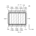
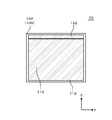
- FIG. 1 is a plan view showing a configuration of a light emitting device 10 according to the embodiment.
- FIG. 2 is a view in which the second electrode 130 is removed from FIG.
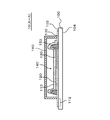
- FIG. 3 is a diagram in which the insulating layer 150 and the organic layer 120 are removed from FIG. 4 is a cross-sectional view taken along the line AA in FIG. In FIG. 1, the sealing portion 160 is omitted for the sake of explanation.
- the light emitting device 10 includes a substrate 100 and a light emitting unit 140.
- the light emitting unit 140 is formed on the substrate 100 and has a first light emitting region 140a and a second light emitting region 140b as shown in FIG.
- the first light emitting region 140a and the second light emitting region 140b are adjacent to each other, and all include the first electrode 110, the organic layer 120, and the second electrode 130.
- the organic layer 120 is located between the first electrode 110 and the second electrode 130.
- the emission spectrum of the first emission region 140a hereinafter referred to as the first emission spectrum
- the emission spectrum of the second emission region 140b hereinafter referred to as the second emission spectrum
- peak intensity ratio The intensity ratio of the second peak to the first peak (hereinafter referred to as peak intensity ratio) is different between the first light emitting region 140a and the second light emitting region 140b.
- the substrate 100 is formed of a material that transmits visible light, such as glass or a light-transmitting resin. However, when the light emitting device 10 is a top emission type, the substrate 100 may be formed of a material that does not have translucency.
- the substrate 100 is, for example, a polygon such as a rectangle.
- the substrate 100 may have flexibility. In the case where the substrate 100 has flexibility, the thickness of the substrate 100 is, for example, not less than 10 ⁇ m and not more than 1000 ⁇ m. In particular, when the substrate 100 is glass, the thickness of the substrate 100 is, for example, 200 ⁇ m or less.
- the substrate 100 is a resin
- the substrate 100 is formed using, for example, PEN (polyethylene naphthalate), PES (polyethersulfone), PET (polyethylene terephthalate), or polyimide.
- PEN polyethylene naphthalate
- PES polyethersulfone
- PET polyethylene terephthalate
- polyimide polyimide
- an inorganic barrier film such as SiN x or SiON is formed on at least the light emitting surface side (preferably both surfaces) of the substrate 100.
- the light emitting unit 140 has an organic EL element.
- This organic EL element has a configuration in which a first electrode 110, an organic layer 120, and a second electrode 130 are laminated in this order on the first surface 102 of the substrate 100.
- the first electrode 110 is a transparent electrode that transmits visible light.
- the transparent conductive material constituting the transparent electrode is a metal-containing material, for example, a metal oxide such as ITO (Indium Tin Oxide), IZO (Indium Zinc Oxide), IWZO (Indium Tungsten Zinc Oxide), ZnO (Zinc Oxide), and the like. is there.
- the thickness of the first electrode 110 is, for example, not less than 10 nm and not more than 500 nm.
- the first electrode 110 is formed using, for example, a sputtering method or a vapor deposition method.
- the first electrode 110 may be a carbon nanotube or a conductive organic material such as PEDOT / PSS.
- the organic layer 120 has a light emitting layer.
- the organic layer 120 has a configuration in which, for example, a hole injection layer, a light emitting layer, and an electron injection layer are stacked.
- the organic layer 120 has a plurality of light emitting layers. Details of the configuration of the organic layer 120 will be described later with reference to FIG.
- the second electrode 130 is made of, for example, a metal selected from the first group consisting of Al, Au, Ag, Pt, Mg, Sn, Zn, and In, or an alloy of a metal selected from the first group. Contains a metal layer.
- the thickness of the second electrode 130 is, for example, not less than 10 nm and not more than 500 nm.
- the second electrode 130 may be formed using the material exemplified as the material of the first electrode 110.
- the second electrode 130 is formed using, for example, a sputtering method or a vapor deposition method.
- the materials of the first electrode 110 and the second electrode 130 described above are examples in the case where light is transmitted through the substrate 100, that is, in the case where light emission of the light emitting device 10 is performed through the substrate 100 (bottom emission type). is there. In other cases, light may pass through the side opposite to the substrate 100. That is, the light emission of the light emitting device 10 is performed without passing through the substrate 100 (top emission type).
- the top emission type includes two types of laminated structures: a reverse product type and a forward product type. In the reverse product type, the material of the first electrode 110 and the material of the second electrode 130 are opposite to those of the bottom emission type.
- the material of the second electrode 130 is used as the material of the first electrode 110, and the material exemplified as the material of the first electrode 110 is selected as the material of the second electrode 130.
- the material of the first electrode 110 is formed on the material of the second electrode 130 described above, the organic layer is further formed thereon, and the second electrode 130 is formed on the organic layer.
- the light emitting device 10 according to the present embodiment may be of any structure of a bottom emission type and the above two types of top emission types.
- the light emitting device 10 has a first terminal 112 and a second terminal 132.
- the first terminal 112 is electrically connected to the first electrode 110.
- the first terminal 112 has a layer formed of the same material as the first electrode 110. Further, this layer may be integrated with the first electrode 110.
- the second terminal 132 is electrically connected to the second electrode 130.
- the second terminal 132 also has a layer formed of the same material as the first electrode 110. However, this layer is separated from the first electrode 110.
- a lead-out wiring may be provided between the first terminal 112 and the first electrode 110.
- a lead wiring may be provided between the second terminal 132 and the second electrode 130.
- a conductive layer made of a material having lower resistance than the first electrode 110 may be formed on the first electrode 110, the first terminal 112, and the second terminal 132.
- This conductive layer is formed of, for example, a metal or an alloy.
- This conductive layer may have a single layer structure or a multilayer structure.
- the conductive layer has a configuration in which, for example, a Mo alloy layer (for example, a MoNb layer), an Al alloy layer (for example, an AlNd layer), and a Mo alloy layer (for example, a MoNb layer) are formed in this order.
- the part located in the 1st electrode 110 among this electrically conductive layer is formed as a some linear electrode, for example.
- a portion of the conductive layer located on the first terminal 112 may be formed on the entire surface of the first terminal 112. Further, a portion of the conductive layer located on the second terminal 132 may be formed on the entire surface of the second terminal 132. By forming this conductive layer, the apparent resistance of the first electrode 110, the first terminal 112, and the second terminal 132 is lowered.
- the light emitting device 10 has an insulating layer 150.
- the insulating layer 150 is provided on the first surface 102 of the substrate 100 to define the light emitting unit 140. In the example illustrated in FIG. 2, the insulating layer 150 covers the edge of the first electrode 110.
- the insulating layer 150 is made of, for example, polyimide, epoxy, acrylic, or novolac resin material.
- the insulating layer 150 is formed, for example, by mixing and applying a photosensitive material to a resin material to be the insulating layer 150, and then exposing and developing the resin material.
- the insulating layer 150 may be formed using an inkjet method or a screen printing method.
- the organic layer 120a is located in the region that becomes the first light emitting region 140a, and the organic layer 120b is located in the region that becomes the second light emitting region 140b.
- the current density is a certain value or less
- the emission color (color temperature) of the organic layer 120a is different from the emission color (color temperature) of the organic layer 120b.
- the difference between the color temperature of the organic layer 120a and the color temperature of the organic layer 120b decreases, and finally there is almost no difference.
- the organic layers 120a and 120b have the same layer structure and are formed using the same process and the same material. For this reason, it is difficult to distinguish between the organic layer 120a and the organic layer 120b in a state where the light emitting device 10 is not emitting light.
- the light emitting unit 140 has one first electrode 110 and one second electrode 130. Therefore, the first electrode 110 of the first light emitting region 140a is electrically and physically connected to the first electrode 110 of the second light emitting region 140b. The second electrode 130 in the first light emitting region 140a is electrically and physically connected to the second electrode 130 in the second light emitting region 140b.
- the light-emitting device 10 has the sealing part 160.
- FIG. The sealing unit 160 seals the light emitting unit 140.
- the sealing portion 160 shown in this figure is a sealing member, and is formed using, for example, a metal such as glass or aluminum, or a resin.
- the sealing portion 160 is a polygon or a circle similar to the substrate 100, and has a shape in which a recess is provided at the center.
- the edge of the sealing portion 160 is fixed to the substrate 100 with an adhesive. Thereby, the space surrounded by the sealing portion 160 and the substrate 100 is sealed. And the light emission part 140 is located in this sealed space.
- the sealing member may be a film formed by an atomic layer deposition (ALD) method or a film formed by a chemical vapor deposition (CVD) method.
- the thickness of the sealing film is, for example, 10 nm or more and 1000 nm or less.
- the sealing film may have, for example, at least one of an aluminum oxide film or a titanium oxide film, or may be a laminated film of these materials.
- the sealing film is formed using a CVD method or a sputtering method, the sealing film is formed of an insulating film such as SiO 2 or SiN.
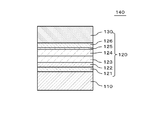
- FIG. 5 is a cross-sectional view showing the configuration of the organic layer 120.
- the organic layer 120 includes a second light-emitting layer 123 and a first light-emitting layer 124 between the hole injection layer 121 and the electron injection layer 126 (or electron transport layer).
- the organic layer 120 includes, from the first electrode 110 side, a hole injection layer 121, a hole transport layer 122, a second light emitting layer 123, a first light emitting layer 124, a hole blocking layer 125, and an electron injection layer. 126 is laminated in this order.
- the hole injection layer 121 is in contact with the first electrode 110
- the electron injection layer 126 is in contact with the second electrode 130.
- the internal emission spectrum of the second light emitting layer 123 has a second peak, and the internal emission spectrum of the first light emitting layer 124 has a first peak.
- the first peak included in the emission spectrum of the output of the light emitting unit 140 (hereinafter referred to as the light emission output spectrum) is derived from the internal emission spectrum from the first light emitting layer 124, and the light emission output spectrum of the light emitting unit 140.
- the second peak contained in is derived from the internal emission spectrum from the second light emitting layer 123.
- the first peak is located, for example, in the blue wavelength range
- the second peak is located, for example, in the red wavelength range.
- first light-emitting layer 124 or the second light-emitting layer 123 may be a single layer and have a plurality of light emission peaks.
- the second light emitting layer 123 has peaks in a red wavelength region and a green wavelength region. Note that at least one of the hole transport layer 122 and the hole block layer 125 may be omitted.
- the light emission output spectrum is indicated by, for example, the result of measuring the light emission of the light emitting unit 140 that is lit from the outside of the light emitting unit 140 using a spectrophotometer.
- the internal emission spectrum is indicated by, for example, a result of measuring the photoluminescence of the light emitting layer to be measured by a microphotoluminescence measuring device.
- the peak wavelengths are common to each other and the peak intensity ratios are different from each other.
- the internal light emission spectrum of the first light emitting region 140a and the internal light emission spectrum of the second light emitting region 140b have the same peak wavelength and peak intensity ratio (almost coincide).
- Each layer constituting the organic layer 120 may be formed by a vapor deposition method. Further, at least one of the organic layers 120, for example, the hole injection layer 121 that is in contact with the first electrode 110 may be formed by a coating method such as an inkjet method, a printing method, or a spray method. In this case, the remaining layers of the organic layer 120 are formed by vapor deposition. Moreover, all the layers of the organic layer 120 may be formed using the apply
- the first light-emitting layer 124 and the second light-emitting layer 123 either a fluorescent light-emitting material or a phosphorescent light-emitting material may be used.
- a phosphorescent material is selected from iridium, platinum, osmium, rhenium, gold, tungsten, ruthenium, hafnium, eurobium, terbium, rhodium, palladium, silver, or the like, and has an atomic weight of 100 to 200.
- a phosphorescent organometallic complex or the like containing one or more atoms is used.
- the first electrode 110 is formed on the first surface 102 of the substrate 100.
- the first terminal 112 and the second terminal 132 are also formed.
- a resin material to be the insulating layer 150 is applied to the first surface 102 of the substrate 100, and this resin material is exposed and developed. Thereby, the insulating layer 150 is formed.
- the organic layer 120 is formed in a region surrounded by the first insulating layer 150 in the first electrode 110.
- the second electrode 130 is formed.
- the sealing part 160 is provided.
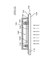
- the organic layer 120 is organically disposed on the second surface 104 side of the substrate 100 through the substrate 100 and the first electrode 110 in a portion of the organic layer 120 that is located in the region that becomes the first light emitting region 140a.
- Light for heating the layer 120 is irradiated.
- This light includes, for example, near-infrared light or infrared light.
- the light intensity is, for example, 1 W or more and 10,000 W or less
- the light irradiation time is, for example, 1 second or more and 36000 seconds or less.
- region 140a among the organic layers 120 is heated, As a result, the light emission output spectrum of the part (organic layer 120a) located in the 1st light emission area
- the peak intensity ratio (ie, “second peak intensity” / “first peak intensity”) is a portion of the organic layer 120 that is not irradiated with light, that is, a portion located in the second light emitting region 140b (organic layer). 120b) is different from the peak intensity ratio of the emission output spectrum.
- the peak intensity ratio of the organic layer 120a is different from the peak intensity ratio of the organic layer 120b because the organic layer 120 is irradiated with light so that the carrier balance of at least one of the second light emitting layer 123 and the first light emitting layer 124 is reached. This is considered to be because the portion where the amount of bonding between holes and electrons is the largest (binding site) moves.
- the light emitting device 10 is the above-described top emission type
- the organic layer 120 is formed from the sealing portion 160 side (the first surface 102 surface side of the substrate 100). The above-mentioned heating light can be irradiated.
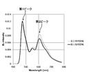
- FIG. 7 is a diagram showing an example of the light emission output spectrum of the first light emission region 140a and the light emission output spectrum of the second light emission region 140b.
- the two light emission output spectra have a plurality of peaks, and the positions of the plurality of peaks, that is, the peak wavelengths are the same.
- the first peak is located in the blue wavelength range
- the second peak is located on the longer wavelength side than the first peak, specifically in the red wavelength range.
- the two emission output spectra have a third peak in the green wavelength region. For this reason, the light emission color of the 1st light emission area
- the first peak becomes strong, the color becomes bluish white (that is, high color temperature), and when the second peak becomes strong, the color becomes reddish white (that is, low color temperature).
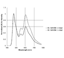
- FIG. 8 shows the emission output spectrum shown in FIG. 7 normalized by the first peak.
- the height of the second peak shown in this figure indicates the above-described peak intensity ratio (second peak / first peak). From this figure, it can be seen that the peak intensity ratio of the first light emitting region 140a is different from the peak intensity ratio of the second light emitting region 140b. In the example shown in the figure, the peak intensity ratio of the second light emitting region 140b is higher than the peak intensity ratio of the first light emitting region 140a. This means that the color temperature of the second light emitting region 140b is lower than the color temperature of the first light emitting region 140a.
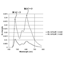
- FIG. 9 is a diagram illustrating how the light emission output spectrum of the first light emitting region 140a varies depending on the magnitude of current (current density).
- FIG. 10 is a graph in which the emission output spectrum shown in FIG. 9 is normalized by the first peak.
- the height of the second peak in FIG. 10 indicates the above-described peak intensity ratio.
- the first light emitting region 140a that is, the region irradiated with light in FIG. 6
- the light becomes stronger as the current density increases as shown in FIG.
- the first current for example, the current density is 5 mA / cm 2 or less
- the first peak is higher than the second peak.
- the first peak is higher than the second peak.
- the difference between the first peak and the second peak is small.
- the peak intensity ratio when the first current flows is different from the peak intensity ratio when the second current flows.
- the current density of the second current is, for example, 101% or more of the current density of the first current.
- FIG. 11 is a diagram showing how the light emission output spectrum of the second light emitting region 140b changes depending on the current magnitude (current density).
- FIG. 12 shows the emission output spectrum shown in FIG. 11 normalized by the first peak. The height of the second peak in FIG. 12 indicates the above-described peak intensity ratio.
- a first current current density is 2.5 mA / cm 2 in the example shown in this figure
- the first peak is higher than the second peak.
- the current density is increased and the second current (in the example shown in the figure, the current density is 10 mA / cm 2 ) is flowing, the first peak is lower than the second peak.
- the difference between the peak intensity ratio of the first light emitting region 140a and the peak intensity ratio of the second light emitting region 140b when the first current is passed is the same as that of the second current. It can be seen that the difference between the peak intensity ratio of the first light emitting region 140a and the peak intensity ratio of the second light emitting region 140b is smaller. This indicates that when the current density is small, the light emission color of the first light emission region 140a and the light emission color of the second light emission region 140b are different, but this difference becomes smaller as the current density is increased. .
- the light emission output spectrum of the light emission part 140 shows the characteristic shown in FIG.9 and FIG.10.
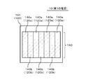
- FIG. 13 is a view of the light emitting device 10 in which the first current flows through the light emitting unit 140, as viewed from the second surface 104 side of the substrate 100 (the surface opposite to the light emitting unit 140).
- the peak intensity ratio of the first light emitting region 140a in this state is different from the peak intensity ratio of the second light emitting region 140b.
- region 140a differs from the light emission color of the 2nd light emission area
- the first light emitting region 140a and the second light emitting region 140b are formed in stripes, but the shape of these light emitting regions is selected as appropriate, such as letters, symbols, pictures, or combinations thereof. May be.
- FIG. 14 is a view of the light emitting device 10 in which the second current flows in the light emitting unit 140 as viewed from the second surface 104 side of the substrate 100.
- the difference between the peak intensity ratio of the first light emitting region 140a and the peak intensity ratio of the second light emitting region 140b in this state is smaller than that when the first current is passed. For this reason, the difference between the emission color of the first emission region 140a and the emission color of the second emission region 140b is smaller than that shown in FIG. 13, and is almost the same depending on the conditions. For this reason, the person cannot distinguish between the first light emitting region 140a and the second light emitting region 140b, and recognizes the light emitting unit 140 as one light emitting region.
- the region corresponding to the first light emitting region 140a can be caused to rise or disappear by changing the current density.
- the display that can be expressed by the difference in emission color between the first light emitting region 140a and the first light emitting region 140a and the second light emitting region 140b may be a character, a symbol, or a picture.
- the shape of the first light emitting region 140a can be freely set by adjusting the light emitting region of the light emitting unit 140.
- the light-off mode the display mode for performing display using the difference in light emission color between the first light-emitting region 140a and the second light-emitting region 140b, the light-emitting mode for performing only light emission with the display turned off, Can be provided with different levels of current values. Therefore, it is not necessary to design the element structure for display or finely adjust the applied current.
- the portion of the organic layer 120 located in the first light emitting region 140a (the organic layer 120a) is heated, and thus the peak of the light emission output spectrum of the first light emitting region 140a of the light emitting unit 140.
- the intensity ratio is different from the peak intensity ratio of the light emission output spectrum of the second light emitting region 140b.
- region 140a can be made different from the light emission color of the 2nd light emission area
- the amount of light applied to the organic layer 120a is small, and the organic dye of the organic layer 120a is not deteriorated. Therefore, it can suppress that the lifetime of the light-emitting device 10 falls.
- the light irradiation to the organic layer 120 a is performed after the light emitting unit 140 is sealed using the sealing unit 160. For this reason, the process of irradiating the organic layer 120a with light can be performed outside the vacuum apparatus. Therefore, an increase in the manufacturing cost of the light emitting device 10 can be suppressed.
- FIG. 15 is a plan view illustrating a configuration of the light emitting device 10 according to the first modification, and corresponds to FIG. 1 of the embodiment.
- FIG. 16 is a diagram in which the second electrode 130 is removed from FIG. 15.
- FIG. 17 is a diagram in which the insulating layer 150 and the organic layer 120 are removed from FIG. 16.
- the light emitting device 10 according to this modification has the same configuration as the light emitting device 10 according to the embodiment except for the following points.
- the insulating layer 150 has a plurality of openings 152 in a region overlapping with the first electrode 110.
- the organic layer 120 is located in each of the plurality of openings 152.
- the light emitting unit 140 is divided into a plurality of light emitting areas.
- the first light emitting areas 140a and the second light emitting areas 140b are alternately arranged.
- the arrangement of the first light emitting region 140a and the second light emitting region 140b is not limited to the example shown in the drawing.
- the second electrode 130 is individually provided for each of the first light emitting region 140a and the second light emitting region 140b.
- the plurality of second electrodes 130 may be connected to the common second terminal 132. Further, the plurality of second electrodes 130 may be connected to different second terminals 132, respectively.
- the applied current to the plurality of second electrodes 130 that is, the first light emitting region 140a and the applied current to the second light emitting region 140b can be individually controlled.
- the emission color of the light emitting device 10 can be adjusted. Such control is performed by the control unit 200 described later.
- the second electrode 130 is formed using, for example, a mask.
- the second electrode 130 may be formed in a predetermined pattern by etching.
- the insulating layer 150 located between the first light emitting region 140a and the second light emitting region 140b is a light limiting layer 154.
- the light limiting layer 154 prevents light incident on the second light emitting region 140b from entering the first light emitting region 140a due to reflection or scattering when the organic layer 120 of the second light emitting region 140b is irradiated with light. It is provided for.
- the light limiting layer 154 may have a near-infrared or infrared light transmittance of 50% or less, and the difference in infrared transmittance between the light limiting layer 154 and other portions is 10% or more. It may be.
- the light limiting layer 154 has a low transmittance with which the resin material constituting the light limiting layer 154 has a lower light transmittance (for example, light in the near infrared region or infrared region) than the resin material. Formed by adding material. In this case, the low-transmittance material is also added to portions of the insulating layer 150 other than the light limiting layer 154.
- the low-transmittance material is, for example, carbon, but may be other materials.
- the light limiting layer 154 of the insulating layer 150 may be formed in a separate process from other portions of the insulating layer 150. In this case, a low transmittance material can be added only to the light limiting layer 154.
- the light limiting layer 154 may include particles or layers that reflect light (for example, metal particles such as Al or metal layers). When providing a metal layer, the resin material of the light limiting layer 154 covers the metal layer.
- the light emission color of the first light emission region 140a can be made different from the light emission color of the second light emission region 140b, as in the embodiment. Moreover, it can suppress that the lifetime of the light-emitting device 10 falls.
- a light limiting layer 154 is formed between the first light emitting region 140a and the second light emitting region 140b.
- the light limiting layer 154 prevents light incident on the second light emitting region 140b from entering the first light emitting region 140a due to reflection or scattering when the organic layer 120 of the second light emitting region 140b is irradiated with light. . Therefore, the boundary between the first light emitting region 140a and the second light emitting region 140b can be clarified, and the width of the first light emitting region 140a can be suppressed from becoming wider than the design value.
- FIG. 18 is a plan view showing the configuration of the light emitting device 10 according to the second modification, and corresponds to FIG. 16 of the first modification.
- FIG. 19 is a diagram in which the insulating layer 150 and the organic layer 120 are removed from FIG. 20 is a cross-sectional view taken along the line BB of FIG. In FIG. 20, the sealing portion 160 is not shown, and the second electrode 130 is shown for explanation.
- the light-emitting device 10 according to this modification has the same configuration as the light-emitting device 10 according to modification 1 except that the first electrode 110 is divided into a plurality of parts. Specifically, the first electrode 110 is provided with one set of the first electrode 110 and the first terminal 112 for one first light emitting region 140a, and one set for one second light emitting region 140b. A pair of first electrodes 110 and first terminals 112 are provided. Therefore, the first electrode 110 in the first light emitting region 140a is separated from the first electrode 110 in the second light emitting region 140b.
- the light limiting layer 154 is located between the adjacent first electrodes 110.
- a current is allowed to flow only in the first light emitting region 140a.
- the insulating layer 150 that does not include a low-transmittance material may be provided between the first light emitting region 140a and the second light emitting region 140b adjacent to each other.
- the second electrodes 130 may be connected to each other as shown in FIG.
- the emission color of the first light emitting area 140a can be made different from the emission color of the second light emitting area 140b. Moreover, it can suppress that the lifetime of the light-emitting device 10 falls. In addition, the boundary between the first light emitting region 140a and the second light emitting region 140b can be clarified, and the width of the first light emitting region 140a can be suppressed from becoming wider than the design value.
- the first electrode 110 is individually provided for each of the plurality of first light emitting regions 140a and the plurality of second light emitting regions 140b. Accordingly, as shown in FIG. 18, a control unit 200 that controls the amount of current supplied to the light emitting unit 140 is provided. Using the control unit 200, the amount of current supplied to the first light emitting region 140a and the second light emitting region 140b are provided. It is possible to individually control the amount of current supplied to the. In this case, the controller 200 can make the emission color of the first light emitting area 140a and the emission color of the second light emitting area 140b different or match each other. Further, the control unit 200 can slightly change the color of the light emitting unit 140. For example, the light emission color of the light emitting unit 140 can be bluish white or reddish. The adjustment of the emission color of the light emitting device 10 by the control unit 200 can be performed not only in two stages but also in multiple stages.
- FIG. 22 is a cross-sectional view illustrating a configuration of the light emitting device 10 according to the third modification, and corresponds to FIG. 20 of the second modification.
- the first electrode 110 included in the first light emitting region 140a and the first electrode 110 included in the second light emitting region 140b adjacent to the first electrode 110 are connected to each other, and the first light emission is performed.
- the configuration is the same as that of the light emitting device 10 according to the modification 2 except that the second electrode 130 included in the region 140a and the second electrode 130 included in the adjacent second light emitting region 140b are connected to each other.
- the light limiting layer 154 shown in Modification 1 is provided in the light emitting device 10 shown in the embodiment.
- the light emission color of the first light emission region 140a can be made different from the light emission color of the second light emission region 140b. Moreover, it can suppress that the lifetime of the light-emitting device 10 falls. In addition, the boundary between the first light emitting region 140a and the second light emitting region 140b can be clarified, and the width of the first light emitting region 140a can be suppressed from becoming wider than the design value.
Landscapes
- Physics & Mathematics (AREA)
- Optics & Photonics (AREA)
- Engineering & Computer Science (AREA)
- Manufacturing & Machinery (AREA)
- Electroluminescent Light Sources (AREA)
Abstract
Description
前記基板に形成された発光部と、
を備え、
前記発光部は、第1発光領域及び第2発光領域を有し、
前記第1発光領域及び前記第2発光領域は、互いに隣り合っており、かつ、いずれも、第1電極、第2電極、及び前記第1電極と前記第2電極の間に位置する有機層を有しており、
前記基板に形成され、前記第1発光領域と前記第2発光領域の間に位置し、前記第2発光領域に入射した光が前記第1発光領域に入射することを抑制する光制限層と、
を備える発光装置である。
前記基板に形成され、互いに隣り合う第1発光領域及び第2発光領域と、
前記基板に形成され、前記第1発光領域と前記第2発光領域の間に位置する光制限層と、
を備え、
前記光制限層は、前記光制限層を構成する材料よりも光の透過率が低い低透過率材料を含んでいる発光装置である。
図15は、変形例1に係る発光装置10の構成を示す平面図であり、実施形態の図1に対応している。図16は、図15から第2電極130を取り除いた図である。図17は、図16から絶縁層150及び有機層120を取り除いた図である。本変形例に係る発光装置10は、以下の点を除いて実施形態に係る発光装置10と同様の構成である。
図18は、変形例2に係る発光装置10の構成を示す平面図であり、変形例1の図16に対応している。図19は、図18から絶縁層150及び有機層120を取り除いた図である。図20は、図18のB-B断面図である。なお、図20において封止部160の図示は省略されており、また、説明のため第2電極130は図示されている。
図22は、変形例3に係る発光装置10の構成を示す断面図であり、変形例2の図20に対応している。本変形例に係る発光装置10は、第1発光領域140aが有する第1電極110と、その隣の第2発光領域140bが有する第1電極110とが互いに繋がっている点、及び、第1発光領域140aが有する第2電極130と、その隣の第2発光領域140bが有する第2電極130とが互いに繋がっている点を除いて、変形例2に係る発光装置10と同様の構成である。言い換えると、本変形例は、実施形態に示した発光装置10に、変形例1に示した光制限層154を設けたものである。
Claims (8)
- 基板と、
前記基板に形成された発光部と、
を備え、
前記発光部は、第1発光領域及び第2発光領域を有し、
前記第1発光領域及び前記第2発光領域は、互いに隣り合っており、かつ、いずれも、第1電極、第2電極、及び前記第1電極と前記第2電極の間に位置する有機層を有しており、
前記基板に形成され、前記第1発光領域と前記第2発光領域の間に位置し、前記第2発光領域に入射した光が前記第1発光領域に入射することを抑制する光制限層と、
を備える発光装置。 - 基板と、
前記基板に形成され、互いに隣り合う第1発光領域及び第2発光領域と、
前記基板に形成され、前記第1発光領域と前記第2発光領域の間に位置する光制限層と、
を備え、
前記光制限層は、前記光制限層を構成する材料よりも光の透過率が低い低透過率材料を含んでいる発光装置。 - 請求項2に記載の発光装置において、
前記低透過率材料はカーボンである発光装置。 - 請求項1~3のいずれか一項に記載の発光装置において、
前記第1発光領域の発光スペクトルである第1発光スペクトル、及び前記第2発光領域の発光スペクトルである第2発光スペクトルは、いずれも第1ピーク及び第2ピークを有しており、かつ、前記第1ピークに対する前記第2ピークの強度比が互いに異なる発光装置。 - 請求項4に記載の発光装置において、
前記有機層は第1発光層及び第2発光層を有している発光装置。 - 請求項5に記載の発光装置において、
前記第1発光層の発光スペクトルは前記第1ピークを有しており、
前記第2発光層の発光スペクトルは前記第2ピークを有している発光装置。 - 請求項1~6のいずれか一項に記載の発光装置において、
前記第1発光領域の前記第1電極は、前記第2発光領域の前記第1電極から分離している発光装置。 - 請求項7に記載の発光装置において、
前記光制限層は、前記第1発光領域の前記第1電極と、前記第2発光領域の前記第1電極との間に位置している発光装置。
Priority Applications (3)
| Application Number | Priority Date | Filing Date | Title |
|---|---|---|---|
| US15/560,442 US20180076408A1 (en) | 2015-03-24 | 2015-03-24 | Light emitting device |
| PCT/JP2015/058966 WO2016151773A1 (ja) | 2015-03-24 | 2015-03-24 | 発光装置 |
| JP2017507227A JPWO2016151773A1 (ja) | 2015-03-24 | 2015-03-24 | 発光装置 |
Applications Claiming Priority (1)
| Application Number | Priority Date | Filing Date | Title |
|---|---|---|---|
| PCT/JP2015/058966 WO2016151773A1 (ja) | 2015-03-24 | 2015-03-24 | 発光装置 |
Publications (1)
| Publication Number | Publication Date |
|---|---|
| WO2016151773A1 true WO2016151773A1 (ja) | 2016-09-29 |
Family
ID=56978719
Family Applications (1)
| Application Number | Title | Priority Date | Filing Date |
|---|---|---|---|
| PCT/JP2015/058966 Ceased WO2016151773A1 (ja) | 2015-03-24 | 2015-03-24 | 発光装置 |
Country Status (3)
| Country | Link |
|---|---|
| US (1) | US20180076408A1 (ja) |
| JP (1) | JPWO2016151773A1 (ja) |
| WO (1) | WO2016151773A1 (ja) |
Citations (5)
| Publication number | Priority date | Publication date | Assignee | Title |
|---|---|---|---|---|
| JP2009289596A (ja) * | 2008-05-29 | 2009-12-10 | Seiko Epson Corp | 発光装置の製造方法、発光装置、表示装置および電子機器 |
| JP2011108395A (ja) * | 2009-11-13 | 2011-06-02 | Hitachi Displays Ltd | 有機発光表示装置 |
| JP2011151011A (ja) * | 2009-12-22 | 2011-08-04 | Seiko Epson Corp | 発光素子、表示装置および電子機器 |
| JP2012212670A (ja) * | 2011-03-23 | 2012-11-01 | Semiconductor Energy Lab Co Ltd | 発光素子および照明装置 |
| JP2013148748A (ja) * | 2012-01-20 | 2013-08-01 | Seiko Epson Corp | 電気光学装置の製造方法 |
Family Cites Families (6)
| Publication number | Priority date | Publication date | Assignee | Title |
|---|---|---|---|---|
| US6661029B1 (en) * | 2000-03-31 | 2003-12-09 | General Electric Company | Color tunable organic electroluminescent light source |
| KR101112534B1 (ko) * | 2005-03-04 | 2012-03-13 | 삼성전자주식회사 | 유기 발광 표시 소자 및 그 제조 방법 |
| JP5105739B2 (ja) * | 2005-11-25 | 2012-12-26 | 株式会社ジャパンディスプレイセントラル | 有機el表示装置及びその製造方法 |
| KR100953655B1 (ko) * | 2008-07-08 | 2010-04-20 | 삼성모바일디스플레이주식회사 | 유기발광 표시장치 |
| JP4775863B2 (ja) * | 2008-09-26 | 2011-09-21 | 東芝モバイルディスプレイ株式会社 | 有機el表示装置及びその製造方法 |
| JP6012495B2 (ja) * | 2013-02-06 | 2016-10-25 | 株式会社カネカ | 有機el発光システム |
-
2015
- 2015-03-24 JP JP2017507227A patent/JPWO2016151773A1/ja active Pending
- 2015-03-24 US US15/560,442 patent/US20180076408A1/en not_active Abandoned
- 2015-03-24 WO PCT/JP2015/058966 patent/WO2016151773A1/ja not_active Ceased
Patent Citations (5)
| Publication number | Priority date | Publication date | Assignee | Title |
|---|---|---|---|---|
| JP2009289596A (ja) * | 2008-05-29 | 2009-12-10 | Seiko Epson Corp | 発光装置の製造方法、発光装置、表示装置および電子機器 |
| JP2011108395A (ja) * | 2009-11-13 | 2011-06-02 | Hitachi Displays Ltd | 有機発光表示装置 |
| JP2011151011A (ja) * | 2009-12-22 | 2011-08-04 | Seiko Epson Corp | 発光素子、表示装置および電子機器 |
| JP2012212670A (ja) * | 2011-03-23 | 2012-11-01 | Semiconductor Energy Lab Co Ltd | 発光素子および照明装置 |
| JP2013148748A (ja) * | 2012-01-20 | 2013-08-01 | Seiko Epson Corp | 電気光学装置の製造方法 |
Also Published As
| Publication number | Publication date |
|---|---|
| US20180076408A1 (en) | 2018-03-15 |
| JPWO2016151773A1 (ja) | 2017-12-21 |
Similar Documents
| Publication | Publication Date | Title |
|---|---|---|
| JP2024051011A (ja) | 発光装置 | |
| JPWO2016042638A1 (ja) | 発光装置 | |
| US8269415B2 (en) | Organic light emitting device, illumination device and liquid crystal display device having high overall aperture ratio | |
| KR20160032405A (ko) | 유기 발광 표시 장치 및 유기 발광 표시 장치 제조 방법 | |
| JP2016062767A (ja) | 発光装置 | |
| WO2016151772A1 (ja) | 発光装置 | |
| JP6522311B2 (ja) | 発光装置 | |
| WO2016151773A1 (ja) | 発光装置 | |
| JP2016181424A (ja) | 発光装置の製造方法 | |
| JP2016181423A (ja) | 発光装置 | |
| JP6661418B2 (ja) | 発光装置 | |
| CN101964354B (zh) | 有机发光装置、照明装置以及液晶显示器 | |
| JP2017147042A (ja) | 発光装置 | |
| JP6457065B2 (ja) | 発光装置 | |
| JP2015162444A (ja) | 発光装置 | |
| JP6450124B2 (ja) | 発光装置 | |
| JP2016062766A (ja) | 発光装置 | |
| JP6644486B2 (ja) | 発光装置 | |
| JP2023091036A (ja) | 発光装置 | |
| WO2017119068A1 (ja) | 発光装置 | |
| JP2018133274A (ja) | 発光装置 | |
| JP2017076467A (ja) | 発光装置 | |
| JP2017216203A (ja) | 発光装置 | |
| JP6528513B2 (ja) | 面発光モジュール | |
| JP2016170963A (ja) | 発光装置 |
Legal Events
| Date | Code | Title | Description |
|---|---|---|---|
| 121 | Ep: the epo has been informed by wipo that ep was designated in this application |
Ref document number: 15886326 Country of ref document: EP Kind code of ref document: A1 |
|
| ENP | Entry into the national phase |
Ref document number: 2017507227 Country of ref document: JP Kind code of ref document: A |
|
| WWE | Wipo information: entry into national phase |
Ref document number: 15560442 Country of ref document: US |
|
| NENP | Non-entry into the national phase |
Ref country code: DE |
|
| 122 | Ep: pct application non-entry in european phase |
Ref document number: 15886326 Country of ref document: EP Kind code of ref document: A1 |