WO2016139848A1 - Au-Sn-Ag系はんだペースト並びにこのAu-Sn-Ag系はんだペーストを用いて接合もしくは封止された電子部品 - Google Patents
Au-Sn-Ag系はんだペースト並びにこのAu-Sn-Ag系はんだペーストを用いて接合もしくは封止された電子部品 Download PDFInfo
- Publication number
- WO2016139848A1 WO2016139848A1 PCT/JP2015/082578 JP2015082578W WO2016139848A1 WO 2016139848 A1 WO2016139848 A1 WO 2016139848A1 JP 2015082578 W JP2015082578 W JP 2015082578W WO 2016139848 A1 WO2016139848 A1 WO 2016139848A1
- Authority
- WO
- WIPO (PCT)
- Prior art keywords
- solder
- mass
- alloy
- solder paste
- solder alloy
- Prior art date
- Legal status (The legal status is an assumption and is not a legal conclusion. Google has not performed a legal analysis and makes no representation as to the accuracy of the status listed.)
- Ceased
Links
Images




Classifications
-
- B—PERFORMING OPERATIONS; TRANSPORTING
- B23—MACHINE TOOLS; METAL-WORKING NOT OTHERWISE PROVIDED FOR
- B23K—SOLDERING OR UNSOLDERING; WELDING; CLADDING OR PLATING BY SOLDERING OR WELDING; CUTTING BY APPLYING HEAT LOCALLY, e.g. FLAME CUTTING; WORKING BY LASER BEAM
- B23K35/00—Rods, electrodes, materials, or media, for use in soldering, welding, or cutting
- B23K35/22—Rods, electrodes, materials, or media, for use in soldering, welding, or cutting characterised by the composition or nature of the material
- B23K35/24—Selection of soldering or welding materials proper
- B23K35/30—Selection of soldering or welding materials proper with the principal constituent melting at less than 1550°C
-
- C—CHEMISTRY; METALLURGY
- C22—METALLURGY; FERROUS OR NON-FERROUS ALLOYS; TREATMENT OF ALLOYS OR NON-FERROUS METALS
- C22C—ALLOYS
- C22C5/00—Alloys based on noble metals
- C22C5/02—Alloys based on gold
-
- H—ELECTRICITY
- H10—SEMICONDUCTOR DEVICES; ELECTRIC SOLID-STATE DEVICES NOT OTHERWISE PROVIDED FOR
- H10W—GENERIC PACKAGES, INTERCONNECTIONS, CONNECTORS OR OTHER CONSTRUCTIONAL DETAILS OF DEVICES COVERED BY CLASS H10
- H10W72/00—Interconnections or connectors in packages
- H10W72/071—Connecting or disconnecting
-
- H—ELECTRICITY
- H05—ELECTRIC TECHNIQUES NOT OTHERWISE PROVIDED FOR
- H05K—PRINTED CIRCUITS; CASINGS OR CONSTRUCTIONAL DETAILS OF ELECTRIC APPARATUS; MANUFACTURE OF ASSEMBLAGES OF ELECTRICAL COMPONENTS
- H05K3/00—Apparatus or processes for manufacturing printed circuits
- H05K3/30—Assembling printed circuits with electric components, e.g. with resistors
- H05K3/32—Assembling printed circuits with electric components, e.g. with resistors electrically connecting electric components or wires to printed circuits
- H05K3/34—Assembling printed circuits with electric components, e.g. with resistors electrically connecting electric components or wires to printed circuits by soldering
Definitions
- the present invention relates to a high-temperature Pb-free solder paste.
- Au—Sn—Ag solder paste obtained by mixing an Au—Sn—Ag solder alloy mainly composed of Au suitable for high temperature and flux, and an electron bonded or sealed using the solder paste Regarding parts.
- solder materials used for the purpose of joining electronic components to the board.
- Lead has been used as a main component in solder materials for a long time, but it has already been a regulated substance under the Rohs Directive. For this reason, development of a solder material not containing lead (Pb) (hereinafter referred to as a lead-free solder material or a lead-free solder material) has been actively conducted.
- Solder materials used when bonding electronic components to a substrate are roughly classified into high temperature (about 260 ° C. to 400 ° C.) and medium and low temperature (about 140 ° C. to 230 ° C.) depending on the limit temperature of use.
- the medium-low temperature solder material is mainly composed of Sn, and is lead-free.
- Patent Document 1 discloses that “Sn is a main component, Ag is 1.0 to 4.0 wt%, Cu is 2.0 wt% or less, Ni is 1.0 wt% or less, and P is 0.2 wt%. % Of lead-free solder alloy composition ".
- Patent Document 2 describes “Lead-free solder having an alloy composition containing 0.5 to 3.5% by weight of Ag and 0.5 to 2.0% by weight of Cu with the balance being Sn”. .
- Patent Document 3 discloses “Bi / Ag brazing material containing 30 to 80 at% Bi and having a melting temperature of 350 to 500 ° C.”.
- Patent Document 4 discloses "a solder alloy in which a binary eutectic alloy is added to a Bi-containing eutectic alloy and an additional element is further added". Although this solder alloy is a quaternary or higher multi-component solder alloy, it has been shown that the liquidus temperature can be adjusted and variations can be reduced.
- an Au—Sn alloy, an Au—Ge alloy, or the like has already been used in a crystal device, a SAW filter, a MEMS, or the like.
- Au-20% by mass Sn (meaning composed of 80% by mass of Au and 20% by mass of Sn. The same applies hereinafter) is a composition of eutectic point, and its melting point is 280 ° C.
- Au-12.5 mass% Ge has a composition of eutectic point and its melting point is 356 ° C.
- Au-Sn alloy and Au-Ge alloy depends on the difference in melting point. In other words, an Au—Sn alloy is used for bonding at a relatively low temperature even for high temperatures. When the temperature is relatively high, an Au—Ge alloy is used. Furthermore, Au-based solder alloys are very hard compared to Pb-based solder alloys and Sn-based solder alloys. In particular, an Au—Ge alloy is very difficult to process into a sheet shape or the like because Ge is a metalloid. Therefore, productivity and yield are poor, causing cost increase.
- Au—Sn alloy Even if the Au—Sn alloy is not as good as the Au—Ge alloy, it is difficult to process, and the productivity and yield at the time of processing into a preform material are poor. That is, Au-20% by mass Sn is composed of an intermetallic compound even though it has a eutectic point composition. Therefore, dislocations are difficult to move, and therefore, are difficult to deform, and cracks and burrs are likely to occur when thinly rolled or punched with a press.
- Au—Sn alloys are widely used for encapsulating quartz devices that require particularly high reliability by utilizing the melting point and workability.
- the following Au-based solder alloy has been developed.
- Patent Document 6 discloses “a high-temperature lead-free solder alloy for fusion sealing characterized by comprising 2 to 12% by mass of Ag, 40 to 55% by mass of Au, and the remaining Sn”.
- the purpose of this document is to provide a lead-free high-temperature solder that not only requires a smaller amount of Au than the conventional Au—Sn eutectic alloy but also has a solidus temperature of 270 ° C. or higher.
- Another object is to “provide a package in which the joint between the container body and the lid member has excellent heat cycle resistance and mechanical strength”.
- Patent Document 7 states that “a brazing material in which 20 to 50 wt% Au and 10 to 20 wt% Ge or 20 to 40 wt% Sn is added to Ag is attached to the tip of a lead frame pin.
- a “brazed lead frame” is shown. This document states that “a brazing material with a brazing material having a low melting point, does not embrittle the lead frame of Fe—Ni alloy, stabilizes the bonding strength with an appropriate brazing flow, and does not lower the corrosion resistance of the lead frame. The purpose is to provide a lead frame.
- Patent Document 8 discloses that “(A) an Au—Sn mixed powder containing 55 to 70 parts by mass of Sn with respect to a total of 100 parts by mass of Au and Sn, and (B) a flux, Component (A) is (A1) an Au—Sn alloy solder powder containing 18 to 23.5 parts by mass of Sn with respect to 100 parts by mass of Au and Sn, and (A2) a total of 100 of Au and Sn.
- An Au—Sn alloy solder paste characterized by containing an Au—Sn alloy solder powder containing Sn in an amount of 88 to 92 parts by mass with respect to parts by mass is shown. This document states that “Au—Sn alloy solder paste that can be bonded at a low temperature of 280 ° C.
- Au—Sn alloy solder formed by this paste is also used during the second reflow with Sn—Ag lead-free solder. It is intended to provide an Au—Sn alloy solder paste that can be bonded easily to an LED element and that does not melt during the second reflow process, and can reduce material costs by reducing Au. .
- Au—Sn solder material and Au—Ge solder material that have been put into practical use are used for soldering in places that require particularly high reliability, such as crystal devices, SAW filters, and MEMS.
- Au-based solder materials use a large amount of very expensive Au, they are very expensive compared to general-purpose Pb-based solder materials and Sn-based solder materials, and are widely used in general. Is hard to say.
- Au-based solder alloys are very hard and difficult to process. For this reason, for example, it takes time when rolling into a sheet shape, or a special material that does not easily wrinkle the roll must be used, which increases costs.
- Patent Document 5 states that a brazing material and a piezoelectric device that are relatively low melting point, easy to handle, excellent in strength and adhesion, and inexpensive are provided. Furthermore, it is also stated that by limiting the composition ranges of Au, Sn, and Ag, it is possible to obtain the same characteristics as a sealing material while reducing the Au content as compared with the conventional one. .
- Patent Document 5 shows a composition ratio (Au (wt%), Ag (wt%), Sn (wt%)) in a ternary composition diagram of Au, Ag, and Sn.
- Point A1 (41.8, 7.6, 50.5)
- Point A2 (62.6, 3.4, 34.0)
- Point A3 (75.7, 3.2, 21.1)
- Point A4 (53.6, 22.1, 24.3)
- Point A5 (30.3, 33.2, 36.6)
- this region is too high, and it is logically impossible to obtain the desired characteristics in the same manner in all regions of such a wide composition range.
- the point A3 and the point A5 have different Au contents by 45.4% by mass. Although there is a large difference in the Au content in this way, it is unlikely that similar characteristics can be obtained at the points A3 and A5.
- the composition ratio of Au, Sn, and Ag is different, the intermetallic compound produced is different, and the liquidus temperature and the solidus temperature are also greatly different.
- the Au content which is most difficult to oxidize, is different by 45.4% by mass, the wettability also changes greatly.
- the types and amounts of intermetallic compounds produced at the time of joining differ greatly, and it is not possible to achieve the same excellent characteristics with respect to workability and stress relaxation properties in a wide range as shown in Patent Document 5.
- the crystal grains are coarse, the difference between the liquidus temperature and the solidus temperature is large, and a melting phenomenon occurs at the time of joining, so that sufficient joining reliability is achieved. It is difficult to get.
- the brazing material described in Patent Document 7 has a maximum Au content of 50% by mass, and the effect of reducing the Au raw material is very large. Since the Sn content is also 40% by mass or less (or less than 40% by mass), there is a possibility that a certain degree of wettability can be secured.
- the present invention prevents the lead frame made of Fe—Ni alloy from becoming brittle, stabilizes the bonding strength with an appropriate brazing flow, and does not reduce the corrosion resistance of the lead frame. Is the purpose.
- the brazing material disclosed in Patent Document 7 invented from such a viewpoint is unlikely to satisfy the characteristics required for bonding of semiconductor elements, such as stress relaxation due to expansion and contraction due to heat.
- Patent Document 8 describes a low Au, low cost Au—Sn solder paste.
- cost reduction is an important issue for Au-based solder materials, and meeting this market demand is very important for technological progress.
- Patent Document 8 states that “the mechanism by which an Au—Sn alloy solder paste containing the component (A1) and the component (A2) of the present invention joins a semiconductor element such as an LED to a substrate is not clear, but at 260 to 280 ° C. First, the component (A2) is melted by heating to wet an adherend such as a semiconductor element such as an LED or a substrate, and then diffusion between the melted component (A2) and the component (A1) It is considered that an Au—Sn alloy solder in which the component (A2) and the component (A1) are mixed is formed, and this mechanism enables bonding by heating at 280 ° C. or less, which is easy for the LED element, and is solid after the bonding.
- the present invention has been made in view of the above-mentioned problems, and is a high-temperature Au—Sn— excellent in various characteristics that can be sufficiently used even in bonding that requires extremely high reliability, such as a crystal device, a SAW filter, and a MEMS.
- An object of the present invention is to provide an Ag-based solder paste, in particular, a Pb-free solder paste having good wettability at low cost and excellent in workability, stress relaxation property, bonding reliability, and the like.
- the Pb-free Au—Sn—Ag solder paste according to the present invention is obtained by mixing a solder alloy powder and a flux, and when the total amount of the solder alloy powder is 100% by mass, Sn is contained at 27.5 mass% or more and less than 33.0 mass%, Ag is contained at 8.0 mass% or more and 14.5 mass% or less, and the balance is made of Au except for elements inevitably included in production. It is characterized by that.
- the Pb-free Au—Sn—Ag solder paste according to the present invention is characterized in that the flux contains rosin.
- the Pb-free Au—Sn—Ag solder paste according to the present invention contains 29.0% by mass to 32.0% by mass of Sn and 10.0% by mass to 14.0% by mass of Ag. The remainder is made of Au except for elements inevitably included in production.
- the Pb-free Au—Sn—Ag solder paste according to the present invention is characterized in that at least a part of the metal structure of the solder alloy powder is a lamellar structure.
- the Pb-free Au—Sn—Ag solder paste according to the present invention is characterized in that the metal structure of the solder alloy powder is a lamellar structure, and the ratio thereof is 90% by volume or more.
- the present invention also provides a Si semiconductor element bonded body characterized by being bonded using the Pb-free Au—Sn—Ag solder paste.
- the present invention also provides a crystal resonator sealing element characterized by being sealed using the Pb-free Au—Sn—Ag solder paste.
- solder material used in a place requiring extremely high reliability such as a quartz device, a SAW filter, and a MEMS at a lower cost than a conventional Au-based solder material.
- the solder alloy powder of the present invention is based on a eutectic metal, so that the metal structure is a fine lamellar structure, and has excellent flexibility, excellent stress relaxation and bonding reliability, and is mixed with flux.
- an Au-based solder paste having excellent wettability and bondability can be provided by using the solder paste. Therefore, the industrial contribution is extremely high.
- the inventor of the present invention in a solder paste formed by mixing an Au—Sn—Ag solder alloy powder based on the vicinity of the composition of the ternary eutectic point of Au, Sn, and Ag and a flux, When the predetermined solder alloy composition range is satisfied, it has been found that the following properties and effects are obtained, and the present invention has been achieved.
- it is softer than Au-Sn alloy, excellent in workability and stress relaxation, and by replacing a part of expensive Au with Sn and Ag, the Au content is greatly reduced, and the cost of the solder alloy is reduced. It is possible to obtain an Au-based alloy powder having a reduced A.
- the degree of freedom in shape is increased, and a bonding material having excellent wet spreading properties, bonding reliability, and the like is obtained.
- the solder alloy powder and flux in the Au—Sn—Ag solder paste of the present invention will be described in detail.
- the composition of the Au—Sn—Ag solder alloy of the present invention contains Sn of 27.5% by mass or more and less than 33.0% by mass, and Ag is contained by 8.0% by mass or more and 14.5% by mass or less. The remainder is composed of Au except for elements inevitably included in the production.
- the solder alloy of the present invention contains Ag, which is a soft metal in order to reduce the cost of the Au-based solder alloy, which is very expensive, and to have excellent workability and stress relaxation properties, and also to form a ternary eutectic crystal.
- the crystal structure becomes a lamellar structure, workability, stress relaxation properties, etc.
- Au is a main component of the solder alloy used in the present invention, and is naturally an essential element. Since Au is very difficult to oxidize, it is most suitable in terms of characteristics as a component of a solder material for joining and sealing of electronic parts that require high reliability. For this reason, Au-based solder materials are frequently used for sealing quartz devices and SAW filters.
- the solder alloy used in the present invention is also based on Au, and provides a solder material belonging to a technical field that requires such high reliability.
- Au is a very expensive metal, it is better not to use it from the viewpoint of cost. For this reason, it is rarely used for electronic components that require a general level of reliability.
- the solder alloy used in the present invention is equivalent to or better than Au-20 mass% Sn solder alloy or Au-12.5 mass% Ge solder alloy in terms of characteristics such as wettability and bondability.
- an alloy near the composition of the ternary eutectic point of the Au—Sn—Ag system is used.
- ⁇ Sn> Sn is an essential element in the solder alloy used in the present invention, and is a basic element.
- the Au—Sn solder alloy is usually used with a composition near the eutectic point, that is, a composition near Au-20 mass% Sn.
- the solidus temperature becomes 280 ° C.
- the crystal becomes finer, and relatively flexibility is obtained.
- the Au-20 mass% Sn alloy is composed of Au 1 Sn 1 intermetallic compound and Au 5 Sn 1 intermetallic compound, and is hard and brittle. For this reason, it is hard to process, for example, when processing into a sheet form by rolling, it can be made thin only little by little.
- the solder alloy used in the present invention is excellent in workability, stress relaxation properties, etc. It is.
- the melting point can be lowered, and the eutectic point temperature is 370 ° C. which is not significantly different from the eutectic point temperature of the Au—Ge alloy. Having an appropriate melting point as such a high temperature solder alloy is one of the excellent points of the solder alloy used in the present invention.
- the Sn content is 27.5% by mass or more and less than 33.0% by mass.
- the crystal grains become large, and effects such as improvement in flexibility and workability are not sufficiently exhibited.
- the difference between the liquidus temperature and the solidus temperature becomes too large, causing a melting phenomenon.
- the Au content tends to increase, the cost reduction effect is also limited.
- the Sn content is 33.0% by mass or more, there is a problem that the composition of the eutectic point is deviated too much, and the coarsening of the crystal grains and the difference between the liquidus temperature and the solidus temperature increase. Arise.
- the Sn content is excessively large, the Au—Sn—Ag alloy becomes easy to oxidize, and the good wettability characteristic of the Au-based solder material is lost, thereby obtaining high joint reliability. Becomes difficult. If the Sn content is 29.0% by mass or more and 32.0% by mass or less, it is preferable that the composition of the eutectic point is further obtained, the effect of refining crystal grains is obtained, and the melting phenomenon is hardly caused.
- ⁇ Ag> Ag is an essential element in the solder alloy used in the present invention, and is an indispensable element for obtaining a ternary eutectic alloy.
- a composition in the vicinity of the ternary eutectic point of Au—Sn—Ag excellent flexibility, workability, stress relaxation, suitable melting point, and the like can be obtained for the first time. Further, the Au content can be greatly reduced, and thus a large cost reduction can be realized.
- Addition of Ag also has an effect of improving wettability. That is, by adding Ag, the reactivity between the Au—Sn—Ag alloy and Cu, Ni or the like used on the uppermost surface of the substrate or the like is improved, and wettability can be improved.
- content of Ag which exhibits the outstanding effect is 8.0 to 14.5 mass%. If the Ag content is less than 8.0% by mass, the composition of the eutectic point is excessively deviated, the liquidus temperature becomes too high, or the crystal grains become coarse, and a good bond can be obtained. It becomes difficult. On the other hand, even when the Ag content exceeds 14.5% by mass, the liquidus temperature becomes high, causing a phenomenon of dissolution and crystal grain coarsening. If the content of Ag is 10.0% by mass or more and 14.0% by mass or less, it is close to the composition of the eutectic point, and the effect of containing Ag is even more preferable.
- At least a part of the metal structure of the Au—Sn—Ag solder alloy is a lamellar structure, and the ratio thereof is 90% by volume or more.
- a lamellar structure refers to a metal structure in which the stripe interval of a striped structure is 0.1 ⁇ m or more and 2.0 ⁇ m or less.
- a portion surrounded by a square in FIG. 2 is a lamellar tissue defined by the present invention.
- the type of flux used in the solder paste of the present invention is not particularly limited, and for example, a resin system, an inorganic chloride system, an organic halide system, or the like may be used.
- a resin system an inorganic chloride system, an organic halide system, or the like may be used.
- the most common flux that is, a rosin used as a base material and an activator and a solvent added thereto will be described.
- the base material is 20-30% by mass of rosin
- the active agent is 0.2-1% by mass
- the solvent is about 70-80% by mass. It is preferable to blend as described above. Thereby, a solder paste having good wettability and bondability can be obtained. Moreover, if a thixotropic agent is contained to adjust the thixotropy, a solder paste that is even easier to use can be obtained.
- rosin As the base material, natural unmodified rosin such as wood resin rosin, gum rosin and tall oil rosin may be used, or modified rosin ester, hydrogenated rosin, rosin modified resin, polymerized rosin and the like. Rosin may be used.
- Solvents include acetone, amylbenzene, n-amine alcohol, benzene, carbon tetrachloride, methyl alcohol, ethyl alcohol, isopropyl alcohol, n-butanol, isobutyl alcohol, methyl ethyl ketone, toluene, turpentine oil, xylene, cyclohexane, ethylene glycol mono Phenyl ether, ethylene glycol monobutyl ether, carbon tetrachloride, trichloroethane, alkanediol, alkylene glycol, butadiol, triethylene glycol, tetraethylene glycol, tetradecane and the like can be used.
- Activators include phosphoric acid, sodium chloride, ammonium chloride, zinc chloride, stannous chloride, aniline hydrochloride, hydrazine hydrochloride, cetylpyridine bromide, phenylhydrazine hydrochloride, tetrachloronaphthalene, methyl hydrazine hydrochloride, methyl Amine hydrochloride, ethylamine hydrochloride, diethylamine hydrochloride, butylamine hydrochloride, benzoic acid, stearic acid, lactic acid, citric acid, oxalic acid, succinic acid, adipic acid, hivacic acid, triethanolamine, diphenylguanidine, diphenylguanidine HBr, It is possible to use erythritol, xylitolitol, sorbitol, ribitol and the like.
- a thixotropic agent is contained to adjust the thixotropy, a solder paste that is even easier to use can be obtained.
- a thixotropic agent for example, stearic acid amide, oleic acid amide, erucic acid amide can be used.
- a suitable flux can be obtained by selecting a substance suitable for the purpose from these solvents and activators, and adjusting the amount of addition as appropriate. For example, when the oxide film on the joint surface of a solder alloy or a substrate is strong, it is preferable to add a large amount of rosin or activator and adjust the viscosity and fluidity with a solvent.
- solder paste obtained by mixing the solder alloy and the flux has very good wettability due to the action of the flux.
- the solder alloy does not need to be processed into a sheet shape that is difficult to process, and can be used in a powder form that is easy to process.
- the high-temperature Pb-free solder paste of the present invention for joining an electronic component and a substrate, even when used under harsh conditions such as an environment in which a heat cycle is repeated, durability is ensured.
- a highly reliable electronic component substrate can be provided. Therefore, by mounting this electronic component board on, for example, power semiconductor devices such as thyristors and inverters, various control devices mounted in automobiles, devices used under harsh conditions such as solar cells, The reliability of various devices can be further increased.
- the excellent solder paste according to the present invention is also very suitable for sealing a crystal resonator, and can be used, for example, for sealing a crystal resonator package as shown in FIG.
- the crucible containing the raw material was placed in a high-frequency melting furnace, and nitrogen was flowed at a flow rate of 0.7 L / min or more per 1 kg of the raw material in order to suppress oxidation.
- the melting furnace was turned on to heat and melt the raw material.
- the metal began to melt, it was stirred well with a mixing rod and mixed uniformly so as not to cause local compositional variations.
- the high frequency power supply was turned off, the crucible was quickly removed, and the molten metal in the crucible was poured into the solder mother alloy mold.
- a cylindrical mold having an inner diameter of 140 mm was used for atomization in a gas phase for producing powder.
- solder mother alloys of Samples 1 to 16 were produced in the same manner as described above except that the mixing ratio of the raw materials was changed.
- the solder mother alloys of Samples 1 to 16 were subjected to composition analysis using an ICP emission spectroscopic analyzer (SHIMAZU S-8100). The analysis results obtained are shown in Table 1 below.
- the manufacturing method of the alloy powder for solder paste is not particularly limited, it is generally manufactured by an atomizing method.
- the atomization method may be performed in the gas phase or in the liquid phase, and may be selected in consideration of the particle size and particle size distribution of the target solder alloy powder.
- a solder alloy powder was produced by an atomizing method in a gas phase that is highly productive and can produce a relatively fine powder.
- gas-phase atomization was performed by a high-frequency dissolution method using a gas-phase atomizer (Nisshin Giken Co., Ltd.). First, each of the solder mother alloys of Samples 1 to 16 was processed into powder for each lot.
- a sample of the mother alloy was put into a high-frequency melting crucible, sealed with a lid, and then nitrogen flowed to make it substantially free of oxygen.
- the sample discharge port and the collection container were made to flow in a nitrogen-free state.
- the high frequency power supply was turned on, the solder mother alloy was heated to 450 ° C. or higher, and the molten solder mother alloy was atomized by applying pressure to the molten solder mother alloy.
- the solder alloy powder thus produced was collected in a container, cooled sufficiently in this container, and then taken out into the atmosphere.
- the reason for taking out after sufficiently cooling is that if it is taken out in a high temperature state, it will ignite or the solder alloy powder will oxidize and the effects of wettability etc. will be reduced.
- Each powder thus produced was classified with a sieve having openings of 20 ⁇ m and 50 ⁇ m to obtain alloy powder samples having a diameter of 20 to 50 ⁇ m.
- each solder alloy powder produced from each sample of the solder mother alloy was mixed with a flux to produce a solder paste.
- the flux is not particularly limited, but in this example, the flux includes polymerized rosin as a base material, diethylamine hydrochloride ((C 2 H 5 ) 2 NH ⁇ HCl) as an activator, and ethyl alcohol as a solvent.
- the respective contents were such that the flux was 100 mass%, the polymerized rosin was 23 mass%, diethylamine hydrochloride was 0.3 mass%, and the balance was ethyl alcohol.
- solder pastes of samples 1 to 16 were prepared from the solder mother alloys of samples 1 to 16 shown in Table 1 above.
- Each of the solder pastes of Samples 1 to 16 was evaluated as follows. That is, the solder alloy powder remains undissolved as wettability evaluation 1, the aspect ratio is measured as wettability evaluation 2, the void ratio is measured as bondability evaluation 1, and the bondability evaluation 2 The shear strength was measured, and a heat cycle test was conducted as an evaluation of reliability.
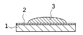
- wettability 1 (confirmation of unmelted solder alloy powder)> As a wettability evaluation 1, as shown in FIG. 3, a solder paste is used by using a mask on a Cu substrate 1 (plate thickness: about 0.70 mm) having a Ni layer 2 (layer thickness: about 2.5 ⁇ m) on the surface. 3 was printed in a shape having a diameter of 2.0 mm and a thickness of 150 ⁇ m. And the board
- a wettability tester (device name: atmosphere control type wettability tester) was started, a double cover was applied to the heater part to be heated, and nitrogen was flowed from four locations around the heater part (nitrogen flow rate: 12 L / min each). Thereafter, the heater set temperature was set to 50 ° C. higher than the melting point of each sample and heated. After the heater temperature was stabilized at the set temperature, the Cu substrate coated with the solder paste was set in the heater part and heated for 25 seconds. Thereafter, the Cu substrate was picked up from the heater part, temporarily moved to a place where the nitrogen atmosphere next to the Cu substrate was maintained, and cooled. After sufficiently cooling, it was taken out into the atmosphere.
- the bonded body was not cleaned. Each bonded body thus produced was confirmed by an optical microscope from the direction perpendicular to the surface to which the solder alloy 3 was bonded and from the surface side to which the solder alloy 3 was bonded whether there was any undissolved solder alloy powder.
- the case where the solder alloy powder remained was indicated as “X”, and the case where the solder alloy powder did not remain and the solder alloy powder melted and a solder alloy having a clean metallic luster spread on the substrate was indicated as “ ⁇ ”.
- the Si chip 4 is formed on the Ni layer 2 (layer thickness: 2.5 ⁇ m) of the Cu substrate 1 (plate thickness: 0.7 mm) as shown in FIG. A bonded body was made and the shear strength was measured. That is, the solder paste 3 is printed on the Ni layer 2 of the Cu substrate 1 in a shape of 2.0 mm ⁇ 2.0 mm and a thickness of 100 ⁇ m using a mask. A Si chip 4 having a size of 0 mm ⁇ 2.0 mm was placed, the substrates were heated and bonded as follows to form a Si chip bonded body, and the shear strength was measured.
- the joined body was manufactured using a die bonder (manufactured by Westbond, model: 3727C). First, the temperature was set to 40 ° C. higher than the melting point of the solder paste sample to be used while flowing nitrogen gas through the heater portion of the apparatus, and then the Cu substrate was placed on the heater portion, applied with the solder paste, and heated for 35 seconds to melt. The Si chip 4 was placed on the solder alloy, and scrubbing was performed for 5 seconds to form a Si chip joined body. After scrubbing, the joined body was immediately transferred to a cooling section where nitrogen gas was flowing, cooled to room temperature, and taken out into the atmosphere. The same processing was performed on each solder paste sample, and the shear strength was measured using the shear strength test for the manufactured Si chip joined body. Specifically, the bonded body was fixed to the apparatus, and the shear strength was measured by pressing the Si chip 4 from the lateral direction with a jig. The measurement results are shown in Table 2.
- the solder alloys of Samples 1 to 10 of the present invention show good characteristics in each evaluation item. That is, in the wettability evaluation 1, there was no undissolved powder. In the evaluation of wettability 2, the aspect ratio was 1.03 or less, and the wet spread spread uniformly in a circular shape. In bondability evaluation 1, the void ratio was 0.8% or less, which was a very low value. In the wettability evaluation 2, a shear strength test was conducted. As a result, the strength of the solder alloy was high and all the chips were broken at the chip, and the solder alloy was not broken. In the reliability evaluation, no defect occurred up to 500 cycles in the heat cycle test.
- the reason why such a good result was obtained was that the solder alloy of the present invention was in an appropriate composition range and the solder paste was produced under appropriate conditions.
- the metal structure of the solder alloy powder was a lamellar structure of 90% by volume or more, and each evaluation result was very good.
- the reason why such a good result was obtained is that since the proportion of the fine lamellar structure is 90% by volume or more, the solder alloy is uniformly melted and uniform bonding is possible in each part, and thus high bonding reliability. This is probably because of good results.
- the samples 15 and 16 of the comparative example, which are conventional products with a large amount of Au have good results as in the examples.
- each of the solder alloys of Samples 11 to 14 as the comparative example resulted in an undesirable result in at least any of the characteristics. That is, in Samples 11 to 14, unmelted solder alloy powder was generated, and the aspect ratio was 1.04 or more. Furthermore, the shear strength was as low as 39 to 54 MPa, the void ratio was about 10 to 22%, and voids were generated at a considerable rate. In the heat cycle test, which is an evaluation of reliability, defects occurred in all samples up to 300 cycles.
- the solder alloy of the present invention has a maximum Au content of 61%, which is much higher than the 80% by mass Au-20% by mass alloy and 88% by mass Au-12% by mass Ge alloy currently in practical use. It can be seen that the Au content is low, and therefore the cost is low.
- the oscillation frequency of the crystal resonator may shift or become unstable, so it is necessary to use a bonding material (solder material) having high bonding reliability.
- solder material solder material
- the solder material is displaced or flows out at the time of sealing, sufficient bondability cannot be obtained or a short circuit may occur. Even if voids are generated, it causes fine leaks (slight leaks) and the defect rate increases, which is not preferable.
- solder alloy after joining is superior to conventional Au-based solder alloys in terms of stress relaxation, it is excellent in jointability and reliability. Further, since the amount of Au to be used can be reduced, it is a suitable solder material for sealing a crystal resonator package which is low in cost and requires very high reliability.
Landscapes
- Chemical & Material Sciences (AREA)
- Engineering & Computer Science (AREA)
- Mechanical Engineering (AREA)
- Materials Engineering (AREA)
- Metallurgy (AREA)
- Organic Chemistry (AREA)
- Electric Connection Of Electric Components To Printed Circuits (AREA)
- Die Bonding (AREA)
Abstract
本願発明は、はんだ合金粉末とフラックスとを混合してなるはんだペーストであって、該はんだ合金粉末はその合計を100質量%としたとき、Snを27.5質量%以上33.0質量%未満含有し、Agを8.0質量%以上14.5質量%以下含有し、残部が製造上、不可避に含まれる元素を除き、Auからなることを特徴とするPbフリーAu-Sn-Ag系はんだペーストにより、電子部品の組立などで用いるのに好適な約300℃以下の固相線温度を有し、耐酸化性、濡れ性に優れると共に加工性、応力緩和特性及び信頼性にも優れ、Pbを含まず、且つAu-Sn系はんだ合金等のAu系はんだ合金に比較して格段に安価なAu-Sn-Ag系合金からなる高温用はんだペーストを提供する。
Description
本発明は高温用のPbフリーはんだペーストに関する。特に高温用として好適なAuを主成分としたAu-Sn-Ag系はんだ合金とフラックスを混合して得られるAu-Sn-Ag系はんだペースト、及び該はんだペーストを用いて接合もしくは封止した電子部品に関する。
近年、環境に有害な化学物質に対する規制がますます厳しくなってきている。この規制は電子部品などを基板に接合する目的で使用されるはんだ材料に対しても例外ではない。はんだ材料には古くから鉛が主成分として使われ続けてきたが、既にRohs指令などで規制対象物質になっている。このため、鉛(Pb)を含まないはんだ材料(以下、鉛フリーはんだ材料又は無鉛はんだ材料と称する。)の開発が盛んに行われている。
電子部品を基板に接合する際に使用するはんだ材料は、その使用限界温度によって高温用(約260℃~400℃)と中低温用(約140℃~230℃)とに大別される。高温用と中低温用のうち、中低温用はんだ材料に関してはSnを主成分とするもので鉛フリーが実用化されている。
例えば、特許文献1には「Snを主成分とし、Agを1.0~4.0重量%、Cuを2.0重量%以下、Niを1.0重量%以下、Pを0.2重量%以下含有する無鉛はんだ合金組成」が記載されている。
また、特許文献2には「Agを0.5~3.5重量%、Cuを0.5~2.0重量%含有し、残部がSnからなる合金組成の無鉛はんだ」が記載されている。
例えば、特許文献1には「Snを主成分とし、Agを1.0~4.0重量%、Cuを2.0重量%以下、Niを1.0重量%以下、Pを0.2重量%以下含有する無鉛はんだ合金組成」が記載されている。
また、特許文献2には「Agを0.5~3.5重量%、Cuを0.5~2.0重量%含有し、残部がSnからなる合金組成の無鉛はんだ」が記載されている。
一方、高温用のPbフリーはんだ材料に関しても、種々開発が行われている。例えば、特許文献3には、「Biを30~80at%含んだ溶融温度が350~500℃のBi/Agろう材」が開示されている。
また、特許文献4には、「Biを含む共晶合金に2元共晶合金を加え、更に添加元素を加えたはんだ合金」が開示されている。このはんだ合金は、4元系以上の多元系はんだ合金ではあるものの、液相線温度の調整とばらつきの減少が可能となることが示されている。
また、特許文献4には、「Biを含む共晶合金に2元共晶合金を加え、更に添加元素を加えたはんだ合金」が開示されている。このはんだ合金は、4元系以上の多元系はんだ合金ではあるものの、液相線温度の調整とばらつきの減少が可能となることが示されている。
高価な高温用のPbフリーはんだ材料としては、すでにAu-Sn合金やAu-Ge合金などが水晶デバイス、SAWフィルター、そして、MEMS等で使用されている。
Au-20質量%Sn(80質量%のAuと20質量%のSnから構成されることを意味する。以下同様。)は共晶点の組成であり、その融点は280℃である。一方、Au-12.5質量%Geは共晶点の組成であり、その融点は356℃である。
Au-Sn合金とAu-Ge合金の使い分けは、まずはこの融点の違いによる。即ち、高温用といっても比較的温度の低い箇所の接合に用いる場合はAu-Sn合金を用いる。そして、比較的高い温度の場合にはAu-Ge合金を用いる。更にAu系はんだ合金はPb系はんだ合金やSn系はんだ合金に比較し非常に硬い。特にAu-Ge合金はGeが半金属であることから、シート形状などに加工することが非常に難しい。従って、生産性や収率が悪く、コストアップの原因になっている。
Au-Sn合金もAu-Ge合金ほどではないにしても加工しづらく、プリフォーム材などへの加工時の生産性や収率は悪い。つまり、Au-20質量%Snは共晶点の組成であるとはいえ、金属間化合物から構成されている。従って、転位が移動しづらく、よって、変形しづらく、薄く圧延したり、プレスで打抜いたりするとクラックやバリが発生しやすい。
当然、Au系はんだ合金の場合、材料コストが他のはんだ材料と比較して、桁違いに高い。Au-Sn合金は、融点や加工性を活かし、特に高信頼性が要求される水晶デバイス封止用として多用されている。そして、このAu―Sn合金を安価で更に使い易くするように、例えば、次のようなAu系はんだ合金が開発されている。
特許文献5には、
「組成比(Au(wt%),Ag(wt%),Sn(wt%))が、
Au、Ag、Snの三元組成図において、
点A1(41.8, 7.6,50.5)、
点A2(62.6, 3.4,34.0)、
点A3(75.7, 3.2,21.1)、
点A4(53.6,22.1,24.3)、
点A5(30.3,33.2,36.6)
に囲まれる領域にあることを特徴とするろう材」が示されている。
本文献は「比較的低融点で扱い易く、強度、接着性に優れ、かつ安価であるろう材、及び圧電デバイスを提供する」ことを目的としている。
特許文献5には、
「組成比(Au(wt%),Ag(wt%),Sn(wt%))が、
Au、Ag、Snの三元組成図において、
点A1(41.8, 7.6,50.5)、
点A2(62.6, 3.4,34.0)、
点A3(75.7, 3.2,21.1)、
点A4(53.6,22.1,24.3)、
点A5(30.3,33.2,36.6)
に囲まれる領域にあることを特徴とするろう材」が示されている。
本文献は「比較的低融点で扱い易く、強度、接着性に優れ、かつ安価であるろう材、及び圧電デバイスを提供する」ことを目的としている。
特許文献6には、「Ag2~12質量%、Au40~55質量%、残部Snからなることを特徴とする溶融封止用高温鉛フリーはんだ合金」が示されている。
本文献は「Auの添加量が従来のAu-Sn共晶合金よりも少なくて済むばかりでなく、固相線温度が270℃以上である鉛フリーの高温はんだを提供する」こと、を目的としている。また、「容器本体と蓋部材間の接合部が耐ヒートサイクルや機械的強度に優れたパッケージを提供する」こと、を目的としている。
本文献は「Auの添加量が従来のAu-Sn共晶合金よりも少なくて済むばかりでなく、固相線温度が270℃以上である鉛フリーの高温はんだを提供する」こと、を目的としている。また、「容器本体と蓋部材間の接合部が耐ヒートサイクルや機械的強度に優れたパッケージを提供する」こと、を目的としている。
また特許文献7には、「リードフレームのピンの先端に、AgにAu20~50wt%とGe10~20wt%又はSn20~40wt%とが添加されて成るろう材が取付けられていることを特徴とするろう付きリードフレーム」が示されている。
本文献は「融点が低く、Fe-Ni合金のリードフレームを脆化せず、適度のろう流れで接合強度が安定し、しかもリードフレームの耐蝕性を低下させることのないろう材を備えたろう付きリードフレームを提供する」ことを目的としている。
本文献は「融点が低く、Fe-Ni合金のリードフレームを脆化せず、適度のろう流れで接合強度が安定し、しかもリードフレームの耐蝕性を低下させることのないろう材を備えたろう付きリードフレームを提供する」ことを目的としている。
また、特許文献8には、
「(A)AuとSnとの合計100質量部に対して、Snを55~70質量部含むAu-Sn混合粉末と、(B)フラックスとを含み、
成分(A)が、(A1)AuとSnとの合計100質量部に対して、Snを18~23.5質量部含むAu-Sn合金はんだ粉末、及び(A2)AuとSnとの合計100質量部に対して、Snを88~92質量部含むAu-Sn合金はんだ粉末を含むことを特徴とするAu-Sn合金はんだペースト」が示されている。
本文献は「280℃以下の低温で接合が可能なAu-Sn合金はんだペーストであって、かつこのペーストにより形成されたAu-Sn合金はんだは、Sn-Ag系鉛フリーはんだによるセカンドリフロー時にも溶融しない。LED素子にやさしい接合が可能で、かつ、セカンドリフロー時にも溶融することがなく、低Au化による材料コスト低減を可能とするAu-Sn合金はんだペーストを提供する」ことを目的としている。
「(A)AuとSnとの合計100質量部に対して、Snを55~70質量部含むAu-Sn混合粉末と、(B)フラックスとを含み、
成分(A)が、(A1)AuとSnとの合計100質量部に対して、Snを18~23.5質量部含むAu-Sn合金はんだ粉末、及び(A2)AuとSnとの合計100質量部に対して、Snを88~92質量部含むAu-Sn合金はんだ粉末を含むことを特徴とするAu-Sn合金はんだペースト」が示されている。
本文献は「280℃以下の低温で接合が可能なAu-Sn合金はんだペーストであって、かつこのペーストにより形成されたAu-Sn合金はんだは、Sn-Ag系鉛フリーはんだによるセカンドリフロー時にも溶融しない。LED素子にやさしい接合が可能で、かつ、セカンドリフロー時にも溶融することがなく、低Au化による材料コスト低減を可能とするAu-Sn合金はんだペーストを提供する」ことを目的としている。
高温用のPbフリーはんだ材料に関しては、上記特許文献以外にもさまざまな機関で開発されてはいるが、未だ低コストで汎用性のあるはんだ材料は見つかっていない。即ち、一般的に電子部品や基板には、熱可塑性樹脂や熱硬化性樹脂などの比較的耐熱温度の低い材料が多用されている。そのため、作業温度を400℃未満、望ましくは370℃以下にする必要がある。しかしながら、例えば特許文献3に開示されているBi/Ag合金をろう材として用いる場合は、液相線温度が400~700℃と高い。よって、接合時の作業温度も400~700℃以上になり、接合される電子部品や基板の耐熱温度を超えてしまうことになる。
実用化されているAu-Sn系はんだ材料やAu-Ge系はんだ材料は、水晶デバイス、SAWフィルター、及びMEMSなどの特に高い信頼性を必要とする箇所のはんだ付けに使用されている。しかし、Au系はんだ材料は非常に高価なAuを多量に使用するため、汎用のPb系はんだ材料やSn系はんだ材料などに比較して非常に高価であり、広く一般的に使用されているとは言い難い。加えて、Au系はんだ合金は、非常に硬く、加工しづらい。そのため、例えば、シート形状に圧延加工する際に時間がかかったり、ロールに疵がつき難い特殊な材質のものを用いたりしなければならず、コストがかかる。また、プレス成形時にもAu系はんだ合金の硬くて脆い性質のため、クラックやバリが発生し易い。従って、他のはんだ合金に比較して収率が格段に低い。ワイヤ形状に加工する場合にも似たような深刻な問題があり、非常に圧力の高い押出機を使用しても硬いため押出速度が遅く、Pb系はんだ合金の数100分の1程度の生産性しかない。
以上のような問題を含め、Au系はんだ材料は用途や使用時の形状等によってさまざまな問題がある。そのような課題を解決すべく、例えば、特許文献5に示すような技術が開示されている。即ち、特許文献5では、比較的低融点で扱いやすく、強度及び接着性に優れ、かつ安価であるろう材、及び圧電デバイスを提供する、と述べられている。更に、Au、Sn、Agそれぞれの組成範囲を限定したことで、Au含有量を従来に比して減少させつつ、封止材として同等の特性が得られるようにしている、とも述べられている。
しかし、Agを添加することによってAu-Sn合金の強度や接着性が向上する理由が記載されていない。また、封止材として同等の特性(Au-Ge合金と同等の特性と解釈できる)が得られる理由も記載されていない。即ち、Au-Ge共晶合金やAu-Sn共晶合金と同等の特性、例えば、同等の信頼性が得られる理由について記載が全くなく、発明の技術的根拠が不明である。そして以下に述べる理由により信頼性等を含め、Au-Ge共晶合金やAu-Sn共晶合金より優れるどころか、特許文献5が示す広い組成範囲の全ての領域においてAu-Ge共晶合金やAu-Sn共晶合金と同等の特性を得ることもできないと思われる。よって特許文献5の技術は実施不可能であると考える。
以下、特許文献5の技術が実施不可能であると考える理由について説明する。特許文献5は 、組成比(Au(wt%),Ag(wt%),Sn(wt%))を
Au、Ag、Snの三元組成図において、
点A1(41.8, 7.6,50.5)、
点A2(62.6, 3.4,34.0)、
点A3(75.7, 3.2,21.1)、
点A4(53.6,22.1,24.3)、
点A5(30.3,33.2,36.6)
に囲まれる領域にある組成としている。しかし、この領域はあまりにも高範囲過ぎていて、このような広い組成範囲全ての領域において目的とする特性を同じように得ることは論理的に不可能である。例えば、点A3と点A5はAu含有量が45.4質量%も異なる。このようにAu含有量に大きな差があるのに、点A3と点A5で似たような特性が得られるとは到底考えられない。Au,Sn,Agの組成比が異なれば生成される金属間化合物は異なり、液相線温度や固相線温度も大きく異なる。最も酸化しづらいAu含有量が45.4質量%も違えば当然、濡れ性も大きく変わることとなる。接合時に生成される金属間化合物の種類やその量も大きく異なり、特許文献5に示されるような広い範囲において加工性と応力緩和性について同じような優れた特性を実現できるものではない。
Au、Ag、Snの三元組成図において、
点A1(41.8, 7.6,50.5)、
点A2(62.6, 3.4,34.0)、
点A3(75.7, 3.2,21.1)、
点A4(53.6,22.1,24.3)、
点A5(30.3,33.2,36.6)
に囲まれる領域にある組成としている。しかし、この領域はあまりにも高範囲過ぎていて、このような広い組成範囲全ての領域において目的とする特性を同じように得ることは論理的に不可能である。例えば、点A3と点A5はAu含有量が45.4質量%も異なる。このようにAu含有量に大きな差があるのに、点A3と点A5で似たような特性が得られるとは到底考えられない。Au,Sn,Agの組成比が異なれば生成される金属間化合物は異なり、液相線温度や固相線温度も大きく異なる。最も酸化しづらいAu含有量が45.4質量%も違えば当然、濡れ性も大きく変わることとなる。接合時に生成される金属間化合物の種類やその量も大きく異なり、特許文献5に示されるような広い範囲において加工性と応力緩和性について同じような優れた特性を実現できるものではない。
特許文献6に記載のろう材は、Agが2~12質量%、Auが40~55質量%であることから、残部のSnは33~58質量%である。しかし、このようにSnの含有量が多いと、酸化が進行して濡れ性等が十分に得られない可能性がある。Au-20質量%Snが実用上問題なく使用されていることから、Snが30数質量%であれば、濡れ性は確保できる可能性はある。一方、Snが40質量%を越えてしまうと濡れ性の確保は困難であると推測される。また、この組成範囲では共晶合金でないため、結晶粒が粗大であったり、液相線温度と固相線温度の差が大きく接合時に溶け別れ現象が生じたりして、十分な接合信頼性を得ることは困難である。
また特許文献7に記載のろう材は、Auの含有量が最大で50質量%であり、Au原料の削減効果は非常に大きい。Snの含有量も40質量%以下(または40質量%未満)であることから、ある程度の濡れ性を確保できる可能性はある。しかし、この発明は、Fe-Ni合金製のリードフレームが脆化しないようにしたり、適度なろう流れで接合強度が安定したりするようにし、しかもリードフレームの耐蝕性を低下させないようにすることが目的である。このような観点から発明された特許文献7に示されるろう材では、例えば熱による膨張収縮による応力緩和など、半導体素子の接合用として求められる特性を満たしているとは考え難い。そして、この組成範囲では共晶合金でないため、結晶粒が粗大であったり、液相線温度と固相線温度の差が大きく、接合時に溶け別れ現象が生じたりして、十分な接合信頼性を得ることは困難であると言える。さらに、Fe-Ni合金用として発明されたろう材では半導体素子のメタライズ層やCuなどの接合用基板に適した合金を生成するとは考えにくい。このような観点から考えても、このろう材は水晶デバイス等との接合用としては適していないことは明らかである。
特許文献8には、低Auで低コストのAu-Snはんだペーストが記載されている。このようにAu系はんだ材料においては低コスト化が重要な課題であり、この市場の要求に応えることは技術進歩のために非常に重要である。しかし、特許文献8に記載の技術については、非常に大きな問題があると言える。
即ち、はんだ合金粉末は2つの組成からなるAu-Sn合金を組み合わせて使用しているが、単にこれらのはんだ合金粉末を混ぜ合わせても個々の組成の合金粉末の融点を変えることはできない。よって、(A2)(Sn=約90%)の低融点相は存在することになり高温用はんだペーストとして使用することは困難である。
特許文献8には「本発明の成分(A1)と成分(A2)を含むAu-Sn合金はんだペーストが、LED等の半導体素子と基板を接合するメカニズムは明確ではないが、260~280℃での加熱により、まず、成分(A2)が溶融して、LED等の半導体素子、基板等の被着物を濡らし、この後、溶融した成分(A2)と成分(A1)との間の拡散により、成分(A2)と成分(A1)が混合したAu-Sn合金はんだが形成されると考えられる。このメカニズムにより、LED素子にやさしい280℃以下での加熱による接合が可能であり、かつ接合後に固相線温度が250℃以上であるAu-Sn合金はんだを形成することが可能なAu-Sn合金はんだペーストを実現することができる。」と記載されている。
しかし、仮にSnリッチである(A2)成分が溶け、Au-Sn共晶点に近い成分(A1)と拡散し接合した場合、接合部のAu-Sn合金は共晶点の組成から大きく外れてしまう。そうすると、組織がラメラ組織ではなく、非常に硬くて脆い相から構成され、応力緩和性等がなく、接合信頼性も非常に低いと考えられる。また、拡散が均一に起こる保証はなく、微細なはんだ合金粉末がフラックスと混合されている中で均一に溶融、拡散する可能性は限りなくゼロに近いと言える。従って、Au含有量を下げてはんだペーストのコストを下げるという観点では非常に優れているものの、上記の理由により実用的な技術でないことは明白である。
即ち、はんだ合金粉末は2つの組成からなるAu-Sn合金を組み合わせて使用しているが、単にこれらのはんだ合金粉末を混ぜ合わせても個々の組成の合金粉末の融点を変えることはできない。よって、(A2)(Sn=約90%)の低融点相は存在することになり高温用はんだペーストとして使用することは困難である。
特許文献8には「本発明の成分(A1)と成分(A2)を含むAu-Sn合金はんだペーストが、LED等の半導体素子と基板を接合するメカニズムは明確ではないが、260~280℃での加熱により、まず、成分(A2)が溶融して、LED等の半導体素子、基板等の被着物を濡らし、この後、溶融した成分(A2)と成分(A1)との間の拡散により、成分(A2)と成分(A1)が混合したAu-Sn合金はんだが形成されると考えられる。このメカニズムにより、LED素子にやさしい280℃以下での加熱による接合が可能であり、かつ接合後に固相線温度が250℃以上であるAu-Sn合金はんだを形成することが可能なAu-Sn合金はんだペーストを実現することができる。」と記載されている。
しかし、仮にSnリッチである(A2)成分が溶け、Au-Sn共晶点に近い成分(A1)と拡散し接合した場合、接合部のAu-Sn合金は共晶点の組成から大きく外れてしまう。そうすると、組織がラメラ組織ではなく、非常に硬くて脆い相から構成され、応力緩和性等がなく、接合信頼性も非常に低いと考えられる。また、拡散が均一に起こる保証はなく、微細なはんだ合金粉末がフラックスと混合されている中で均一に溶融、拡散する可能性は限りなくゼロに近いと言える。従って、Au含有量を下げてはんだペーストのコストを下げるという観点では非常に優れているものの、上記の理由により実用的な技術でないことは明白である。
Au系はんだ材料は、はんだペーストを含めて上記のとおり、様々な改善すべき課題がある。本発明は上記課題に鑑みてなされたものであり、水晶デバイス、SAWフィルターやMEMS等の非常に高い信頼性を要求される接合においても十分に使用できる各種特性に優れた高温用Au-Sn-Ag系はんだペースト、特に、低コストで良好な濡れ性を有し、且つ、加工性、応力緩和性、及び接合信頼性等に優れたPbフリーはんだペーストを提供することを目的とする。
上記目的を達成するため、本発明によるPbフリーAu-Sn-Ag系はんだペーストは、はんだ合金粉末とフラックスとを混合してなり、該はんだ合金粉末は、その合計を100質量%としたとき、Snを27.5質量%以上33.0質量%未満含有し、Agを8.0質量%以上14.5質量%以下含有し、残部が製造上、不可避に含まれる元素を除き、Auからなることを特徴とする。
また、本発明によるPbフリーAu-Sn-Ag系はんだペーストは、前記フラックスが、ロジンを含むことを特徴とする。
また、本発明によるPbフリーAu-Sn-Ag系はんだペーストは、Snを29.0質量%以上32.0質量%以下含有し、Agを10.0質量%以上14.0質量%以下含有し、残部が製造上、不可避に含まれる元素を除き、Auからなることを特徴とする。
また、本発明によるPbフリーAu-Sn-Ag系はんだペーストは、はんだ合金粉末の金属組織の少なくとも一部が、ラメラ組織であることを特徴とする。
また、本発明によるPbフリーAu-Sn-Ag系はんだペーストは、はんだ合金粉末の金属組織がラメラ組織であり、その割合が90体積%以上であることを特徴とする。
また、本発明は、上記PbフリーAu-Sn-Ag系はんだペーストを用いて接合されていることを特徴とするSi半導体素子接合体を提供する。
また、本発明は、上記PbフリーAu-Sn-Ag系はんだペーストを用いて封止されていることを特徴とする水晶振動子封止素子を提供する。
本発明によれば、水晶デバイス、SAWフィルター、そして、MEMSなどの非常に高い信頼性を要求される箇所に使われるはんだ材料を従来のAu系はんだ材料よりも安価に提供できる。
さらに、本発明のはんだ合金粉末は共晶金属を基本としており、よって金属組織が細かいラメラ組織になっていて優れた柔軟性を有し応力緩和性、接合信頼性に優れ、かつ、フラックスと混合してはんだペーストとすることによって優れた濡れ性、接合性を有するAu系はんだペーストを提供することができる。従って、工業的な貢献度は極めて高い。
本発明者は、鋭意研究を重ねた結果、AuとSnとAgの三元共晶点の組成付近を基本としているAu-Sn-Ag系はんだ合金粉末とフラックスを混合してなるはんだペーストにおいて、所定のはんだ合金組成範囲を満たすと次の特性や効果を有することを見出し、本発明に至った。まず、Au-Sn合金に比べて柔らかく、加工性や応力緩和性に優れ、且つ、高価なAuの一部をSnとAgで代替することによってAu含有量を大幅に下げて、はんだ合金のコストを下げたAu系合金粉末を得ることができる。更に、フラックスと混ぜてはんだペーストとすることにより形状自由度が大きくなり、濡れ広がり性、接合信頼性等に優れた接合材となる。
以下、本発明のAu-Sn-Ag系はんだペーストにおけるはんだ合金粉末、フラックスについて詳しく説明する。まず本発明のAu-Sn-Ag系はんだ合金の組成は、Snを27.5質量%以上33.0質量%未満含有し、Agを8.0質量%以上14.5質量%以下含有し、残部が製造上不可避に含まれる元素を除きAuから構成されることを特徴とする。
本発明のはんだ合金は、非常に高コストであるAu系はんだ合金のコストを下げるとともに、優れた加工性や応力緩和性を持たせるために柔らかい金属であるAgを含有させ、かつ三元共晶付近の組成とすることにより結晶を微細化して成るものである(図1参照)。つまり、Au-Sn-Ag三元共晶点の組成であるAu=57.2質量%、Sn=30.8質量%、Ag=12.0質量%(at%表示では、Au=43.9at%、Sn=39.3at%、Ag=16.8at%)を基本的な組成とする。これにより、結晶構造がラメラ組織となり、加工性、応力緩和性等が格段に向上し、かつ、Sn、Agを多く含有させることができ、よってAu含有量が低減でき、大きなコスト削減効果を得ることができる。また、反応性が高く、酸化し難いAgを多く含有することによって良好な濡れ性、接合性を得ることができる。以下、本発明に使用するはんだ合金に必須の元素について、さらに詳しく説明する。
<Au>
Auは本発明に使用するはんだ合金の主成分であり、当然、必須の元素である。Auは非常に酸化しづらいため、高い信頼性が要求される電子部品類の接合や封止用のはんだ材料の成分として、特性面においては最も適している。このため、水晶デバイスやSAWフィルターの封止用としてAu系はんだ材料が多用されている。本発明に使用するはんだ合金もAuを基本とし、このような高信頼性を要求される技術分野に属するはんだ材料を提供する。ただし、Auは非常に高価な金属であるため、コスト面からするとできるだけ使わない方がよい。このため、一般的なレベルの信頼性を要求される電子部品にはほとんど使用されていない。本発明に使用するはんだ合金は、濡れ性や接合性といった特性面ではAu-20質量%Snはんだ合金や、Au-12.5質量%Geはんだ合金と同等以上である。且つ、柔軟性、加工性を向上させ、加えてAu含有量を減らしてコストを下げるべく、Au-Sn-Ag系の三元共晶点の組成付近の合金としている。
Auは本発明に使用するはんだ合金の主成分であり、当然、必須の元素である。Auは非常に酸化しづらいため、高い信頼性が要求される電子部品類の接合や封止用のはんだ材料の成分として、特性面においては最も適している。このため、水晶デバイスやSAWフィルターの封止用としてAu系はんだ材料が多用されている。本発明に使用するはんだ合金もAuを基本とし、このような高信頼性を要求される技術分野に属するはんだ材料を提供する。ただし、Auは非常に高価な金属であるため、コスト面からするとできるだけ使わない方がよい。このため、一般的なレベルの信頼性を要求される電子部品にはほとんど使用されていない。本発明に使用するはんだ合金は、濡れ性や接合性といった特性面ではAu-20質量%Snはんだ合金や、Au-12.5質量%Geはんだ合金と同等以上である。且つ、柔軟性、加工性を向上させ、加えてAu含有量を減らしてコストを下げるべく、Au-Sn-Ag系の三元共晶点の組成付近の合金としている。
<Sn>
Snは本発明に使用するはんだ合金において必須の元素であり、基本を成す元素である。Au-Snはんだ合金は、通常、共晶点付近の組成、つまりAu-20質量%Sn付近の組成で使用される。これによって、固相線温度が280℃になり、かつ、結晶が微細化し、比較的柔軟性が得られるのである。しかし、共晶合金と言ってもAu-20質量%Sn合金は、Au1Sn1金属間化合物とAu5Sn1金属間化合物から構成されているため、硬くて脆い。このため、加工しづらく、例えば、圧延によってシート状に加工する際には少しずつしか薄くしていくことができない。このため、生産性が悪かったり、圧延時に多数のクラックが入って収率が悪かったりするが、金属間化合物の硬くて脆い性質は一般的には変えることができない。このように硬くて脆い材料ではあるが、酸化しにくく濡れ性、信頼性に優れるため、高信頼性を要求される用途に使用されているのである。
本発明に使用するはんだ合金は、Au1Sn1金属間化合物とζ相(ζ相はAu-Sn-Ag金属間化合物であり、その組成の比率はat%でAu:Sn:Ag=30.1:16.1:53.8である。参考文献:Ternary Alloys, A Comprehensive Compendium of Evaluated Constitutional Data and Phase Diagrams, Edited by G. Petzow and Effenberg, VCH)から構成され、かつ共晶点付近の組成を基本とする。このζ相が比較的柔軟性を有すること、そして共晶点付近を基本組成としておりラメラ組織を形成することから、本発明に使用するはんだ合金は加工性、応力緩和性等に優れることになるのである。そして融点も下げることができAu-Ge合金の共晶点温度と大差ない370℃の共晶点温度を有するのである。このような高温用はんだ合金として適切な融点を持つことも本発明に使用するはんだ合金の優れる点の一つである。
Snの含有量は27.5質量%以上33.0質量%未満である。27.5質量%未満であると結晶粒が大きくなってしまい柔軟性、加工性向上等の効果が十分に発揮されない。その上、液相線温度と固相線温度の差が大きくなり過ぎて溶け別れ現象などが生じてしまう。更にAu含有量も多くなりやすくなるため、コスト削減効果も限定されたものとなってしまう。一方、Snの含有量が33.0質量%以上になると共晶点の組成から外れ過ぎてしまい、結晶粒の粗大化、液相線温度と固相線温度の差が大きくなってしまう問題が生じる。加えて、Sn含有量が多くなり過ぎると、Au-Sn-Ag合金が酸化しやすくなってしまい、Au系はんだ材料の特徴である良好な濡れ性を失い、よって、高い接合信頼性を得ることが難しくなってしまう。
Sn含有量が29.0質量%以上32.0質量%以下であれば、一層、共晶点の組成に近く、結晶粒微細化効果が得られ、かつ溶け別れ現象などが生じづらく好ましい。
Snは本発明に使用するはんだ合金において必須の元素であり、基本を成す元素である。Au-Snはんだ合金は、通常、共晶点付近の組成、つまりAu-20質量%Sn付近の組成で使用される。これによって、固相線温度が280℃になり、かつ、結晶が微細化し、比較的柔軟性が得られるのである。しかし、共晶合金と言ってもAu-20質量%Sn合金は、Au1Sn1金属間化合物とAu5Sn1金属間化合物から構成されているため、硬くて脆い。このため、加工しづらく、例えば、圧延によってシート状に加工する際には少しずつしか薄くしていくことができない。このため、生産性が悪かったり、圧延時に多数のクラックが入って収率が悪かったりするが、金属間化合物の硬くて脆い性質は一般的には変えることができない。このように硬くて脆い材料ではあるが、酸化しにくく濡れ性、信頼性に優れるため、高信頼性を要求される用途に使用されているのである。
本発明に使用するはんだ合金は、Au1Sn1金属間化合物とζ相(ζ相はAu-Sn-Ag金属間化合物であり、その組成の比率はat%でAu:Sn:Ag=30.1:16.1:53.8である。参考文献:Ternary Alloys, A Comprehensive Compendium of Evaluated Constitutional Data and Phase Diagrams, Edited by G. Petzow and Effenberg, VCH)から構成され、かつ共晶点付近の組成を基本とする。このζ相が比較的柔軟性を有すること、そして共晶点付近を基本組成としておりラメラ組織を形成することから、本発明に使用するはんだ合金は加工性、応力緩和性等に優れることになるのである。そして融点も下げることができAu-Ge合金の共晶点温度と大差ない370℃の共晶点温度を有するのである。このような高温用はんだ合金として適切な融点を持つことも本発明に使用するはんだ合金の優れる点の一つである。
Snの含有量は27.5質量%以上33.0質量%未満である。27.5質量%未満であると結晶粒が大きくなってしまい柔軟性、加工性向上等の効果が十分に発揮されない。その上、液相線温度と固相線温度の差が大きくなり過ぎて溶け別れ現象などが生じてしまう。更にAu含有量も多くなりやすくなるため、コスト削減効果も限定されたものとなってしまう。一方、Snの含有量が33.0質量%以上になると共晶点の組成から外れ過ぎてしまい、結晶粒の粗大化、液相線温度と固相線温度の差が大きくなってしまう問題が生じる。加えて、Sn含有量が多くなり過ぎると、Au-Sn-Ag合金が酸化しやすくなってしまい、Au系はんだ材料の特徴である良好な濡れ性を失い、よって、高い接合信頼性を得ることが難しくなってしまう。
Sn含有量が29.0質量%以上32.0質量%以下であれば、一層、共晶点の組成に近く、結晶粒微細化効果が得られ、かつ溶け別れ現象などが生じづらく好ましい。
<Ag>
Agは本発明に使用するはんだ合金において必須の元素であり、三元共晶の合金とするために欠かすことのできない元素である。Au-Sn-Agの三元共晶点付近の組成とすることにより、はじめて優れた柔軟性や加工性、応力緩和性、適した融点等を得ることができる。更に大幅にAu含有量を下げることが可能となり、よって大きなコスト削減を実現できる。Ag添加は濡れ性向上の効果も有する。即ち、Agを添加することによりAu-Sn-Ag合金と基板等の最上面に使用されるCu、Niなどとの反応性が向上し、濡れ性を向上させることができる。当然、半導体素子の接合面によく使用されるAgやAuメタライズ層との反応性に優れることは言うまでもない。
このように優れた効果を発揮するAgの含有量は8.0質量%以上14.5質量%以下である。Agの含有量が8.0質量%未満では共晶点の組成から外れ過ぎてしまい、液相線温度が高くなり過ぎたり、結晶粒が粗大化したりしてしまい、良好な接合を得ることが難しくなる。一方、Agの含有量が14.5質量%を越えてしまった場合も、液相線温度が高くなり、溶け分かれ現象を生じたり、結晶粒の粗大化が問題になったりしてしまう。
Agの含有量が10.0質量%以上14.0質量%以下であれば共晶点の組成に近く、Agを含有させた効果がより一層現れて好ましい。
Agは本発明に使用するはんだ合金において必須の元素であり、三元共晶の合金とするために欠かすことのできない元素である。Au-Sn-Agの三元共晶点付近の組成とすることにより、はじめて優れた柔軟性や加工性、応力緩和性、適した融点等を得ることができる。更に大幅にAu含有量を下げることが可能となり、よって大きなコスト削減を実現できる。Ag添加は濡れ性向上の効果も有する。即ち、Agを添加することによりAu-Sn-Ag合金と基板等の最上面に使用されるCu、Niなどとの反応性が向上し、濡れ性を向上させることができる。当然、半導体素子の接合面によく使用されるAgやAuメタライズ層との反応性に優れることは言うまでもない。
このように優れた効果を発揮するAgの含有量は8.0質量%以上14.5質量%以下である。Agの含有量が8.0質量%未満では共晶点の組成から外れ過ぎてしまい、液相線温度が高くなり過ぎたり、結晶粒が粗大化したりしてしまい、良好な接合を得ることが難しくなる。一方、Agの含有量が14.5質量%を越えてしまった場合も、液相線温度が高くなり、溶け分かれ現象を生じたり、結晶粒の粗大化が問題になったりしてしまう。
Agの含有量が10.0質量%以上14.0質量%以下であれば共晶点の組成に近く、Agを含有させた効果がより一層現れて好ましい。
<金属組成>
本発明において、Au-Sn-Ag系はんだ合金の金属組織の少なくとも一部がラメラ組織であり、その割合が90体積%以上であることが好ましい。ラメラ組織は縞状の組織の縞の間隔が0.1μm以上2.0μm以下である金属組織を言う。例えば、図2における四角で囲んだ部分は、本発明が定義するラメラ組織である。このように接合後のはんだ合金組織が細かいラメラ組織になることによって、一層、クラックが発生しづらく且つ進展しづらくなり、よってより高い接合信頼性を得ることができる。
本発明において、Au-Sn-Ag系はんだ合金の金属組織の少なくとも一部がラメラ組織であり、その割合が90体積%以上であることが好ましい。ラメラ組織は縞状の組織の縞の間隔が0.1μm以上2.0μm以下である金属組織を言う。例えば、図2における四角で囲んだ部分は、本発明が定義するラメラ組織である。このように接合後のはんだ合金組織が細かいラメラ組織になることによって、一層、クラックが発生しづらく且つ進展しづらくなり、よってより高い接合信頼性を得ることができる。
<フラックス>
本発明のはんだペーストに使用するフラックスの種類は特に限定がなく、例えば、樹脂系、無機塩化物系、有機ハロゲン化物系などを用いてよい。ここでは、最も一般的なフラックスである、ベース材にロジンを使用してこれに活性剤および溶剤を添加したものについて述べる。
本発明のはんだペーストに使用するフラックスの種類は特に限定がなく、例えば、樹脂系、無機塩化物系、有機ハロゲン化物系などを用いてよい。ここでは、最も一般的なフラックスである、ベース材にロジンを使用してこれに活性剤および溶剤を添加したものについて述べる。
例として示すこのフラックスは、フラックス全量を100質量%とした場合、ベース材であるロジンが20~30質量%、活性剤が0.2~1質量%、溶剤が70~80質量%程度となるように配合することが好ましい。これにより良好な濡れ性および接合性を有するはんだペーストを得ることができる。またチキソ剤を含有させチキソ性を調整するとより一層使い易いはんだペーストとなり得る。ベース材としてのロジンには、例えばウッドレジンロジン、ガムロジン、トール油ロジンなどの天然の未変性なロジンを使用してもよいし、ロジンエステル、水素添加ロジン、ロジン変性樹脂、重合ロジンなどの変性ロジンを使用してもよい。
溶剤には、アセトン、アミルベンゼン、n-アミンアルコール、ベンゼン、四塩化炭素、メチルアルコール、エチルアルコール、イソプロピルアルコール、n-ブタノール、イソブチルアルコール、メチルエチルケトン、トルエン、テレピン油、キシレン、シクロヘキサン、エチレングリコールモノフェニルエーテル、エチレングリコールモノブチルエーテル、四塩化炭素、トリクロロエタン、アルカンジオール、アルキレングリコール、ブタジオール、トリエチレングリコール、テトラエチレングリコール、テトラデカンなどを使用することができる。
活性剤には、リン酸、塩化ナトリウム、塩化アンモニウム、塩化亜鉛、塩化第一錫、アニリン塩酸塩、ヒドラジン塩酸塩、臭化セチルピリジン、フェニルヒドラジン塩酸塩、テトラクロルナフタレン、メチルヒドラジン塩酸塩、メチルアミン塩酸塩、エチルアミン塩酸塩、ジエチルアミン塩酸塩、ブチルアミン塩酸塩、安息香酸、ステアリン酸、乳酸、クエン酸、シュウ酸、コハク酸、アジピン酸、ヒバシン酸、トリエタノールアミン、ジフェニルグアニジン、ジフェニルグアニジンHBr、エリトリトール、キシリトリトール、ソルボトール、リビトールなどを使用することができる。
またチキソ剤を含有させてチキソ性を調整するとより一層使い易いはんだペーストになり得る。チキソ剤としては例えば、ステアリン酸アミド、オレイン酸アミド、エルカ酸アミドを用いることができる。
またチキソ剤を含有させてチキソ性を調整するとより一層使い易いはんだペーストになり得る。チキソ剤としては例えば、ステアリン酸アミド、オレイン酸アミド、エルカ酸アミドを用いることができる。
これらの溶剤および活性剤の中から目的に合った物質を選択し、それらの添加量を適宜調整することによって好適なフラックスが得られる。例えば、はんだ合金や基板等の接合面の酸化膜が強固である場合は、ロジンや活性剤を多めに添加し、溶剤で粘性や流動性を調整するのが好ましい。
上記はんだ合金とフラックスとを混合することによって得られるはんだペーストは、フラックスの作用によって非常に優れた濡れ性を備えている。その上、はんだ合金については加工に困難を伴うシート形状等に加工する必要がなく、加工しやすい粉末状で使用することができる。
そして、本発明の高温用Pbフリーはんだペーストを、電子部品と基板との接合に使用することによって、ヒートサイクルが繰り返される環境などの過酷な条件下で使用される場合であっても、耐久性のある信頼性の高い電子部品用基板を提供することができる。よって、この電子部品用基板を、例えば、サイリスタやインバータなどのパワー半導体装置、自動車などに搭載される各種制御装置、太陽電池などの過酷な条件下で使用される装置に搭載することによって、それら各種装置の信頼性をより一層高めることができる。また、このように優れた本発明によるはんだペーストは、水晶振動子の封止用としても非常に適するものであり、例えば図6のような水晶振動子パッケージの封止用として使用できる。
以下、実施例に基き本発明を更に詳細に説明するが、本発明はこれら実施例によって何ら限定されるものではない。
まず、原料としてそれぞれ純度99.99質量%以上のAu、SnおよびAgと、比較用のAu-Ge合金のためのGeを準備した。大きな薄片やバルク状の原料については、溶解後の合金においてサンプリング場所による組成のバラツキがなく均一になるようにするため切断、粉砕等を行い、3mm角以下の大きさに細かくした。次に、高周波溶解炉用グラファイトるつぼに、これら原料から所定量を秤量して入れた。
原料の入ったるつぼを高周波溶解炉に入れ、酸化を抑制するために窒素を原料1kg当たり0.7L/分以上の流量で流した。この状態で溶解炉の電源を入れ、原料を加熱溶融させた。金属が溶融しはじめたら混合棒でよく攪拌し、局所的な組成のばらつきが起きないように均一に混ぜた。十分溶融したことを確認した後、高周波電源を切り、速やかにるつぼを取り出し、るつぼ内の溶湯をはんだ母合金の鋳型に流し込んだ。鋳型には、粉末を製造するための気相中アトマイズ用に内径140mmの円柱形状のものを使用した。
このようにして、原料の混合比率を変えた以外は上記と同様にして、試料1~16のはんだ母合金を作製した。これらの試料1~16の各はんだ母合金について、ICP発光分光分析器(SHIMAZU S-8100)を用いて組成分析を行った。得られた分析結果を下記表1に示した。
まず、原料としてそれぞれ純度99.99質量%以上のAu、SnおよびAgと、比較用のAu-Ge合金のためのGeを準備した。大きな薄片やバルク状の原料については、溶解後の合金においてサンプリング場所による組成のバラツキがなく均一になるようにするため切断、粉砕等を行い、3mm角以下の大きさに細かくした。次に、高周波溶解炉用グラファイトるつぼに、これら原料から所定量を秤量して入れた。
原料の入ったるつぼを高周波溶解炉に入れ、酸化を抑制するために窒素を原料1kg当たり0.7L/分以上の流量で流した。この状態で溶解炉の電源を入れ、原料を加熱溶融させた。金属が溶融しはじめたら混合棒でよく攪拌し、局所的な組成のばらつきが起きないように均一に混ぜた。十分溶融したことを確認した後、高周波電源を切り、速やかにるつぼを取り出し、るつぼ内の溶湯をはんだ母合金の鋳型に流し込んだ。鋳型には、粉末を製造するための気相中アトマイズ用に内径140mmの円柱形状のものを使用した。
このようにして、原料の混合比率を変えた以外は上記と同様にして、試料1~16のはんだ母合金を作製した。これらの試料1~16の各はんだ母合金について、ICP発光分光分析器(SHIMAZU S-8100)を用いて組成分析を行った。得られた分析結果を下記表1に示した。

<はんだ合金粉末の製造方法>
はんだペースト用合金粉末の製造方法は特に限定されないが、アトマイズ法により製造するのが一般的である。アトマイズ法は気相中、液相中どちらで行ってもよく、目的とするはんだ合金粉末の粒径や粒度分布等を考慮して選定すればよい。本実施例では、生産性が高く、比較的細かい粉末の製造ができる気相中アトマイズ法によりはんだ合金粉末を作製した。
具体的には、気相中アトマイズ装置(日新技研株式会社製)を用いて、高周波溶解方式によって気相中アトマイズを行った。まず、上記試料1~16のはんだ母合金をそれぞれ1ロットずつ粉末に加工していった。具体的には母合金の試料を高周波溶解るつぼに投入し、蓋をして密閉した後、窒素フローし、実質的に酸素が無い状態にした。試料排出口や回収容器部分も同様に窒素フローして酸素が無い状態にした。
この状態で高周波電源のスイッチを入れ、はんだ母合金を450℃以上に加熱し、合金が十分溶融した状態で溶融したはんだ母合金に窒素で圧力を加え、アトマイズした。このようにして作製されたはんだ合金粉末を容器に回収し、この容器中で十分に冷却してから大気中に取り出した。十分に冷却してから取り出す理由は、高温状態で取り出すと発火したり、はんだ合金粉末が酸化して濡れ性等の効果を下げてしまうからである。
このようにして製造した各粉末をそれぞれ目開きが20μmと50μmの篩で分級して、直径が20~50μmの合金粉末試料を得た。
はんだペースト用合金粉末の製造方法は特に限定されないが、アトマイズ法により製造するのが一般的である。アトマイズ法は気相中、液相中どちらで行ってもよく、目的とするはんだ合金粉末の粒径や粒度分布等を考慮して選定すればよい。本実施例では、生産性が高く、比較的細かい粉末の製造ができる気相中アトマイズ法によりはんだ合金粉末を作製した。
具体的には、気相中アトマイズ装置(日新技研株式会社製)を用いて、高周波溶解方式によって気相中アトマイズを行った。まず、上記試料1~16のはんだ母合金をそれぞれ1ロットずつ粉末に加工していった。具体的には母合金の試料を高周波溶解るつぼに投入し、蓋をして密閉した後、窒素フローし、実質的に酸素が無い状態にした。試料排出口や回収容器部分も同様に窒素フローして酸素が無い状態にした。
この状態で高周波電源のスイッチを入れ、はんだ母合金を450℃以上に加熱し、合金が十分溶融した状態で溶融したはんだ母合金に窒素で圧力を加え、アトマイズした。このようにして作製されたはんだ合金粉末を容器に回収し、この容器中で十分に冷却してから大気中に取り出した。十分に冷却してから取り出す理由は、高温状態で取り出すと発火したり、はんだ合金粉末が酸化して濡れ性等の効果を下げてしまうからである。
このようにして製造した各粉末をそれぞれ目開きが20μmと50μmの篩で分級して、直径が20~50μmの合金粉末試料を得た。
<はんだ合金粉末のラメラ組織の割合の算出>
本発明の実施例である試料1~10の合金粉末について、はんだ合金粉末のラメラ組織の割合を測定した。ラメラ組織の割合の測定は、はんだ合金粉末を樹脂に埋め込み、研磨してはんだ合金粉末の断面を出し、任意の10カ所で10μm×10μmの範囲におけるラメラ組織の断面積の割合を測定し、その10点の平均値を3/2乗することによって算出した値を体積%として用いた。その結果は表1に示したとおりである。
本発明の実施例である試料1~10の合金粉末について、はんだ合金粉末のラメラ組織の割合を測定した。ラメラ組織の割合の測定は、はんだ合金粉末を樹脂に埋め込み、研磨してはんだ合金粉末の断面を出し、任意の10カ所で10μm×10μmの範囲におけるラメラ組織の断面積の割合を測定し、その10点の平均値を3/2乗することによって算出した値を体積%として用いた。その結果は表1に示したとおりである。
<はんだペーストの製造方法>
次に、はんだ母合金の試料からそれぞれ作製したはんだ合金粉末をそれぞれフラックスと混合し、はんだペーストを作製した。本発明においてフラックスはとくに限定されないが、本実施例においてはフラックスには、ベース材として重合ロジンを、活性剤としてジエチルアミン塩酸塩((C2H5)2NH・HCl)を、溶剤としてエチルアルコールを用いた。それぞれの含有量はフラックスを100質量%として、重合ロジンが23質量%、ジエチルアミン塩酸塩が0.3質量%、残部をエチルアルコールとした。このフラックスと上記はんだ合金粉末とをフラックス9.2質量%、はんだ合金粉末90.8質量%の割合で調合し、小型ブレンダーを用いて混合してはんだペーストとした。
このようにして、上記表1に示す試料1~16のはんだ母合金からそれぞれ試料1~16のはんだペーストを作製した。そして、これら試料1~16のはんだペーストの各々に対して、下記に示す評価を行った。即ち、濡れ性の評価1としてはんだ合金粉末の溶け残りの確認を行い、濡れ性の評価2として縦横比の測定を行い、接合性の評価1としてボイド率の測定を行い、接合性の評価2としてシェア強度の測定を行い、信頼性の評価としてヒートサイクル試験を行った。
次に、はんだ母合金の試料からそれぞれ作製したはんだ合金粉末をそれぞれフラックスと混合し、はんだペーストを作製した。本発明においてフラックスはとくに限定されないが、本実施例においてはフラックスには、ベース材として重合ロジンを、活性剤としてジエチルアミン塩酸塩((C2H5)2NH・HCl)を、溶剤としてエチルアルコールを用いた。それぞれの含有量はフラックスを100質量%として、重合ロジンが23質量%、ジエチルアミン塩酸塩が0.3質量%、残部をエチルアルコールとした。このフラックスと上記はんだ合金粉末とをフラックス9.2質量%、はんだ合金粉末90.8質量%の割合で調合し、小型ブレンダーを用いて混合してはんだペーストとした。
このようにして、上記表1に示す試料1~16のはんだ母合金からそれぞれ試料1~16のはんだペーストを作製した。そして、これら試料1~16のはんだペーストの各々に対して、下記に示す評価を行った。即ち、濡れ性の評価1としてはんだ合金粉末の溶け残りの確認を行い、濡れ性の評価2として縦横比の測定を行い、接合性の評価1としてボイド率の測定を行い、接合性の評価2としてシェア強度の測定を行い、信頼性の評価としてヒートサイクル試験を行った。
<濡れ性の評価1(はんだ合金粉末の溶け残りの確認)>
濡れ性の評価1として、図3に示すように表面にNi層2(層厚:約2.5μm)を有するCu基板1(板厚:約0.70mm)上にマスクを使って、はんだペースト3を直径2.0mm、厚さ150μmの形状に印刷した。そして、そのはんだペースト3が印刷された基板を以下のように加熱、接合して接合体を作り、光学顕微鏡ではんだ合金粉末の溶け残りが無いか確認した。
まず、濡れ性試験機(装置名:雰囲気制御式濡れ性試験機)を起動し、加熱されるヒーター部分に二重のカバーをしてヒーター部の周囲4箇所から窒素を流した(窒素流量:各12L/分)。その後、ヒーター設定温度を各試料の融点より50℃高く設定して加熱した。ヒーター温度が設定温度で安定した後、はんだペーストを塗布したCu基板をヒーター部にセッティングし、25秒加熱した。その後、Cu基板をヒーター部から取り上げて、その横の窒素雰囲気が保たれている場所に一旦移して冷却した。十分に冷却した後、大気中に取り出した。はんだ合金粉末の溶け残りを確認するため接合体の洗浄等はあえて行わなかった。
このようにして作った各接合体をはんだ合金3が接合された面と直角の方向から、そしてはんだ合金3が接合された面側から光学顕微鏡ではんだ合金粉末の溶け残りが無いか確認した。はんだ合金粉末が残っていた場合を「×」、はんだ合金粉末が残っておらずはんだ合金粉末が溶けてきれいな金属光沢のあるはんだ合金が基板に濡れ広がっていた場合を「○」とした。
濡れ性の評価1として、図3に示すように表面にNi層2(層厚:約2.5μm)を有するCu基板1(板厚:約0.70mm)上にマスクを使って、はんだペースト3を直径2.0mm、厚さ150μmの形状に印刷した。そして、そのはんだペースト3が印刷された基板を以下のように加熱、接合して接合体を作り、光学顕微鏡ではんだ合金粉末の溶け残りが無いか確認した。
まず、濡れ性試験機(装置名:雰囲気制御式濡れ性試験機)を起動し、加熱されるヒーター部分に二重のカバーをしてヒーター部の周囲4箇所から窒素を流した(窒素流量:各12L/分)。その後、ヒーター設定温度を各試料の融点より50℃高く設定して加熱した。ヒーター温度が設定温度で安定した後、はんだペーストを塗布したCu基板をヒーター部にセッティングし、25秒加熱した。その後、Cu基板をヒーター部から取り上げて、その横の窒素雰囲気が保たれている場所に一旦移して冷却した。十分に冷却した後、大気中に取り出した。はんだ合金粉末の溶け残りを確認するため接合体の洗浄等はあえて行わなかった。
このようにして作った各接合体をはんだ合金3が接合された面と直角の方向から、そしてはんだ合金3が接合された面側から光学顕微鏡ではんだ合金粉末の溶け残りが無いか確認した。はんだ合金粉末が残っていた場合を「×」、はんだ合金粉末が残っておらずはんだ合金粉末が溶けてきれいな金属光沢のあるはんだ合金が基板に濡れ広がっていた場合を「○」とした。
<濡れ性の評価2(縦横比の測定)>
濡れ性の評価2として、はんだ合金粉末の溶け残りの確認の際に作った接合体と同様の接合体を作り、その接合体をアルコールで洗浄、その後真空乾燥して、その基板に濡れ広がったはんだ合金の縦横比を測定した。得られた接合体、即ち図3に示すようにCu基板1のNi層2上にはんだ合金3が接合された接合体について、濡れ広がったはんだ合金3の縦横比を求めた。
具体的には、図4に示す最大のはんだ濡れ広がり長さである長径X1、最小のはんだ濡れ広がり長さである短径X2を測定し、下記計算式1により縦横比を算出した。計算式1の縦横比が1に近いほど基板上に円形状に濡れ広がっており、濡れ広がり性がよいと判断できる。1より大きくなるに従い、濡れ広がり形状が円形からずれていき、溶融はんだ合金の移動距離にバラつきが出て反応が不均一になり、合金層の厚みや成分のばらつきが大きくなったりして、均一で良好な接合ができなくなってしまう。ある方向に多くのはんだ合金が流れるように広がった場合は、はんだ合金量が過剰な箇所とはんだ合金が無い箇所ができてしまうことがあり、接合不良や場合よっては接合できなかったりしてしまう。接合体の縦横比の測定結果を表2に示す。
[計算式1]
縦横比=長径÷短径
濡れ性の評価2として、はんだ合金粉末の溶け残りの確認の際に作った接合体と同様の接合体を作り、その接合体をアルコールで洗浄、その後真空乾燥して、その基板に濡れ広がったはんだ合金の縦横比を測定した。得られた接合体、即ち図3に示すようにCu基板1のNi層2上にはんだ合金3が接合された接合体について、濡れ広がったはんだ合金3の縦横比を求めた。
具体的には、図4に示す最大のはんだ濡れ広がり長さである長径X1、最小のはんだ濡れ広がり長さである短径X2を測定し、下記計算式1により縦横比を算出した。計算式1の縦横比が1に近いほど基板上に円形状に濡れ広がっており、濡れ広がり性がよいと判断できる。1より大きくなるに従い、濡れ広がり形状が円形からずれていき、溶融はんだ合金の移動距離にバラつきが出て反応が不均一になり、合金層の厚みや成分のばらつきが大きくなったりして、均一で良好な接合ができなくなってしまう。ある方向に多くのはんだ合金が流れるように広がった場合は、はんだ合金量が過剰な箇所とはんだ合金が無い箇所ができてしまうことがあり、接合不良や場合よっては接合できなかったりしてしまう。接合体の縦横比の測定結果を表2に示す。
[計算式1]
縦横比=長径÷短径
<接合性の評価1(ボイド率の測定)>
接合性の評価1として、はんだ合金粉末の溶け残りの確認の際に作った接合体と同様の接合体を作り、その接合体をアルコールで洗浄し、その後真空乾燥して、はんだ合金の濡れ広がった接合体に関して以下のようにボイド率を測定した。
図3に示す接合体について、Ni2層を介してはんだ合金3が接合されたCu基板1のボイド率をX線透過装置(株式会社東芝製、TOSMICRON-6125)を用いて測定した。具体的には、はんだ合金3とCu基板1との接合面をはんだ合金3の接合された面側から垂直にX線を透過し、得られたX線像から求めた各面積より下記計算式2を用いてボイド率を算出した。接合体のボイド率の測定結果を表2に示す。
[計算式2]
ボイド率(%)=ボイド面積÷(ボイド面積+はんだ合金とCu基板の接合面積)×100
接合性の評価1として、はんだ合金粉末の溶け残りの確認の際に作った接合体と同様の接合体を作り、その接合体をアルコールで洗浄し、その後真空乾燥して、はんだ合金の濡れ広がった接合体に関して以下のようにボイド率を測定した。
図3に示す接合体について、Ni2層を介してはんだ合金3が接合されたCu基板1のボイド率をX線透過装置(株式会社東芝製、TOSMICRON-6125)を用いて測定した。具体的には、はんだ合金3とCu基板1との接合面をはんだ合金3の接合された面側から垂直にX線を透過し、得られたX線像から求めた各面積より下記計算式2を用いてボイド率を算出した。接合体のボイド率の測定結果を表2に示す。
[計算式2]
ボイド率(%)=ボイド面積÷(ボイド面積+はんだ合金とCu基板の接合面積)×100
<接合性の評価2(シェア強度の測定)>
はんだ合金の接合性を確認するため、はんだペースト試料を用いて図5に示すようなCu基板1(板厚:0.7mm)のNi層2(層厚:2.5μm)上にSiチップ4が接合された接合体を作り、シェア強度を測定した。即ち、Cu基板1のNi層2上にマスクを使ってはんだペースト3を2.0mm×2.0mm、厚さ100μmの形状に印刷し、基板を加熱後、そのはんだペースト3の上に2.0mm×2.0mmのSiチップ4を置き、その基板を以下のように加熱、接合してSiチップ接合体を作り、そのシェア強度を測定した。
接合体の作製はダイボンダー(Westbond製、型式:3727C)を用いて行った。まず装置のヒーター部に窒素ガスを流しながら使用するはんだペースト試料の融点より40℃高い温度になるようにした後、ヒーター部にCu基板を乗せはんだペーストを塗布した後35秒加熱し、溶融したはんだ合金の上にSiチップ4を載せスクラブを5秒かけSiチップ接合体を形成した。スクラブ終了後、接合体を速やかに窒素ガスの流れている冷却部に移し、室温まで冷却後、大気中に取り出した。同様の処理を各はんだペースト試料で行い、作製したSiチップ接合体に関してシェア強度試験を用いてシェア強度を測定した。具体的には接合体を装置に固定してSiチップ4を治具によって横方向から押してシェア強度を測定した。測定結果を表2に示す。
はんだ合金の接合性を確認するため、はんだペースト試料を用いて図5に示すようなCu基板1(板厚:0.7mm)のNi層2(層厚:2.5μm)上にSiチップ4が接合された接合体を作り、シェア強度を測定した。即ち、Cu基板1のNi層2上にマスクを使ってはんだペースト3を2.0mm×2.0mm、厚さ100μmの形状に印刷し、基板を加熱後、そのはんだペースト3の上に2.0mm×2.0mmのSiチップ4を置き、その基板を以下のように加熱、接合してSiチップ接合体を作り、そのシェア強度を測定した。
接合体の作製はダイボンダー(Westbond製、型式:3727C)を用いて行った。まず装置のヒーター部に窒素ガスを流しながら使用するはんだペースト試料の融点より40℃高い温度になるようにした後、ヒーター部にCu基板を乗せはんだペーストを塗布した後35秒加熱し、溶融したはんだ合金の上にSiチップ4を載せスクラブを5秒かけSiチップ接合体を形成した。スクラブ終了後、接合体を速やかに窒素ガスの流れている冷却部に移し、室温まで冷却後、大気中に取り出した。同様の処理を各はんだペースト試料で行い、作製したSiチップ接合体に関してシェア強度試験を用いてシェア強度を測定した。具体的には接合体を装置に固定してSiチップ4を治具によって横方向から押してシェア強度を測定した。測定結果を表2に示す。
<信頼性の評価(ヒートサイクル試験)>
はんだ接合の信頼性を評価するためにヒートサイクル試験を行った。なお、この試験は、接合性の評価2で作製した基板とSiチップをはんだペーストとで接合した接合体を用いて行った。まず、接合体に対して、-40℃に冷却した後、250℃に加熱し、その後再度-40℃まで冷却する処理を1サイクルとして、これを所定のサイクル繰り返した。その後、はんだ合金が接合されたCu基板を樹脂に埋め込み、断面研磨を行い、SEM(日立製作所製 S-4800)により接合面の観察を行った。接合面にはがれやはんだ合金にクラックが入っていた場合を「×」、そのような不良がなく、初期状態と同様の接合面を保っていた場合を「○」とした。測定結果を表2に示す。
はんだ接合の信頼性を評価するためにヒートサイクル試験を行った。なお、この試験は、接合性の評価2で作製した基板とSiチップをはんだペーストとで接合した接合体を用いて行った。まず、接合体に対して、-40℃に冷却した後、250℃に加熱し、その後再度-40℃まで冷却する処理を1サイクルとして、これを所定のサイクル繰り返した。その後、はんだ合金が接合されたCu基板を樹脂に埋め込み、断面研磨を行い、SEM(日立製作所製 S-4800)により接合面の観察を行った。接合面にはがれやはんだ合金にクラックが入っていた場合を「×」、そのような不良がなく、初期状態と同様の接合面を保っていた場合を「○」とした。測定結果を表2に示す。
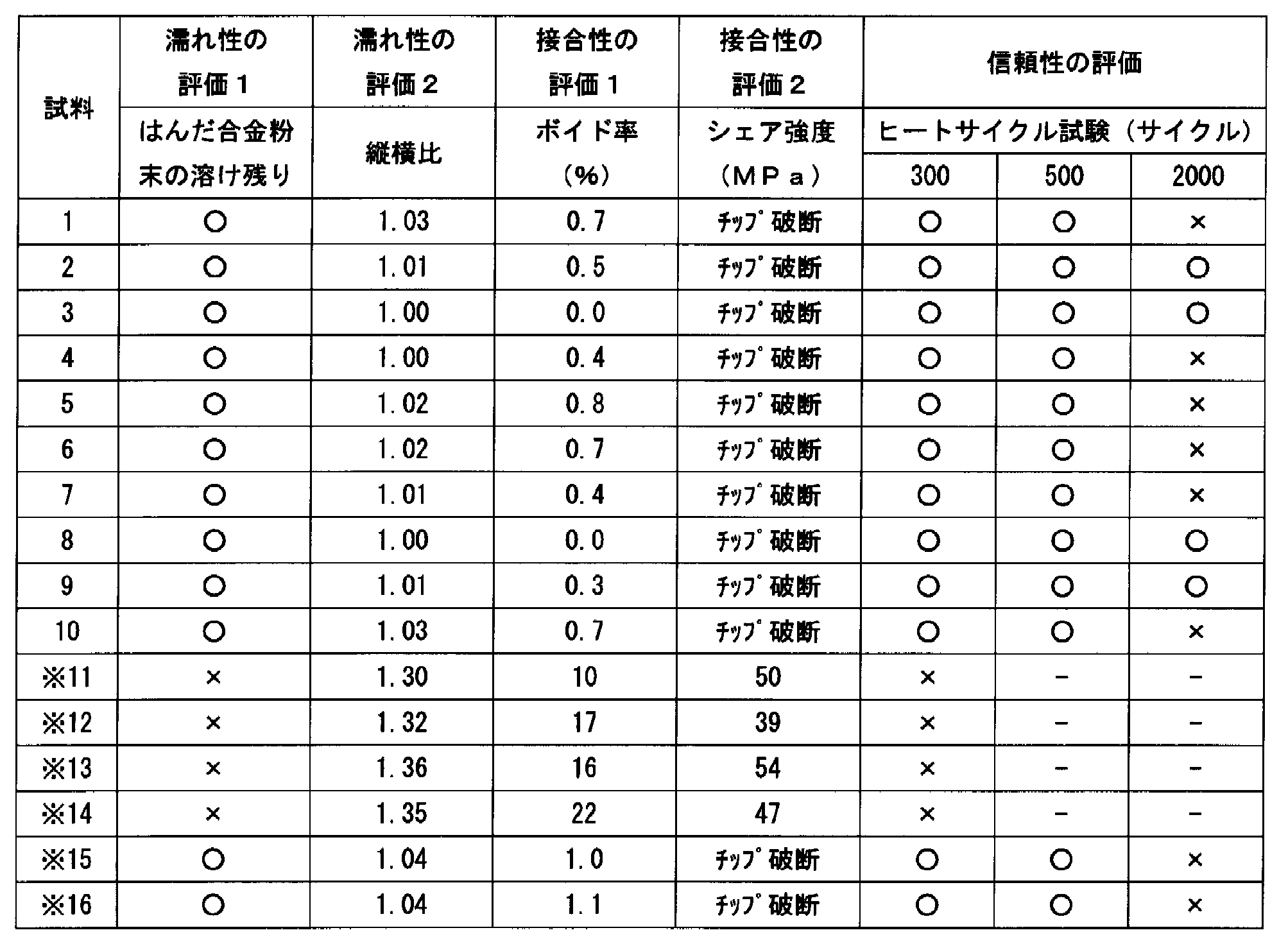
上記表2から分かるように、本発明の試料1~10のはんだ合金は、各評価項目において良好な特性を示している。即ち、濡れ性の評価1では、粉末の溶け残りは全く無かった。濡れ性の評価2では、縦横比は1.03以下で円状に均一に濡れ広がっていた。接合性の評価1では、ボイド率が0.8%以下であり非常に低い値であった。濡れ性の評価2では、シェア強度試験を行った結果、はんだ合金の強度が高く全てチップで破断し、はんだ合金中では破断しなかった。信頼性の評価では、ヒートサイクル試験で500サイクルまで不良は発生しなかった。
このように良好な結果が得られた理由は本発明のはんだ合金が適正な組成範囲内であり、はんだペーストが適切な条件で製造されたからであると言える。なお、試料3,8は、はんだ合金粉末の金属組織が90体積%以上ラメラ組織であり、各評価結果も非常に良い結果であった。このように良好な結果が得られた理由は、微細なラメラ組織の割合が90体積%以上であることからはんだ合金が均一に溶融し、各部で均一な接合が可能となり、よって高い接合信頼性など良好な結果が得られたためと考えられる。
また、Au量の多い従来製品である比較例の試料15,16は実施例同様に良好な結果が得られていることが分かる。
また、Au量の多い従来製品である比較例の試料15,16は実施例同様に良好な結果が得られていることが分かる。
一方、比較例である試料11~14の各はんだ合金は、少なくともいずれかの特性において好ましくない結果となった。即ち、試料11~14では、はんだ合金粉末溶け残りが発生し、縦横比は1.04以上であった。さらにシェア強度は39~54MPaと低く、ボイド率については10~22%程度であってボイドがかなりの割合で発生した。そして信頼性の評価であるヒートサイクル試験では全ての試料に関して300サイクルまでの間に不良が発生した。
更に本発明のはんだ合金はAu含有量が多くても61%であり、現在、実用化されている80質量%Au-20質量%合金や88質量%Au-12質量%Ge合金などよりも格段にAu含有量が少なく、よって低コストであることが分かる。
なお水晶振動子パッケージはリークしてしまうと水晶振動子の発振周波数がずれたり安定しなくなったりしてしまうため、高い接合信頼性を有する接合材料(はんだ材料)を用いる必要がある。例えば封止時にはんだ材料がずれたり、流れだしたりしてしまうと十分な接合性が得られず、またはショートしてしまったりしてしまう。ボイドが発生したりしてもファインリーク(わずかなリーク)の原因となり、不良率が増加して好ましくない。本発明のはんだペーストを用いることにより封止容器上に封止形状に沿った精度良いはんだ材料の供給が可能となり、封止容器と封止蓋を精度良く接合することができる。接合後のはんだ合金は従来のAu系はんだ合金よりも応力緩和性に優れるため接合性や信頼性等に優れる。また使用するAu量が低減できるため、低コストであって非常に高い信頼性を要求される水晶振動子パッケージの封止用としても好適なはんだ材料である。
1 Cu基板
2 Ni層
3 はんだ合金(はんだペースト)
4 Siチップ
5 水晶振動子
6 導電性接着剤
7 端子
8 封止用蓋
9 封止用容器
2 Ni層
3 はんだ合金(はんだペースト)
4 Siチップ
5 水晶振動子
6 導電性接着剤
7 端子
8 封止用蓋
9 封止用容器
Claims (7)
- はんだ合金粉末とフラックスとを混合してなるはんだペーストであって、該はんだ合金粉末はその合計を100質量%としたとき、Snを27.5質量%以上33.0質量%未満含有し、Agを8.0質量%以上14.5質量%以下含有し、残部が製造上、不可避に含まれる元素を除き、Auからなることを特徴とするPbフリーAu-Sn-Ag系はんだペースト。
- 前記フラックスがロジンを含んでいることを特徴とする、請求項1に記載のPbフリーAu-Sn-Ag系はんだペースト。
- Snを29.0質量%以上32.0質量%以下含有し、Agを10.0質量%以上14.0質量%以下含有し、残部が製造上、不可避に含まれる元素を除き、Auからなることを特徴とする請求項1又は2に記載のPbフリーAu-Sn-Ag系はんだペースト。
- はんだ合金粉末の金属組織の少なくとも一部がラメラ組織であることを特徴とする請求項1乃至3の何れかに記載のPbフリーAu-Sn-Ag系はんだペースト。
- はんだ合金粉末の金属組織がラメラ組織であり、その割合が90体積%以上であることを特徴とする請求項1乃至4の何れかに記載のPbフリーAu-Sn-Ag系はんだペースト。
- 請求項1乃至5の何れかに記載のPbフリーAu-Sn-Ag系はんだペーストを用いて接合されていることを特徴とするSi半導体素子接合体。
- 請求項1乃至5に記載のPbフリーAu-Sn-Ag系はんだペーストを用いて封止されていることを特徴とする水晶振動子封止素子。
Applications Claiming Priority (2)
| Application Number | Priority Date | Filing Date | Title |
|---|---|---|---|
| JP2015043859A JP2018069243A (ja) | 2015-03-05 | 2015-03-05 | Au−Sn−Ag系はんだペースト並びにこのAu−Sn−Ag系はんだペーストを用いて接合もしくは封止された電子部品 |
| JP2015-043859 | 2015-03-05 |
Publications (1)
| Publication Number | Publication Date |
|---|---|
| WO2016139848A1 true WO2016139848A1 (ja) | 2016-09-09 |
Family
ID=56848884
Family Applications (1)
| Application Number | Title | Priority Date | Filing Date |
|---|---|---|---|
| PCT/JP2015/082578 Ceased WO2016139848A1 (ja) | 2015-03-05 | 2015-11-19 | Au-Sn-Ag系はんだペースト並びにこのAu-Sn-Ag系はんだペーストを用いて接合もしくは封止された電子部品 |
Country Status (3)
| Country | Link |
|---|---|
| JP (1) | JP2018069243A (ja) |
| TW (1) | TW201701985A (ja) |
| WO (1) | WO2016139848A1 (ja) |
Cited By (3)
| Publication number | Priority date | Publication date | Assignee | Title |
|---|---|---|---|---|
| WO2018070336A1 (ja) * | 2016-10-14 | 2018-04-19 | 株式会社村田製作所 | 圧電振動子及び圧電発振装置並びにこれらの製造方法 |
| CN115846930A (zh) * | 2022-12-29 | 2023-03-28 | 北京康普锡威科技有限公司 | 预成型焊料组合物、焊片及制备方法 |
| CN116213996A (zh) * | 2023-01-04 | 2023-06-06 | 有研亿金新材料有限公司 | 一种具有良好点胶性能的金基合金焊膏及其制备方法 |
Citations (3)
| Publication number | Priority date | Publication date | Assignee | Title |
|---|---|---|---|---|
| JP2008155221A (ja) * | 2006-12-21 | 2008-07-10 | Seiko Epson Corp | ろう材、圧電デバイス、圧電デバイスの封止方法 |
| JP4305511B2 (ja) * | 2004-11-01 | 2009-07-29 | 千住金属工業株式会社 | 高温鉛フリーはんだおよび半導体素子収納用パッケージ |
| WO2015087588A1 (ja) * | 2013-12-10 | 2015-06-18 | 住友金属鉱山株式会社 | Au-Sn-Ag系はんだ合金並びにこのAu-Sn-Ag系はんだ合金を用いて封止された電子部品及び電子部品搭載装置 |
-
2015
- 2015-03-05 JP JP2015043859A patent/JP2018069243A/ja active Pending
- 2015-11-19 WO PCT/JP2015/082578 patent/WO2016139848A1/ja not_active Ceased
-
2016
- 2016-03-01 TW TW105106155A patent/TW201701985A/zh unknown
Patent Citations (3)
| Publication number | Priority date | Publication date | Assignee | Title |
|---|---|---|---|---|
| JP4305511B2 (ja) * | 2004-11-01 | 2009-07-29 | 千住金属工業株式会社 | 高温鉛フリーはんだおよび半導体素子収納用パッケージ |
| JP2008155221A (ja) * | 2006-12-21 | 2008-07-10 | Seiko Epson Corp | ろう材、圧電デバイス、圧電デバイスの封止方法 |
| WO2015087588A1 (ja) * | 2013-12-10 | 2015-06-18 | 住友金属鉱山株式会社 | Au-Sn-Ag系はんだ合金並びにこのAu-Sn-Ag系はんだ合金を用いて封止された電子部品及び電子部品搭載装置 |
Cited By (4)
| Publication number | Priority date | Publication date | Assignee | Title |
|---|---|---|---|---|
| WO2018070336A1 (ja) * | 2016-10-14 | 2018-04-19 | 株式会社村田製作所 | 圧電振動子及び圧電発振装置並びにこれらの製造方法 |
| CN115846930A (zh) * | 2022-12-29 | 2023-03-28 | 北京康普锡威科技有限公司 | 预成型焊料组合物、焊片及制备方法 |
| CN116213996A (zh) * | 2023-01-04 | 2023-06-06 | 有研亿金新材料有限公司 | 一种具有良好点胶性能的金基合金焊膏及其制备方法 |
| CN116213996B (zh) * | 2023-01-04 | 2025-11-07 | 有研亿金新材料有限公司 | 一种具有良好点胶性能的金基合金焊膏及其制备方法 |
Also Published As
| Publication number | Publication date |
|---|---|
| TW201701985A (zh) | 2017-01-16 |
| JP2018069243A (ja) | 2018-05-10 |
Similar Documents
| Publication | Publication Date | Title |
|---|---|---|
| CN115139009B (zh) | 预成型焊料及其制备方法、以及焊接接头的制备方法 | |
| CN106660178A (zh) | 无铅焊料合金组合物和用于制备无铅焊料合金的方法 | |
| CN105813801A (zh) | Au-Sn-Ag系焊料合金以及使用该Au-Sn-Ag系焊料合金进行密封的电子部件和电子部件搭载装置 | |
| JP6780994B2 (ja) | はんだ材料及び電子部品 | |
| JP4807465B1 (ja) | Pbフリーはんだ合金 | |
| JP5962461B2 (ja) | Au−Ge−Sn系はんだ合金 | |
| JP4560830B2 (ja) | はんだペースト用Au−Sn合金粉末 | |
| JP2016026884A (ja) | 中低温用のBi−Sn−Al系はんだ合金及びはんだペースト | |
| JP2018069243A (ja) | Au−Sn−Ag系はんだペースト並びにこのAu−Sn−Ag系はんだペーストを用いて接合もしくは封止された電子部品 | |
| JP2011251330A (ja) | 高温鉛フリーはんだペースト | |
| WO2016170906A1 (ja) | Au-Sn-Ag系はんだペースト並びにこのAu-Sn-Ag系はんだペーストを用いて接合もしくは封止された電子部品 | |
| JP2007160340A (ja) | ロウ材 | |
| JP2017170480A (ja) | 高温用Pbフリーはんだペースト及びその製造方法 | |
| JP2016068123A (ja) | Au−Sn−Ag系はんだ合金及びこれを用いて封止若しくは接合された電子機器並びに該電子機器を搭載した電子装置 | |
| JP2016059943A (ja) | ボール状Au−Ge−Sn系はんだ合金及び該はんだ合金を用いた電子部品 | |
| JP2015157307A (ja) | Au−Sn−Ag系はんだ合金並びにこのAu−Sn−Ag系はんだ合金を用いて封止された電子部品及び電子部品搭載装置 | |
| JP5979083B2 (ja) | PbフリーAu−Ge−Sn系はんだ合金 | |
| JP2015136735A (ja) | ボール状Au−Sn−Ag系はんだ合金並びにこのボール状Au−Sn−Ag系はんだ合金を用いて封止された電子部品及び電子部品搭載装置 | |
| JP2017177122A (ja) | 高温Pbフリーはんだペースト及びその製造方法 | |
| JP2015188892A (ja) | ボール状Au−Sn−Ag系はんだ合金並びにこのボール状Au−Sn−Ag系はんだ合金を用いて封止された電子部品及び電子部品搭載装置 | |
| JP2016026883A (ja) | 中低温用のBi−Sn−Zn系はんだ合金及びはんだペースト | |
| JP2016028829A (ja) | Au−Sn−Ag系はんだ合金並びにこのAu−Sn−Ag系はんだ合金を用いて封止された電子部品及び電子部品搭載装置 | |
| JP2016059924A (ja) | Au−Sn−Ag系はんだ合金並びにこのAu−Sn−Ag系はんだ合金を用いて封止された電子部品及び電子部品搭載装置 | |
| JP2017070959A (ja) | Au−Sb−Sn系はんだペースト | |
| JP2016087641A (ja) | Pbを含まないAl−Cu系はんだ合金 |
Legal Events
| Date | Code | Title | Description |
|---|---|---|---|
| 121 | Ep: the epo has been informed by wipo that ep was designated in this application |
Ref document number: 15884014 Country of ref document: EP Kind code of ref document: A1 |
|
| NENP | Non-entry into the national phase |
Ref country code: DE |
|
| NENP | Non-entry into the national phase |
Ref country code: JP |
|
| 122 | Ep: pct application non-entry in european phase |
Ref document number: 15884014 Country of ref document: EP Kind code of ref document: A1 |