WO2016136255A1 - 成膜装置及び成膜方法 - Google Patents
成膜装置及び成膜方法 Download PDFInfo
- Publication number
- WO2016136255A1 WO2016136255A1 PCT/JP2016/000989 JP2016000989W WO2016136255A1 WO 2016136255 A1 WO2016136255 A1 WO 2016136255A1 JP 2016000989 W JP2016000989 W JP 2016000989W WO 2016136255 A1 WO2016136255 A1 WO 2016136255A1
- Authority
- WO
- WIPO (PCT)
- Prior art keywords
- substrate
- deposition
- film forming
- etching
- stage
- Prior art date
- Legal status (The legal status is an assumption and is not a legal conclusion. Google has not performed a legal analysis and makes no representation as to the accuracy of the status listed.)
- Ceased
Links
Images



Classifications
-
- H—ELECTRICITY
- H10—SEMICONDUCTOR DEVICES; ELECTRIC SOLID-STATE DEVICES NOT OTHERWISE PROVIDED FOR
- H10P—GENERIC PROCESSES OR APPARATUS FOR THE MANUFACTURE OR TREATMENT OF DEVICES COVERED BY CLASS H10
- H10P14/00—Formation of materials, e.g. in the shape of layers or pillars
- H10P14/60—Formation of materials, e.g. in the shape of layers or pillars of insulating materials
- H10P14/63—Formation of materials, e.g. in the shape of layers or pillars of insulating materials characterised by the formation processes
- H10P14/6326—Deposition processes
- H10P14/6328—Deposition from the gas or vapour phase
- H10P14/6329—Deposition from the gas or vapour phase using physical ablation of a target, e.g. physical vapour deposition or pulsed laser deposition
-
- H—ELECTRICITY
- H10—SEMICONDUCTOR DEVICES; ELECTRIC SOLID-STATE DEVICES NOT OTHERWISE PROVIDED FOR
- H10W—GENERIC PACKAGES, INTERCONNECTIONS, CONNECTORS OR OTHER CONSTRUCTIONAL DETAILS OF DEVICES COVERED BY CLASS H10
- H10W20/00—Interconnections in chips, wafers or substrates
- H10W20/01—Manufacture or treatment
- H10W20/031—Manufacture or treatment of conductive parts of the interconnections
- H10W20/032—Manufacture or treatment of conductive parts of the interconnections of conductive barrier, adhesion or liner layers
- H10W20/055—Manufacture or treatment of conductive parts of the interconnections of conductive barrier, adhesion or liner layers by formation methods other than physical vapour deposition [PVD], chemical vapour deposition [CVD] or liquid deposition
-
- C—CHEMISTRY; METALLURGY
- C23—COATING METALLIC MATERIAL; COATING MATERIAL WITH METALLIC MATERIAL; CHEMICAL SURFACE TREATMENT; DIFFUSION TREATMENT OF METALLIC MATERIAL; COATING BY VACUUM EVAPORATION, BY SPUTTERING, BY ION IMPLANTATION OR BY CHEMICAL VAPOUR DEPOSITION, IN GENERAL; INHIBITING CORROSION OF METALLIC MATERIAL OR INCRUSTATION IN GENERAL
- C23C—COATING METALLIC MATERIAL; COATING MATERIAL WITH METALLIC MATERIAL; SURFACE TREATMENT OF METALLIC MATERIAL BY DIFFUSION INTO THE SURFACE, BY CHEMICAL CONVERSION OR SUBSTITUTION; COATING BY VACUUM EVAPORATION, BY SPUTTERING, BY ION IMPLANTATION OR BY CHEMICAL VAPOUR DEPOSITION, IN GENERAL
- C23C14/00—Coating by vacuum evaporation, by sputtering or by ion implantation of the coating forming material
- C23C14/04—Coating on selected surface areas, e.g. using masks
- C23C14/046—Coating cavities or hollow spaces, e.g. interior of tubes; Infiltration of porous substrates
-
- C—CHEMISTRY; METALLURGY
- C23—COATING METALLIC MATERIAL; COATING MATERIAL WITH METALLIC MATERIAL; CHEMICAL SURFACE TREATMENT; DIFFUSION TREATMENT OF METALLIC MATERIAL; COATING BY VACUUM EVAPORATION, BY SPUTTERING, BY ION IMPLANTATION OR BY CHEMICAL VAPOUR DEPOSITION, IN GENERAL; INHIBITING CORROSION OF METALLIC MATERIAL OR INCRUSTATION IN GENERAL
- C23C—COATING METALLIC MATERIAL; COATING MATERIAL WITH METALLIC MATERIAL; SURFACE TREATMENT OF METALLIC MATERIAL BY DIFFUSION INTO THE SURFACE, BY CHEMICAL CONVERSION OR SUBSTITUTION; COATING BY VACUUM EVAPORATION, BY SPUTTERING, BY ION IMPLANTATION OR BY CHEMICAL VAPOUR DEPOSITION, IN GENERAL
- C23C14/00—Coating by vacuum evaporation, by sputtering or by ion implantation of the coating forming material
- C23C14/06—Coating by vacuum evaporation, by sputtering or by ion implantation of the coating forming material characterised by the coating material
- C23C14/14—Metallic material, boron or silicon
- C23C14/16—Metallic material, boron or silicon on metallic substrates or on substrates of boron or silicon
- C23C14/165—Metallic material, boron or silicon on metallic substrates or on substrates of boron or silicon by cathodic sputtering
-
- C—CHEMISTRY; METALLURGY
- C23—COATING METALLIC MATERIAL; COATING MATERIAL WITH METALLIC MATERIAL; CHEMICAL SURFACE TREATMENT; DIFFUSION TREATMENT OF METALLIC MATERIAL; COATING BY VACUUM EVAPORATION, BY SPUTTERING, BY ION IMPLANTATION OR BY CHEMICAL VAPOUR DEPOSITION, IN GENERAL; INHIBITING CORROSION OF METALLIC MATERIAL OR INCRUSTATION IN GENERAL
- C23C—COATING METALLIC MATERIAL; COATING MATERIAL WITH METALLIC MATERIAL; SURFACE TREATMENT OF METALLIC MATERIAL BY DIFFUSION INTO THE SURFACE, BY CHEMICAL CONVERSION OR SUBSTITUTION; COATING BY VACUUM EVAPORATION, BY SPUTTERING, BY ION IMPLANTATION OR BY CHEMICAL VAPOUR DEPOSITION, IN GENERAL
- C23C14/00—Coating by vacuum evaporation, by sputtering or by ion implantation of the coating forming material
- C23C14/06—Coating by vacuum evaporation, by sputtering or by ion implantation of the coating forming material characterised by the coating material
- C23C14/14—Metallic material, boron or silicon
- C23C14/18—Metallic material, boron or silicon on other inorganic substrates
- C23C14/185—Metallic material, boron or silicon on other inorganic substrates by cathodic sputtering
-
- C—CHEMISTRY; METALLURGY
- C23—COATING METALLIC MATERIAL; COATING MATERIAL WITH METALLIC MATERIAL; CHEMICAL SURFACE TREATMENT; DIFFUSION TREATMENT OF METALLIC MATERIAL; COATING BY VACUUM EVAPORATION, BY SPUTTERING, BY ION IMPLANTATION OR BY CHEMICAL VAPOUR DEPOSITION, IN GENERAL; INHIBITING CORROSION OF METALLIC MATERIAL OR INCRUSTATION IN GENERAL
- C23C—COATING METALLIC MATERIAL; COATING MATERIAL WITH METALLIC MATERIAL; SURFACE TREATMENT OF METALLIC MATERIAL BY DIFFUSION INTO THE SURFACE, BY CHEMICAL CONVERSION OR SUBSTITUTION; COATING BY VACUUM EVAPORATION, BY SPUTTERING, BY ION IMPLANTATION OR BY CHEMICAL VAPOUR DEPOSITION, IN GENERAL
- C23C14/00—Coating by vacuum evaporation, by sputtering or by ion implantation of the coating forming material
- C23C14/22—Coating by vacuum evaporation, by sputtering or by ion implantation of the coating forming material characterised by the process of coating
- C23C14/34—Sputtering
- C23C14/3407—Cathode assembly for sputtering apparatus, e.g. Target
-
- C—CHEMISTRY; METALLURGY
- C23—COATING METALLIC MATERIAL; COATING MATERIAL WITH METALLIC MATERIAL; CHEMICAL SURFACE TREATMENT; DIFFUSION TREATMENT OF METALLIC MATERIAL; COATING BY VACUUM EVAPORATION, BY SPUTTERING, BY ION IMPLANTATION OR BY CHEMICAL VAPOUR DEPOSITION, IN GENERAL; INHIBITING CORROSION OF METALLIC MATERIAL OR INCRUSTATION IN GENERAL
- C23C—COATING METALLIC MATERIAL; COATING MATERIAL WITH METALLIC MATERIAL; SURFACE TREATMENT OF METALLIC MATERIAL BY DIFFUSION INTO THE SURFACE, BY CHEMICAL CONVERSION OR SUBSTITUTION; COATING BY VACUUM EVAPORATION, BY SPUTTERING, BY ION IMPLANTATION OR BY CHEMICAL VAPOUR DEPOSITION, IN GENERAL
- C23C14/00—Coating by vacuum evaporation, by sputtering or by ion implantation of the coating forming material
- C23C14/58—After-treatment
-
- C—CHEMISTRY; METALLURGY
- C23—COATING METALLIC MATERIAL; COATING MATERIAL WITH METALLIC MATERIAL; CHEMICAL SURFACE TREATMENT; DIFFUSION TREATMENT OF METALLIC MATERIAL; COATING BY VACUUM EVAPORATION, BY SPUTTERING, BY ION IMPLANTATION OR BY CHEMICAL VAPOUR DEPOSITION, IN GENERAL; INHIBITING CORROSION OF METALLIC MATERIAL OR INCRUSTATION IN GENERAL
- C23C—COATING METALLIC MATERIAL; COATING MATERIAL WITH METALLIC MATERIAL; SURFACE TREATMENT OF METALLIC MATERIAL BY DIFFUSION INTO THE SURFACE, BY CHEMICAL CONVERSION OR SUBSTITUTION; COATING BY VACUUM EVAPORATION, BY SPUTTERING, BY ION IMPLANTATION OR BY CHEMICAL VAPOUR DEPOSITION, IN GENERAL
- C23C14/00—Coating by vacuum evaporation, by sputtering or by ion implantation of the coating forming material
- C23C14/58—After-treatment
- C23C14/5826—Treatment with charged particles
-
- H—ELECTRICITY
- H01—ELECTRIC ELEMENTS
- H01J—ELECTRIC DISCHARGE TUBES OR DISCHARGE LAMPS
- H01J37/00—Discharge tubes with provision for introducing objects or material to be exposed to the discharge, e.g. for the purpose of examination or processing thereof
- H01J37/32—Gas-filled discharge tubes
- H01J37/32009—Arrangements for generation of plasma specially adapted for examination or treatment of objects, e.g. plasma sources
- H01J37/32018—Glow discharge
- H01J37/32036—AC powered
-
- H—ELECTRICITY
- H01—ELECTRIC ELEMENTS
- H01J—ELECTRIC DISCHARGE TUBES OR DISCHARGE LAMPS
- H01J37/00—Discharge tubes with provision for introducing objects or material to be exposed to the discharge, e.g. for the purpose of examination or processing thereof
- H01J37/32—Gas-filled discharge tubes
- H01J37/32009—Arrangements for generation of plasma specially adapted for examination or treatment of objects, e.g. plasma sources
- H01J37/32366—Localised processing
-
- H—ELECTRICITY
- H01—ELECTRIC ELEMENTS
- H01J—ELECTRIC DISCHARGE TUBES OR DISCHARGE LAMPS
- H01J37/00—Discharge tubes with provision for introducing objects or material to be exposed to the discharge, e.g. for the purpose of examination or processing thereof
- H01J37/32—Gas-filled discharge tubes
- H01J37/32009—Arrangements for generation of plasma specially adapted for examination or treatment of objects, e.g. plasma sources
- H01J37/32403—Treating multiple sides of workpieces, e.g. 3D workpieces
-
- H—ELECTRICITY
- H01—ELECTRIC ELEMENTS
- H01J—ELECTRIC DISCHARGE TUBES OR DISCHARGE LAMPS
- H01J37/00—Discharge tubes with provision for introducing objects or material to be exposed to the discharge, e.g. for the purpose of examination or processing thereof
- H01J37/32—Gas-filled discharge tubes
- H01J37/32431—Constructional details of the reactor
- H01J37/32458—Vessel
- H01J37/32477—Vessel characterised by the means for protecting vessels or internal parts, e.g. coatings
-
- H—ELECTRICITY
- H01—ELECTRIC ELEMENTS
- H01J—ELECTRIC DISCHARGE TUBES OR DISCHARGE LAMPS
- H01J37/00—Discharge tubes with provision for introducing objects or material to be exposed to the discharge, e.g. for the purpose of examination or processing thereof
- H01J37/32—Gas-filled discharge tubes
- H01J37/32431—Constructional details of the reactor
- H01J37/32458—Vessel
- H01J37/32513—Sealing means, e.g. sealing between different parts of the vessel
-
- H—ELECTRICITY
- H01—ELECTRIC ELEMENTS
- H01J—ELECTRIC DISCHARGE TUBES OR DISCHARGE LAMPS
- H01J37/00—Discharge tubes with provision for introducing objects or material to be exposed to the discharge, e.g. for the purpose of examination or processing thereof
- H01J37/32—Gas-filled discharge tubes
- H01J37/32431—Constructional details of the reactor
- H01J37/32623—Mechanical discharge control means
-
- H—ELECTRICITY
- H01—ELECTRIC ELEMENTS
- H01J—ELECTRIC DISCHARGE TUBES OR DISCHARGE LAMPS
- H01J37/00—Discharge tubes with provision for introducing objects or material to be exposed to the discharge, e.g. for the purpose of examination or processing thereof
- H01J37/32—Gas-filled discharge tubes
- H01J37/34—Gas-filled discharge tubes operating with cathodic sputtering
- H01J37/3402—Gas-filled discharge tubes operating with cathodic sputtering using supplementary magnetic fields
- H01J37/3405—Magnetron sputtering
- H01J37/3408—Planar magnetron sputtering
-
- H—ELECTRICITY
- H01—ELECTRIC ELEMENTS
- H01J—ELECTRIC DISCHARGE TUBES OR DISCHARGE LAMPS
- H01J37/00—Discharge tubes with provision for introducing objects or material to be exposed to the discharge, e.g. for the purpose of examination or processing thereof
- H01J37/32—Gas-filled discharge tubes
- H01J37/34—Gas-filled discharge tubes operating with cathodic sputtering
- H01J37/3411—Constructional aspects of the reactor
- H01J37/3414—Targets
- H01J37/3426—Material
-
- H—ELECTRICITY
- H01—ELECTRIC ELEMENTS
- H01J—ELECTRIC DISCHARGE TUBES OR DISCHARGE LAMPS
- H01J37/00—Discharge tubes with provision for introducing objects or material to be exposed to the discharge, e.g. for the purpose of examination or processing thereof
- H01J37/32—Gas-filled discharge tubes
- H01J37/34—Gas-filled discharge tubes operating with cathodic sputtering
- H01J37/3476—Testing and control
-
- H—ELECTRICITY
- H10—SEMICONDUCTOR DEVICES; ELECTRIC SOLID-STATE DEVICES NOT OTHERWISE PROVIDED FOR
- H10P—GENERIC PROCESSES OR APPARATUS FOR THE MANUFACTURE OR TREATMENT OF DEVICES COVERED BY CLASS H10
- H10P14/00—Formation of materials, e.g. in the shape of layers or pillars
- H10P14/40—Formation of materials, e.g. in the shape of layers or pillars of conductive or resistive materials
- H10P14/42—Formation of materials, e.g. in the shape of layers or pillars of conductive or resistive materials using a gas or vapour
-
- H—ELECTRICITY
- H10—SEMICONDUCTOR DEVICES; ELECTRIC SOLID-STATE DEVICES NOT OTHERWISE PROVIDED FOR
- H10P—GENERIC PROCESSES OR APPARATUS FOR THE MANUFACTURE OR TREATMENT OF DEVICES COVERED BY CLASS H10
- H10P14/00—Formation of materials, e.g. in the shape of layers or pillars
- H10P14/40—Formation of materials, e.g. in the shape of layers or pillars of conductive or resistive materials
- H10P14/42—Formation of materials, e.g. in the shape of layers or pillars of conductive or resistive materials using a gas or vapour
- H10P14/44—Physical vapour deposition [PVD]
-
- H—ELECTRICITY
- H10—SEMICONDUCTOR DEVICES; ELECTRIC SOLID-STATE DEVICES NOT OTHERWISE PROVIDED FOR
- H10P—GENERIC PROCESSES OR APPARATUS FOR THE MANUFACTURE OR TREATMENT OF DEVICES COVERED BY CLASS H10
- H10P50/00—Etching of wafers, substrates or parts of devices
- H10P50/20—Dry etching; Plasma etching; Reactive-ion etching
- H10P50/24—Dry etching; Plasma etching; Reactive-ion etching of semiconductor materials
- H10P50/242—Dry etching; Plasma etching; Reactive-ion etching of semiconductor materials of Group IV materials
-
- H—ELECTRICITY
- H10—SEMICONDUCTOR DEVICES; ELECTRIC SOLID-STATE DEVICES NOT OTHERWISE PROVIDED FOR
- H10W—GENERIC PACKAGES, INTERCONNECTIONS, CONNECTORS OR OTHER CONSTRUCTIONAL DETAILS OF DEVICES COVERED BY CLASS H10
- H10W20/00—Interconnections in chips, wafers or substrates
- H10W20/01—Manufacture or treatment
- H10W20/031—Manufacture or treatment of conductive parts of the interconnections
- H10W20/032—Manufacture or treatment of conductive parts of the interconnections of conductive barrier, adhesion or liner layers
- H10W20/033—Manufacture or treatment of conductive parts of the interconnections of conductive barrier, adhesion or liner layers in openings in dielectrics
-
- H—ELECTRICITY
- H10—SEMICONDUCTOR DEVICES; ELECTRIC SOLID-STATE DEVICES NOT OTHERWISE PROVIDED FOR
- H10W—GENERIC PACKAGES, INTERCONNECTIONS, CONNECTORS OR OTHER CONSTRUCTIONAL DETAILS OF DEVICES COVERED BY CLASS H10
- H10W20/00—Interconnections in chips, wafers or substrates
- H10W20/01—Manufacture or treatment
- H10W20/031—Manufacture or treatment of conductive parts of the interconnections
- H10W20/032—Manufacture or treatment of conductive parts of the interconnections of conductive barrier, adhesion or liner layers
- H10W20/054—Manufacture or treatment of conductive parts of the interconnections of conductive barrier, adhesion or liner layers by selectively removing parts thereof
-
- H—ELECTRICITY
- H01—ELECTRIC ELEMENTS
- H01J—ELECTRIC DISCHARGE TUBES OR DISCHARGE LAMPS
- H01J2237/00—Discharge tubes exposing object to beam, e.g. for analysis treatment, etching, imaging
- H01J2237/32—Processing objects by plasma generation
- H01J2237/33—Processing objects by plasma generation characterised by the type of processing
- H01J2237/334—Etching
Definitions
- the present invention relates to a film forming apparatus and a film forming method, and more particularly to an apparatus suitable for forming a thin film with good coverage on the inner surface of a fine hole having a high aspect ratio.
- the semiconductor device manufacturing process includes a process of forming a barrier layer made of a Ta film on the inner surface (inner wall surface and bottom surface) of a via hole or contact hole having a predetermined aspect ratio.
- a barrier layer made of a Ta film on the inner surface (inner wall surface and bottom surface) of a via hole or contact hole having a predetermined aspect ratio.
- Patent Document 1 discloses an apparatus that can perform an etching process for etching a film. According to this, the Ta film formed thickly on the substrate surface and the bottom of the hole by the film forming process is etched, and the etched Ta particles adhere to the inner wall surface of the thin hole, thereby improving the coverage.
- the vacuum chamber in order to prevent the sputter particles from adhering to the inner wall of the vacuum chamber and the components existing in the vacuum chamber, the vacuum chamber is protected so as to surround the space between the target and the substrate.
- a landing plate is arranged.
- positioned around a stage is a board
- the etching process is performed in such a state where the adhesion preventing plate is arranged, the in-plane distribution of the etching rate is deteriorated and the coverage cannot be sufficiently improved.
- the inventor of the present invention has made extensive studies, and the deterioration of the in-plane distribution of the etching rate is caused by the negative charges accumulated in the substrate being attracted to the portion of the deposition preventing plate adjacent to the substrate and concentrated on the edge portion of the substrate. The knowledge that it originates in was obtained.
- the present invention provides a film forming apparatus and a film forming method capable of forming a thin film with good coverage on the inner surface of a hole with a high aspect ratio by preventing negative charges from concentrating on the edge portion of the substrate during the etching process.
- the issue is to provide.
- a vacuum chamber in which a target is disposed, a stage for holding a substrate in the vacuum chamber, a first power source for supplying predetermined power to the target, and a second power for supplying AC power to the stage And a film forming process for sputtering the target by applying power to the target from the first power supply, and an etching process for etching the thin film formed on the substrate by applying AC power to the stage by the second power supply.
- the deposition plate is arranged around the substrate, the deposition surface side of the substrate held by the stage is up, and the portion of the deposition plate close to the substrate is equivalent to the substrate top surface It is characterized by comprising drive means for moving the shield up and down between a film forming position located on a plane and an etching position where the part of the deposition preventing plate is located above the upper surface of the substrate.
- the adhesion plate when etching is performed after the film forming process, the adhesion plate is moved to the etching position by the driving means, and the portion of the deposition plate that is close to the substrate is separated from the substrate. Concentration of charges can be prevented and the in-plane distribution of the etching rate can be improved. Therefore, if the present invention is applied when forming a thin film in a hole with a high aspect ratio, the thin film can be formed on the inner surface of the hole with good coverage.
- the height of the protrusion can be set to be equal to or greater than the distance between the film forming position and the etching position, and can be set to a range of 10 to 30 mm, for example.
- a second deposition plate disposed below the deposition plate, a film formation position where the upper end of the second deposition plate is located below the substrate, and this You may comprise further the 2nd drive means which moves a 2nd adhesion prevention board up and down between the etching positions near the board
- a pair of upper and lower coils are provided in the vacuum chamber, and the pair of upper and lower coils are positioned with respect to the vacuum chamber so as to sandwich the plasma generated when AC power is applied to the stage by the second power source in the vertical direction.
- a substrate is held by a stage in a vacuum chamber, a deposition plate is disposed so as to surround the stage, and sputtering is performed by applying predetermined power to a target in the vacuum chamber.
- the film forming method of the present invention which includes a film forming process and an etching process for stopping the power supply to the target and supplying AC power to the stage to etch the thin film formed on the substrate, is held by the stage.
- the deposition process is performed by moving the deposition plate to a deposition position where the deposition surface side of the substrate is on the upper side and the portion of the deposition plate that is close to the substrate in the deposition process is located on a plane equivalent to the upper surface of the substrate.
- the deposition plate is moved to an etching position different from the deposition position, where the deposition plate portion is located above the upper surface of the substrate.
- the etching position is preferably located 10 to 30 mm above the film formation position.
- a second deposition plate is disposed below the upper surface of the substrate in the film formation step, the second deposition plate is moved upward in the etching step, and scattered from the thin film in the etching step. It is preferable to prevent the particles from adhering to the inner surface of the vacuum chamber by passing between a portion adjacent to the substrate of the deposition preventing plate and the substrate.
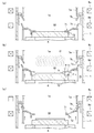
- the typical sectional view showing the sputtering device of the embodiment of the present invention is a film-forming position of an adhesion prevention board, (b) is an etching position of an adhesion prevention board, (c) is a schematic diagram which shows the conveyance position of an adhesion prevention board, respectively.
- (A) is a schematic diagram explaining a film-forming process, (b) is an etching process, respectively.
- a substrate W to be processed is formed with an insulating film L having a predetermined thickness on the surface of the silicon wafer SW, and fine holes h having an aspect ratio of 3 or more are formed in the insulating film L.
- the film forming apparatus according to the embodiment of the present invention will be described by taking as an example a sputtering apparatus that is used to form a barrier layer composed of the Ta film f on the inner surface of the hole h.
- SM is a magnetron type sputtering apparatus, and this sputtering apparatus SM includes a vacuum chamber 1 that defines a processing chamber 1a.
- a cathode unit C is attached to the ceiling of the vacuum chamber 1.
- the direction facing the ceiling portion side of the vacuum chamber 1 is referred to as “up” and the direction facing the bottom portion side is described as “down”.
- the cathode unit C includes a target assembly 2 and a magnet unit 3 disposed above the target assembly 2.
- the target assembly 2 includes a Ta target 21 formed in a circular plate shape in plan view by a known method according to the outline of the substrate W, and a bonding material (not shown) such as indium on the upper surface of the target 21.
- the target 21 can be cooled by flowing a coolant (cooling water) through the inside of the backing plate 22 during film formation by sputtering. With the target 21 mounted, the peripheral edge of the lower surface of the backing plate 22 is attached to the upper part of the side wall of the vacuum chamber 1 via the insulator I.
- An output from a first power source E1 such as a DC power source or a high frequency power source is connected to the target 21, and power having a negative potential is input to the target 21 during the film forming process.
- the magnet unit 3 generates a magnetic field in the space below the sputtering surface 21a of the target 21, captures electrons etc. ionized below the sputtering surface 21a during sputtering, and efficiently ionizes the sputtered particles scattered from the target 21. Since it has a structure, detailed description is omitted here.
- the stage 4 is disposed at the bottom of the vacuum chamber 1 so as to face the sputter surface 21a of the target 21, and the substrate W is positioned and held with its film formation surface facing upward.
- the distance between the target 21 and the substrate W is set in a range of 300 to 600 mm in consideration of productivity, the number of scattering times, and the like.
- An output from a second power source E2 such as a high frequency power source is connected to the stage 4, and AC power is input to the stage 4 during the etching process. AC power may be supplied from the second power source E2 to the stage 4 during the film forming process.
- a gas pipe 5 for introducing a sputtering gas which is a rare gas such as argon or an etching gas is connected to the side wall of the vacuum chamber 1, and a mass flow controller 51 is interposed in the gas pipe 5 so that a gas source (not shown) is connected. Communicate. Thereby, the sputter gas or etching gas whose flow rate is controlled can be introduced into the processing chamber 1a that is evacuated at a constant evacuation speed by the vacuum evacuation means 61 described later, and during the film forming process or the etching process, The pressure 1a (total pressure) is kept substantially constant.
- an exhaust pipe 6 communicating with a vacuum exhaust means 61 such as a turbo molecular pump or a rotary pump.
- an adhesion prevention plate is provided so as to surround a space between the target 21 and the substrate W in order to prevent adhesion of sputtered particles to the inner wall of the vacuum chamber 1 and parts existing in the vacuum chamber 1.
- 7a, 7b, 7c are arranged.
- a driving shaft 81 of the driving unit 8 that passes through the bottom plate of the vacuum chamber 1 is connected to the deposition preventing plate 7c that surrounds the stage 4 through a sealing unit (not shown).
- the drive means 8 since what has a well-known structure, such as an air cylinder, can be used, detailed description is abbreviate
- the portion 71 of the deposition preventing plate 7c adjacent to the substrate W is positioned on a plane equivalent to the upper surface of the substrate W, and a gap between the portion 71 and the substrate W is formed during the film forming process. The sputter particles are prevented from getting around.
- the portion 71 of the deposition preventing plate 7c is located above the upper surface of the substrate W. When an etching process is performed at this etching position, the etched particles (particles scattered from the thin film) have a space 1b between the deposition preventing plate 7c and the vacuum chamber 1 through a gap between the portion 71 and the substrate W.
- the particles may adhere to the inner surface of the vacuum chamber 1.
- the particles can be attached to the protrusions 72.
- the particles wrap around the space 1b. It is possible to prevent the adhesion to the inner surface of the vacuum chamber 1.
- the horizontal distance a from the portion 71 of the deposition preventing plate 7c at this etching position to the substrate W is preferably set in the range of 5 to 10 mm, and the vertical distance b is set in the range of 10 to 30 mm. By setting within this range, it is possible to prevent the negative charges accumulated in the substrate W from being attracted to the portion 71 during the etching process.
- the driving means 8 can move the deposition preventing plate 7c to the transport position shown in FIG. 2C when transporting the substrate W to the stage 4, and at this transport position, the portion 71 of the deposition preventing plate 7c. Is located further above the etching position.
- the vacuum chamber 1 is provided with a pair of upper and lower coils 9u and 9d, and the coil 9 is connected to an output from the power source E3.
- the coil 9 When the coil 9 is energized, an upward magnetic field can be generated in the vacuum chamber 1.
- the coils 9u and 9d are positioned with respect to the vacuum chamber 1 so as to sandwich the plasma P generated when the AC power is supplied to the stage 4 by the second power source E2 in the vertical direction. ing.
- the sputtering apparatus SM has known control means including a microcomputer, a sequencer, and the like.
- the control means operates the power supplies E1, E2, E3, the mass flow controller 51, and the vacuum exhaust means 61.
- the operation and the operation of the driving means 8 are integrated and managed.
- a film forming method for forming the Ta film f on the inner surface of the hole h of the substrate W using the sputtering apparatus SM will be described with reference to FIG.
- the driving means 8 is driven to raise the adhesion-preventing plate 7c to the transport position shown in FIG. 2C, and then the substrate W is set on the stage 4 in the vacuum chamber 1.
- the vacuum evacuation means 61 is operated to evacuate the inside of the processing chamber 1a to a predetermined degree of vacuum (for example, 1 ⁇ 10 ⁇ 5 Pa), and the driving means 8 is driven to attach the deposition preventing plate 7c to FIG. 2 (a).
- the film is lowered to the film forming position shown in FIG.
- the mass flow controller 51 is controlled to introduce argon gas at a predetermined flow rate (for example, 5 to 100 sccm) (at this time, the pressure in the processing chamber 1a is 0.04 to 0.
- the Ta film f is formed by sputtering the sputtering surface 21a of the target 21 and depositing and depositing the sputtered particles on the surface of the substrate W.
- the film thickness of the Ta film f formed on the surface of the substrate W (the upper surface of the insulating film L) and the bottom surface of the hole h is the same as that of the Ta film f formed on the inner wall surface of the hole h. It becomes thicker than the film thickness.
- the power supply from the first power supply E1 is stopped, and the driving means 8 is driven to raise the deposition preventing plate 7c to the etching position shown in FIG.
- 600 to 1200 W of AC power of 13.56 MHz is input from the second power source E2 to form plasma.
- the argon gas flow rate can be set to, for example, 50 to 100 sccm (at this time, the pressure in the processing chamber 1a is in the range of 0.4 to 0.8 Pa).
- the thick Ta film f is etched, and the etched Ta particles are reattached to the inner wall surface of the thin hole h.
- the deposition unit 7c is moved to an etching position higher than the film formation position by the driving unit 8 so that the portion 71 of the deposition plate 7c is moved to the substrate W. Therefore, the negative charges can be prevented from concentrating on the edge portion of the substrate W during the etching process, and the in-plane distribution of the etching rate can be improved. Thereby, the Ta film f can be formed on the inner surface of the high aspect ratio hole h with good coverage.
- the embodiments of the present invention have been described above, but the present invention is not limited to the above.
- the coils 9u and 9d are not energized during the etching process, but the coils 9u and 9d may be energized during the etching process. This is advantageous in that the in-plane uniformity of the etching rate can be improved as compared with the case where the coils 9u and 9d are not energized.
- the present invention is widely applied to the case where a thin film made of a metal or a metal compound other than the Ta film is formed. it can.
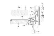
- the ridge 72 is provided on the portion 71 of the deposition preventing plate 7c adjacent to the substrate W.
- the ridge may be formed of a separate member.
- an adhesion preventing plate 7d is further provided below the adhesion preventing plate 7c, the drive shaft 11 of the second drive means 10 is connected to the adhesion preventing plate 7d, and the drive shaft 11 is driven.
- the deposition preventing plate 7d may be moved up and down between an etching position indicated by a solid line in the drawing and a film forming position (and a transfer position) indicated by a one-dot chain line in the drawing.
- the following experiment was performed using the sputtering apparatus SM.
- a substrate having a Ta film formed with a thickness of 50 nm on the surface of a Si substrate with a ⁇ 300 mm thermal oxide film was used as the substrate W.
- the deposition plate 7c was moved to the etching position to etch the Ta film.
- the distance a shown in FIG. 2B was set to 5 mm, and the distance b was set to 18 mm.
- the etching conditions in this case are as follows.
- the flow rate of the etching gas is set to 90 sccm (the pressure in the processing chamber 1a at this time is about 0.7 Pa), the input power to the stage 4 is set to 13.56 MHz and 1200 W, and the coil 9 is not energized ( Current 0A).
- the result of measuring the distribution of the etching rate at this time is indicated by a broken line L1 in FIG.
- FIG. 5 shows the result of etching under the same conditions as described above except that a current of 15 A is passed through the coil 9 as a one-dot chain line L2 and, as a conventional example, the deposition plate 7c is positioned at the film forming position.
- a solid line L3 The result when etching is performed under the same conditions as described above except for the above is indicated by a solid line L3. According to this, it was confirmed that the etching rate at the edge portion of the substrate increases when the deposition preventing plate 7c is positioned at the film forming position as in the conventional example, but the deposition preventing plate 7c is moved to the etching position. As shown by the broken line L1, the etching rate at the edge portion of the substrate can be suppressed to improve in-plane uniformity. Further, when the coil 9 is energized, the etching rate at the center of the substrate becomes as shown by the alternate long and short dash line L2. It was confirmed that the in-plane uniformity can be further improved by lowering.
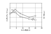
- the etching rate was measured by changing the current flowing through the coil 9 under the above etching conditions as 0A, 4A, 8A, 15A, and 20A.
- the distance between the substrate W and the target 21 was set to 600 mm
- the distance between the substrate W and the coil 9d was set to 82.5 mm
- the distance between the coil 9d and the coil 9u was set to 86 mm.
- the measurement result of the etching rate at this time is shown in FIG. According to this, it was confirmed that the in-plane uniformity of the etching rate can be improved by setting the coil current in the range of 5A to 15A.
- E1 ... first power supply
- E2 ... second power supply
- SM sputtering apparatus
- W ... substrate
- 1 ... vacuum chamber
- 4 ... stage
- 7c ... attachment plate
- 7d ... attachment plate (second prevention) Plate
- 71 Part of the deposition preventing plate 7 c adjacent to the substrate, 72... Ridge, 8... Driving means, 21.
Landscapes
- Chemical & Material Sciences (AREA)
- Engineering & Computer Science (AREA)
- Physics & Mathematics (AREA)
- Plasma & Fusion (AREA)
- Analytical Chemistry (AREA)
- Materials Engineering (AREA)
- Chemical Kinetics & Catalysis (AREA)
- Mechanical Engineering (AREA)
- Metallurgy (AREA)
- Organic Chemistry (AREA)
- Inorganic Chemistry (AREA)
- Power Engineering (AREA)
- Physical Vapour Deposition (AREA)
- Electrodes Of Semiconductors (AREA)
- Plasma Technology (AREA)
- Drying Of Semiconductors (AREA)
- Internal Circuitry In Semiconductor Integrated Circuit Devices (AREA)
- Optics & Photonics (AREA)
- Physical Deposition Of Substances That Are Components Of Semiconductor Devices (AREA)
Abstract
Description
Claims (9)
- ターゲットが配置される真空チャンバと、真空チャンバ内で基板を保持するステージと、ターゲットに所定の電力を投入する第1電源と、ステージに交流電力を投入する第2電源とを備え、第1電源によりターゲットに電力投入してターゲットをスパッタリングする成膜処理と、第2電源によりステージに交流電力を投入して基板に成膜された薄膜をエッチングするエッチング処理とを行う成膜装置であって、ステージの周囲を囲う防着板が配置されるものにおいて、
ステージで保持される基板の成膜面側を上とし、基板に近接する防着板の部分が基板上面と同等の平面上に位置する成膜位置と、この防着板の部分が基板上面から上方に位置する エッチング位置との間で防着板を上下動する駆動手段を備えることを特徴とする成膜装置。 - 前記防着板の基板に近接する部分に、下方にのびる突条を設けたことを特徴とする請求項1記載の成膜装置。
- 前記突条の高さは、前記成膜位置と前記エッチング位置との間の距離と同等以上に設定されることを特徴とする請求項2記載の成膜装置。
- 前記突条の高さは10~30mmの範囲に設定されることを特徴とする請求項2または請求項3記載の成膜装置。
- 前記防着板の下方に配置される第2防着板と、第2防着板の上端部が基板よりも下方に位置する成膜位置と、この上端部がエッチング位置に移動した前記防着板の基板に近接するエッチング位置との間で第2防着板を上下動する第2駆動手段とを更に備えることを特徴とする請求項1記載の成膜装置。
- 真空チャンバに上下一対のコイルが設けられ、第2電源によりステージに交流電力を投入したときに発生するプラズマを上下方向で挟むように真空チャンバに対して上下一対のコイルが位置決めされていることを特徴とする請求項1~5のいずれか1項記載の成膜装置。
- 真空チャンバ内のステージにより基板を保持し、ステージの周囲を囲うように防着板を配置し、真空チャンバ内のターゲットに所定の電力を投入してスパッタリングする成膜工程と、ターゲットへの電力投入を停止し、ステージに交流電力を投入して基板に成膜された薄膜をエッチングするエッチング工程とを含む成膜方法において、
ステージで保持される基板の成膜面側を上とし、前記成膜工程にて基板に近接する防着板の部分が基板上面と同等の平面上に位置する成膜位置に防着板を移動させ、前記エッチング工程にてこの防着板の部分が基板上面から上方に位置する、成膜位置とは異なるエッチング位置に防着板を移動させることを特徴とする成膜方法。 - 前記エッチング位置は前記成膜位置よりも10~30mm上方に位置することを特徴とする請求項7記載の成膜方法。
- 前記成膜工程にて基板上面よりも下方に第2防着板が配置され、前記エッチング工程にて前記第2防着板を上方に移動させ、前記エッチング工程で薄膜から飛散する粒子が、前記防着板の基板に近接する部分と基板との間を通過して真空チャンバ内面に付着することを防止するようにしたことを特徴とする請求項7または8記載の成膜方法。
Priority Applications (4)
| Application Number | Priority Date | Filing Date | Title |
|---|---|---|---|
| KR1020177006966A KR101926677B1 (ko) | 2015-02-25 | 2016-02-24 | 성막 장치 및 성막 방법 |
| CN201680001052.8A CN107408504B (zh) | 2015-02-25 | 2016-02-24 | 成膜装置及成膜方法 |
| US15/125,726 US20170004995A1 (en) | 2015-02-25 | 2016-02-24 | Film Forming Apparatus and Film Forming Method |
| JP2016556907A JP6171108B2 (ja) | 2015-02-25 | 2016-02-24 | 成膜装置及び成膜方法 |
Applications Claiming Priority (2)
| Application Number | Priority Date | Filing Date | Title |
|---|---|---|---|
| JP2015-034740 | 2015-02-25 | ||
| JP2015034740 | 2015-02-25 |
Publications (1)
| Publication Number | Publication Date |
|---|---|
| WO2016136255A1 true WO2016136255A1 (ja) | 2016-09-01 |
Family
ID=56788426
Family Applications (1)
| Application Number | Title | Priority Date | Filing Date |
|---|---|---|---|
| PCT/JP2016/000989 Ceased WO2016136255A1 (ja) | 2015-02-25 | 2016-02-24 | 成膜装置及び成膜方法 |
Country Status (6)
| Country | Link |
|---|---|
| US (1) | US20170004995A1 (ja) |
| JP (1) | JP6171108B2 (ja) |
| KR (1) | KR101926677B1 (ja) |
| CN (1) | CN107408504B (ja) |
| TW (1) | TWI599669B (ja) |
| WO (1) | WO2016136255A1 (ja) |
Cited By (3)
| Publication number | Priority date | Publication date | Assignee | Title |
|---|---|---|---|---|
| WO2018207577A1 (ja) * | 2017-05-09 | 2018-11-15 | 富士フイルム株式会社 | 成膜装置および圧電膜の成膜方法 |
| JP2021188113A (ja) * | 2020-06-05 | 2021-12-13 | 株式会社アルバック | プラズマ処理装置 |
| JP2024014724A (ja) * | 2022-07-21 | 2024-02-01 | エスケー エンパルス カンパニー リミテッド | フォーカスリング及びこれを含むプラズマエッチング装置 |
Families Citing this family (6)
| Publication number | Priority date | Publication date | Assignee | Title |
|---|---|---|---|---|
| JP7594852B2 (ja) | 2018-10-11 | 2024-12-05 | 日本発條株式会社 | ステージ、成膜装置、および膜加工装置 |
| JP7057442B2 (ja) * | 2018-11-16 | 2022-04-19 | 株式会社アルバック | 真空処理装置 |
| JP7060633B2 (ja) * | 2020-01-29 | 2022-04-26 | キヤノントッキ株式会社 | 成膜装置及び電子デバイス製造装置 |
| JP7239549B2 (ja) * | 2020-12-10 | 2023-03-14 | キヤノントッキ株式会社 | 成膜装置、成膜方法及び電子デバイスの製造方法 |
| CN112981334B (zh) * | 2021-02-05 | 2022-09-16 | 北京北方华创微电子装备有限公司 | 半导体加工设备及对半导体加工设备进行清理的工艺 |
| CN115354276B (zh) * | 2022-07-18 | 2024-04-26 | 中国电子科技集团公司第四十八研究所 | 一种用于刻蚀及溅射的工件台 |
Citations (3)
| Publication number | Priority date | Publication date | Assignee | Title |
|---|---|---|---|---|
| JPS62298444A (ja) * | 1986-06-16 | 1987-12-25 | Hitachi Ltd | プラズマ処理装置 |
| WO2010070845A1 (ja) * | 2008-12-15 | 2010-06-24 | 株式会社アルバック | スパッタリング装置及びスパッタリング方法 |
| JP2012224921A (ja) * | 2011-04-20 | 2012-11-15 | Ulvac Japan Ltd | 成膜装置 |
Family Cites Families (3)
| Publication number | Priority date | Publication date | Assignee | Title |
|---|---|---|---|---|
| US6110395A (en) * | 1997-08-26 | 2000-08-29 | Trikon Technologies, Inc. | Method and structure for controlling plasma uniformity |
| US20080190760A1 (en) * | 2007-02-08 | 2008-08-14 | Applied Materials, Inc. | Resputtered copper seed layer |
| US10099245B2 (en) * | 2013-03-14 | 2018-10-16 | Applied Materials, Inc. | Process kit for deposition and etching |
-
2016
- 2016-02-24 KR KR1020177006966A patent/KR101926677B1/ko active Active
- 2016-02-24 CN CN201680001052.8A patent/CN107408504B/zh active Active
- 2016-02-24 JP JP2016556907A patent/JP6171108B2/ja active Active
- 2016-02-24 US US15/125,726 patent/US20170004995A1/en not_active Abandoned
- 2016-02-24 WO PCT/JP2016/000989 patent/WO2016136255A1/ja not_active Ceased
- 2016-02-25 TW TW105105676A patent/TWI599669B/zh active
Patent Citations (3)
| Publication number | Priority date | Publication date | Assignee | Title |
|---|---|---|---|---|
| JPS62298444A (ja) * | 1986-06-16 | 1987-12-25 | Hitachi Ltd | プラズマ処理装置 |
| WO2010070845A1 (ja) * | 2008-12-15 | 2010-06-24 | 株式会社アルバック | スパッタリング装置及びスパッタリング方法 |
| JP2012224921A (ja) * | 2011-04-20 | 2012-11-15 | Ulvac Japan Ltd | 成膜装置 |
Cited By (7)
| Publication number | Priority date | Publication date | Assignee | Title |
|---|---|---|---|---|
| WO2018207577A1 (ja) * | 2017-05-09 | 2018-11-15 | 富士フイルム株式会社 | 成膜装置および圧電膜の成膜方法 |
| JPWO2018207577A1 (ja) * | 2017-05-09 | 2020-03-12 | 富士フイルム株式会社 | 成膜装置および圧電膜の成膜方法 |
| JP2021188113A (ja) * | 2020-06-05 | 2021-12-13 | 株式会社アルバック | プラズマ処理装置 |
| JP7438853B2 (ja) | 2020-06-05 | 2024-02-27 | 株式会社アルバック | マグネトロンスパッタリング装置 |
| JP2024014724A (ja) * | 2022-07-21 | 2024-02-01 | エスケー エンパルス カンパニー リミテッド | フォーカスリング及びこれを含むプラズマエッチング装置 |
| JP7577789B2 (ja) | 2022-07-21 | 2024-11-05 | ソルミックス カンパニー,リミテッド | フォーカスリング及びこれを含むプラズマエッチング装置 |
| US12548741B2 (en) | 2022-07-21 | 2026-02-10 | Solmics Co., Ltd. | Focus ring and plasma etching device including same |
Also Published As
| Publication number | Publication date |
|---|---|
| JP6171108B2 (ja) | 2017-07-26 |
| CN107408504B (zh) | 2021-01-01 |
| TWI599669B (zh) | 2017-09-21 |
| CN107408504A (zh) | 2017-11-28 |
| JPWO2016136255A1 (ja) | 2017-04-27 |
| US20170004995A1 (en) | 2017-01-05 |
| KR20170041903A (ko) | 2017-04-17 |
| KR101926677B1 (ko) | 2018-12-07 |
| TW201702412A (zh) | 2017-01-16 |
Similar Documents
| Publication | Publication Date | Title |
|---|---|---|
| JP6171108B2 (ja) | 成膜装置及び成膜方法 | |
| US9543126B2 (en) | Collimator for use in substrate processing chambers | |
| TWI780173B (zh) | 濺鍍裝置 | |
| JP5461690B2 (ja) | スパッタリング装置及びスパッタリング方法 | |
| JP2014091861A (ja) | スパッタリング方法及びスパッタリング装置 | |
| JP6030813B1 (ja) | 高周波スパッタリング装置及びスパッタリング方法 | |
| JP6088780B2 (ja) | プラズマ処理方法及びプラズマ処理装置 | |
| JP5914786B1 (ja) | 絶縁物ターゲット | |
| JP6509553B2 (ja) | スパッタリング装置 | |
| JP5693175B2 (ja) | スパッタリング方法 | |
| JP5265309B2 (ja) | スパッタリング方法 | |
| JP7262235B2 (ja) | スパッタリング装置及びスパッタリング方法 | |
| JP5558020B2 (ja) | 成膜方法 | |
| JP6859095B2 (ja) | 成膜方法 | |
| JP2016225579A (ja) | プラズマ処理装置およびプラズマ処理方法 | |
| JP2003073801A (ja) | スパッタ装置およびその方法 | |
| JP7326106B2 (ja) | スパッタリング装置 | |
| JPS63227021A (ja) | ドライエツチング装置 | |
| TW202607165A (zh) | 處理pvd設備之遮蔽器之方法 | |
| JPS62195123A (ja) | 半導体ウエハの処理方法 | |
| JP2018135575A (ja) | スパッタリング装置 |
Legal Events
| Date | Code | Title | Description |
|---|---|---|---|
| ENP | Entry into the national phase |
Ref document number: 2016556907 Country of ref document: JP Kind code of ref document: A |
|
| WWE | Wipo information: entry into national phase |
Ref document number: 15125726 Country of ref document: US |
|
| 121 | Ep: the epo has been informed by wipo that ep was designated in this application |
Ref document number: 16755005 Country of ref document: EP Kind code of ref document: A1 |
|
| ENP | Entry into the national phase |
Ref document number: 20177006966 Country of ref document: KR Kind code of ref document: A |
|
| NENP | Non-entry into the national phase |
Ref country code: DE |
|
| 122 | Ep: pct application non-entry in european phase |
Ref document number: 16755005 Country of ref document: EP Kind code of ref document: A1 |