WO2016132616A1 - Dispositif de détection infrarouge - Google Patents
Dispositif de détection infrarouge Download PDFInfo
- Publication number
- WO2016132616A1 WO2016132616A1 PCT/JP2015/082579 JP2015082579W WO2016132616A1 WO 2016132616 A1 WO2016132616 A1 WO 2016132616A1 JP 2015082579 W JP2015082579 W JP 2015082579W WO 2016132616 A1 WO2016132616 A1 WO 2016132616A1
- Authority
- WO
- WIPO (PCT)
- Prior art keywords
- signal processing
- infrared detection
- substrate
- region
- element arrangement
- Prior art date
Links
- 238000001514 detection method Methods 0.000 title claims abstract description 94
- 239000000758 substrate Substances 0.000 claims abstract description 99
- 239000004065 semiconductor Substances 0.000 claims abstract description 53
- 239000007787 solid Substances 0.000 claims description 6
- 229910052751 metal Inorganic materials 0.000 claims description 5
- 239000002184 metal Substances 0.000 claims description 5
- 238000000034 method Methods 0.000 abstract description 3
- 239000010410 layer Substances 0.000 description 122
- 238000010586 diagram Methods 0.000 description 11
- 230000004048 modification Effects 0.000 description 4
- 238000012986 modification Methods 0.000 description 4
- RYGMFSIKBFXOCR-UHFFFAOYSA-N Copper Chemical compound [Cu] RYGMFSIKBFXOCR-UHFFFAOYSA-N 0.000 description 2
- 229910052782 aluminium Inorganic materials 0.000 description 2
- XAGFODPZIPBFFR-UHFFFAOYSA-N aluminium Chemical compound [Al] XAGFODPZIPBFFR-UHFFFAOYSA-N 0.000 description 2
- 229910052802 copper Inorganic materials 0.000 description 2
- 239000010949 copper Substances 0.000 description 2
- 230000007423 decrease Effects 0.000 description 2
- 239000000463 material Substances 0.000 description 2
- 229910000530 Gallium indium arsenide Inorganic materials 0.000 description 1
- -1 InAsSb Chemical compound 0.000 description 1
- 229910000673 Indium arsenide Inorganic materials 0.000 description 1
- VYPSYNLAJGMNEJ-UHFFFAOYSA-N Silicium dioxide Chemical compound O=[Si]=O VYPSYNLAJGMNEJ-UHFFFAOYSA-N 0.000 description 1
- 150000001875 compounds Chemical class 0.000 description 1
- 238000001816 cooling Methods 0.000 description 1
- WPYVAWXEWQSOGY-UHFFFAOYSA-N indium antimonide Chemical compound [Sb]#[In] WPYVAWXEWQSOGY-UHFFFAOYSA-N 0.000 description 1
- RPQDHPTXJYYUPQ-UHFFFAOYSA-N indium arsenide Chemical compound [In]#[As] RPQDHPTXJYYUPQ-UHFFFAOYSA-N 0.000 description 1
- 239000011229 interlayer Substances 0.000 description 1
- 230000003287 optical effect Effects 0.000 description 1
- 230000000149 penetrating effect Effects 0.000 description 1
- 230000035945 sensitivity Effects 0.000 description 1
- 229910052814 silicon oxide Inorganic materials 0.000 description 1
Images


Classifications
-
- G—PHYSICS
- G01—MEASURING; TESTING
- G01J—MEASUREMENT OF INTENSITY, VELOCITY, SPECTRAL CONTENT, POLARISATION, PHASE OR PULSE CHARACTERISTICS OF INFRARED, VISIBLE OR ULTRAVIOLET LIGHT; COLORIMETRY; RADIATION PYROMETRY
- G01J1/00—Photometry, e.g. photographic exposure meter
- G01J1/02—Details
-
- G—PHYSICS
- G01—MEASURING; TESTING
- G01J—MEASUREMENT OF INTENSITY, VELOCITY, SPECTRAL CONTENT, POLARISATION, PHASE OR PULSE CHARACTERISTICS OF INFRARED, VISIBLE OR ULTRAVIOLET LIGHT; COLORIMETRY; RADIATION PYROMETRY
- G01J1/00—Photometry, e.g. photographic exposure meter
- G01J1/02—Details
- G01J1/04—Optical or mechanical part supplementary adjustable parts
-
- G—PHYSICS
- G01—MEASURING; TESTING
- G01J—MEASUREMENT OF INTENSITY, VELOCITY, SPECTRAL CONTENT, POLARISATION, PHASE OR PULSE CHARACTERISTICS OF INFRARED, VISIBLE OR ULTRAVIOLET LIGHT; COLORIMETRY; RADIATION PYROMETRY
- G01J1/00—Photometry, e.g. photographic exposure meter
- G01J1/02—Details
- G01J1/0252—Constructional arrangements for compensating for fluctuations caused by, e.g. temperature, or using cooling or temperature stabilization of parts of the device; Controlling the atmosphere inside a photometer; Purge systems, cleaning devices
-
- G—PHYSICS
- G01—MEASURING; TESTING
- G01J—MEASUREMENT OF INTENSITY, VELOCITY, SPECTRAL CONTENT, POLARISATION, PHASE OR PULSE CHARACTERISTICS OF INFRARED, VISIBLE OR ULTRAVIOLET LIGHT; COLORIMETRY; RADIATION PYROMETRY
- G01J1/00—Photometry, e.g. photographic exposure meter
- G01J1/42—Photometry, e.g. photographic exposure meter using electric radiation detectors
- G01J1/4228—Photometry, e.g. photographic exposure meter using electric radiation detectors arrangements with two or more detectors, e.g. for sensitivity compensation
-
- G—PHYSICS
- G01—MEASURING; TESTING
- G01J—MEASUREMENT OF INTENSITY, VELOCITY, SPECTRAL CONTENT, POLARISATION, PHASE OR PULSE CHARACTERISTICS OF INFRARED, VISIBLE OR ULTRAVIOLET LIGHT; COLORIMETRY; RADIATION PYROMETRY
- G01J5/00—Radiation pyrometry, e.g. infrared or optical thermometry
- G01J5/02—Constructional details
- G01J5/06—Arrangements for eliminating effects of disturbing radiation; Arrangements for compensating changes in sensitivity
-
- H—ELECTRICITY
- H01—ELECTRIC ELEMENTS
- H01L—SEMICONDUCTOR DEVICES NOT COVERED BY CLASS H10
- H01L27/00—Devices consisting of a plurality of semiconductor or other solid-state components formed in or on a common substrate
- H01L27/14—Devices consisting of a plurality of semiconductor or other solid-state components formed in or on a common substrate including semiconductor components sensitive to infrared radiation, light, electromagnetic radiation of shorter wavelength or corpuscular radiation and specially adapted either for the conversion of the energy of such radiation into electrical energy or for the control of electrical energy by such radiation
- H01L27/144—Devices controlled by radiation
-
- H—ELECTRICITY
- H04—ELECTRIC COMMUNICATION TECHNIQUE
- H04N—PICTORIAL COMMUNICATION, e.g. TELEVISION
- H04N23/00—Cameras or camera modules comprising electronic image sensors; Control thereof
-
- G—PHYSICS
- G01—MEASURING; TESTING
- G01J—MEASUREMENT OF INTENSITY, VELOCITY, SPECTRAL CONTENT, POLARISATION, PHASE OR PULSE CHARACTERISTICS OF INFRARED, VISIBLE OR ULTRAVIOLET LIGHT; COLORIMETRY; RADIATION PYROMETRY
- G01J5/00—Radiation pyrometry, e.g. infrared or optical thermometry
- G01J2005/0077—Imaging
Definitions
- the present invention relates to an infrared detection device.
- An infrared detection device including an infrared detection element and a signal processing board is known (for example, see Patent Document 1).
- the infrared detection element has a semiconductor substrate on which a plurality of pixels are arranged two-dimensionally.
- the signal processing board has a plurality of signal processing circuits for processing signals output from the plurality of pixels.
- the signal processing substrate is disposed so as to face the semiconductor substrate.
- the plurality of signal processing circuits are arranged in a region facing the semiconductor substrate.
- the signal processing circuit generates heat during operation.
- the heat generated in the signal processing circuit is easily transmitted to the semiconductor substrate (infrared detection element).
- the infrared detection element is easily affected by heat from the signal processing board.
- dark current increases.
- An object of one embodiment of the present invention is to provide an infrared detection device capable of suppressing an increase in dark current.
- An infrared detection device includes an infrared detection element, a signal processing board, and a heat conductive layer disposed on the signal processing board.
- the infrared detection element has a semiconductor substrate on which a plurality of pixels are arranged two-dimensionally.
- the signal processing substrate has a plurality of signal processing circuits for processing signals output from the plurality of pixels, and is disposed so as to face the semiconductor substrate.
- the signal processing board has an element placement area where the infrared detection element is placed, and a circuit placement area located outside the element placement area so as to surround the element placement area when viewed from a direction orthogonal to the signal processing board. ing.
- the signal processing substrate has a plurality of insulating layers stacked on the side facing the semiconductor substrate.
- the plurality of signal processing circuits are arranged in the circuit arrangement area so as to surround the element arrangement area.
- the heat conductive layer is disposed on at least one insulating layer and located in the element disposition region.
- the heat conductive layer has a heat conductivity higher than that of the plurality of insulating layers.
- a plurality of signal processing circuits are arranged in the circuit arrangement area so as to surround the element arrangement area.
- heat is higher than in the conventional configuration in which the plurality of signal processing circuits are arranged in a region located directly under the infrared detection element (semiconductor substrate).
- the distance from the signal processing circuit, which is the generation source, to the infrared detection element is long. That is, in the infrared detection apparatus according to this aspect, the infrared detection element is less affected by the heat from the signal processing substrate because the infrared detection element is separated from the signal processing circuit as compared with the conventional configuration. For this reason, in the infrared detection device according to this aspect, an increase in dark current in the infrared detection element is suppressed.
- the temperature at a position close to the signal processing circuit may be different from the temperature at a position away from the signal processing circuit. That is, a temperature gradient may occur in the element arrangement region. For example, the temperature at a position near the signal processing circuit is higher than the temperature at a position away from the signal processing circuit.
- the pixel arranged opposite to the signal processing circuit in the element arrangement region is opposed to the position away from the signal processing circuit in the element arrangement region.
- the influence of heat from the signal processing board is different from that of the pixel.
- a pixel arranged opposite to a position near the signal processing circuit in the element arrangement area has a temperature higher than that of a pixel arranged opposite to a position away from the signal processing circuit in the element arrangement area. Since it tends to be high, the dark current tends to increase. Thus, the dark current may vary between the pixels.
- the signal processing substrate has a heat higher than the thermal conductivity of the plurality of insulating layers so as to be located on at least one insulating layer and located in the element arrangement region. Since the heat conductive layer having conductivity is arranged, a temperature gradient is hardly generated in the element arrangement region. For this reason, in an infrared detection element, it can suppress that a dark current varies between pixels.
- the heat conductive layer may be a solid metal layer. In this case, a configuration in which a temperature gradient hardly occurs in the element arrangement region can be easily realized.
- the heat conductive layer may be disposed so as to be positioned between two adjacent insulating layers.
- the heat conductive layer is disposed in the signal processing substrate rather than the surface of the signal processing substrate facing the semiconductor substrate. Therefore, in the configuration in which the heat conductive layer is disposed in the signal processing substrate, for example, compared with the configuration in which the heat conductive layer is disposed on the surface of the signal processing substrate that faces the semiconductor substrate, the infrared rays from the heat conductive layer Since the distance to the detection element is long, the infrared detection element is hardly affected by the heat from the heat conductive layer. For this reason, it is possible to suppress the dark current from varying between the pixels while further suppressing an increase in the dark current in the infrared detection element.
- the signal processing board may have a rectangular shape when viewed from a direction orthogonal to the signal processing board, and the plurality of signal processing circuits may be arranged in the circuit arrangement region along each side of the signal processing board. In this case, since heat is transmitted to the element arrangement region from four directions, a temperature gradient is hardly generated in the element arrangement region.
- the element arrangement region is parallel to a pair of opposite sides of the signal processing board as viewed from a direction orthogonal to the signal processing board, and a pair of opposite sides of the signal processing board and another pair of opposite sides of the signal processing board.
- a rectangular shape having a pair of sides that are parallel to the sides and opposed to each other may be provided.
- a plurality of electrodes electrically connected to corresponding pixels may be two-dimensionally arranged so as to correspond to the arrangement of the plurality of pixels.
- the electrodes arranged in the four partial areas respectively extend along the side of the signal processing substrate facing one side of the partial area where the electrodes are arranged. It may be connected to a signal processing circuit arranged in In this case, a temperature gradient hardly occurs in the element arrangement region.
- Each signal processing circuit arranged along each side of the signal processing board and an electrode corresponding to the signal processing circuit can be appropriately connected.
- the plurality of signal processing circuits may be arranged with a space between each other, and the heat conductive layer is a layer portion located between adjacent signal processing circuits when viewed from a direction orthogonal to the signal processing substrate. You may have. In this case, since the heat from the signal processing circuit is easily transferred to the heat conducting layer, a temperature gradient is hardly generated in the element arrangement region.
- the infrared detecting device is disposed on the signal processing board and may include a heat conducting member having a thermal conductivity higher than that of the plurality of insulating layers, and the heat conducting member is connected to the heat conducting layer.
- the other end located on the back side of the surface of the signal processing substrate facing the semiconductor substrate may be provided.
- a part of the heat of the heat conductive layer is transmitted to the back side of the surface of the signal processing substrate facing the semiconductor substrate through the heat conductive member. Since the heat transmitted to the back side of the signal processing board is dissipated from the signal processing board, the temperature of the heat conduction layer is lowered. For this reason, it is possible to suppress the dark current from varying between the pixels while further suppressing an increase in the dark current in the infrared detection element.
- an infrared detection device capable of suppressing an increase in dark current.
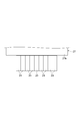
- FIG. 1 is a diagram schematically illustrating a planar configuration of an infrared detection device according to an embodiment.
- FIG. 2 is a diagram schematically illustrating a cross-sectional configuration of the infrared detection device according to the present embodiment.
- FIG. 3 is a diagram schematically showing a planar configuration of the signal processing board.
- FIG. 4 is a diagram schematically showing the positional relationship between the signal processing circuit and the heat conductive layer.
- FIG. 5 is a diagram schematically showing a positional relationship between the signal processing circuit and the heat conductive layer.
- FIG. 6 is a diagram schematically illustrating a cross-sectional configuration of an infrared detection device according to a modification of the present embodiment.
- FIG. 1 is a diagram schematically illustrating a planar configuration of an infrared detection device according to the present embodiment.
- FIG. 2 is a diagram schematically illustrating a cross-sectional configuration of the infrared detection device according to the present embodiment.
- FIG. 3 is a diagram schematically showing a planar configuration of the signal processing board.
- the infrared detection device IF includes an infrared detection element 1, a signal processing board 10 on which the infrared detection element 1 is mounted, and a support wiring board 30 on which the signal processing board 10 is mounted. It is equipped with.
- the infrared detection element 1 has a semiconductor substrate 3 having main surfaces 3a and 3b facing each other.
- the semiconductor substrate 3 is, for example, an n-type semiconductor substrate.
- the semiconductor substrate 3 has a rectangular shape (for example, a square shape) when viewed from a direction orthogonal to the semiconductor substrate 3 (main surfaces 3a and 3b), that is, in plan view.
- the infrared detection element 1 has a plurality of semiconductor regions 5 formed on the main surface 3 b side of the semiconductor substrate 3.
- the plurality of semiconductor regions 5 are arranged two-dimensionally.
- Each semiconductor region 5 is, for example, a p-type semiconductor region.
- the conductivity type of the semiconductor region 5 is different from the conductivity type of the semiconductor substrate 3.
- Each semiconductor region 5 has a rectangular shape (for example, a square shape) in plan view.
- Each semiconductor region 5 may have a circular shape or an elliptical shape depending on the application.
- a photodiode is formed by the semiconductor substrate 3 and each semiconductor region 5.
- a photodiode formed by the semiconductor region 5 and the semiconductor substrate 3 constitutes a pixel. Therefore, in the infrared detection element 1, a plurality of pixels are arranged two-dimensionally.
- a light receiving element having sensitivity in a wavelength region in the infrared region can be used.
- Such a light receiving element includes a photodiode array of a compound optical semiconductor (for example, InGaAs, InGaAsP, InAs, InAsSb, or InSb).
- the infrared detection element 1 has a plurality of electrodes 7 that are two-dimensionally arranged corresponding to the plurality of semiconductor regions 5.
- the electrode 7 is in contact with the corresponding semiconductor region 5 and functions as an anode electrode.
- the electrode 7 has a rectangular shape (for example, a square shape) in plan view.
- the electrode 7 may have a circular shape or an oval shape depending on the application.
- the signal processing board 10 has main surfaces 10a and 10b facing each other.
- the signal processing substrate 10 is disposed so that the main surface 10 a faces the main surface 3 b of the semiconductor substrate 3.
- the signal processing substrate 10 is disposed so as to face the semiconductor substrate 3.
- the main surface 10 b is the back surface of the main surface 10 a that faces the main surface 3 b of the semiconductor substrate 3.
- the signal processing board 10 has a rectangular shape (for example, a square shape) in plan view.
- the signal processing board 10 has a pair of sides 11a and 11b facing each other and a pair of sides 11c and 11d facing each other.
- the four sides 11a, 11b, 11c, and 11d form the contour of the signal processing board 10.
- the signal processing substrate 10 has a plurality of laminated insulating layers 13.
- the plurality of insulating layers 13 are located on the main surface 10 a side of the signal processing substrate 10.
- Each insulating layer 13 functions as an interlayer insulating film.
- the signal processing substrate 10 has at least three insulating layers 13.
- Each insulating layer 13 is made of, for example, silicon oxide.
- the signal processing board 10 has an element arrangement area 17 and a circuit arrangement area 19 as shown in FIG.
- the element arrangement region 17 is located in the element arrangement region 17, the infrared detection element 1 is arranged. That is, the element arrangement region 17 is located immediately below the infrared detection element 1 (semiconductor substrate 3). In the present embodiment, the element arrangement region 17 is located at the center of the signal processing substrate 10 when viewed from the direction orthogonal to the semiconductor substrate 3.
- the element arrangement region 17 has a rectangular shape (for example, a square shape) in plan view. In FIG. 3, illustration of the insulating layer 13 and a wiring 24 described later is omitted for clarity of the structure.
- the element arrangement region 17 has a pair of sides 17a and 17b facing each other and a pair of sides 17c and 17d facing each other.
- the four sides 17a, 17b, 17c, and 17d form the outline of the element arrangement region 17.
- the pair of sides 17 a and 17 b of the element arrangement region 17 is parallel to the pair of sides 11 a and 11 b of the signal processing substrate 10.
- the pair of sides 17 c and 17 d of the element arrangement region 17 is parallel to the pair of sides 11 c and 11 d of the signal processing substrate 10.
- a plurality of electrodes 21 are arranged in the element arrangement region 17.
- the plurality of electrodes 21 are two-dimensionally arranged so as to correspond to the arrangement of the plurality of electrodes 7 (pixels).
- the plurality of electrodes 21 are formed on the insulating layer 13 located on the outermost surface.
- Corresponding electrodes 7 and electrodes 21 are connected via conductive bumps 22.
- the electrode 21 is electrically connected to the corresponding pixel.
- the electrode 21 has a rectangular shape (for example, a square shape) in plan view.
- the electrode 21 may have a circular shape or an elliptical shape depending on the application.
- the circuit arrangement area 19 is located outside the element arrangement area 17 so as to surround the element arrangement area 17 when viewed from a direction orthogonal to the signal processing board 10 (main surfaces 10a, 10b), that is, in plan view.
- the circuit arrangement region 19 is located outside the infrared detection element 1 (semiconductor substrate 3) when viewed from a direction orthogonal to the signal processing substrate 10.
- the signal processing board 10 has a plurality of signal processing circuits 23. Each signal processing circuit 23 processes a signal output from a corresponding pixel. In the present embodiment, the signal processing board 10 has “36” signal processing circuits 23 corresponding to the number of pixels.
- the signal processing circuit 23 includes, for example, a charge amplifier circuit, a source follower circuit, or an auto zero circuit. Since these circuits have configurations well known to those skilled in the art, a detailed description thereof will be omitted.
- the signal processing circuit 23 is mounted on the signal processing board 10 as an ASIC (Application Specific Integrated Circuit).
- the signal processing substrate 10 includes a substrate portion 12 on which a signal processing circuit 23 is mounted, and a plurality of insulating layers 13 are disposed on the substrate portion 12.
- the signal processing circuit 23 is electrically connected to the corresponding electrode 21 through the wiring 24 formed between the insulating layers 13. Therefore, signals output from the pixels of the infrared detection element 1 are output to the signal processing circuit 23 through the corresponding electrodes 7, conductive bumps 22, electrodes 21, and wirings 24.
- the plurality of signal processing circuits 23 are arranged in the circuit arrangement area 19 so as to surround the element arrangement area 17.
- the plurality of signal processing circuits 23 are arranged in the circuit arrangement region 19 along the four sides 11 a, 11 b, 11 c, 11 d of the signal processing board 10.
- a plurality of signal processing circuits 23 (in this embodiment, “9” signal processing circuit 23) electrically connected to the plurality of electrodes 21 arranged in the partial region 18 a are opposed to one side of the partial region 18 a.
- the signal processing board 10 is arranged along the side 11a.
- These signal processing circuits 23 are located between the partial region 18a and the side 11a when viewed from a direction orthogonal to the signal processing substrate 10.
- the signal processing circuits 23 of “9” are arranged in a line along the side 11a.
- a plurality of signal processing circuits 23 (in this embodiment, “9” signal processing circuit 23) electrically connected to the plurality of electrodes 21 arranged in the partial region 18 b are opposed to one side of the partial region 18 b.
- the signal processing board 10 is arranged along the side 11b.
- These signal processing circuits 23 are located between the partial region 18b and the side 11b when viewed from a direction orthogonal to the signal processing substrate 10.
- the signal processing circuits 23 of “9” are arranged in a line along the side 11b.
- a plurality of signal processing circuits 23 (in this embodiment, “9” signal processing circuit 23) electrically connected to the plurality of electrodes 21 arranged in the partial region 18 c are opposed to one side of the partial region 18 c.
- the signal processing board 10 is arranged along the side 11c.
- These signal processing circuits 23 are located between the partial region 18c and the side 11c when viewed from a direction orthogonal to the signal processing substrate 10.
- “9” signal processing circuits 23 are arranged in a line along the side 11c.
- a plurality of signal processing circuits 23 (in this embodiment, “9” signal processing circuit 23) electrically connected to the plurality of electrodes 21 arranged in the partial region 18 d are opposed to one side of the partial region 18 d.
- the signal processing board 10 is arranged along the side 11d.
- These signal processing circuits 23 are located between the partial region 18d and the side 11d when viewed from a direction orthogonal to the signal processing substrate 10.
- “9” signal processing circuits 23 are arranged in a line along the side 11d.
- a plurality of electrodes 25 are arranged in the circuit arrangement region 19.
- the plurality of electrodes 25 are arranged in the circuit arrangement region 19 along the four sides 11a, 11b, 11c, and 11d of the signal processing board 10.
- the plurality of electrodes 25 are formed on the insulating layer 13 located on the outermost surface.
- each electrode 25 is connected to a wiring formed in the insulating layer 13 through a contact hole penetrating the insulating layer 13.
- the output of the signal processing circuit 23 is sent to the outside of the signal processing substrate 10 through the wiring and contact holes described above and the electrode 25.
- a heat conductive layer 27 is disposed on the signal processing substrate 10.
- the thermal conductive layer 27 has a thermal conductivity higher than that of the plurality of insulating layers 13.
- the heat conductive layer 27 is a metal layer.
- the material constituting the heat conductive layer 27 is, for example, aluminum or copper.
- the heat conductive layer 27 is disposed on at least one insulating layer 13 and positioned in the element disposition region 17. In this embodiment, it arrange
- the heat conductive layer 27 has a layer portion 27 a located in the element placement region 17 and a layer portion 27 b located in the circuit placement region 19.
- the layer portion 27a has the same rectangular shape (for example, a square shape) as the element arrangement region 17 in plan view.
- the layer portion 27b is located outside the layer portion 27a so as to surround the layer portion 27a in plan view.
- the end of the heat conductive layer 27 substantially coincides with the end of the signal processing circuit 23 when viewed from the direction orthogonal to the signal processing substrate 10.
- the insulating layer 13 and the wiring 24 are not shown for the sake of clarity, and only the heat conductive layer 27 and the signal processing circuit 23 are shown.
- the heat conductive layer 27 is formed in a solid shape.
- the heat conductive layer 27 has a rectangular shape (for example, a square shape) in plan view.
- the heat conductive layer 27 is not necessarily formed in a solid shape.
- the heat conductive layer 27 may be formed in a lattice shape.
- a plurality of openings may be formed in the heat conductive layer 27.
- the heat conductive layer 27 is connected to the ground potential through a wiring (not shown).
- the support wiring substrate 30 has a plurality of electrodes 31 and electrodes 35.
- the plurality of electrodes 31 and the electrode 35 are disposed on the surface on which the signal processing board 10 is mounted.
- Each electrode 31 is electrically connected to the corresponding electrode 25.
- the electrode 31 and the electrode 25 are electrically connected by a bonding wire W.
- the electrode 35 is in contact with the main surface 10 b side of the signal processing substrate 10.
- the plurality of signal processing circuits 23 are arranged in the circuit arrangement area 19 located outside the element arrangement area 17 so as to surround the element arrangement area 17.
- heat is generated compared to the conventional configuration in which the plurality of signal processing circuits are arranged in a region located directly below the infrared detection element.
- the distance from the source signal processing circuit 23 to the infrared detection element 1 is long.
- the infrared detection element 1 is less affected by the heat from the signal processing substrate 10 because the infrared detection element 1 is separated from the signal processing circuit 23 as compared with the conventional configuration. For this reason, in the infrared detection device IF, an increase in dark current in the infrared detection element 1 can be suppressed.
- the dark current generated in the infrared detecting element 1 has temperature dependency.
- the dark current increases as the temperature of the infrared detection element 1 increases, and the dark current decreases as the temperature of the infrared detection element 1 decreases.
- a cooling device for example, a Peltier element
- the temperature near the signal processing circuit 23 may be different from the temperature away from the signal processing circuit 23. That is, a temperature gradient may occur in the element arrangement region 17. For example, the temperature near the signal processing circuit 23 is higher than the temperature away from the signal processing circuit 23.
- the pixel arranged opposite to the position near the signal processing circuit 23 in the element arrangement region 17 and the position away from the signal processing circuit 23 in the element arrangement region 17 are opposed. Therefore, the influence of heat from the signal processing board 10 is different from the pixels arranged in the same manner. For example, a pixel arranged opposite to the signal processing circuit 23 in the element arrangement region 17 is compared with a pixel arranged opposite to a position away from the signal processing circuit 23 in the element arrangement region 17. As a result, the temperature tends to increase, and the dark current may increase. The dark current may vary between the pixels of the infrared detection element 1.
- the heat conductive layer 27 is arranged on the signal processing substrate 10 so as to be located on at least one insulating layer 13 and in the element arrangement region 17. Therefore, in the infrared detection device IF including the heat conduction layer 27, for example, heat from the signal processing circuit 23 is easily transmitted to the element arrangement region 17 as compared with an infrared detection device not including the heat conduction layer 27. A temperature gradient hardly occurs in the element arrangement region 17. For this reason, in the infrared detection element 1, it can suppress that a dark current varies between pixels.
- the temperature distribution in the region located directly below the infrared detection element 1 becomes substantially uniform with the passage of time from the start of driving of the infrared detection device IF. It is conceivable that no gradient occurs.
- the infrared detector IF including the heat conductive layer 27 is, for example, until the temperature distribution in the element arrangement region 17 becomes substantially uniform as compared with the infrared detector not including the heat conductive layer 27. The period is short. For this reason, in the infrared detection device IF, the period during which the dark current variation occurs between the pixels of the infrared detection element 1 is relatively short. Therefore, the influence of dark current variation is suppressed to the detection result of the infrared detector IF. As a result, the infrared detection device IF can perform infrared detection with higher accuracy.
- the heat conductive layer 27 is a solid metal layer.
- the heat conductive layer 27 can be formed by the same process as the wiring 24 formed between the insulating layers 13. For this reason, a configuration in which a temperature gradient hardly occurs in the element arrangement region 17 can be easily realized. Since the heat conductive layer 27 has a solid shape, the heat generated in the signal processing circuit 23 is effectively transmitted to the element arrangement region 17.
- the heat conductive layer 27 is disposed so as to be positioned between two adjacent insulating layers 13. In this case, the heat conductive layer 27 is located in the signal processing board 10 rather than the surface of the signal processing board 10 facing the infrared detection element 1 (semiconductor substrate 3).
- the heat conductive layer 27 is located in the signal processing substrate 10, for example, compared with the case where the heat conductive layer 27 is disposed on the surface of the signal processing substrate 10 facing the infrared detection element 1, Since the distance from the layer 27 to the infrared detection element 1 is long, the infrared detection element 1 is hardly affected by the heat from the heat conductive layer 27. For this reason, in the infrared detection device IF, it is possible to further suppress the increase in dark current in the infrared detection element 1 and to suppress variations in dark current among pixels.
- the signal processing board 10 has a rectangular shape in plan view.
- the plurality of signal processing circuits 23 are arranged in the circuit arrangement region 19 along the sides 11a, 11b, 11c, and 11d of the signal processing board 10. In this case, since heat is transmitted to the element arrangement region 17 from the sides 11a, 11b, 11c, and 11d, that is, from four directions, in the infrared detection device IF, a temperature gradient is hardly generated in the element arrangement region 17. .
- the element arrangement region 17 has a rectangular shape having four sides 17a, 17b, 17c, and 17d in plan view.
- a plurality of electrodes 21 are two-dimensionally arranged in the element arrangement region 17 so as to correspond to the arrangement of the plurality of pixels in the infrared detection element 1.
- the element arrangement region 17 includes four rectangular partial regions 18a, 18b, 18c, and 18d.
- the electrodes 21 arranged in the four partial regions 18a, 18b, 18c, and 18d are arranged on the sides 11a, 11b, 11c, and 11d of the signal processing substrate 10 facing one side of each partial region 18a, 18b, 18c, and 18d. It is connected to a signal processing circuit 23 arranged along the line. For this reason, a temperature gradient is hardly generated in the element arrangement region 17.
- Each signal processing circuit 23 arranged along each side 11a, 11b, 11c, 11d of the signal processing board 10 and the electrode 21 corresponding to the signal processing circuit 23 can be appropriately connected.
- the end of the heat conductive layer 27 and the end of the signal processing circuit 23 do not necessarily need to coincide when viewed from the direction orthogonal to the signal processing substrate 10.
- the end of the heat conductive layer 27 may be separated from the end of the signal processing circuit 23, or the end of the heat conductive layer 27 may be separated from the signal processing circuit 23. May overlap.
- the signal processing is performed when viewed from the direction orthogonal to the signal processing board 10.
- the heat of the signal processing circuit 23 is not easily transferred to the heat conducting layer 27 as compared with the case where it substantially coincides with the end of the circuit 23.
- the end of the heat conduction layer 27 overlaps with the signal processing circuit 23
- stray capacitance is generated between the heat conduction layer 27 and the signal processing circuit 23, and the stray capacitance affects the characteristics of the signal processing circuit 23. There is a fear.
- FIG. 5 is a diagram schematically showing a positional relationship between the signal processing circuit and the heat conductive layer.
- the configuration of the heat conductive layer 27 is different from that of the above-described embodiment.
- FIG. 5 only the heat conductive layer 27 and the signal processing circuit 23 are shown for clarity of the structure, as in FIG. 4.
- the heat conductive layer 27 includes a layer portion 27a, a layer portion 27b, and a plurality of layer portions 27c.
- the plurality of layer portions 27 c are located in the circuit arrangement region 19.
- Each layer portion 27 c is located between adjacent signal processing circuits 23 when viewed from a direction orthogonal to the signal processing substrate 10.
- the heat conductive layer 27 has a layer portion 27 c located between adjacent signal processing circuits 23 when viewed from a direction orthogonal to the signal processing substrate 10, heat from the signal processing circuit 23 is obtained. Is transmitted to the layer portion 27c, and further from the layer portion 27c to the layer portion 27a through the layer portion 27b. For this reason, since heat from the signal processing circuit 23 is easily transferred to the heat conducting layer 27, a temperature gradient is hardly generated in the element arrangement region 17.
- the layer portions 27 a and 27 b and the respective layer portions 27 c may be located between the same insulating layers 13, or may be located on different insulating layers 13.
- FIG. 6 is a diagram schematically illustrating a cross-sectional configuration of the infrared detection device according to the present modification.
- the infrared detection device IF shown in FIG. 6 includes an infrared detection element 1, a signal processing board 10, and a support wiring board 30.
- a plurality of heat conducting members 29 are arranged on the signal processing board 10.
- Each heat conducting member 29 has one end 29 a connected to the heat conducting layer 27 and the other end 29 b located on the main surface 10 b side of the signal processing board 10. Similar to the heat conductive layer 27, the heat conductive member 29 has a heat conductivity higher than the heat conductivity of the plurality of insulating layers 13.
- the heat conducting member 29 is a metal member.
- the material constituting the heat conducting member 29 is, for example, aluminum or copper.
- the heat conducting member 29 is formed so as to penetrate the substrate portion 12 in the thickness direction of the signal processing substrate 10. One end 29 a and the other end 29 b of the heat conducting member 29 are exposed from the substrate portion 12. The other end 29 b of the heat conducting member 29 is connected to the electrode 35. By connecting the electrode 35 to the ground potential, the heat conduction layer 27 is given a ground potential through the heat conduction member 29.
- Part of the heat of the heat conductive layer 27 is transmitted to the main surface 10b side of the signal processing substrate 10 through the heat conductive member 29. Since the heat transmitted to the main surface 10b side is dissipated from the signal processing substrate 10, the temperature of the heat conductive layer 27 is lowered. For this reason, in this modification, it can suppress that the dark current changes between pixels, suppressing the increase in the dark current in the infrared detection element 1 further.
- Each shape of the semiconductor substrate 3, the semiconductor region 5, the signal processing substrate 10, the element arrangement region 17, the heat conductive layer 27, and the electrodes 7 and 21 is not limited to the above-described rectangular shape. These shapes may be circular, for example.
- the numbers of the semiconductor region 5, the electrodes 7, 21 and the signal processing circuit 23 are not limited to the numbers described above.
- the present invention can be used for an infrared detector.
- SYMBOLS 1 ... Infrared detection element, 3 ... Semiconductor substrate, 5 ... Semiconductor area
Landscapes
- Physics & Mathematics (AREA)
- General Physics & Mathematics (AREA)
- Engineering & Computer Science (AREA)
- Power Engineering (AREA)
- Spectroscopy & Molecular Physics (AREA)
- Electromagnetism (AREA)
- Condensed Matter Physics & Semiconductors (AREA)
- Computer Hardware Design (AREA)
- Microelectronics & Electronic Packaging (AREA)
- Signal Processing (AREA)
- Multimedia (AREA)
- Photometry And Measurement Of Optical Pulse Characteristics (AREA)
- Solid State Image Pick-Up Elements (AREA)
- Transforming Light Signals Into Electric Signals (AREA)
- Light Receiving Elements (AREA)
- Studio Devices (AREA)
Abstract
Priority Applications (5)
| Application Number | Priority Date | Filing Date | Title |
|---|---|---|---|
| CN201580076369.3A CN107250738B (zh) | 2015-02-18 | 2015-11-19 | 红外线检测装置 |
| KR1020177024798A KR20170118107A (ko) | 2015-02-18 | 2015-11-19 | 적외선 검출 장치 |
| EP15882717.0A EP3260827B1 (fr) | 2015-02-18 | 2015-11-19 | Dispositif de détection infrarouge |
| US15/550,127 US10480995B2 (en) | 2015-02-18 | 2015-11-19 | Infrared detection device |
| US16/594,706 US20200041336A1 (en) | 2015-02-18 | 2019-10-07 | Infrared detection device |
Applications Claiming Priority (2)
| Application Number | Priority Date | Filing Date | Title |
|---|---|---|---|
| JP2015029928A JP2016151523A (ja) | 2015-02-18 | 2015-02-18 | 赤外線検出装置 |
| JP2015-029928 | 2015-02-18 |
Related Child Applications (2)
| Application Number | Title | Priority Date | Filing Date |
|---|---|---|---|
| US15/550,127 A-371-Of-International US10480995B2 (en) | 2015-02-18 | 2015-11-19 | Infrared detection device |
| US16/594,706 Continuation US20200041336A1 (en) | 2015-02-18 | 2019-10-07 | Infrared detection device |
Publications (1)
| Publication Number | Publication Date |
|---|---|
| WO2016132616A1 true WO2016132616A1 (fr) | 2016-08-25 |
Family
ID=56692119
Family Applications (1)
| Application Number | Title | Priority Date | Filing Date |
|---|---|---|---|
| PCT/JP2015/082579 WO2016132616A1 (fr) | 2015-02-18 | 2015-11-19 | Dispositif de détection infrarouge |
Country Status (6)
| Country | Link |
|---|---|
| US (2) | US10480995B2 (fr) |
| EP (1) | EP3260827B1 (fr) |
| JP (1) | JP2016151523A (fr) |
| KR (1) | KR20170118107A (fr) |
| CN (2) | CN110793627A (fr) |
| WO (1) | WO2016132616A1 (fr) |
Families Citing this family (2)
| Publication number | Priority date | Publication date | Assignee | Title |
|---|---|---|---|---|
| KR20180064628A (ko) * | 2016-12-05 | 2018-06-15 | 삼성디스플레이 주식회사 | 액정표시장치 |
| JP6820789B2 (ja) * | 2017-04-07 | 2021-01-27 | セイコーNpc株式会社 | 赤外線センサ装置 |
Citations (7)
| Publication number | Priority date | Publication date | Assignee | Title |
|---|---|---|---|---|
| JPH0734334U (ja) * | 1993-12-01 | 1995-06-23 | 株式会社村田製作所 | 赤外線アレイセンサ |
| JP2003152170A (ja) * | 2001-11-15 | 2003-05-23 | Toshiba Corp | 赤外線センサ |
| JP2006128196A (ja) * | 2004-10-26 | 2006-05-18 | Sony Corp | 半導体イメージセンサー・モジュール及びその製造方法 |
| JP2008232863A (ja) * | 2007-03-21 | 2008-10-02 | Seiko Npc Corp | 赤外線センサ装置 |
| JP2008541102A (ja) * | 2005-05-17 | 2008-11-20 | ハイマン・ゼンゾル・ゲゼルシャフト・ミト・ベシュレンクテル・ハフツング | サーモパイル赤外線センサアレイ |
| JP2012216585A (ja) * | 2011-03-31 | 2012-11-08 | Hamamatsu Photonics Kk | フォトダイオードアレイモジュール及びその製造方法 |
| JP2013126000A (ja) * | 2011-12-13 | 2013-06-24 | Fujitsu Ltd | 赤外線撮像装置 |
Family Cites Families (10)
| Publication number | Priority date | Publication date | Assignee | Title |
|---|---|---|---|---|
| FR2460079A1 (fr) * | 1979-06-27 | 1981-01-16 | Thomson Csf | Mosaique de detecteurs de rayonnement lue par un dispositif semi-conducteur, et systeme de prise de vues comportant une telle mosaique |
| JP3921320B2 (ja) | 2000-01-31 | 2007-05-30 | 日本電気株式会社 | 熱型赤外線検出器およびその製造方法 |
| KR101260634B1 (ko) * | 2004-05-11 | 2013-05-03 | 하마마츠 포토닉스 가부시키가이샤 | 방사선 촬상 장치 |
| JP5172267B2 (ja) * | 2007-10-09 | 2013-03-27 | 富士フイルム株式会社 | 撮像装置 |
| JP5255873B2 (ja) * | 2008-03-17 | 2013-08-07 | 浜松ホトニクス株式会社 | 光検出器 |
| JP5489705B2 (ja) * | 2009-12-26 | 2014-05-14 | キヤノン株式会社 | 固体撮像装置および撮像システム |
| JP2011142558A (ja) | 2010-01-08 | 2011-07-21 | Fujitsu Ltd | イメージセンサおよび撮像システム |
| JP5682327B2 (ja) * | 2011-01-25 | 2015-03-11 | ソニー株式会社 | 固体撮像素子、固体撮像素子の製造方法、及び電子機器 |
| KR101808375B1 (ko) * | 2011-06-10 | 2017-12-12 | 플리어 시스템즈, 인크. | 저전력 소형 폼 팩터 적외선 이미징 |
| CN205157061U (zh) * | 2012-12-26 | 2016-04-13 | 菲力尔系统公司 | 红外传感器模块和红外成像设备 |
-
2015
- 2015-02-18 JP JP2015029928A patent/JP2016151523A/ja active Pending
- 2015-11-19 KR KR1020177024798A patent/KR20170118107A/ko not_active Application Discontinuation
- 2015-11-19 EP EP15882717.0A patent/EP3260827B1/fr not_active Not-in-force
- 2015-11-19 CN CN201911202243.2A patent/CN110793627A/zh active Pending
- 2015-11-19 US US15/550,127 patent/US10480995B2/en active Active
- 2015-11-19 WO PCT/JP2015/082579 patent/WO2016132616A1/fr active Application Filing
- 2015-11-19 CN CN201580076369.3A patent/CN107250738B/zh not_active Expired - Fee Related
-
2019
- 2019-10-07 US US16/594,706 patent/US20200041336A1/en not_active Abandoned
Patent Citations (7)
| Publication number | Priority date | Publication date | Assignee | Title |
|---|---|---|---|---|
| JPH0734334U (ja) * | 1993-12-01 | 1995-06-23 | 株式会社村田製作所 | 赤外線アレイセンサ |
| JP2003152170A (ja) * | 2001-11-15 | 2003-05-23 | Toshiba Corp | 赤外線センサ |
| JP2006128196A (ja) * | 2004-10-26 | 2006-05-18 | Sony Corp | 半導体イメージセンサー・モジュール及びその製造方法 |
| JP2008541102A (ja) * | 2005-05-17 | 2008-11-20 | ハイマン・ゼンゾル・ゲゼルシャフト・ミト・ベシュレンクテル・ハフツング | サーモパイル赤外線センサアレイ |
| JP2008232863A (ja) * | 2007-03-21 | 2008-10-02 | Seiko Npc Corp | 赤外線センサ装置 |
| JP2012216585A (ja) * | 2011-03-31 | 2012-11-08 | Hamamatsu Photonics Kk | フォトダイオードアレイモジュール及びその製造方法 |
| JP2013126000A (ja) * | 2011-12-13 | 2013-06-24 | Fujitsu Ltd | 赤外線撮像装置 |
Non-Patent Citations (1)
| Title |
|---|
| See also references of EP3260827A4 * |
Also Published As
| Publication number | Publication date |
|---|---|
| EP3260827A1 (fr) | 2017-12-27 |
| CN107250738B (zh) | 2019-12-31 |
| US20180238733A1 (en) | 2018-08-23 |
| JP2016151523A (ja) | 2016-08-22 |
| EP3260827B1 (fr) | 2019-07-10 |
| CN110793627A (zh) | 2020-02-14 |
| EP3260827A4 (fr) | 2018-10-24 |
| US10480995B2 (en) | 2019-11-19 |
| CN107250738A (zh) | 2017-10-13 |
| KR20170118107A (ko) | 2017-10-24 |
| US20200041336A1 (en) | 2020-02-06 |
Similar Documents
| Publication | Publication Date | Title |
|---|---|---|
| CN108695349B (zh) | 具有层压层的半导体装置和设备 | |
| JP5842118B2 (ja) | 赤外線センサ | |
| US11374043B2 (en) | Photodetection device with matrix array of avalanche diodes | |
| WO2010113938A1 (fr) | Capteur matriciel infrarouge | |
| US9129880B2 (en) | Imaging device | |
| TWI704686B (zh) | 光檢測裝置 | |
| JP2011159984A (ja) | 半導体光検出素子及び放射線検出装置 | |
| US20130092822A1 (en) | Solid-state imaging apparatus | |
| JP6839713B2 (ja) | 光検出装置 | |
| CN113167638B (zh) | 光检测装置 | |
| JP2010237118A (ja) | 赤外線アレイセンサ | |
| US11658192B2 (en) | Image sensor and image-capturing device | |
| US20200041336A1 (en) | Infrared detection device | |
| JP2014165417A (ja) | 半導体装置 | |
| JP5085122B2 (ja) | 半導体光検出素子及び放射線検出装置 | |
| WO2019146725A1 (fr) | Dispositif photodétecteur | |
| JP2012173156A (ja) | 赤外線センサモジュール | |
| US10811459B2 (en) | Backside incidence type solid-state image pickup device | |
| US7045761B2 (en) | Self-pixelating focal plane array with electronic output | |
| TW202316087A (zh) | 雪崩光電二極體陣列 | |
| WO2022138050A1 (fr) | Capteur de détection de rayonnement et détecteur d'image de rayonnement | |
| JP2009064982A (ja) | 固体撮像素子 | |
| WO2013105270A1 (fr) | Unité de dispositif de réception de lumière, dispositif d'imagerie par polarisation, et appareil |
Legal Events
| Date | Code | Title | Description |
|---|---|---|---|
| 121 | Ep: the epo has been informed by wipo that ep was designated in this application |
Ref document number: 15882717 Country of ref document: EP Kind code of ref document: A1 |
|
| REEP | Request for entry into the european phase |
Ref document number: 2015882717 Country of ref document: EP |
|
| WWE | Wipo information: entry into national phase |
Ref document number: 15550127 Country of ref document: US |
|
| NENP | Non-entry into the national phase |
Ref country code: DE |
|
| ENP | Entry into the national phase |
Ref document number: 20177024798 Country of ref document: KR Kind code of ref document: A |