US9129880B2 - Imaging device - Google Patents
Imaging device Download PDFInfo
- Publication number
- US9129880B2 US9129880B2 US14/134,886 US201314134886A US9129880B2 US 9129880 B2 US9129880 B2 US 9129880B2 US 201314134886 A US201314134886 A US 201314134886A US 9129880 B2 US9129880 B2 US 9129880B2
- Authority
- US
- United States
- Prior art keywords
- pixel
- pixels
- layers
- layer
- imaging device
- Prior art date
- Legal status (The legal status is an assumption and is not a legal conclusion. Google has not performed a legal analysis and makes no representation as to the accuracy of the status listed.)
- Active
Links
- 238000003384 imaging method Methods 0.000 title claims abstract description 41
- 238000010521 absorption reaction Methods 0.000 claims abstract description 99
- 229910052738 indium Inorganic materials 0.000 claims description 4
- APFVFJFRJDLVQX-UHFFFAOYSA-N indium atom Chemical compound [In] APFVFJFRJDLVQX-UHFFFAOYSA-N 0.000 claims description 4
- 238000003475 lamination Methods 0.000 claims description 4
- 239000000758 substrate Substances 0.000 description 40
- 239000010408 film Substances 0.000 description 25
- 229910052751 metal Inorganic materials 0.000 description 17
- 239000002184 metal Substances 0.000 description 17
- JBRZTFJDHDCESZ-UHFFFAOYSA-N AsGa Chemical compound [As]#[Ga] JBRZTFJDHDCESZ-UHFFFAOYSA-N 0.000 description 16
- 229910001218 Gallium arsenide Inorganic materials 0.000 description 15
- 230000015572 biosynthetic process Effects 0.000 description 11
- 230000000052 comparative effect Effects 0.000 description 11
- 238000004519 manufacturing process Methods 0.000 description 11
- 238000010586 diagram Methods 0.000 description 8
- 239000008186 active pharmaceutical agent Substances 0.000 description 7
- 239000000872 buffer Substances 0.000 description 6
- 238000001514 detection method Methods 0.000 description 6
- 238000003331 infrared imaging Methods 0.000 description 6
- 238000000926 separation method Methods 0.000 description 6
- 238000000034 method Methods 0.000 description 5
- 230000035945 sensitivity Effects 0.000 description 5
- VYPSYNLAJGMNEJ-UHFFFAOYSA-N Silicium dioxide Chemical compound O=[Si]=O VYPSYNLAJGMNEJ-UHFFFAOYSA-N 0.000 description 4
- 238000001312 dry etching Methods 0.000 description 4
- 239000000463 material Substances 0.000 description 4
- 238000001020 plasma etching Methods 0.000 description 4
- 239000010409 thin film Substances 0.000 description 4
- 230000008859 change Effects 0.000 description 3
- 230000007423 decrease Effects 0.000 description 3
- 229910000530 Gallium indium arsenide Inorganic materials 0.000 description 2
- XUIMIQQOPSSXEZ-UHFFFAOYSA-N Silicon Chemical compound [Si] XUIMIQQOPSSXEZ-UHFFFAOYSA-N 0.000 description 2
- 230000008901 benefit Effects 0.000 description 2
- 238000002161 passivation Methods 0.000 description 2
- 238000005268 plasma chemical vapour deposition Methods 0.000 description 2
- 239000004065 semiconductor Substances 0.000 description 2
- 229910052710 silicon Inorganic materials 0.000 description 2
- 239000010703 silicon Substances 0.000 description 2
- 235000012239 silicon dioxide Nutrition 0.000 description 2
- 239000000377 silicon dioxide Substances 0.000 description 2
- KXNLCSXBJCPWGL-UHFFFAOYSA-N [Ga].[As].[In] Chemical compound [Ga].[As].[In] KXNLCSXBJCPWGL-UHFFFAOYSA-N 0.000 description 1
- 230000004075 alteration Effects 0.000 description 1
- 239000013590 bulk material Substances 0.000 description 1
- 238000005229 chemical vapour deposition Methods 0.000 description 1
- 230000005284 excitation Effects 0.000 description 1
- 230000004907 flux Effects 0.000 description 1
- 230000006870 function Effects 0.000 description 1
- 238000009413 insulation Methods 0.000 description 1
- 238000002955 isolation Methods 0.000 description 1
- 238000005304 joining Methods 0.000 description 1
- 230000031700 light absorption Effects 0.000 description 1
- 239000011159 matrix material Substances 0.000 description 1
- 238000003801 milling Methods 0.000 description 1
- 230000004297 night vision Effects 0.000 description 1
- 230000003287 optical effect Effects 0.000 description 1
- 230000008520 organization Effects 0.000 description 1
- 238000003825 pressing Methods 0.000 description 1
- 230000008569 process Effects 0.000 description 1
- 239000002096 quantum dot Substances 0.000 description 1
- 229910000679 solder Inorganic materials 0.000 description 1
- 238000006467 substitution reaction Methods 0.000 description 1
- VLCQZHSMCYCDJL-UHFFFAOYSA-N tribenuron methyl Chemical compound COC(=O)C1=CC=CC=C1S(=O)(=O)NC(=O)N(C)C1=NC(C)=NC(OC)=N1 VLCQZHSMCYCDJL-UHFFFAOYSA-N 0.000 description 1
Images


Classifications
-
- H—ELECTRICITY
- H01—ELECTRIC ELEMENTS
- H01L—SEMICONDUCTOR DEVICES NOT COVERED BY CLASS H10
- H01L27/00—Devices consisting of a plurality of semiconductor or other solid-state components formed in or on a common substrate
- H01L27/14—Devices consisting of a plurality of semiconductor or other solid-state components formed in or on a common substrate including semiconductor components sensitive to infrared radiation, light, electromagnetic radiation of shorter wavelength or corpuscular radiation and specially adapted either for the conversion of the energy of such radiation into electrical energy or for the control of electrical energy by such radiation
- H01L27/144—Devices controlled by radiation
- H01L27/146—Imager structures
- H01L27/14643—Photodiode arrays; MOS imagers
- H01L27/14649—Infrared imagers
- H01L27/14652—Multispectral infrared imagers, having a stacked pixel-element structure, e.g. npn, npnpn or MQW structures
Definitions
- a certain aspect of the embodiments is related to an imaging device.
- An infrared imaging device known as an imaging device measures the surface temperature of an object by non-contact in a remote position by incident infrared rays, and is used for detection of the form of the object.
- the infrared imaging device is used for wide uses, such as a measuring device and a control device in a manufacturing line, a diagnostic device in medical treatment, and a night vision camera and a sensor device, for example.
- An infrared imaging device provides an image of the incident infrared rays by use of reflecting mirrors and lenses, and acquires an image by changing the infrared rays into an electric pixel signal.
- An infrared sensor array includes a plurality of sensor elements arranged in the shape of a two-dimensional matrix, and a readout circuit that reads out pixel data from the sensor elements, for example.
- the sensor elements and the readout circuit are formed on separate substrates, respectively, and are connected to each other via a conductive bump.
- a substrate of the sensor elements is formed of gallium arsenide (GaAs) or the like, for example.
- a substrate of the readout circuit is formed of silicon (Si) or the like.
- Patent Document see Japanese Laid-open Patent Publication No. 2009-164302
- non-Patent Document see “Demonstration of Megapixel Dual-Band QWIP Focal Plane Array”, IEEE JOURNAL OF QUANTUM ELECTRONICS, (United States of America), 2010 February, VOL. 46, NO. 2, p. 285)
- QWIP Quadratum Well Infrared Photodetector
- MQW Multi Quantum Well
- an imaging device including: a plurality of first absorption layers that absorb an infrared ray with a given wavelength range, and generate pixel signals of a plurality of pixels, respectively; at least one second absorption layer that absorbs an infrared ray with a wavelength range which is different from the given wavelength range of the first absorption layers, and generates a pixel signal common to the pixels; a plurality of first electrodes that take out the pixel signals from the first absorption layers, respectively; and a second electrode that takes out the pixel signal from the at least one second absorption layer.
- FIG. 1 is a side view of two aligned substrates
- FIG. 2 is a side view of two substrates in which flip chip bonding is performed
- FIG. 3 is a plane view illustrating arrangement of bumps of an imaging device according to an embodiment
- FIG. 4 is a cross-section view illustrating a cross-section surface taken along a IV-IV line of FIG. 3 ;
- FIG. 5 is a plane view of upper absorption layers and upper contact layers illustrated in FIG. 3 ;
- FIG. 6 is a plane view of a lower absorption layer, a middle contact layer, and a lower contact layer illustrated in FIG. 3 ;
- FIG. 7 is a plane view illustrating another example of the lower absorption layer, the middle contact layer, and the lower contact layer;
- FIG. 8 is a diagram illustrating pixel signals taken out from the upper absorption layers and the lower absorption layer
- FIG. 9 is a diagram illustrating parameters about an interval between the bumps.
- FIG. 10 is a graph illustrating the change of each distance between the bumps to deviation of the bumps
- FIG. 11 is a plane view illustrating arrangement of bumps of an imaging device according to a comparative example
- FIG. 12 is a cross-section view illustrating a manufacturing process of the imaging device
- FIG. 13 is a cross-section view illustrating a manufacturing process of the imaging device
- FIG. 14 is a cross-section view illustrating a manufacturing process of the imaging device
- FIG. 15 is a cross-section view illustrating a manufacturing process of the imaging device
- FIG. 16 is a cross-section view illustrating a manufacturing process of the imaging device
- FIG. 17 is a cross-section view illustrating a manufacturing process of the imaging device
- FIG. 18 is a plane view illustrating arrangement of bumps of the imaging device according to another embodiment.
- FIG. 19 is a diagram illustrating pixel signals taken out from the upper absorption layers and the lower absorption layer
- FIG. 20 is a plane view illustrating arrangement of bumps of the imaging device according to the comparative example.
- FIG. 21 is a block diagram illustrating an example of functional configuration of a signal processing circuit.
- the bump which is an electrode shifts in a direction along a board face of the substrate, and the bump of a connection target contacts another bump (i.e., a bump to be unconnected) adjacent to the bump. Since arrangement accuracy has a limit, it is inescapable that the error arises in arrangement of the substrate. Therefore, by extending an interval between bumps in each substrate, it is desirable to avoid the contact between the bumps which cause a problem.
- non-Patent Document discloses a configuration in which three bumps are provided per one pixel, and a configuration in which two bumps are provided per one pixel (see FIG. 1 of non-Patent Document).
- the configuration of the former two multi-quantum well layers and three contact layers are laminated by turns, and three bumps are connected to the three contact layers through metal wirings, respectively.
- a common electrode layer is provided instead of the bump connected to a middle contact layer for applying a bias voltage among the three contacts layer, and hence the number of the bumps is reduced.
- only one bump is reduced, compared with the configuration of the former. Therefore, the interval between the bumps can be expanded.
- Patent Document discloses a configuration in which one bump is provided per one pixel (see FIG. 2 of Patent Document).
- this configuration two multi-quantum well layers and three contact layers are laminated by turns, a bias voltage is applied to a top contact layer and a bottom contact layer from the exterior, and a voltage of each wavelength range is detected from a bump connected to a middle contact layer.
- the number of bumps is minimum, and hence the interval between the bumps can be expanded, compared with the configuration disclosed in the non-Patent Document.
- the configuration disclosed by the Patent Document since in the configuration disclosed by the Patent Document, the bump which is a sensing electrode is shared between the two multi-quantum well layers, a signal current of each multi-quantum well layer needs to be detected by turns by time division (see paragraph “0022” of the Patent Document). Therefore, the configuration disclosed by the Patent Documents has a problem that a sufficient detection period is not obtained and hence sensitivity decreases, compared with other configuration.
- FIG. 1 is a side view of two aligned substrates 90 and 91 .
- One of the two substrates 90 and 91 is a sensor substrate on which an infrared detection element is formed, for example.
- Another one of the two substrates 90 and 91 is a readout circuit substrate that reads out pixel data from the sensor substrate.
- the sensor substrate is formed of gallium arsenide, for example, and includes a plurality of infrared detection elements.
- the readout circuit substrate includes a signal processing circuit that processes pixel data of the infrared detection elements as pixel signals, and the readout circuit substrate is formed of silicon or the like.
- a plurality of bumps 900 and 910 are provided with the two substrates 90 and 91 , respectively.
- the bumps 900 and 910 on the substrates 90 and 91 are formed of flexible metal such as indium. Although the two substrates 90 and 91 are arranged in an aligned state, the two substrates 90 and 91 have an error in direction H along a plate surface by a limit of the arrangement accuracy.
- FIG. 2 is a side view of the two substrates 90 and 91 in which flip chip bonding is performed. Due to the above-mentioned error, the two substrates 90 and 91 are misaligned in the direction H. Therefore, as illustrated by a code “h”, the bumps 900 and 910 contact not only the bumps 910 and 900 of connection targets but also another bumps 910 and 900 (i.e., bumps 910 and 900 which are not connection targets) adjacent to the bumps 910 and 900 of connection targets, respectively.
- another bumps 910 and 900 i.e., bumps 910 and 900 which are not connection targets
- an imaging device has a configuration which can extend an interval between the bumps.
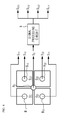
- FIG. 3 is a plane view illustrating arrangement of the bumps of the imaging device according to the embodiment. More specifically, FIG. 3 illustrates arrangement of the bumps on a plate surface of the sensor substrate.
- an infrared imaging element of the sensor substrate is a double-wavelength QWIP (Quantum Well Infrared Photodetector).
- the imaging device has a plurality of pixels arranged in an array as the infrared imaging element.
- the plurality of pixels has a shape of a square, and are divided into a plurality of sets U.
- Each of the sets U includes four adjacent pixels G 11 , G 12 , G 21 , and G 22 arranged by two lines ⁇ two rows. That is, a plurality of sets of pixels are arranged in the plane of the imaging device. In the following description, one of the plurality of sets U is explained, but the explained contents are common to each set U.
- Individual bumps (i.e., first electrodes) B 11 , B 12 , B 21 , and B 22 are provided near the centers of the pixels G 11 , G 12 , G 21 , and G 22 included in the set U (hereinafter referred to as “pixel set U”), respectively.
- the individual bumps B 11 , B 12 , B 21 , and B 22 takes out pixel signals of the four pixels G 11 , G 12 , G 21 , and G 22 , respectively.
- a common bump B C (i.e., a second electrode) which takes out a common pixel signal between the four pixels G 11 , G 12 , G 21 , and G 22 is provided in the center of the pixel set U.
- the plurality of individual bumps B 11 , B 12 , B 21 , and B 22 are arranged at equal intervals around the common bump B C so as to have optimal arrangement intervals as described later.
- Each of the bumps B C , B 11 , B 12 , B 21 , and B 22 has a circular shape in a top view, and is formed of flexible metal such as indium.
- FIG. 4 is a cross-section view illustrating a cross-section surface taken along a IV-IV line of FIG. 3 .
- the imaging device includes an insulating substrate 3 , a plurality of upper contact layers 21 , a middle contact layer 20 , a lower contact layer 22 , a plurality of upper absorption layers (i.e., first absorption layers) 11 , and a lower absorption layer (i.e., a second absorption layer) 12 .
- the imaging device further includes a surface wiring 50 , a leading wiring 52 , an insulating film 4 , metal films 60 to 62 , the individual bumps B 11 , B 12 , B 21 , and B 22 , and the common bump B C .
- the insulating substrate 3 is formed of gallium arsenide which has insulation properties.
- the lower contact layer 22 , the lower absorption layer 12 , the middle contact layer 20 , the upper absorption layers 11 , and the upper contact layers 21 are laminated on the insulating substrate 3 in this order.
- the insulating substrate 3 supports the layers 11 , 12 , and 20 to 22 .
- the contact layers 20 to 22 are formed of an n-type GaAs semiconductor, and has conductivity.
- the lower absorption layer 12 is sandwiched between the lower contact layer 22 and the middle contact layer 20 .
- Each of the upper absorption layers 11 is sandwiched between the middle contact layer 20 and each of the upper contact layers 21 . Therefore, the contact layers 20 to 22 function as electrodes of the upper absorption layers 11 and the lower absorption layer 12 .
- the upper absorption layers 11 and the lower absorption layer 12 are multi-quantum well (MQW) layers, and absorb the infrared rays of mutually different wavelength ranges. At the time of incidence of the infrared ray, electrons are excited from an excitation level to a base level by light absorption in the quantum wells of the upper absorption layers 11 and the lower absorption layer 12 . Then, when a bias voltage Vb is applied to the middle contact layer 20 , the electrons are taken out from the quantum wells to the exterior, and a photoelectric current which is the pixel signal occurs.
- Each of the upper absorption layers 11 and the lower absorption layer 12 is not limited to a layer having such quantum well structure, and may be structure using a quantum dot, bulk material, or a semiconductor layer composed of a superlattice layer.
- the insulating film 4 is a passivation film, such as a silicon dioxide film, and, cover a laminated body in whole.
- the surface wiring 50 is formed along an isolation groove between pixels, extends in a lamination direction on a side surface of the laminated body, and is connected to the middle contact layer 20 via the metal film 60 .
- the bias voltage Vb is applied from the exterior via the surface wiring 50 .
- the individual bumps B 11 and B 22 are connected to the upper contact layers 21 via metal films 61 , respectively. This is the same as the individual bumps B 12 and B 21 which are not illustrated.
- FIG. 5 is a plane view of the upper absorption layers 11 and the upper contact layers 21 illustrated in FIG. 3 .
- alternate long and short dash lines indicate boundaries between the pixels G 11 , G 12 , G 21 and G 22 .
- the upper absorption layers 11 and the upper contact layers 21 are provided for each of the pixels G 11 , G 12 , G 21 and G 22 . That is to say, the upper absorption layers 11 and the upper contact layers 21 are electrically separated for each of the pixels G 11 , G 12 , G 21 and G 22 . Therefore, in applying the bias voltage Vb, the absorption layers 11 generate the pixel signals S 11 , S 12 , S 21 , and S 22 of the pixels G 11 , G 12 , G 21 , and G 22 , respectively. As illustrated by the dotted line of FIG. 4 , the pixel signals S 11 , S 12 , S 21 , and S 22 are taken out through the individual bumps B 11 , B 12 , B 21 , and B 22 , respectively.
- FIG. 6 is a plane view of a lower absorption layer 12 , a middle contact layer 20 , and a lower contact layer 22 illustrated in FIG. 4 .
- alternate long and short dash lines indicate boundaries between the pixels G 11 , G 12 , G 21 , and G 22 .
- Each of the lower absorption layer 12 , the middle contact layer 20 , and the lower contact layer 22 is common to the pixels G 11 , G 12 , G 21 and G 22 . That is to say, each of the lower absorption layer 12 , the middle contact layer 20 , and the lower contact layer 22 has the same potential in the pixels G 11 , G 12 , G 21 and G 22 . Therefore, in applying the bias voltage Vb, the lower absorption layer 12 generates a pixel signal S C common to the pixels G 11 , G 12 , G 21 , and G 22 . The pixel signal S C is taken out through the common bump B C , as illustrated by the dotted line of FIG. 3 .
- each of the surface wiring 50 and the metal film 60 may be common to the pixels G 11 , G 12 , G 21 and G 22 , or may be separated in the pixels G 11 , G 12 , G 21 and G 22 .
- FIG. 7 only the lower contact layer 22 is common, and each of the lower absorption layer 12 and the middle contact layer 20 may be provided for each of the pixels G 11 , G 12 , G 21 and G 22 .
- each of the surface wiring 50 and the metal film 60 is provided for each of the pixels G 11 , G 12 , G 21 and G 22 in order to apply the bias voltage Vb to each lower absorption layer 12 .
- the pixel signals S 11 , S 12 , S 21 , and S 22 are generated for each of the pixels G 11 , G 12 , G 21 and G 22 by the upper absorption layers 11 , and the pixel signal S C common to the pixels G 11 , G 12 , G 21 , and G 22 is generated by the lower absorption layer 12 .
- the pixel signals S 11 , S 12 , S 21 an S 22 are taken out by the individual bumps B 11 , B 12 , B 21 , and B 22 , respectively.
- the pixel signal S C is taken out by the single common bump B C .
- the common bump B C is provided for each pixel set U, the number of common bumps B C is reduced. Since in the present embodiment, the four pixels G 11 , G 12 , G 21 and G 22 are set to the single set U, the number of the common bumps B C becomes quarter, compared with a case where the common bump B C is provided for each of the pixels G 11 , G 12 , G 21 and G 22 .
- the sensitivity does not decrease.
- the resolution of an image generated from the infrared ray which the lower absorption layer 12 absorbs is lower than that of an image generated from the infrared ray which the upper absorption layers 11 absorb because of the difference in the number of pixel signals. Therefore, processing which converts the pixel signal S C of the lower absorption layer 12 into the individual pixel signals respectively corresponding to the pixels G 11 , G 12 , G 21 , and G 22 may be performed.
- FIG. 8 is a diagram illustrating pixel signals S 11 , S 12 , S 21 , S 22 and S C taken out from the upper absorption layers 11 and the lower absorption layer 12 . Since the pixel signals S u , S 12 , S 21 and S 22 taken out from the individual bumps B 11 , B 12 , B 21 , and B 22 are acquired separately for each of the pixels G 11 , G 12 , G 21 and G 22 , the pixel signals S 11 , S 12 , S 21 and S 22 are directly used for formation processing of the image.
- the pixel signal S C taken out from the common bump B C is acquired common to the pixels G 11 , G 12 , G 21 and G 22 .
- the pixel signal S C is converted into pixel signals S C11 , S C12 , S C21 and S C22 for each of the pixels G 11 , G 12 , G 21 and G 22 by a signal processing circuit 8 .
- the signal processing circuit 8 is provided on a readout circuit substrate of the imaging device, for example. Here, detailed description of the signal processing circuit 8 is described later.
- the signal processing circuit 8 converts the pixel signal S C into the individual pixel signals S C11 , S C12 , S C21 and S C22 corresponding to the pixels G 11 , G 12 , G 21 and G 22 , respectively, based on a ratio of each intensity of the pixel signals S 11 , S 12 , S 21 and S 22 . That is, the intensities of the pixel signals S C11 , S C12 , S C21 and S C22 are acquired by the following formulas (1) to (4).
- S C11 S C ⁇ S 11 /( S 11 +S 12 +S 21 +S 22 ) (1)
- S C12 S C ⁇ S 12 /( S 11 +S 12 +S 21 +S 22 ) (2)
- S C21 S C ⁇ S 21 /( S 11 +S 12 +S 21 +S 22 ) (3)
- S C22 S C ⁇ S 22 /( S 11 +S 12 +S 21 +S 22 ) (4)
- the resolution of an image generated from the infrared ray which the lower absorption layer 12 absorbs can be improved.
- the intensities of the pixel signal S C11 , S C12 , S C21 and S C22 are artificially calculated by the formulas (1) to (4) to some extent, the intensities are hard to be called highly precise values.
- the infrared ray generates a blur (what is called “a diffraction blur) by a diffraction phenomenon due to diffraction limit when the infrared ray forms an image on the surface of the infrared detection element.
- the light flux generated by the diffraction blur spreads in the form of a circle (what is called “a blur's circle”).
- the diameter D diff of the circle is acquires by the following formula (5).
- D diff 2.44 ⁇ F (5)
- ⁇ is a wavelength of the light (i.e., the infrared ray)
- F is an F number of an optical system. If it is assumed that the F number is 2, and the wavelength ranges of the infrared rays which the upper absorption layers 11 and the lower absorption layer 12 absorb are 5 ⁇ m (middle wavelength range) and 10 ⁇ m (long wavelength range), respectively, the diameters D diff of the respective wavelength ranges are calculated as 24.4 ⁇ m and 48.8 ⁇ m.
- a pixel size i.e., a length of one side of the pixel
- the diameter D diff of the long wavelength range exceeds the pixel size greatly, and the blur occurs in the image.
- the wavelength range of the infrared ray which the lower absorption layer 12 absorbs is set to a long wavelength side, compared with the wavelength range of the infrared ray which the upper absorption layers 11 absorb. Therefore, the intensities of the pixel signals S C11 , S C12 , S C21 and S C22 are calculated by the formulas (1) to (4) without causing a problem of accuracy.
- the pixel signal S C taken out from the common bump B C may be directly used for the image formation processing.
- the image formation processing is performed under the conditions that the pixel of the infrared ray with the wavelength range absorbed by the lower absorption layer 12 is 4 times the pixel of the infrared ray with the wavelength range absorbed by the upper absorption layers 11 . That is, the image formation processing is performed in consideration of a difference between the resolutions of the infrared rays with the respective wavelength ranges.
- FIG. 9 is a diagram illustrating parameters about an interval between the bumps.
- a parameter “a” indicates a length of one side of each of the square-shaped pixels G 11 , G 12 , G 21 and G 22 .
- a parameter “b” indicates a distance between the centers of the common bump B C and the individual bumps B 11 , B 12 , B 21 and B 22 arranged at equal intervals around the common bump B C .
- the individual bumps B 11 , B 12 , B 21 and B 22 are arranged so as to become apexes of the square centering on the common bump B C .
- a parameter “c” indicates a distance between the centers of the individual bumps B 11 , B 12 , B 21 and B 22 between the pixel sets U adjacent to each other in an oblique direction (a direction of a diagonal line between the pixels).
- a parameter “d” indicates a distance between the centers of the individual bumps B 11 , B 12 , B 21 and B 22 between the pixel sets U adjacent to each other in a perpendicular direction or a horizontal direction.
- a parameter “x” indicates deviation between each of the center positions of the individual bumps B 11 , B 12 , B 21 and B 22 , and the center of the pixel (i.e., an intersection of a diagonal line) in the oblique direction.
- FIG. 10 is a graph illustrating the change of each distance between the bumps to the deviation of the bumps.
- the horizontal axis of the graph indicates x/a
- the vertical axis of the graph indicates b/a, c/a and d/a.
- Each of changes of b/a, c/a and d/a to x/a is calculated based on FIG. 9 .
- the distances “b”, “c”, “d” and “x” are 16.6 ⁇ m, 23.5 ⁇ m, 16.6 ⁇ m and 2.4 ⁇ m, respectively.
- FIG. 11 is a plane view illustrating arrangement of bumps of an imaging device according to a comparative example.
- This comparative example is an example of the configuration in which two bumps B X1 and B X2 are provided on one pixel G X , as described in the above-mentioned non-Patent Document.
- the pixel G X is in the form of a square, as viewed from above.
- the bumps B X1 and B X2 are arranged so that distances from a center of the square are equal mutually on the diagonal line of the square.
- a minimum value of the interval between the adjacent bumps B X1 and B X2 is calculated from FIG. 11 , and becomes 70% of the pixel size (i.e., a length of one side of the square).
- the minimum value of the interval between the bumps according the present embodiment is 83% of the pixel size “a”, as described above, and is only 13% larger than the minimum value of the comparative example.
- the permissible amount of the deviation in the present embodiment increases only 40% to that of the comparative example. Accordingly, in the flip chip bonding, the contact between the bumps which are not the connection targets can be restrained effectively.
- FIGS. 12 to 17 are cross-section views illustrating the manufacturing process of the imaging device.
- a wafer equipped with laminated structure as illustrated in FIG. 12 is prepared.
- the laminated body is formed so that an n-type GaAs layer 2 a , a MQW layer 1 a , an n-type GaAs layer 2 b , a MQW layer 1 b , and an n-type GaAs layer 2 c are laminated on the insulating substrate 3 in this order.
- the MQW layer 1 a is sandwiched between the n-type GaAs layers 2 a and 2 b
- the MQW layer 1 b is sandwiched between the n-type GaAs layers 2 b and 2 c .
- the MQW layers 1 a and 1 b differ in the material according to the wavelength range of the infrared ray having sensitivity.
- the wavelength range of the MQW layer 1 a is the middle wavelength range and the wavelength range of the MQW layer 1 b is the long wavelength range
- the material of the MQW layer 1 a is based on InGaAs (indium gallium arsenide) and the material of the MQW layer 1 b is based on GaAs (gallium arsenide).
- a contact hole 70 and pixel separation grooves 71 are formed in the laminated body, as illustrated in FIG. 13 .
- the contact hole 70 is formed near the center of the pixel set U so that each of the layers 1 a , 1 b , 2 b and 2 c except the lowermost n-type GaAs layer 2 a is penetrated.
- Each of the pixel separation grooves 71 is formed so that a plate surface of a sensor element substrate is divided for each pixel set U.
- the depth of each of the pixel separation grooves 71 is the same as the total of thicknesses of the respective layers 1 a , 1 b and 2 a to 2 c .
- the width of each of the pixel separation grooves 71 is wider in height sections of the MQW layer 1 b and the n-type GaAs layer 2 c than in other height sections.
- the n-type GaAs layer 2 a becomes the lower contact layer 22
- the MQW layer 1 a becomes the lower absorption layer 12
- the n-type GaAs layer 2 b becomes the middle contact layer 20
- the MQW layer 1 b becomes the upper absorption layers 11
- the n-type GaAs layer 2 c becomes the upper contact layers 21 .
- the insulating film 4 is formed so as to cover the surface of the whole laminated body, as illustrated in FIG. 14 .
- the insulating film 4 is a passivation film, such as a silicon dioxide film. Holes are formed in the portions of the insulating film 4 by dry etching, such as the RIE, and the metal films 60 to 62 are formed on the holes.
- the insulating film 4 is formed by a thin-film formation means, such as a plasma CVD (Chemical Vapor Deposition) method, and the metal films 60 to 62 are formed by a thin-film formation means, such as lift-off.
- the lift-off is a method in which a pattern is formed of a resist, a metal is deposited on the pattern, then the resist is removed, and hence the pattern with a metal film is formed on only portions having no resist.
- a metallic thin film is formed by using spatter, for example, and then undesired portions are removed by a dry etching means, such as milling, so that the surface wiring 50 and the leading wiring 52 are formed.
- the leading wiring 52 is formed so as to be connected to the metal film 62 inside the contact hole 70 , extend in the lamination direction, and spread on the top surface of the laminated body.
- the leading wiring 52 is annularly formed in a top view, the leading wiring 52 is not limited to this, but may be formed in other shape.
- the surface wiring 50 is formed so as to bury each pixel separation groove 71 , and is connected to the metal film 60 in an upper part of a step part of the middle contact layer 20 . Moreover, in order to connect with an output portion of the bias voltage Vb, the surface wiring 50 is formed so as to extend to an outer circumferential portion of the sensor substrate.
- the film thickness of the insulating film 4 is made to increase using a plasma CVD method, for example, so that the surface wiring 50 and the leading wiring 52 are covered, as illustrated in FIG. 16 .
- the imaging device illustrated in FIG. 4 is manufactured.
- each of the pixels G 11 , G 12 , G 21 and G 22 has a square shape, but is not limited to this, and may have other shape.
- FIG. 18 is a plane view illustrating arrangement of bumps of the imaging device according to another embodiment.
- the pixel set U S includes six pixels G A to G F having the shape of an equilateral triangle, and has the shape of a regular hexagon as a whole.
- the common bump B S and the individual bump B AS to B FS have the shape of a circle in a top view.
- the common bump B S is provided at the center position of a pixel set U S
- the individual bump B AS to B FS are provided at the center positions of regular triangles of the pixels G A to G F , respectively. That is, the individual bump B AS to B FS are arranged at equal intervals around the common bump B S .
- the layer structure of this imaging device is the same as the layer structure illustrated in FIG. 4 .
- the manufacturing processes are also the same as the manufacturing processes illustrated in FIGS. 12 to 17 .
- FIG. 19 is a diagram illustrating pixel signals taken out from the upper absorption layers 11 and the lower absorption layer 12 .
- the six individual bump B AS to B FS are connected to the six upper absorption layers 11 , respectively, and takes out the pixel signals S AS to S FS of the pixels G A to G F from the six upper absorption layers 11 , respectively.
- the common bump BS is connected to the lower absorption layer 12 , and takes out the pixel signal S O common to the pixels G A to G F from the lower absorption layer 12 .
- pixel signals S AS to S FS taken out from the individual bump B AS to B FS are directly used for the image formation processing.
- the pixel signal S O taken out from the common bump B S is converted into pixel signals S OA to S OF for the respective pixels G A to G F by the signal processing circuit 8 , as illustrated in FIG. 19 .
- the signal processing circuit 8 converts the pixel signal S O into the individual pixel signals S OA to S OF corresponding to the respective pixels G A to G F , based on a ratio of each intensity of the pixel signals S AS to S FS of the six pixels G A to G F .
- the intensities of the pixel signals S OA to S OF are acquired from the following formulas (6) to (11).
- S OA S O ⁇ S AS /( S AS +S BS +S CS +S DS +S ES +S FS ) (6)
- S OB S O ⁇ S BS /( S AS +S BS +S CS +S DS +S ES +S FS ) (7)
- S OC S O ⁇ S CS /( S AS +S BS +S CS +S DS +S ES +S FS ) (8)
- S OD S O ⁇ S DS /( S AS +S BS +S CS +S DS +S ES +S FS ) (9)
- S OE S O ⁇ S ES /( S AS +S BS +S CS +S DS +S ES +S FS ) (10)
- S OF S O ⁇ S FS /( S AS +S BS +S CS +S DS +S ES +S FS ) (11)
- the resolution of the image generated from the infrared ray which the lower absorption layer 12 absorbs can be improved, as with the previous embodiment.
- the intensities of the pixel signals S OA to S OF are artificially calculated by the formulas (6) to (11) to some extent, the intensities are hard to be called highly precise values in the another embodiment.
- the diameters D diff of the blur's circles of the middle wavelength range and the long wavelength range are calculated as 24.4 ⁇ m and 48.8 ⁇ m from the formula (5), respectively. Therefore, an area of the blur's circle of the long wavelength range is 1869 ⁇ m 2 , and is larger than the area of the pixel set U S .
- the wavelength range of the infrared ray which the lower absorption layer 12 absorbs is set to a long wavelength side, compared with the wavelength range of the infrared ray which the upper absorption layers 11 absorb. Therefore, the intensities of the pixel signals S OA to S OF are calculated by the formulas (6) to (11) without causing a problem of accuracy.
- the pixel signal S O taken out from the common bump B O may be directly used for the image formation processing.
- the image formation processing is performed under the conditions that the pixel of the infrared ray with the wavelength range absorbed by the lower absorption layer 12 is 6 times the pixel of the infrared ray with the wavelength range absorbed by the upper absorption layers 11 . That is, the image formation processing is performed in consideration of a difference between the resolutions of the infrared rays with the respective wavelength ranges.
- the individual bumps B AS to B FS are arranged at the center positions of regular triangles of the pixels G A to G F , as understood from FIG. 18 , so that the minimum value of intervals between the bumps is maximized.
- the minimum value of intervals between the bumps is 14.4 ⁇ m. Therefore, when the diameter of each bump is 8 ⁇ m, for example, the permissible amount of the deviation in the flip chip bonding (see FIG. 2 ) becomes 6.4 ⁇ m which is a difference between 14.4 ⁇ m and 8 ⁇ m.
- FIG. 20 is a plane view illustrating arrangement of the bumps of the imaging device according to the comparative example.
- the regular triangle-shaped pixels G Z are arranged vertically and horizontally, and two bumps B Z1 and B Z2 are provided for each pixel G Z .
- Each of the bumps B Z1 and B Z2 has the shape of a circle in a top view, and is arranged on a centroidal line of the regular triangle of the pixel G Z (see each dotted line).
- a distance L 1 between the bumps B Z1 of the adjacent pixels G Z is equal to a distance L 2 between the bumps B Z1 and B Z2 in the same pixel G Z .
- the permissible amount of the deviation in the flip chip bonding becomes 1.2 ⁇ m which is a difference between 9.2 ⁇ m and 8 ⁇ m. According to the imaging device of the another embodiment, the permissible amount of the deviation can be made into 5 or more times of the comparative example.
- FIG. 21 is a block diagram illustrating an example of functional configuration of the signal processing circuit 8 .
- the embodiment illustrated in FIGS. 3 to 8 is indicated as the pixel set U.
- the signal processing circuit 8 includes a plurality of buffers 80 , a switch 81 , an amplifier 82 , and an arithmetic circuit 83 .
- Each of the buffers 80 is provided for each pixel set U, and is connected to the individual bumps B 11 , B 12 , B 21 and B 22 and the common B C in the pixel set.
- the pixel signals S 11 , S 12 , S 21 and S 22 are inputted to the buffer 80 via the individual bumps B 11 , B 12 , B 21 and B 22 , respectively, and the pixel signal S C is inputted to the buffer 80 via the common bump B C .
- the buffer 80 accumulates temporarily the respective pixel signals S C11 , S C12 , S C21 , S C22 and S C .
- the switch 81 selects a set U which is a readout object of the pixel signals S C11 , S C12 , S C21 , S C22 and S C , from the plurality of sets U.
- the selection is performed sequentially by time division, and an order of the selection is not limited.
- the pixel signals S C11 , S C12 , S C21 , S C22 and S C of the selected pixel set U are inputted from the buffer 80 to the amplifier 82 via the switch 81 .
- the amplifier 82 amplifies the pixel signals S C11 , S C12 , S C21 , S C22 and S C .
- the arithmetic circuit 83 performs processing denoted by the above-mentioned formulas (1) to (4), as stated with reference to FIG. 8 . That is, the arithmetic circuit 83 converts the pixel signal S C into the individual pixel signals S C11 , S C12 , S C21 and S C22 corresponding to the respective pixels G 11 , G 12 , G 21 and G 22 , based on a ratio of each intensity of the pixel signals S 11 , S 12 , S 21 and S 22 of the pixels.
- the arithmetic circuit 83 performs processing denoted by the above-mentioned formulas (6) to (11), as stated with reference to FIG. 19 .
- the imaging device includes the plurality of upper absorption layers 11 , the lower absorption layer 12 , the plurality of individual bumps B 11 , B 12 , B 21 and B 22 , and the common bump B C .
- the upper absorption layers 11 absorb the infrared ray with a given wavelength range, and generates the pixel signals S 11 , S 12 , S 21 and S 22 of the pixels G 11 , G 12 , G 21 and G 22 , respectively.
- the lower absorption layer 12 absorbs the infrared ray with the wavelength range which is different from the wavelength range of the absorption layers 11 , and generates the pixel signal S C common to the pixels G 11 , G 12 , G 21 and G 22 .
- the individual bumps B 11 , B 12 , B 21 and B 22 take out the pixel signals S 11 , S 12 , S 21 and S 22 from the upper absorption layers 11 , respectively.
- the common bump B C takes out the pixel signal S C from the lower absorption layer 12 .
- the pixel signals S 11 , S 12 , S 21 and S 22 are generated from the pixels G 11 , G 12 , G 21 and G 22 by the upper absorption layers 11 , respectively, and the pixel signal S C common to the pixels G 11 , G 12 , G 21 and G 22 is generated by the lower absorption layer 12 .
- the pixel signals S 11 , S 12 , S 21 and S 22 are taken out by the individual bumps B 11 , B 12 , B 21 and B 22 , respectively, and the pixel signal S C is taken out by a single common bump B C .
- the single common bump B C may be provided for the pixels G 11 , G 12 , G 21 and G 22 (i.e., the pixel set U), and hence the number of common bumps B C is reduced.
- the individual bumps B 11 , B 12 , B 21 , and B 22 which is the same number as the pixel signals S 11 , S 12 , S 21 and S 22 are provided, the respective pixel signals S 11 , S 12 , S 21 and S 22 are not detected by time division as disclosed in the above-mentioned Patent Document, and are detected at the same time. Therefore, according to the imaging device of the present embodiment, the sensitivity does not decrease, and the interval between the bumps (i.e., electrodes) can be extended effectively.
Abstract
Description
S C11 =S C ·S 11/(S 11 +S 12 +S 21 +S 22) (1)
S C12 =S C ·S 12/(S 11 +S 12 +S 21 +S 22) (2)
S C21 =S C ·S 21/(S 11 +S 12 +S 21 +S 22) (3)
S C22 =S C ·S 22/(S 11 +S 12 +S 21 +S 22) (4)
D diff=2.44λF (5)
S OA =S O ·S AS/(S AS +S BS +S CS +S DS +S ES +S FS) (6)
S OB =S O ·S BS/(S AS +S BS +S CS +S DS +S ES +S FS) (7)
S OC =S O ·S CS/(S AS +S BS +S CS +S DS +S ES +S FS) (8)
S OD =S O ·S DS/(S AS +S BS +S CS +S DS +S ES +S FS) (9)
S OE =S O ·S ES/(S AS +S BS +S CS +S DS +S ES +S FS) (10)
S OF =S O ·S FS/(S AS +S BS +S CS +S DS +S ES +S FS) (11)
Claims (6)
Applications Claiming Priority (2)
| Application Number | Priority Date | Filing Date | Title |
|---|---|---|---|
| JP2013055025A JP6123397B2 (en) | 2013-03-18 | 2013-03-18 | Imaging device |
| JP2013-055025 | 2013-03-18 |
Publications (2)
| Publication Number | Publication Date |
|---|---|
| US20140264705A1 US20140264705A1 (en) | 2014-09-18 |
| US9129880B2 true US9129880B2 (en) | 2015-09-08 |
Family
ID=51523803
Family Applications (1)
| Application Number | Title | Priority Date | Filing Date |
|---|---|---|---|
| US14/134,886 Active US9129880B2 (en) | 2013-03-18 | 2013-12-19 | Imaging device |
Country Status (2)
| Country | Link |
|---|---|
| US (1) | US9129880B2 (en) |
| JP (1) | JP6123397B2 (en) |
Cited By (1)
| Publication number | Priority date | Publication date | Assignee | Title |
|---|---|---|---|---|
| US20180053805A1 (en) * | 2016-08-22 | 2018-02-22 | Fujitsu Limited | Photodetector and imaging device |
Families Citing this family (6)
| Publication number | Priority date | Publication date | Assignee | Title |
|---|---|---|---|---|
| JP6299238B2 (en) * | 2014-01-30 | 2018-03-28 | 富士通株式会社 | Image sensor |
| JP7047639B2 (en) | 2018-07-05 | 2022-04-05 | 富士通株式会社 | Manufacturing method of infrared detector, infrared detector and infrared detector |
| JP7243071B2 (en) * | 2018-08-01 | 2023-03-22 | 富士通株式会社 | Infrared detector and infrared imaging device using the same |
| CN110024127B (en) * | 2019-03-01 | 2020-05-26 | 长江存储科技有限责任公司 | Three-dimensional memory device with architecture of increased number of bit lines |
| EP3953970A4 (en) | 2019-04-11 | 2023-02-08 | HRL Laboratories LLC | Simultaneous dual-band image sensors |
| CN112086524A (en) * | 2020-08-28 | 2020-12-15 | 北京智创芯源科技有限公司 | Infrared detection device and preparation method |
Citations (7)
| Publication number | Priority date | Publication date | Assignee | Title |
|---|---|---|---|---|
| US6521967B1 (en) * | 1999-08-04 | 2003-02-18 | California Institute Of Technology | Three color quantum well infrared photodetector focal plane array |
| US6525387B2 (en) * | 2000-07-27 | 2003-02-25 | Aeg Infrarot-Module Gmbh | Multispectral photodiode |
| US20070284532A1 (en) | 2006-06-13 | 2007-12-13 | Mitsubishi Electric Corporation | Two-wavelength image sensor picking up both visible and infrared images |
| US20090152664A1 (en) * | 2007-04-18 | 2009-06-18 | Ethan Jacob Dukenfield Klem | Materials, Systems and Methods for Optoelectronic Devices |
| JP2009164302A (en) | 2007-12-28 | 2009-07-23 | Fujitsu Ltd | Image sensor and manufacturing method thereof |
| US20120068225A1 (en) * | 2010-09-16 | 2012-03-22 | Commissariat A L'energie Atomique Et Aux Energies Alternatives | Bispectral multilayer photodiode detector and method for manufacturing such a detector |
| US20120104535A1 (en) | 2010-10-28 | 2012-05-03 | Fujitsu Limited | Photodetector |
Family Cites Families (6)
| Publication number | Priority date | Publication date | Assignee | Title |
|---|---|---|---|---|
| US5581084A (en) * | 1995-06-07 | 1996-12-03 | Santa Barbara Research Center | Simultaneous two color IR detector having common middle layer metallic contact |
| CN100505321C (en) * | 2004-05-27 | 2009-06-24 | 佛文恩股份有限公司 | Non-crystalline silicon vertical color filter sensor set and its manufacture method |
| JP4700947B2 (en) * | 2004-10-20 | 2011-06-15 | 富士フイルム株式会社 | Single layer color solid-state imaging device with photoelectric conversion film |
| JP5401928B2 (en) * | 2008-11-06 | 2014-01-29 | ソニー株式会社 | Solid-state imaging device and electronic apparatus |
| JP5708321B2 (en) * | 2011-07-07 | 2015-04-30 | 富士通株式会社 | SENSOR ELEMENT ARRAY, MANUFACTURING METHOD THEREOF, AND IMAGING DEVICE |
| US9294691B2 (en) * | 2011-09-06 | 2016-03-22 | Sony Corporation | Imaging device, imaging apparatus, manufacturing apparatus and manufacturing method |
-
2013
- 2013-03-18 JP JP2013055025A patent/JP6123397B2/en active Active
- 2013-12-19 US US14/134,886 patent/US9129880B2/en active Active
Patent Citations (9)
| Publication number | Priority date | Publication date | Assignee | Title |
|---|---|---|---|---|
| US6521967B1 (en) * | 1999-08-04 | 2003-02-18 | California Institute Of Technology | Three color quantum well infrared photodetector focal plane array |
| US6525387B2 (en) * | 2000-07-27 | 2003-02-25 | Aeg Infrarot-Module Gmbh | Multispectral photodiode |
| US20070284532A1 (en) | 2006-06-13 | 2007-12-13 | Mitsubishi Electric Corporation | Two-wavelength image sensor picking up both visible and infrared images |
| JP2007333464A (en) | 2006-06-13 | 2007-12-27 | Mitsubishi Electric Corp | Two-wavelength image sensor |
| US20090152664A1 (en) * | 2007-04-18 | 2009-06-18 | Ethan Jacob Dukenfield Klem | Materials, Systems and Methods for Optoelectronic Devices |
| JP2009164302A (en) | 2007-12-28 | 2009-07-23 | Fujitsu Ltd | Image sensor and manufacturing method thereof |
| US20120068225A1 (en) * | 2010-09-16 | 2012-03-22 | Commissariat A L'energie Atomique Et Aux Energies Alternatives | Bispectral multilayer photodiode detector and method for manufacturing such a detector |
| US20120104535A1 (en) | 2010-10-28 | 2012-05-03 | Fujitsu Limited | Photodetector |
| JP2012094723A (en) | 2010-10-28 | 2012-05-17 | Fujitsu Ltd | Photo detector |
Non-Patent Citations (1)
| Title |
|---|
| Sarath D. Gunapala et al., "Demonstration of Megapixel Dual-Band QWIP Focal Plane Array", IEEE Journal of Quantum Electronics, vol. 46, No. 2, Feb. 2010, pp. 285-293. |
Cited By (2)
| Publication number | Priority date | Publication date | Assignee | Title |
|---|---|---|---|---|
| US20180053805A1 (en) * | 2016-08-22 | 2018-02-22 | Fujitsu Limited | Photodetector and imaging device |
| US10236319B2 (en) * | 2016-08-22 | 2019-03-19 | Fujitsu Limited | Photodetector and imaging device |
Also Published As
| Publication number | Publication date |
|---|---|
| JP2014183084A (en) | 2014-09-29 |
| US20140264705A1 (en) | 2014-09-18 |
| JP6123397B2 (en) | 2017-05-10 |
Similar Documents
| Publication | Publication Date | Title |
|---|---|---|
| US9129880B2 (en) | Imaging device | |
| US9163995B2 (en) | Techniques for tiling arrays of pixel elements | |
| US20090243016A1 (en) | Semiconductor device | |
| JPH11504763A (en) | Extended quantum well infrared photodetector | |
| US20160104696A1 (en) | Techniques for tiling arrays of pixel elements and fabricating hybridized tiles | |
| EP3525239A1 (en) | Photoelectric conversion apparatus and equipment | |
| US6580089B2 (en) | Multi-quantum-well infrared sensor array in spatially-separated multi-band configuration | |
| US11070748B2 (en) | Infrared detector, infrared imaging apparatus using the same, and controlling method of infrared detector | |
| US20150163425A1 (en) | Three Dimensional System-On-Chip Image Sensor Package | |
| JP6291895B2 (en) | Infrared detector and manufacturing method thereof | |
| JP7116591B2 (en) | Imaging device and its manufacturing method | |
| JP2013026285A (en) | Infrared ray detector and infrared ray detector manufacturing method | |
| JP2016031993A (en) | Solid state image pickup device and camera | |
| US10032823B2 (en) | Solid-state imaging device and imaging apparatus | |
| JP5724309B2 (en) | Infrared image sensor and infrared imaging device | |
| JP6345370B1 (en) | Infrared sensor device | |
| WO2018131216A1 (en) | Infrared sensor substrate and infrared sensor device | |
| JP2017157755A (en) | Photodetector and manufacturing method of photodetector | |
| JP2019075562A (en) | Photodetector including helmholtz resonator | |
| US11570383B2 (en) | Imaging device | |
| WO2016132616A1 (en) | Infrared detection device | |
| JP2019159080A (en) | Solid-state imaging device | |
| JP2005101332A (en) | Semiconductor device | |
| JP2013034123A (en) | Image sensor and imaging device | |
| WO2020095596A1 (en) | Imaging device |
Legal Events
| Date | Code | Title | Description |
|---|---|---|---|
| AS | Assignment |
Owner name: FUJITSU LIMITED, JAPAN Free format text: ASSIGNMENT OF ASSIGNORS INTEREST;ASSIGNOR:OZAKI, KAZUO;REEL/FRAME:032075/0520 Effective date: 20131122 |
|
| STCF | Information on status: patent grant |
Free format text: PATENTED CASE |
|
| MAFP | Maintenance fee payment |
Free format text: PAYMENT OF MAINTENANCE FEE, 4TH YEAR, LARGE ENTITY (ORIGINAL EVENT CODE: M1551); ENTITY STATUS OF PATENT OWNER: LARGE ENTITY Year of fee payment: 4 |
|
| MAFP | Maintenance fee payment |
Free format text: PAYMENT OF MAINTENANCE FEE, 8TH YEAR, LARGE ENTITY (ORIGINAL EVENT CODE: M1552); ENTITY STATUS OF PATENT OWNER: LARGE ENTITY Year of fee payment: 8 |