WO2016129536A1 - 有機el発光装置および電子機器 - Google Patents
有機el発光装置および電子機器 Download PDFInfo
- Publication number
- WO2016129536A1 WO2016129536A1 PCT/JP2016/053593 JP2016053593W WO2016129536A1 WO 2016129536 A1 WO2016129536 A1 WO 2016129536A1 JP 2016053593 W JP2016053593 W JP 2016053593W WO 2016129536 A1 WO2016129536 A1 WO 2016129536A1
- Authority
- WO
- WIPO (PCT)
- Prior art keywords
- layer
- pixel
- light
- light emitting
- organic
- Prior art date
- Legal status (The legal status is an assumption and is not a legal conclusion. Google has not performed a legal analysis and makes no representation as to the accuracy of the status listed.)
- Ceased
Links
Images

Classifications
-
- H—ELECTRICITY
- H10—SEMICONDUCTOR DEVICES; ELECTRIC SOLID-STATE DEVICES NOT OTHERWISE PROVIDED FOR
- H10K—ORGANIC ELECTRIC SOLID-STATE DEVICES
- H10K50/00—Organic light-emitting devices
- H10K50/10—OLEDs or polymer light-emitting diodes [PLED]
- H10K50/11—OLEDs or polymer light-emitting diodes [PLED] characterised by the electroluminescent [EL] layers
- H10K50/125—OLEDs or polymer light-emitting diodes [PLED] characterised by the electroluminescent [EL] layers specially adapted for multicolour light emission, e.g. for emitting white light
- H10K50/13—OLEDs or polymer light-emitting diodes [PLED] characterised by the electroluminescent [EL] layers specially adapted for multicolour light emission, e.g. for emitting white light comprising stacked EL layers within one EL unit
-
- H—ELECTRICITY
- H10—SEMICONDUCTOR DEVICES; ELECTRIC SOLID-STATE DEVICES NOT OTHERWISE PROVIDED FOR
- H10K—ORGANIC ELECTRIC SOLID-STATE DEVICES
- H10K50/00—Organic light-emitting devices
- H10K50/10—OLEDs or polymer light-emitting diodes [PLED]
- H10K50/11—OLEDs or polymer light-emitting diodes [PLED] characterised by the electroluminescent [EL] layers
-
- H—ELECTRICITY
- H10—SEMICONDUCTOR DEVICES; ELECTRIC SOLID-STATE DEVICES NOT OTHERWISE PROVIDED FOR
- H10K—ORGANIC ELECTRIC SOLID-STATE DEVICES
- H10K50/00—Organic light-emitting devices
- H10K50/10—OLEDs or polymer light-emitting diodes [PLED]
- H10K50/11—OLEDs or polymer light-emitting diodes [PLED] characterised by the electroluminescent [EL] layers
- H10K50/125—OLEDs or polymer light-emitting diodes [PLED] characterised by the electroluminescent [EL] layers specially adapted for multicolour light emission, e.g. for emitting white light
- H10K50/13—OLEDs or polymer light-emitting diodes [PLED] characterised by the electroluminescent [EL] layers specially adapted for multicolour light emission, e.g. for emitting white light comprising stacked EL layers within one EL unit
- H10K50/131—OLEDs or polymer light-emitting diodes [PLED] characterised by the electroluminescent [EL] layers specially adapted for multicolour light emission, e.g. for emitting white light comprising stacked EL layers within one EL unit with spacer layers between the electroluminescent layers
-
- H—ELECTRICITY
- H10—SEMICONDUCTOR DEVICES; ELECTRIC SOLID-STATE DEVICES NOT OTHERWISE PROVIDED FOR
- H10K—ORGANIC ELECTRIC SOLID-STATE DEVICES
- H10K50/00—Organic light-emitting devices
- H10K50/10—OLEDs or polymer light-emitting diodes [PLED]
- H10K50/14—Carrier transporting layers
- H10K50/15—Hole transporting layers
-
- H—ELECTRICITY
- H10—SEMICONDUCTOR DEVICES; ELECTRIC SOLID-STATE DEVICES NOT OTHERWISE PROVIDED FOR
- H10K—ORGANIC ELECTRIC SOLID-STATE DEVICES
- H10K50/00—Organic light-emitting devices
- H10K50/10—OLEDs or polymer light-emitting diodes [PLED]
- H10K50/14—Carrier transporting layers
- H10K50/16—Electron transporting layers
-
- H—ELECTRICITY
- H10—SEMICONDUCTOR DEVICES; ELECTRIC SOLID-STATE DEVICES NOT OTHERWISE PROVIDED FOR
- H10K—ORGANIC ELECTRIC SOLID-STATE DEVICES
- H10K59/00—Integrated devices, or assemblies of multiple devices, comprising at least one organic light-emitting element covered by group H10K50/00
- H10K59/30—Devices specially adapted for multicolour light emission
- H10K59/35—Devices specially adapted for multicolour light emission comprising red-green-blue [RGB] subpixels
-
- C—CHEMISTRY; METALLURGY
- C09—DYES; PAINTS; POLISHES; NATURAL RESINS; ADHESIVES; COMPOSITIONS NOT OTHERWISE PROVIDED FOR; APPLICATIONS OF MATERIALS NOT OTHERWISE PROVIDED FOR
- C09K—MATERIALS FOR MISCELLANEOUS APPLICATIONS, NOT PROVIDED FOR ELSEWHERE
- C09K11/00—Luminescent materials, e.g. electroluminescent or chemiluminescent
- C09K11/06—Luminescent materials, e.g. electroluminescent or chemiluminescent containing organic luminescent materials
-
- H—ELECTRICITY
- H10—SEMICONDUCTOR DEVICES; ELECTRIC SOLID-STATE DEVICES NOT OTHERWISE PROVIDED FOR
- H10K—ORGANIC ELECTRIC SOLID-STATE DEVICES
- H10K2101/00—Properties of the organic materials covered by group H10K85/00
- H10K2101/20—Delayed fluorescence emission
-
- H—ELECTRICITY
- H10—SEMICONDUCTOR DEVICES; ELECTRIC SOLID-STATE DEVICES NOT OTHERWISE PROVIDED FOR
- H10K—ORGANIC ELECTRIC SOLID-STATE DEVICES
- H10K2101/00—Properties of the organic materials covered by group H10K85/00
- H10K2101/40—Interrelation of parameters between multiple constituent active layers or sublayers, e.g. HOMO values in adjacent layers
-
- H—ELECTRICITY
- H10—SEMICONDUCTOR DEVICES; ELECTRIC SOLID-STATE DEVICES NOT OTHERWISE PROVIDED FOR
- H10K—ORGANIC ELECTRIC SOLID-STATE DEVICES
- H10K50/00—Organic light-emitting devices
- H10K50/10—OLEDs or polymer light-emitting diodes [PLED]
- H10K50/18—Carrier blocking layers
Definitions
- the present invention relates to an organic EL light emitting device and an electronic device.
- an organic electroluminescence element (hereinafter sometimes abbreviated as an organic EL element) is used as a new light-emitting device.
- the conventional organic EL light emitting device is also being put into practical use.
- An organic EL element has a light emission band including a light emitting layer between an anode and a cathode, and emits light from exciton energy generated by recombination of holes and electrons injected into the light emitting layer.
- a three-color light emitting method As a method of a light emitting device used for a color display, for example, a three-color light emitting method is adopted.
- the three-color light emission method elements capable of emitting three primary colors of red (R), green (G), and blue (B) are formed, and color display is obtained by controlling the emission intensity of each color.
- red, green, and blue transparent pixel electrodes are formed, red and green organic light emitting layers are formed only on the red and green transparent pixel electrodes, and blue light is emitted over the entire surface.
- An organic EL light emitting device in which a layer is formed and a counter electrode is formed on the upper layer is described.
- each color light-emitting layer contains a fluorescent compound.
- Patent Document 2 it can function as an electron transport layer and a triplet block layer for a red, yellow phosphorescent light emitting device or a green phosphorescent light emitting device, and for a blue fluorescent light emitting device, a hole injection, transport layer is used. It is described that a highly efficient organic EL multicolor light emitting device can be obtained by providing an adjacent layer made of a material capable of functioning as
- Non-Patent Document 1 proposes a method for improving the light emission efficiency of a fluorescent light emitting organic light emitting element by using an organic light emitting element having a mechanism for exciting a fluorescent light emitting dye using a phosphorescent sensitizer. ing.
- An object of the present invention is to provide an organic EL light emitting device capable of improving the luminous efficiency, and to provide an electronic device including the organic EL light emitting device.
- An organic EL light emitting device includes a plurality of pixels including a first pixel and a second pixel, and the first pixel and the second pixel are the first pixel and the second pixel, respectively.
- the second pixel emits light from the common layer, and pixels other than the second pixel emit light from the non-common layer.
- An electronic device includes the organic EL light emitting device according to one embodiment of the present invention described above.
- an organic EL light-emitting device that can improve luminous efficiency and an electronic device including the organic EL light-emitting device.
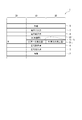
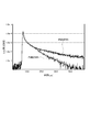
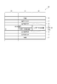
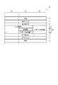
- FIG. 1 is a schematic view of an organic EL light emitting device according to a first embodiment. It is the schematic of the apparatus which measures transient PL. It is a figure which shows an example of the attenuation curve of transient PL. It is the schematic of the organic electroluminescent light emitting device which concerns on 2nd embodiment. It is the schematic of the organic electroluminescent light-emitting device which concerns on 3rd embodiment.
- FIG. 1 shows a schematic diagram of an organic EL light emitting device 1 according to the present embodiment.
- the organic EL light emitting device 1 includes a first pixel 10, a second pixel 20, and a third pixel 30.
- the organic EL light emitting device 1 includes a first pixel 10, a second pixel 20, and a third pixel 30 in parallel.
- the organic EL light emitting device 1 in which the first pixel 10 emits green light, the second pixel 20 emits blue light, and the third pixel 30 emits red light is taken as an example.
- the “pixel other than the second pixel” refers to a pixel having a configuration different from that of the second pixel.
- the first pixel and the third pixel are “other than the second pixel”.
- the “pixel other than the second pixel” is not limited to two types of pixels as in the present embodiment, and may be one type or three or more types.
- the organic EL light emitting device 1 includes an anode 2, a hole injection layer 3, a hole transport layer 4, a light emission zone 5, an electron transport layer 6, an electron injection layer 7, and a cathode 8.
- the anode 2, the hole injection layer 3, the hole transport layer 4, the emission band 5, the electron transport layer 6, the electron injection layer 7, and the cathode 8 are laminated in this order.
- the light emission band 5 is responsible for the light emission of the organic EL light emitting device 1.
- the configuration of the emission band 5 is different between the first pixel 10, the second pixel 20, and the third pixel 30.
- the emission band 5 has a common layer 50 containing a delayed fluorescent compound (sometimes referred to as a delayed fluorescent compound).
- the common layer 50 of the present embodiment is a layer provided in common across the first pixel 10, the second pixel 20, and the third pixel 30.
- the common layer 50 is a compound included in the non-common layer by transferring energy generated by excitation of the delayed fluorescent compound contained in the common layer 50 to the non-common layer of the first pixel 10 or the third pixel 30. Sensitize.
- the common layer 50 may further include a fluorescent compound (sometimes referred to as a first fluorescent compound).
- the emission band 5 of the first pixel 10 has a first emission layer 15 as a non-common layer between the hole transport layer 4 and the electron transport layer 6, and the first emission layer 15 and the electron transport.
- a common layer 50 is provided between the layers 6.
- the first light emitting layer 15 is in contact with the common layer 50.
- the compound contained in the first light emitting layer 15 is sensitized by receiving energy directly from the delayed fluorescent compound contained in the common layer 50 or via the first fluorescent light emitting compound.
- the first light emitting layer 15 includes a second fluorescent compound. When the common layer 50 in contact with the first light emitting layer 15 contains the delayed fluorescent compound, the second fluorescent compound can be efficiently emitted. That is, the light emission efficiency of the first pixel 10 can be improved.
- the emission band 5 of the second pixel 20 has a common layer 50.
- the second pixel 20 emits light from the common layer 50. Therefore, the common layer 50 in the second pixel also functions as a second light emitting layer in the organic EL light emitting device 1.
- the first fluorescent compound can be efficiently emitted. That is, the light emission efficiency of the second pixel 20 can be improved.
- the singlet energy of the delayed fluorescent compound is preferably larger than the singlet energy of the first fluorescent compound.
- the common layer 50 may further contain a third compound.
- the singlet energy of the third compound is preferably larger than the singlet energy of the delayed fluorescent compound.
- the singlet energy of the delayed fluorescent compound is larger than the singlet energy of the first fluorescent compound, and the singlet of the delayed fluorescent compound is further increased.
- the singlet energy of the third compound is preferably larger than the term energy.
- the emission band 5 of the third pixel 30 has a third emission layer 35 as a non-common layer between the hole transport layer 4 and the electron transport layer 6, and the third emission layer 35 and the electron transport layer.
- a common layer 50 is provided between the layers 6.
- the third light emitting layer 35 is in contact with the common layer 50.
- the compound contained in the third light emitting layer 35 is sensitized by receiving energy directly from the delayed fluorescent compound contained in the common layer 50 or via the first fluorescent compound.
- the third light emitting layer 35 includes a third fluorescent compound. Since the common layer 50 in contact with the third light emitting layer 35 contains the delayed fluorescent compound, the third fluorescent compound can be efficiently emitted. That is, the light emission efficiency of the third pixel 30 can be improved.
- the second pixel 20 exhibits light emission from the common layer 50
- the first pixel 10 exhibits light emission from the first light emitting layer 15 instead of light emission from the common layer 50
- the third pixel 30 also preferably emits light from the third light emitting layer 35 instead of light emitted from the common layer 50.
- the first pixel 10 may exhibit mixed color light emission of light emission from the common layer 50 and light emission from the first light emitting layer 15.
- the third pixel 30 may exhibit mixed light emission of light emission from the common layer 50 and light emission from the third light emitting layer 35.
- the peak wavelength of light emission from the common layer 50 is preferably smaller than the peak wavelength of light emission from the first light emitting layer 15 and the third light emitting layer 35 as non-common layers.
- the energy of the light emitting level of the delayed fluorescent compound contained in the common layer 50 is contained in the energy of the light emitting level of the compound contained in the first light emitting layer 15 as the non-common layer and the third light emitting layer 35. It is preferably larger than the energy of the emission level of the compound.
- Delayed fluorescence (thermally activated delayed fluorescence) is explained on pages 261 to 268 of “Device properties of organic semiconductors” (edited by Chiba Adachi, published by Kodansha).
- the energy difference ⁇ E 13 between the excited singlet state and the excited triplet state of the fluorescent material can be reduced, the reverse energy from the excited triplet state to the excited singlet state, which usually has a low transition probability. It is described that migration occurs with a high probability and that thermally activated delayed fluorescence (TADF) is expressed.
- FIG. 10.38 in this document explains the mechanism of delayed fluorescence generation.
- the delayed fluorescent compound in the present embodiment is a compound that exhibits thermally activated delayed fluorescence generated by such a mechanism.
- the delayed fluorescence emission can be confirmed by transient PL (Photo Luminescence) measurement.
- Transient PL measurement is a method of measuring the decay behavior (transient characteristics) of PL emission after irradiating a sample with a pulse laser and exciting it and stopping the irradiation.
- PL emission in the TADF material is classified into a light emission component from a singlet exciton generated by the first PL excitation and a light emission component from a singlet exciton generated via a triplet exciton.
- the lifetime of singlet excitons generated by the first PL excitation is on the order of nanoseconds and is very short. Therefore, light emitted from the singlet excitons is rapidly attenuated after irradiation with the pulse laser.
- delayed fluorescence is emitted slowly from singlet excitons generated via a long-lived triplet exciton, and thus slowly attenuates.
- the emission intensity derived from delayed fluorescence can be obtained.
- FIG. 2 shows a schematic diagram of an exemplary apparatus for measuring transient PL.
- the transient PL measurement apparatus 100 of the present embodiment includes a pulse laser unit 101 that can irradiate light of a predetermined wavelength, a sample chamber 102 that houses a measurement sample, a spectrometer 103 that separates light emitted from the measurement sample, A streak camera 104 for forming a two-dimensional image and a personal computer 105 for capturing and analyzing the two-dimensional image are provided. Note that the measurement of the transient PL is not limited to the apparatus described in this embodiment.
- the sample accommodated in the sample chamber 102 is obtained by forming a thin film in which a doping material is doped at a concentration of 12 mass% with respect to a matrix material on a quartz substrate.
- the thin film sample accommodated in the sample chamber 102 is irradiated with a pulse laser from the pulse laser unit 101 to excite the doping material.
- the emitted light is extracted in a direction of 90 degrees with respect to the irradiation direction of the excitation light, the extracted light is dispersed by the spectroscope 103, and a two-dimensional image is formed in the streak camera 104.
- a two-dimensional image in which the vertical axis corresponds to time, the horizontal axis corresponds to wavelength, and the bright spot corresponds to emission intensity.
- an emission spectrum in which the vertical axis represents the emission intensity and the horizontal axis represents the wavelength can be obtained.
- an attenuation curve in which the vertical axis represents the logarithm of the emission intensity and the horizontal axis represents time can be obtained.
- the thin film sample A was prepared as described above using the following reference compound M1 as a matrix material and the following reference compound DP1 as a doping material, and transient PL measurement was performed.
- FIG. 3 shows attenuation curves obtained from the transient PL measured for the thin film sample A and the thin film sample B.
- the transient PL measurement it is possible to obtain a light emission decay curve with the vertical axis representing the emission intensity and the horizontal axis representing the time. Based on this emission decay curve, the fluorescence intensity of fluorescence emitted from the singlet excited state generated by photoexcitation and delayed fluorescence emitted from the singlet excited state generated by reverse energy transfer via the triplet excited state The ratio can be estimated.
- the ratio of the delayed fluorescence intensity that gradually attenuates to the fluorescence intensity that decays quickly is somewhat large.
- the delayed fluorescence emission amount in this embodiment can be obtained using the apparatus of FIG.
- the delayed fluorescent compound is excited with pulsed light having a wavelength absorbed by the delayed fluorescent compound (light irradiated from a pulse laser) and then promptly observed from the excited state. After the excitation, there is delay light emission (delayed light emission) that is not observed immediately but is observed thereafter.
- the amount of delay light emission (delayed light emission) is preferably 5% or more with respect to the amount of Promp light emission (immediate light emission).
- the amounts of Prompt light emission and Delay light emission can be obtained by a method similar to the method described in “Nature 492, 234-238, 2012”.
- the apparatus used for calculation of the amount of Promp light emission and Delay light emission is not limited to the apparatus described in the said literature.
- a delayed fluorescent compound and the following compound TH-2 are co-deposited on a quartz substrate so that the ratio of the delayed fluorescent compound is 12% by mass.
- a sample in which a thin film having a thickness of 100 nm is formed can be used.
- -TADF mechanism It is preferable to use a compound having a small ⁇ ST (DF) as the delayed fluorescent compound, and from the triplet level of the delayed fluorescent compound to the singlet level of the delayed fluorescent compound by externally applied thermal energy. Inverse crossing is likely to occur.
- An energy state conversion mechanism in which the excited triplet state of the electrically excited exciton inside the organic EL element is spin-exchanged to the excited singlet state by crossing between inverse terms is called a TADF mechanism.
- the difference between the lowest excited singlet state S1 and the lowest excited triplet state T1 is defined as ⁇ ST.
- the common layer 50 in the emission band 5 of the second pixel 20 includes a delayed fluorescent compound.
- the common layer 50 in the emission band 5 of the second pixel 20 may further include a first fluorescent compound.
- a compound having a small ⁇ ST (DF) is used as the delayed fluorescent compound, the lowest excited triplet state T1 (DF) can cross to the lowest excited singlet state S1 (DF) by thermal energy. .
- DF small ⁇ ST
- DF forster type energy transfer occurs from the lowest excited singlet state S1 (DF) of the delayed fluorescent compound to the lowest excited singlet state S1 (M1) of the first fluorescent compound.
- fluorescence emission from the lowest excited singlet state S1 (M1) of the first fluorescent compound can be observed.
- the common layer 50 in the light emission band 5 of the first pixel 10 is in contact with the first light emitting layer 15, and the first light emitting layer 15 includes a second fluorescent compound. Therefore, a Forster type energy transfer from the lowest excited singlet state S1 (DF) of the delayed fluorescent compound to the lowest excited singlet state S1 (M2) of the second fluorescent compound occurs or the common layer 50 has Forster, from the lowest excited singlet state S1 (M1) of the first fluorescent compound to the lowest excited singlet state S1 (M2) of the second fluorescent compound when the first fluorescent compound is included Type energy transfer occurs. As a result, fluorescence emission from the lowest excited singlet state S1 (M2) of the second fluorescent compound can be observed.
- the singlet energy S (DF) of the delayed fluorescent compound is preferably larger than the singlet energy S (M2) of the second fluorescent compound.
- the common layer 50 in the light emission band 5 of the third pixel 30 is in contact with the third light emitting layer 35, and the third light emitting layer 35 contains a third fluorescent compound. Therefore, a Forster type energy transfer from the lowest excited singlet state S1 (DF) of the delayed fluorescent compound to the lowest excited singlet state S1 (M3) of the third fluorescent compound occurs, or the common layer 50 In the case of including the first fluorescent compound, Forster from the lowest excited singlet state S1 (M1) of the first fluorescent compound to the lowest excited singlet state S1 (M3) of the third fluorescent compound Type energy transfer occurs. As a result, fluorescence emission from the lowest excited singlet state S1 (M3) of the third fluorescent compound can be observed.
- the singlet energy S (DF) of the delayed fluorescent compound is preferably larger than the singlet energy S (M3) of the third fluorescent compound.
- the light emission efficiency can be improved. Furthermore, even in the organic EL light emitting device 1 having a plurality of pixels exhibiting different emission colors, it is only necessary to provide the common layer 50 in common across the respective pixels, so that the configuration and the manufacturing process can be simplified.
- an organic EL light emitting device including a fluorescent compound in a common layer, an organic EL light emitting device including a phosphorescent compound, and the like have been proposed. In these organic EL light emitting devices, energy is transferred from the common layer to the adjacent light emitting layer, and an attempt is made to improve the light emission efficiency by the sensitizing effect on the compound contained in the adjacent light emitting layer.
- the internal quantum yield can be increased to 100% by using a phosphorescent compound for the common layer.
- phosphorescence is a forbidden transition, the Förster radius (distance to which energy moves) is small, and there is a problem in energy transfer from the common layer to the light emitting layer.
- the fluorescence is an allowable transition, so that the Forster radius is large, and energy transfer from the common layer to the light emitting layer is easy.
- the EL internal quantum yield is 25%, there is a problem in luminous efficiency.
- the delayed fluorescent compound contained in the common layer 50 in the organic EL light emitting device 1 of the present embodiment can increase the internal quantum yield to 100%.
- delayed fluorescence is an allowable transition, the Forster radius is large, and energy is easily transferred from the common layer to the light emitting layer. Therefore, according to the organic EL light emitting device 1 of the present embodiment, the light emission efficiency can be improved.
- the organic EL light emitting device 1 of the present embodiment when the common layer 50 includes the first fluorescent compound, energy transfer from the delayed fluorescent compound to the first fluorescent compound in the common layer 50. happens. Further, since the emission rate constant of the first fluorescent compound is larger than the emission rate constant of the delayed fluorescent compound, the Forster radius is large, and the second fluorescent compound and the third fluorescent light are emitted from the common layer 50. Energy transfer to the active compound. Therefore, the organic EL light emitting device 1 is more preferable in terms of luminous efficiency.
- the first light emitting layer 15 and the third light emitting layer 35 each contain a fluorescent compound. Since the fluorescent compound has a higher extinction coefficient than the delayed fluorescent compound or the phosphorescent compound, it is easy to receive energy from the delayed fluorescent compound of the common layer 50. Therefore, the organic EL light emitting device 1 is more preferable in terms of luminous efficiency.
- the energy gap T 77K (DF) at 77 [K] of the delayed fluorescent compound is preferably larger than the energy gap T 77K (M1) at 77 [K] of the first fluorescent compound.
- T 77K (DF) is preferably 2.0 eV or more, and more preferably 2.2 eV or more.
- the energy gap at 77 [K] is different from the normally defined triplet energy.
- the triplet energy is measured as follows. First, a sample in which a compound to be measured is deposited on a quartz substrate or a sample in which a solution dissolved in an appropriate solvent is enclosed in a quartz glass tube is prepared.
- a phosphorescence spectrum (vertical axis: phosphorescence emission intensity, horizontal axis: wavelength) is measured at a low temperature (77 [K]), and a tangent line is drawn with respect to the rising edge on the short wavelength side of the phosphorescence spectrum, Based on the wavelength value at the intersection of the tangent and the horizontal axis, triplet energy is calculated from a predetermined conversion formula.
- the delayed fluorescent compound used in the present embodiment is preferably a compound having a small ⁇ ST. When ⁇ ST is small, intersystem crossing and reverse intersystem crossing easily occur even in a low temperature (77 [K]) state, and an excited singlet state and an excited triplet state are mixed.
- the spectrum measured in the same manner as described above includes light emission from both the excited singlet state and the excited triplet state, and it is difficult to distinguish clearly from which state the light is emitted.
- the triplet energy value is considered dominant. Therefore, in the present embodiment, the normal triplet energy T and the measurement method are the same, but in order to distinguish the difference in the strict meaning, the value measured as follows is referred to as an energy gap T 77K. .
- a sample is prepared by vapor-depositing a compound to be measured on a quartz substrate with a film thickness of 100 nm.
- the maximum point having a peak intensity of 15% or less of the maximum peak intensity of the spectrum is not included in the above-mentioned maximum value on the shortest wavelength side, and has the maximum slope value closest to the maximum value on the shortest wavelength side.
- the tangent drawn at the point where the value is taken is taken as the tangent to the rising edge of the phosphorescence spectrum on the short wavelength side.
- an F-4500 type spectrofluorometer main body manufactured by Hitachi High-Technology Co., Ltd. can be used.
- the measurement device is not limited to this, and the measurement may be performed by combining a cooling device and a cryogenic container, an excitation light source, and a light receiving device.
- the absorption spectrum is measured with a spectrophotometer. For example, a Hitachi spectrophotometer (device name: U3310) or the like can be used.
- a tangent to the rising edge of the emission spectrum on the short wavelength side is drawn as follows.
- tangents at each point on the curve are considered toward the long wavelength side.
- the slope of this tangent line increases as the curve rises (that is, as the vertical axis increases).
- the tangent drawn at the point where the value of the slope takes the maximum value is the tangent to the short wavelength side rise of the emission spectrum.
- the maximum point having a peak intensity of 15% or less of the maximum peak intensity of the spectrum is not included in the above-mentioned maximum value on the shortest wavelength side, and has the maximum slope value closest to the maximum value on the shortest wavelength side.
- the tangent drawn at the point where the value is taken is taken as the tangent to the rising edge of the emission spectrum on the short wavelength side.
- the cause may be the formation of molecular aggregates or strong interaction with the solvent. . Therefore, the above measurement can also be performed using a sample in which a compound to be measured and another appropriate material having a large energy gap and not forming an exciplex are co-deposited on a quartz substrate.
- the organic EL light emitting device 1 may further include a substrate as a support.
- a substrate for example, glass, quartz, plastic, or the like can be used as the substrate.
- a flexible substrate may be used.
- a flexible substrate is a substrate that can be bent (flexible). Examples of the flexible substrate include a plastic substrate made of polycarbonate or polyvinyl chloride.
- anode For the anode 2, it is preferable to use a metal, an alloy, an electrically conductive compound, a mixture thereof, or the like having a high work function (specifically, 4.0 eV or more).
- the material of the anode 2 include indium tin oxide (ITO), indium oxide-tin oxide containing silicon or silicon oxide, indium oxide-zinc oxide, tungsten oxide, and the like. Examples thereof include indium oxide containing zinc oxide and graphene.
- examples of the material of the anode 2 include gold (Au), platinum (Pt), or a metal nitride (for example, titanium nitride).
- the hole injection layer 3 is a layer containing a substance having a high hole injection property.
- substances having a high hole injection property include molybdenum oxide, titanium oxide, vanadium oxide, rhenium oxide, ruthenium oxide, chromium oxide, zirconium oxide, hafnium oxide, tantalum oxide, and silver oxide. Products, tungsten oxides, manganese oxides, aromatic amine compounds, and polymer compounds (oligomers, dendrimers, polymers, and the like).
- the hole transport layer 4 is a layer containing a substance having a high hole transport property.
- the compound used for the hole transport layer 4 include aromatic amine compounds, carbazole derivatives, and anthracene derivatives.
- a high molecular compound such as poly (N-vinylcarbazole) (abbreviation: PVK) or poly (4-vinyltriphenylamine) (abbreviation: PVTPA) can also be used for the hole transport layer 4.
- PVK N-vinylcarbazole
- PVTPA poly (4-vinyltriphenylamine
- compounds other than these may be used for the hole transport layer 4 as long as the substance has a property of transporting more holes than electrons.
- the layer containing a substance having a high hole-transport property may be a single layer or a stacked layer in which two or more layers including the above substances are stacked.
- the fluorescent compounds contained in the common layer 50, the first light emitting layer 15, and the third light emitting layer 35 are compounds that can emit light from a singlet excited state.
- the kind of fluorescent compound is not specifically limited.
- Examples of the fluorescent compounds that emit blue light include pyrene derivatives, styrylamine derivatives, chrysene derivatives, fluoranthene derivatives, fluorene derivatives, diamine derivatives, and triarylamine derivatives.
- Examples of the fluorescent compound that emits green light include a coumarin derivative, a pyromethene boron complex, and an aromatic amine derivative.
- Examples of the fluorescent compound that emits red light include a tetracene derivative, a perifuranthene derivative, a pyromethene boron complex, and a diamine derivative.
- the 1st light emitting layer 15 and the 3rd light emitting layer 35 are good also as a structure which disperse
- Various compounds can be used as the substance for dispersing the substance having high light-emitting properties.
- the host material it is preferable to use a substance having a lowest lowest orbital level (LUMO level) and a lower highest occupied orbital level (HOMO level) than a substance having high light-emitting properties.
- the substance (host material) for dispersing a substance having a high light emitting property include metal complexes, heterocyclic compounds, condensed aromatic compounds, and aromatic amine compounds.
- Examples of the metal complex include an aluminum complex, a beryllium complex, and a zinc complex.
- Examples of the heterocyclic compound include oxadiazole derivatives, benzimidazole derivatives, dibenzofuran derivatives, dibenzothiophene derivatives, azine derivatives, indole derivatives, carbazole derivatives, and phenanthroline derivatives.
- Examples of the condensed aromatic compound include anthracene derivatives, phenanthrene derivatives, triphenylene derivatives, pyrene derivatives, and chrysene derivatives.
- Examples of the aromatic amine compound include triarylamine derivatives and condensed polycyclic aromatic amine derivatives.
- the electron transport layer 6 is a layer containing a substance having a high electron transport property.
- the compound used for the electron transport layer 6 include metal complexes, heteroaromatic compounds, and polymer compounds.
- the metal complex include an aluminum complex, a beryllium complex, and a zinc complex.
- the heteroaromatic compound include imidazole derivatives, benzimidazole derivatives, azine derivatives, carbazole derivatives, and phenanthroline derivatives.
- the electron injection layer 7 is a layer containing a substance having a high electron injection property.
- the compound used for the electron injection layer 7 include alkali metals, alkaline earth metals, alkali metal compounds, and alkaline earth metal compounds.
- Specific examples of the compound used for the electron injection layer 7 include, for example, lithium (Li), lithium fluoride (LiF), cesium fluoride (CsF), calcium fluoride (CaF 2 ), and lithium oxide (LiOx).
- Etc As a metal complex, a lithium quinolinolato (LiQ) complex etc. are mentioned, for example.
- cathode For the cathode 8, it is preferable to use a metal, an alloy, an electrically conductive compound, a mixture thereof, or the like having a low work function (specifically, 3.8 eV or less).
- the compound used for the cathode 8 include elements belonging to Group 1 or Group 2 of the periodic table, ie, alkali metals such as lithium (Li) and cesium (Cs), and alkalis such as magnesium (Mg).
- alkali metals such as lithium (Li) and cesium (Cs)
- Mg magnesium
- earth metals, and alloys containing these for example, MgAg and AlLi
- rare earth metals such as europium (Eu), ytterbium (Yb), and alloys containing these.
- the film thickness of each layer of the organic EL light emitting device 1 is not limited except as specifically mentioned above. In general, if the film thickness is too thin, defects such as pinholes are likely to occur. Conversely, if the film thickness is too thick, a high applied voltage is required and the efficiency is deteriorated.
- the method for forming each layer of the organic EL light emitting device 1 is not limited to those described above, and a known method such as a dry film forming method or a wet film forming method can be employed.
- a dry film forming method include a vacuum deposition method, a sputtering method, a plasma method, and an ion plating method.
- the wet film forming method include a spin coating method, a dipping method, a flow coating method, and an ink jet method.
- the organic EL light emitting device 1 can be used for electronic devices such as a display device and a light emitting device.
- Examples of the display device include display components such as an organic EL panel module, a television, a mobile phone, a tablet, or a personal computer.
- Examples of the light emitting device include lighting or a vehicular lamp.
- FIG. 4 shows a schematic diagram of the organic EL light emitting device 1A according to the present embodiment.
- the common layer 51 is a layer provided in common across the first pixel 11 and the second pixel 21, and the third pixel 31 is the common layer 51. It is different from the organic EL light emitting device 1 of the first embodiment in that it is not in contact with. Other points are the same as in the first embodiment.
- the organic EL light emitting device 1A in which the first pixel 11 emits red light, the second pixel 21 emits blue light, and the third pixel 31 emits green light is taken as an example. explain.
- the emission band 5A of the organic EL light emitting device 1A has a common layer 51 containing a delayed fluorescent compound.
- the common layer 51 may further include a first fluorescent compound.
- the light emission band 5A of the first pixel 11 includes a first light emitting layer 15A as a non-common layer between the hole transport layer 4 and the electron transport layer 6, and the first light emitting layer 15A and the electron transport layer.
- a common layer 51 is provided between the layers 6.
- the first light emitting layer 15 ⁇ / b> A is in contact with the common layer 51.
- the first light emitting layer 15A includes the second fluorescent light emitting compound, the light emission efficiency of the first pixel 11 can be improved as described above.
- the emission band 5 ⁇ / b> A of the second pixel 21 has a common layer 51.
- the second pixel 21 emits light from the common layer 51.
- the common layer 51 contains a delayed fluorescent compound.
- the luminous efficiency of the second pixel 21 can be improved as described above.
- the singlet energy of the delayed fluorescent compound is preferably larger than the singlet energy of the first fluorescent compound.
- the emission band 5 ⁇ / b> A of the third pixel 31 has a third emission layer 35 ⁇ / b> A as a non-common layer between the hole transport layer 4 and the electron transport layer 6.
- the peak wavelength of light emission from the common layer 51 is preferably smaller than the peak wavelength of light emission from the first light emitting layer 15A as a non-common layer. By satisfying such a peak wavelength relationship, energy can be easily transferred from the common layer 51 to the first light emitting layer 15A.
- the energy of the emission level of the delayed fluorescent compound contained in the common layer 51 is preferably larger than the energy of the emission level of the compound contained in the first emission layer 15A as a non-common layer. By satisfying such a relationship of energy of the light emission levels, energy can be easily transferred from the common layer 51 to the first light emitting layer 15A.
- the luminous efficiency can also be improved by the organic EL light emitting device 1A of the present embodiment.
- FIG. 5 shows a schematic diagram of the organic EL light emitting device 1B according to the present embodiment.
- the common layer 52 is a layer provided in common across the first pixel 12 and the second pixel 22, and the third pixel 32 is the common layer 52.
- the first pixel 12 emits red light
- the second pixel 22 emits green light.
- the third pixel 32 emits blue light.
- Other points are the same as in the first embodiment.
- the light emission band 5B of the organic EL light emitting device 1B has a common layer 52 containing a delayed fluorescent compound.
- the common layer 52 may further include a first fluorescent compound.
- the singlet energy of the delayed fluorescent compound is preferably larger than the singlet energy of the first fluorescent compound.
- the emission band 5B of the first pixel 12 includes a first emission layer 15B as a non-common layer between the hole transport layer 4 and the electron transport layer 6, and the first emission layer 15B and the electron transport.
- a common layer 52 is provided between the layers 6.
- the first light emitting layer 15B includes a second fluorescent compound.
- the barrier layer 9 is further provided between the common layer 52 and the first light emitting layer 15B.
- the energy gap T 77K (BL) at 77 [K] of the compound included in the barrier layer 9 is greater than or equal to the energy gap T 77K (DF) at 77 [K] of the delayed fluorescent compound included in the common layer 52.
- T 77K (BL) of the compound included in the barrier layer 9 is more preferably larger than T 77K (DF) of the delayed fluorescent compound included in the common layer 52.
- T 77K (BL) of the compound included in the barrier layer 9 is more preferably larger than T 77K (DF) of the delayed fluorescent compound included in the common layer 52.
- the energy gap T 77K (BL) at 77 [K] of the compound included in the barrier layer 9 is 77 [K] of the second fluorescent compound included in the first light-emitting layer 15B as the non-common layer. It is preferable that it is more than energy gap T 77K (M2) in
- the singlet energy of the compound contained in the barrier layer 9 is preferably equal to or higher than the singlet energy of the second fluorescent compound, and more preferably larger than the singlet energy of the second fluorescent compound.
- the light emission band 5 ⁇ / b> B of the second pixel 22 has a common layer 52.
- the second pixel 22 emits light from the common layer 52.
- the common layer 52 includes a delayed fluorescent compound. Further, when the common layer 52 contains the first fluorescent compound, the luminous efficiency of the second pixel 22 can be improved as described above.
- the emission band 5B of the third pixel 32 has a third emission layer 35B as a non-common layer between the hole transport layer 4 and the electron transport layer 6.
- the peak wavelength of light emission from the common layer 52 is preferably smaller than the peak wavelength of light emission from the first light-emitting layer 15B as a non-common layer. By satisfying such a peak wavelength relationship, energy can be easily transferred from the common layer 52 to the first light emitting layer 15B.
- the energy of the emission level of the delayed fluorescent compound contained in the common layer 52 is preferably larger than the energy of the emission level of the compound contained in the first emission layer 15B as the non-common layer. By satisfying such a relationship of energy of light emission levels, energy can be easily transferred from the common layer 52 to the first light emitting layer 15B.
- the light emission efficiency can also be improved by the organic EL light emitting device 1B of the present embodiment.
- each pixel exhibits red, green, or blue light emission
- the present invention is not limited to such an aspect.
- Examples of other emission colors exhibited by the pixels include yellow, orange, light blue, purple, and white.
- organic EL light emitting device for example, in the organic EL light emitting device 1A of the second embodiment, a mode in which the first pixel emits green light and the third pixel emits red light is changed. Can be mentioned.
- the organic EL light-emitting device 1A of the second embodiment has a first pixel that emits red light, a second pixel that emits green light, and a third pixel that emits light.
- the aspect changed into the aspect which exhibits blue light emission is mentioned.
- a non-common layer may be provided between the common layer and the anode, or a non-common layer may be provided between the common layer and the cathode.
- the first light emitting layer as the non-common layer of the first pixel is provided between the electron transport layer and the common layer, and the non-common layer of the third pixel is used.
- the third light emitting layer may be provided between the hole transport layer and the common layer.
- the barrier layer may be provided in organic EL light emitting devices other than the third embodiment.
- the barrier layer is provided between the common layer and the non-common layer.
- a first barrier layer is provided between the first light emitting layer and the common layer as the non-common layer of the first pixel, and the third pixel is not common.
- a second barrier layer may be provided between the third light emitting layer as a layer and the common layer.
- the compounds contained in each barrier layer may be the same or different.
- the compound used for the barrier layer is appropriately selected according to the compound contained in the light emitting layer as a non-common layer in contact with the barrier layer and the delayed fluorescent compound contained in the common layer.
- the embodiment in which the light emitting layer as the non-common layer includes the fluorescent compound is described as an example, but the present invention is not limited to these embodiments.
- the light emitting layer as the non-common layer may contain a phosphorescent compound. Since the common layer contains the delayed fluorescent compound, energy transfer from the common layer to the layer containing the phosphorescent compound is easier than in the conventional organic EL light emitting device.
- a phosphorescent compound is a compound that can emit light from a triplet excited state.
- a metal complex such as an iridium complex, an osmium complex, and a platinum complex is used.
- Examples of the phosphorescent compound that emits green light include iridium complexes and terbium complexes.
- a metal complex such as an iridium complex, a platinum complex, and a europium complex is used.
- the light emitting layer may contain a phosphorescent compound and the host material described above.
- the light-emitting compound contained in the light-emitting layer that is in direct contact with the common layer or indirectly through a barrier layer or the like may be the same light-emitting type or a different light-emitting type in each pixel.
- the first light emitting layer of the first pixel contains a phosphorescent light emitting compound
- the third light emitting layer of the third pixel contains a fluorescent light emitting compound.
- An embodiment in which the phosphorescent compound is contained in the first light emitting layer and a phosphorescent compound is contained in the third light emitting layer may be employed.
- the light emitting layer as the non-common layer may also contain a delayed fluorescent compound.
- the light emitting layer contains a delayed fluorescent compound and a fluorescent compound.
- the configuration of the light emission band of the organic EL light emitting device is not limited to the example of the embodiment.
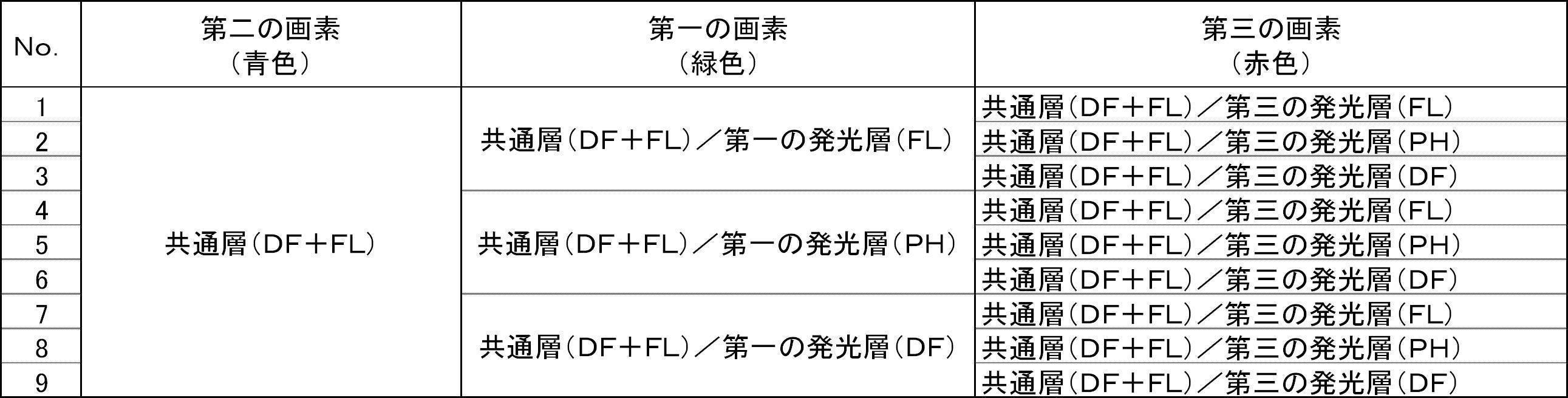
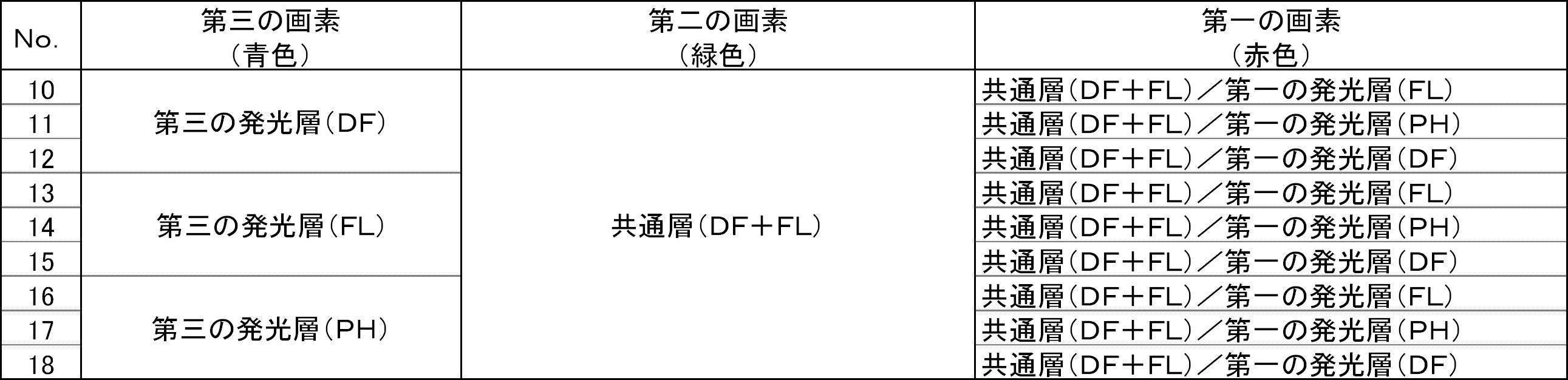
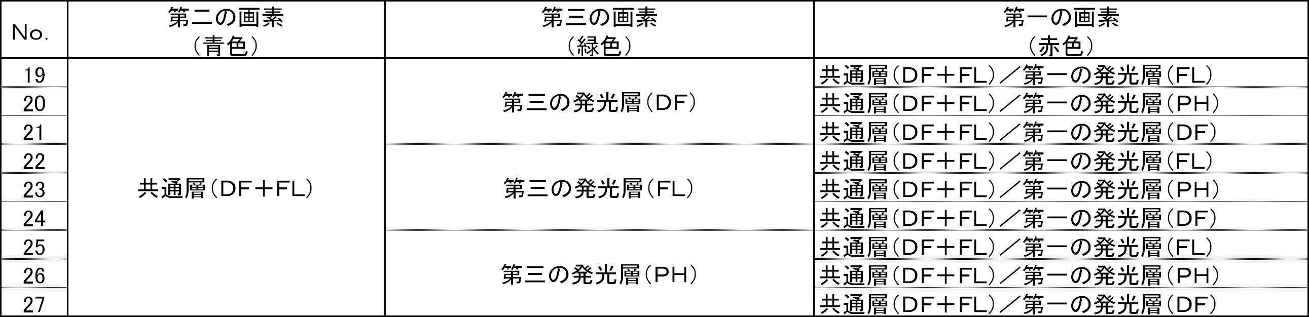
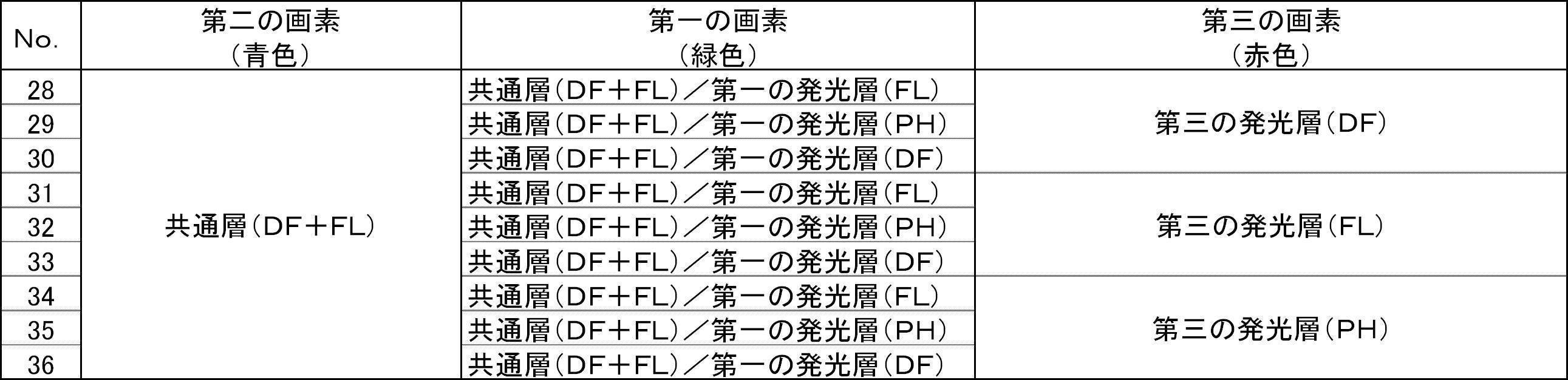
- the emission bands are Nos. 1 to 36 may be adopted.
- DF represents a delayed fluorescent compound
- FL represents a fluorescent compound
- PH represents a phosphorescent compound.
- the common layer provided in common across the first, second, and third pixels indicates DF + FL, that is, includes a delayed fluorescent compound and a fluorescent compound. . It shows that the first light emitting layer and the third light emitting layer contain FL, that is, a fluorescent compound.
- even the same symbol may indicate different compounds. For example, no.
- the fluorescent compound FL included in the first light emitting layer and the fluorescent compound FL included in the third light emitting layer may be different compounds. Further, in the layer configuration of each pixel, the stacked configuration is indicated by “/” like common layer / light emitting layer. In Tables 1 to 4, the stacked structure may be directly stacked, or a barrier layer may be included between the common layer and the light emitting layer. In Tables 1 to 4, the configuration of the “common layer (DF + FL)” is exemplified as the common layer. However, the present invention is not limited to these embodiments, and the configuration of the configuration that does not include the fluorescent compound FL. Common layer (DF) "may be used.
- the configurations of the “first light emitting layer (DF)” and the “third light emitting layer (DF)” are exemplified as the first light emitting layer or the third light emitting layer.
- the present invention is not limited to these embodiments, and may be a “first light-emitting layer (DF + FL)” or a “third light-emitting layer (DF + FL)” including the fluorescent compound FL.
- the organic EL light emitting device may include a color conversion device that converts the color of light emitted from each pixel.
- Examples of the color conversion device include a color filter. For example, when the light emission of the first pixel is a mixed color of the light emission from the common layer and the light emission from the light emission layer, the light emission from the common layer is blocked by providing a color conversion device in the organic EL light emission device. The light emitted from the light emitting layer can be transmitted.
- the light emitting layer is not limited to one layer, and a plurality of light emitting layers may be laminated.
- one pixel has a plurality of light-emitting layers, it is preferable that at least one light-emitting layer is in direct contact with the common layer or indirectly through a barrier layer or the like.
- the plurality of light emitting layers included in one pixel may be the same light emitting type or different light emitting types.
- the plurality of light emitting layers included in one pixel may be provided adjacent to each other, or may have a so-called tandem stacked structure in which a plurality of light emitting units are stacked via an intermediate layer.
- a block layer is provided adjacently between the light emitting layer and the electron transport layer, or between the light emitting layer and the hole transport layer. May be.
- the block layer is preferably disposed in contact with the light emitting layer and blocks at least one of holes, electrons, and excitons.
- a light emitting layer is provided between the common layer and the hole transport layer, it is preferable to provide a first block layer between the light emitting layer and the hole transport layer.
- a second block layer between the light emitting layer and the electron transport layer.
- the first block layer transports holes, and electrons are on the anode side of the first block layer (for example, a hole transport layer). Stop reaching.
- the organic EL light-emitting device has a second block layer
- the second block layer transports electrons, and holes are transferred to a layer on the cathode side of the second block layer (for example, an electron transport layer). Stop reaching.
- at least one of the first block layer and the second block layer may be adjacent to the light emitting layer so that excitation energy does not leak from the light emitting layer to the peripheral layer.
- the excitons generated in the light emitting layer are prevented from moving to a layer (for example, an electron transport layer or a hole transport layer) closer to the electrode than the block layer.
- the light emitting layer and the block layer are preferably joined.
- the pixels may be separated from each other while providing a common layer so that each pixel can emit light independently.
- the anode may be separated for each pixel, the layer structure from the anode to the hole transport layer or the light emitting layer may be separated for each pixel, or the layer structure from the electron transport layer to the cathode may be separated.
- the cathode may be separated for each pixel.
- An insulating film or the like may be interposed between the separated pixels.
- a thin film transistor for driving each pixel is formed on the substrate, and further, a pixel electrode (anode) corresponding to each pixel is formed, and each of the above layers is formed on the pixel electrode. You may let them.
- the organic EL light emitting device in which three or more types of pixels are provided in parallel has been described as an example.
- the organic EL light emitting device in which two types of pixels are provided in parallel may be.
- the organic EL light emitting device may include a plurality of sets of two or more types of pixels.
- an organic EL light emitting device including a plurality of sets of three types of pixels of a first pixel, a second pixel, and a third pixel may be used.
- the organic EL light-emitting device of the present invention is not limited to the organic EL light-emitting device of the first embodiment, and can be used for electronic devices.
- the delayed fluorescence was confirmed by measuring transient PL using the apparatus shown in FIG.
- the compound DF and the compound TH-2 were co-evaporated on a quartz substrate so that the ratio of the compound DF was 12% by mass, and a thin film having a thickness of 100 nm was formed to prepare a sample.
- Prompt light emission immediately observed from the excited state after excitation with pulsed light (light emitted from a pulsed laser) absorbed by the compound DF, and observation immediately after the excitation There is a delay light emission (delayed light emission) that is not observed.
- the delayed fluorescence in the present example means that the amount of delay light emission (delayed light emission) is 5% or more with respect to the amount of Promp light emission (immediate light emission).
- the amount of delay luminescence (delayed luminescence) was 5% or more with respect to the amount of Prompt luminescence (immediate luminescence).
- the amounts of Prompt light emission and Delay light emission can be obtained by a method similar to the method described in “Nature 492, 234-238, 2012”.
- the apparatus used for calculation of the amount of Promp light emission and Delay light emission is not limited to the apparatus of FIG. 2, or the apparatus described in literature.
- the energy of the emission level of each compound is as follows. The energy of the emission level of each compound is measured according to the method for measuring singlet energy described above.
- Compound DF 2.73 eV
- Compound GD 2.44 eV
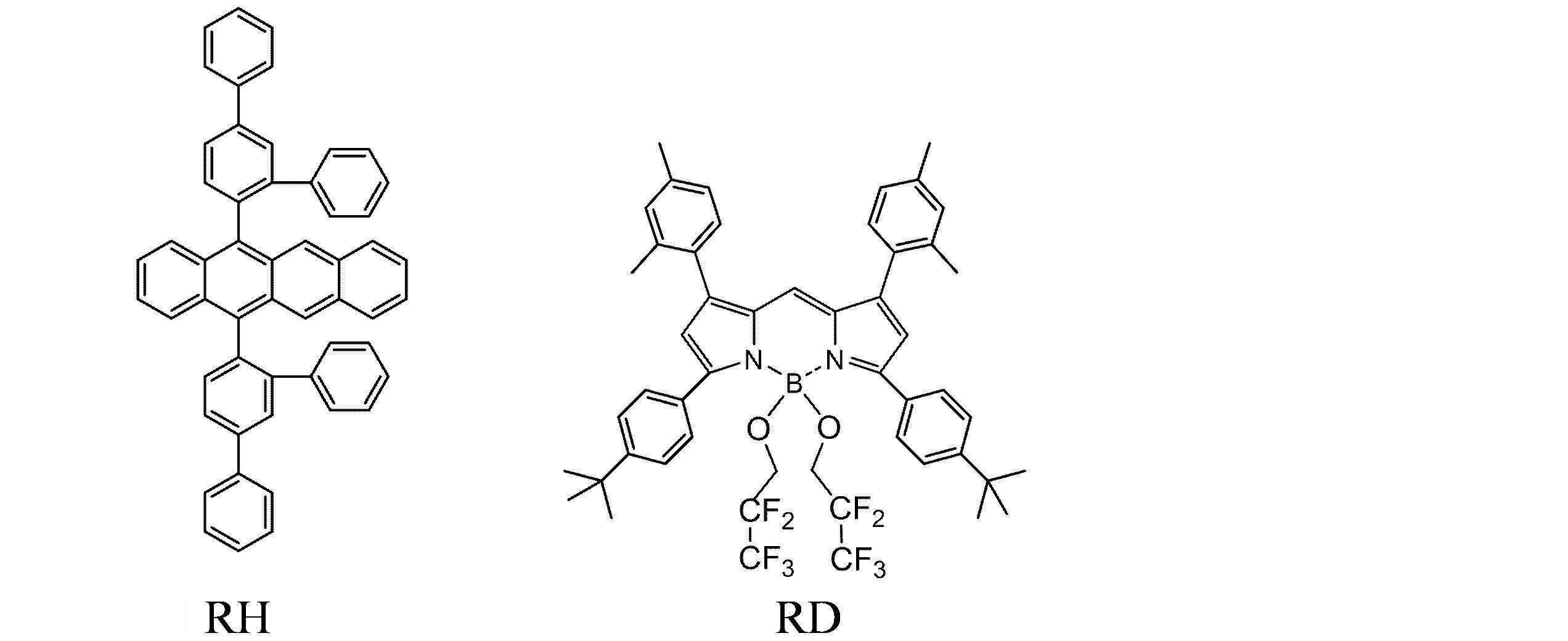
- Compound RD 2.00 eV
- Table 5 briefly shows configurations of the first pixel (R) and the second pixel (G) in the organic EL light emitting devices of Examples 1 and 2.
- the second pixel (G) has the same configuration.
- the organic EL light emitting devices of Examples 1 and 2 were provided with a common layer (G) in common.
- Table 6 briefly shows the configuration of the pixel (R) in the organic EL light emitting device of Comparative Example 1.
- the organic EL light emitting device of Comparative Example 1 was provided with a common layer not containing the compound DF.
- An organic EL light emitting device was produced as follows.
- Example 1 A glass substrate (manufactured by Geomatic Co., Ltd.) with an ITO transparent electrode (anode) having a thickness of 25 mm ⁇ 75 mm ⁇ 1.1 mm was subjected to ultrasonic cleaning for 5 minutes in isopropyl alcohol, and then UV ozone cleaning was performed for 30 minutes. The film thickness of ITO was 130 nm.
- the glass substrate with a transparent electrode line after washing was mounted on a substrate holder of a vacuum deposition apparatus. First, the compound HI was vapor-deposited so as to cover the transparent electrode on the surface where the transparent electrode line was formed, and the hole injection layers of the first pixel (R) and the second pixel (G) were formed. .
- the thickness of the hole injection layer was 5 nm.
- the compound HT1 was vapor-deposited on the hole injection layer, and the first hole transport layers of the first pixel (R) and the second pixel (G) were formed on the HI film.
- the film thickness of the first hole transport layer was 80 nm.
- the compound HT2 was deposited on the first hole transport layer of the second pixel (G) to form a second hole transport layer.
- the film thickness of the second hole transport layer was 10 nm.
- the compound HT2 was vapor-deposited on the first hole transport layer of the first pixel (R) to form a second hole transport layer.
- the film thickness of the second hole transport layer was 5 nm.
- the compound RH and the compound RD were co-evaporated on the second hole transport layer to form the first light emitting layer (R).
- the film thickness of the first light emitting layer (R) was 5 nm.
- the concentration of the compound RD in the first light emitting layer (R) was 1% by mass.
- the compound DA, the compound DF, Compound GD was co-evaporated to form a common layer (G) extending in common to the first pixel (R) and the second pixel (G).
- the concentration of compound DF in the common layer (G) was 50 mass%, and the concentration of compound GD was 1 mass%.
- the film thickness of the common layer (G) was 5 nm.
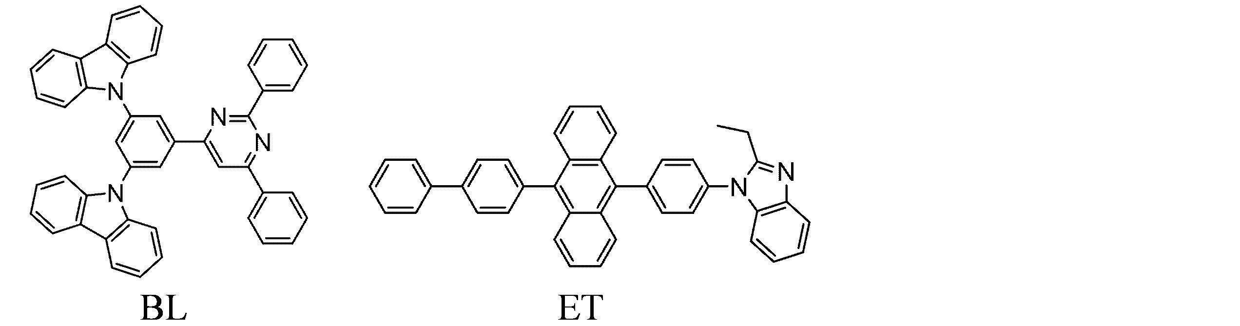
- the compound BL was vapor-deposited on the common layer (G) of the first pixel (R) and the second pixel (G) to form a block layer having a thickness of 5 nm.
- the compound ET was vapor-deposited on the block layers of the first pixel (R) and the second pixel (G) to form an electron transport layer having a thickness of 20 nm.
- lithium fluoride (LiF) was deposited on the electron transport layers of the first pixel (R) and the second pixel (G) to form an electron injection layer having a thickness of 1 nm.
- metal aluminum (Al) was vapor-deposited on the electron injection layer of the 1st pixel (R) and the 2nd pixel (G), and the cathode with a film thickness of 80 nm was formed.
- a configuration of the organic EL light emitting device of Example 1 is schematically shown as follows.
- the numbers in parentheses indicate the film thickness (unit: nm). Similarly, in the parentheses, the number displayed as a percentage indicates the ratio (% by mass) of the compound contained in the layer.
- Example 2 In the organic EL light emitting device of Example 2, the second pixel (G) is the same as that of Example 1, and the first pixel (R) is different from Example 1 in the following points.
- compound HT2 On the first light emitting layer (R) of the first pixel (R), compound HT2 was deposited to form a barrier layer. The thickness of the barrier layer was 1 nm.
- the configuration from the common layer (G) stacked on the barrier layer to the cathode is the same as that of the first pixel (R) in the first embodiment.
- a configuration of the first pixel (R) in the organic EL light emitting device of Example 2 is schematically shown as follows.
- the organic EL light emitting device of Comparative Example 1 does not include DF in the common layer (G) in the first pixel (R) of Example 1, and does not include the second pixel (G). This is different from the organic EL light emitting device of Example 1.
- the configuration of the organic EL light emitting device of Comparative Example 1 is schematically shown as follows. First pixel (R): ITO (130) / HI (5) / HT1 (80) / HT2 (5) / RH: RD (5, RD: 1%) / DA: GD (5, GD: 1% ) / BL (5) / ET (20) / LiF (1) / Al (80)
- Peak wavelength ⁇ p The peak wavelength ⁇ p was determined from the obtained spectral radiance spectrum.
- the peak wavelength ⁇ p (R) from the first pixel (R) was 620 nm.
- the peak wavelength ⁇ p (G) of light emission from the second pixel (G) was 532 nm.
- the luminance-current efficiency is higher than that of the organic EL light emitting device of Comparative Example 1 in which the common layer does not contain DF. Improved by 2.2 to 2.3 times.
- the luminance-current efficiency (L / J) was improved as compared with Example 1.
Landscapes
- Physics & Mathematics (AREA)
- Optics & Photonics (AREA)
- Electroluminescent Light Sources (AREA)
- Devices For Indicating Variable Information By Combining Individual Elements (AREA)
Abstract
Description
例えば、特許文献1には、赤、緑、青の各透明画素電極が形成され、赤と緑の透明画素電極上のみに赤色と緑色それぞれの有機発光層が形成され、さらに全面に青色の発光層が形成され、さらにこれらの上層に対向電極が形成されている有機EL発光装置が記載されている。特許文献1に記載の有機EL発光装置において、各色の発光層には、蛍光発光性の化合物が含まれる。
本発明の一態様に係る電子機器は、前述の本発明の一態様に係る有機EL発光装置を備える。
図1には、本実施形態に係る有機EL発光装置1の概略図が示されている。
有機EL発光装置1は、第一の画素10、第二の画素20、および第三の画素30を有する。本実施形態では、有機EL発光装置1は、第一の画素10、第二の画素20、および第三の画素30を並列に有する。本実施形態では、第一の画素10が緑色の発光を呈し、第二の画素20が青色の発光を呈し、第三の画素30が赤色の発光を呈する有機EL発光装置1を例に挙げて説明する。「第二の画素以外の画素」とは、第二の画素とは構成の異なる画素をいい、例えば、本実施形態では、第一の画素、および第三の画素が「第二の画素以外の画素」に相当する。「第二の画素以外の画素」は、本実施形態のように2種類の画素に限定されず、1種類でもよいし、3種類以上であってもよい。
共通層50は、さらに第三の化合物を含んでいてもよい。第三の化合物の一重項エネルギーは、遅延蛍光性化合物の一重項エネルギーよりも大きいことが好ましい。共通層50が第一の蛍光発光性化合物を含んでいる場合は、第一の蛍光発光性化合物の一重項エネルギーよりも、遅延蛍光性化合物の一重項エネルギーが大きく、さらに遅延蛍光性化合物の一重項エネルギーよりも第三の化合物の一重項エネルギーが大きいことが好ましい。
遅延蛍光(熱活性化遅延蛍光)については、「有機半導体のデバイス物性」(安達千波矢編、講談社発行)の261~268ページで解説されている。その文献の中で、蛍光発光材料の励起一重項状態と励起三重項状態のエネルギー差ΔE13を小さくすることができれば、通常は遷移確率が低い励起三重項状態から励起一重項状態への逆エネルギー移動が高確率で生じ、熱活性化遅延蛍光(Thermally Activated delayed Fluorescence, TADF)が発現すると説明されている。さらに、当該文献中の図10.38で、遅延蛍光の発生メカニズムが説明されている。本実施形態における遅延蛍光性化合物は、このようなメカニズムで発生する熱活性化遅延蛍光を示す化合物である。遅延蛍光の発光は過渡PL(Photo Luminescence)測定により確認できる。
一方、遅延蛍光は、寿命の長い三重項励起子を経由して生成する一重項励起子からの発光であるため、ゆるやかに減衰する。このように最初のPL励起で生成する一重項励起子からの発光と、三重項励起子を経由して生成する一重項励起子からの発光とでは、時間的に大きな差がある。そのため、遅延蛍光由来の発光強度を求めることができる。
本実施形態の過渡PL測定装置100は、所定波長の光を照射可能なパルスレーザー部101と、測定試料を収容する試料室102と、測定試料から放射された光を分光する分光器103と、2次元像を結像するためのストリークカメラ104と、2次元像を取り込んで解析するパーソナルコンピュータ105と、を備える。なお、過渡PLの測定は、本実施形態で説明する装置に限定されない。
試料室102に収容される試料は、マトリックス材料に対し、ドーピング材料が12質量%の濃度でドープされた薄膜を石英基板に成膜することで得られる。
試料室102に収容された薄膜試料に対し、パルスレーザー部101からパルスレーザーを照射して、ドーピング材料を励起させる。励起光の照射方向に対して90度の方向へ発光を取り出し、取り出した光を分光器103で分光し、ストリークカメラ104内で2次元像を結像する。その結果、縦軸が時間に対応し、横軸が波長に対応し、輝点が発光強度に対応する2次元画像を得ることができる。この2次元画像を所定の時間軸で切り出すと、縦軸が発光強度であり、横軸が波長である発光スペクトルを得ることができる。また、当該2次元画像を波長軸で切り出すと、縦軸が発光強度の対数であり、横軸が時間である減衰曲線(過渡PL)を得ることができる。

図3には、薄膜試料Aおよび薄膜試料Bについて測定した過渡PLから得た減衰曲線が示されている。

本実施形態における遅延蛍光発光量は、図2の装置を用いて求めることができる。前記遅延蛍光性化合物は、当該遅延蛍光性化合物が吸収する波長のパルス光(パルスレーザーから照射される光)で励起された後、当該励起状態から即座に観察されるPrompt発光(即時発光)と、当該励起後、即座には観察されず、その後観察されるDelay発光(遅延発光)とが存在する。本実施形態においては、Delay発光(遅延発光)の量がPrompt発光(即時発光)の量に対して5%以上であることが好ましい。
Prompt発光とDelay発光の量は、“Nature 492, 234-238, 2012”に記載された方法と同様の方法により求めることができる。なお、Prompt発光およびDelay発光の量の算出に使用される装置は、前記文献に記載の装置に限定されない。
また、遅延蛍光性の測定に用いられる試料は、例えば、遅延蛍光性化合物と下記化合物TH-2とを、遅延蛍光性化合物の割合が12質量%となるように石英基板の上に共蒸着し、膜厚100nmの薄膜を形成した試料を使用することができる。

遅延蛍光性化合物としてΔST(DF)が小さい化合物を用いることが好ましく、外部から与えられる熱エネルギーによって、遅延蛍光性化合物の三重項準位から遅延蛍光性化合物の一重項準位への逆項間交差が起こり易くなる。有機EL素子内部の電気励起された励起子の励起三重項状態が、逆項間交差によって、励起一重項状態へスピン交換がされるエネルギー状態変換機構をTADF機構と呼ぶ。最低励起一重項状態S1と最低励起三重項状態T1との差を、ΔSTとして定義する。
従来、共通層に蛍光発光性の化合物を含む有機EL発光装置や、燐光発光性の化合物を含む有機EL発光装置などが提案されている。これらの有機EL発光装置では、共通層から近接する発光層へエネルギー移動させ、近接する発光層に含まれる化合物への増感効果によって、発光効率を向上させることを試みている。
例えば、共通層に燐光発光性の化合物を用いることで、内部量子収率を100%まで高めることができる。しかしながら、燐光は禁制遷移であるため、フェルスター半径(エネルギーが移動する距離)が小さく、共通層から発光層へのエネルギー移動において課題がある。
また、共通層に蛍光発光性の化合物を用いた場合、蛍光は許容遷移であるため、フェルスター半径は大きく、共通層から発光層へエネルギー移動し易い。しかしながら、EL内部量子収率は、25%であるため、発光効率において課題がある。
本実施形態の有機EL発光装置1で共通層50に含まれる遅延蛍光性化合物は、内部量子収率を100%まで高めることができると考えられる。さらに、遅延蛍光は許容遷移であるためフェルスター半径が大きく、共通層から発光層へエネルギー移動し易い。ゆえに、本実施形態の有機EL発光装置1によれば、発光効率を向上させることができる。
ここで、三重項エネルギーと77[K]におけるエネルギーギャップとの関係について説明する。本実施形態では、77[K]におけるエネルギーギャップは、通常定義される三重項エネルギーとは異なる点がある。
三重項エネルギーの測定は、次のようにして行われる。まず、測定対象となる化合物を石英基板上に蒸着した試料、または適切な溶媒中に溶解した溶液を石英ガラス管内に封入した試料を作製する。この試料について、低温(77[K])で燐光スペクトル(縦軸:燐光発光強度、横軸:波長とする。)を測定し、この燐光スペクトルの短波長側の立ち上がりに対して接線を引き、その接線と横軸との交点の波長値に基づいて、所定の換算式から三重項エネルギーを算出する。
ここで、本実施形態に用いる遅延蛍光性化合物としては、ΔSTが小さい化合物であることが好ましい。ΔSTが小さいと、低温(77[K])状態でも、項間交差、及び逆項間交差が起こりやすく、励起一重項状態と励起三重項状態とが混在する。その結果、上記と同様にして測定されるスペクトルは、励起一重項状態および励起三重項状態の両者からの発光を含んでおり、いずれの状態から発光したのかについて峻別することは困難であるが、基本的には三重項エネルギーの値が支配的と考えられる。
そのため、本実施形態では、通常の三重項エネルギーTと測定手法は同じであるが、その厳密な意味において異なることを区別するため、次のようにして測定される値をエネルギーギャップT77Kと称する。薄膜を用いて測定する場合には、測定対象となる化合物を石英基板上に膜厚100nmで蒸着して試料を作製する。この試料について、低温(77[K])で燐光スペクトル(縦軸:燐光発光強度、横軸:波長とする。)を測定し、この燐光スペクトルの短波長側の立ち上がりに対して接線を引き、その接線と横軸との交点の波長値λedge[nm]に基づいて、次の換算式(F1)から算出されるエネルギー量をエネルギーギャップT77Kとする。
換算式(F1):T77K[eV]=1239.85/λedge
燐光スペクトルの短波長側の立ち上がりに対する接線は以下のように引く。燐光スペクトルの短波長側から、スペクトルの極大値のうち、最も短波長側の極大値までスペクトル曲線上を移動する際に、長波長側に向けて曲線上の各点における接線を考える。この接線は、曲線が立ち上がるにつれ(つまり縦軸が増加するにつれ)、傾きが増加する。この傾きの値が極大値をとる点において引いた接線(すなわち変曲点における接線)が、当該燐光スペクトルの短波長側の立ち上がりに対する接線とする。
なお、スペクトルの最大ピーク強度の15%以下のピーク強度をもつ極大点は、上述の最も短波長側の極大値には含めず、最も短波長側の極大値に最も近い、傾きの値が極大値をとる点において引いた接線を当該燐光スペクトルの短波長側の立ち上がりに対する接線とする。
燐光の測定には、(株)日立ハイテクノロジー製のF-4500形分光蛍光光度計本体を用いることができる。なお、測定装置はこの限りではなく、冷却装置及び低温用容器と、励起光源と、受光装置とを組み合わせることにより、測定してもよい。
一重項エネルギーSは、次のようにして測定される。
測定対象となる化合物を石英基板上に膜厚100nmで蒸着して試料を作製し、常温(300K)でこの試料の発光スペクトル(縦軸:発光強度、横軸:波長とする。)を測定する。この発光スペクトルの短波長側の立ち上がりに対して接線を引き、その接線と横軸との交点の波長値λedge[nm]に基づいて、次に示す換算式(F2)から算出される。
換算式(F2):S[eV]=1239.85/λedge
吸収スペクトルは、分光光度計で測定する。例えば、日立社製の分光光度計(装置名:U3310)等を用いることができる。
なお、スペクトルの最大ピーク強度の15%以下のピーク強度をもつ極大点は、上述の最も短波長側の極大値には含めず、最も短波長側の極大値に最も近い、傾きの値が極大値をとる点において引いた接線を当該発光スペクトルの短波長側の立ち上がりに対する接線とする。
なお、石英基板上に蒸着した試料を用いた測定結果と、溶液を用いた測定結果とが大きく異なる場合には、その原因として分子の会合体の形成や溶媒との強い相互作用などが考えられる。そのため、測定対象となる化合物と、エネルギーギャップが大きくエキサイプレックスを形成しない適切な他の材料とを、石英基板上に共蒸着した試料を用いて上記の測定を行うこともできる。
有機EL発光装置1は、支持体としての基板をさらに有していてもよい。基板としては、例えば、ガラス、石英、プラスチックなどを用いることができる。また、可撓性基板を用いてもよい。可撓性基板とは、折り曲げることができる(フレキシブル)基板のことである。可撓性基板としては、例えば、ポリカーボネートやポリ塩化ビニルからなるプラスチック基板等が挙げられる。
陽極2には、仕事関数の大きい(具体的には4.0eV以上)金属、合金、電気伝導性化合物、およびこれらの混合物などを用いることが好ましい。陽極2の材質としては、具体的には、例えば、酸化インジウム-酸化スズ(ITO:Indium Tin Oxide)、珪素若しくは酸化珪素を含有した酸化インジウム-酸化スズ、酸化インジウム-酸化亜鉛、酸化タングステン、および酸化亜鉛を含有した酸化インジウム、グラフェン等が挙げられる。この他、陽極2の材質としては、金(Au)、白金(Pt)、または金属材料の窒化物(例えば、窒化チタン)等が挙げられる。
正孔注入層3は、正孔注入性の高い物質を含む層である。正孔注入性の高い物質としては、例えば、モリブデン酸化物、チタン酸化物、バナジウム酸化物、レニウム酸化物、ルテニウム酸化物、クロム酸化物、ジルコニウム酸化物、ハフニウム酸化物、タンタル酸化物、銀酸化物、タングステン酸化物、マンガン酸化物、芳香族アミン化合物、および高分子化合物(オリゴマー、デンドリマー、ポリマー等)等が挙げられる。
正孔輸送層4は、正孔輸送性の高い物質を含む層である。正孔輸送層4に用いられる化合物としては、例えば、芳香族アミン化合物、カルバゾール誘導体、およびアントラセン誘導体等が挙げられる。ポリ(N-ビニルカルバゾール)(略称:PVK)やポリ(4-ビニルトリフェニルアミン)(略称:PVTPA)等の高分子化合物を正孔輸送層4に用いることもできる。但し、電子よりも正孔の輸送性の高い物質であれば、これら以外の化合物を正孔輸送層4に用いてもよい。なお、正孔輸送性の高い物質を含む層は、単層であってもよいし、上記物質からなる層が二層以上積層された積層であってもよい。
共通層50、第一の発光層15および第三の発光層35に含まれる蛍光発光性化合物は、一重項励起状態から発光可能な化合物である。蛍光発光性化合物の種類は特に限定されない。青色の発光を呈する蛍光発光性化合物としては、例えば、ピレン誘導体、スチリルアミン誘導体、クリセン誘導体、フルオランテン誘導体、フルオレン誘導体、ジアミン誘導体、およびトリアリールアミン誘導体等が挙げられる。緑色の発光を呈する蛍光発光性化合物としては、例えば、クマリン誘導体、ピロメテンホウ素錯体、および芳香族アミン誘導体等が挙げられる。赤色の発光を呈する蛍光発光性化合物としては、例えば、テトラセン誘導体、ペリフランテン誘導体、ピロメテンホウ素錯体およびジアミン誘導体等が挙げられる。
発光性の高い物質を分散させるための物質(ホスト材料)としては、例えば、金属錯体、複素環化合物、縮合芳香族化合物、および芳香族アミン化合物が挙げられる。金属錯体としては、例えば、アルミニウム錯体、ベリリウム錯体、および亜鉛錯体等が挙げられる。複素環化合物としては、例えば、オキサジアゾール誘導体、ベンゾイミダゾール誘導体、ジベンゾフラン誘導体、ジベンゾチオフェン誘導体、アジン誘導体、インドール誘導体、カルバゾール誘導体、およびフェナントロリン誘導体等が挙げられる。縮合芳香族化合物としては、例えば、アントラセン誘導体、フェナントレン誘導体、トリフェニレン誘導体、ピレン誘導体、およびクリセン誘導体等が挙げられる。芳香族アミン化合物としては、例えば、トリアリールアミン誘導体、および縮合多環芳香族アミン誘導体等が挙げられる。
電子輸送層6は、電子輸送性の高い物質を含む層である。電子輸送層6に用いられる化合物としては、例えば、金属錯体、複素芳香族化合物、および高分子化合物等が挙げられる。金属錯体としては、例えば、アルミニウム錯体、ベリリウム錯体、および亜鉛錯体等が挙げられる。複素芳香族化合物としては、例えば、イミダゾール誘導体、ベンゾイミダゾール誘導体、アジン誘導体、カルバゾール誘導体、およびフェナントロリン誘導体等が挙げられる。
電子注入層7は、電子注入性の高い物質を含む層である。電子注入層7に用いられる化合物としては、例えば、アルカリ金属、アルカリ土類金属、アルカリ金属化合物、およびアルカリ土類金属化合物等が挙げられる。電子注入層7に用いられる化合物の具体例としては、例えば、リチウム(Li)、フッ化リチウム(LiF)、フッ化セシウム(CsF)、フッ化カルシウム(CaF2)、およびリチウム酸化物(LiOx)等が挙げられる。金属錯体としては、例えば、リチウムキノリノラト(LiQ)錯体などが挙げられる。
陰極8には、仕事関数の小さい(具体的には3.8eV以下)金属、合金、電気伝導性化合物、およびこれらの混合物などを用いることが好ましい。陰極8に用いられる化合物の具体例としては、元素周期表の第1族または第2族に属する元素、すなわちリチウム(Li)やセシウム(Cs)等のアルカリ金属、およびマグネシウム(Mg)等のアルカリ土類金属、およびこれらを含む合金(例えば、MgAgやAlLi)、ユーロピウム(Eu)、イッテルビウム(Yb)等の希土類金属およびこれらを含む合金等が挙げられる。
有機EL発光装置1の各層の膜厚は、上記で特に言及した以外には制限されない。一般に膜厚が薄すぎるとピンホール等の欠陥が生じやすく、逆に厚すぎると高い印加電圧が必要となり効率が悪くなるため、通常、膜厚は、数nmから1μmの範囲が好ましい。
有機EL発光装置1の各層の形成方法としては、上記で特に言及した以外には制限されず、乾式成膜法や湿式成膜法等の公知の方法を採用できる。乾式成膜法としては、例えば、真空蒸着法、スパッタリング法、プラズマ法、イオンプレーティング法などが挙げられる。湿式成膜法としては、例えば、スピンコーティング法、ディッピング法、フローコーティング法、インクジェット法などが挙げられる。
有機EL発光装置1は、表示装置や発光装置等の電子機器に使用できる。表示装置としては、例えば、有機ELパネルモジュール等の表示部品、テレビ、携帯電話、タブレットもしくはパーソナルコンピュータ等が挙げられる。発光装置としては、例えば、照明、もしくは車両用灯具等が挙げられる。
第二実施形態に係る有機EL発光装置の構成について説明する。第二実施形態の説明において第一実施形態と同一の構成要素は、同一符号や名称を付す等して説明を省略もしくは簡略化する。また、第二実施形態では、特に言及されない材料や化合物については、第一実施形態で説明した材料や化合物と同様の材料や化合物を用いることができる。
第三実施形態に係る有機EL発光装置の構成について説明する。第三実施形態の説明において第一実施形態や第二実施形態と同一の構成要素は、同一符号や名称を付す等して説明を省略もしくは簡略化する。また、第三実施形態では、特に言及されない材料や化合物については、第一実施形態で説明した材料や化合物と同様の材料や化合物を用いることができる。
本実施形態では、共通層52と第一の発光層15Bとの間に障壁層9をさらに有する。障壁層9に含まれる化合物の77[K]におけるエネルギーギャップT77K(BL)は、共通層52に含まれる遅延蛍光性化合物の77[K]におけるエネルギーギャップT77K(DF)以上であることが好ましく、障壁層9に含まれる化合物のT77K(BL)は、共通層52に含まれる遅延蛍光性化合物のT77K(DF)よりも大きいことがより好ましい。このような障壁層9を共通層52と第一の発光層15Bとの間に含んでいることにより、共通層52から第一の発光層15Bへの三重項エネルギーの移動を抑制し、共通層52の内部で三重項励起子から一重項励起子へ変換した後に一重項エネルギーを第一の発光層15Bへと移動させることができる。そのため、有機EL発光装置1Bによれば、第一の画素12の発光効率を向上させることができる。
なお、本発明は、上述の実施形態に限定されない。本発明の目的を達成できる範囲での変更、改良などは、本発明に含まれる。
表1~4において、DFは、遅延蛍光性化合物を表し、FLは、蛍光発光性化合物を表し、PHは、燐光発光性化合物を表す。No.1の構成では、第一、第二、および第三の画素に亘って共通して設けられる共通層は、DF+FL、すなわち、遅延蛍光性化合物および蛍光発光性化合物を含んでいることを示している。第一の発光層および第三の発光層は、FL、すなわち、蛍光発光性の化合物を含んでいることを示している。なお、表1~4において、同じ記号であっても、互いに異なる化合物を示す場合もある。例えば、No.1の構成では、第一の発光層に含まれる蛍光発光性化合物FLと、第三の発光層に含まれる蛍光発光性化合物FLとは、異なる化合物である場合がある。また、各画素の層構成において、共通層/発光層のように、積層構成を「/」で示している。表1~4においては、積層構成は、直接積層されていてもよいし、共通層と発光層との間に障壁層を含んでいてもよい。
また、表1~4においては、共通層として、「共通層(DF+FL)」の構成を例示したが、本発明は、これらの態様に限定されず、蛍光発光性化合物FLを含まない構成の「共通層(DF)」であってもよい。
さらに、表1~4においては、第一の発光層又は第三の発光層として、「第一の発光層(DF)」、「第三の発光層(DF)」の構成を例示したが、本発明は、これらの態様に限定されず、蛍光発光性化合物FLを含む構成の「第一の発光層(DF+FL)」、「第三の発光層(DF+FL)」であってもよい。
例えば、共通層と正孔輸送層との間に発光層を有する場合、発光層と正孔輸送層との間に第一のブロック層を設けることが好ましい。また、共通層と電子輸送層との間に発光層を有する場合、発光層と電子輸送層との間に第二のブロック層を設けることが好ましい。
有機EL発光装置が第一のブロック層を有する場合、当該第一のブロック層は、正孔を輸送し、電子が当該第一のブロック層よりも陽極側の層(例えば、正孔輸送層)に到達することを阻止する。
有機EL発光装置が第二のブロック層を有する場合、当該第二のブロック層は、電子を輸送し、正孔が当該第二のブロック層よりも陰極側の層(例えば、電子輸送層)に到達することを阻止する。
また、励起エネルギーが発光層からその周辺層に漏れ出さないように、第一のブロック層および第二のブロック層の少なくともいずれかを、発光層に隣接させてもよい。発光層で生成した励起子が、当該ブロック層よりも電極側の層(例えば、電子輸送層や正孔輸送層)に移動することを阻止する。発光層とブロック層とは接合していることが好ましい。


次に、本実施例で使用した化合物の物性を測定した。測定方法および算出方法を以下に示す。
遅延蛍光性は図2に示す装置を利用して過渡PLを測定することにより確認した。前記化合物DFと前記化合物TH-2とを、化合物DFの割合が12質量%となるように石英基板上に共蒸着し、膜厚100nmの薄膜を形成して試料を作製した。前記化合物DFが吸収する波長のパルス光(パルスレーザーから照射される光)で励起された後、当該励起状態から即座に観察されるPrompt発光(即時発光)と、当該励起後、即座には観察されず、その後観察されるDelay発光(遅延発光)とが存在する。本実施例における遅延蛍光性とは、Delay発光(遅延発光)の量がPrompt発光(即時発光)の量に対して5%以上を意味する。
化合物DFについて、Delay発光(遅延発光)の量がPrompt発光(即時発光)の量に対して5%以上あることが確認された。
Prompt発光とDelay発光の量は、“Nature 492, 234-238, 2012”に記載された方法と同様の方法により、求めることができる。なお、Prompt発光とDelay発光の量の算出に使用される装置は、図2の装置や文献に記載された装置に限定されない。
各化合物の発光準位のエネルギーは、下記の通りである。各化合物の発光準位のエネルギーは、前述の一重項エネルギーの測定方法に準じて測定される。
化合物DF:2.73eV
化合物GD:2.44eV
化合物RD:2.00eV
実施例1~2の有機EL発光装置における第一の画素(R)および第二の画素(G)の構成を簡略的に表5に示す。実施例1~2の有機EL発光装置において、第二の画素(G)は、同じ構成である。実施例1~2の有機EL発光装置には、共通層(G)を共通して設けた。


有機EL発光装置を以下のように作製した。
25mm×75mm×1.1mm厚のITO透明電極(陽極)付きガラス基板(ジオマティック社製)を、イソプロピルアルコール中で5分間超音波洗浄を行なった後、UVオゾン洗浄を30分間行なった。ITOの膜厚は、130nmとした。
洗浄後の透明電極ライン付きガラス基板を真空蒸着装置の基板ホルダーに装着した。まず、透明電極ラインが形成されている側の面上に透明電極を覆うように化合物HIを蒸着し、第一の画素(R)および第二の画素(G)の正孔注入層を形成した。正孔注入層の膜厚は、5nmとした。
次に、正孔注入層の上に、化合物HT1を蒸着し、HI膜上に第一の画素(R)および第二の画素(G)の第一の正孔輸送層を形成した。第一の正孔輸送層の膜厚は、80nmとした。
次に、第二の画素(G)の第一の正孔輸送層の上に、化合物HT2を蒸着し、第二の正孔輸送層を形成した。第二の正孔輸送層の膜厚は、10nmとした。
また、第一の画素(R)の第一の正孔輸送層の上に、化合物HT2を蒸着し、第二の正孔輸送層を形成した。第二の正孔輸送層の膜厚は、5nmとした。さらに、第二の正孔輸送層の上に、化合物RHと、化合物RDとを共蒸着し、第一の発光層(R)を形成した。第一の発光層(R)の膜厚は、5nmとした。第一の発光層(R)における化合物RDの濃度を1質量%とした。
続いて、第二の画素(G)の第二の正孔輸送層、および第一の画素(R)の第一の発光層(R)の上に、同時に、化合物DAと、化合物DFと、化合物GDとを共蒸着し、第一の画素(R)および第二の画素(G)に共通して亘る共通層(G)を形成した。共通層(G)における化合物DFの濃度を50質量%とし、化合物GDの濃度を1質量%とした。共通層(G)の膜厚は5nmとした。
次に、第一の画素(R)および第二の画素(G)の共通層(G)の上に、化合物BLを蒸着し、膜厚5nmのブロック層を形成した。
次に、第一の画素(R)および第二の画素(G)のブロック層の上に、化合物ETを蒸着し、膜厚20nmの電子輸送層を形成した。
次に、第一の画素(R)および第二の画素(G)の電子輸送層上に、フッ化リチウム(LiF)を蒸着し、膜厚1nmの電子注入層を形成した。
そして、第一の画素(R)および第二の画素(G)の電子注入層の上に、金属アルミニウム(Al)を蒸着し、膜厚80nmの陰極を形成した。
実施例1の有機EL発光装置の構成を略式的に示すと、次のとおりである。
第一の画素(R):ITO(130) / HI(5) / HT1(80) / HT2(5)/ RH:RD(5,RD:1%) / DA:DF:GD(5, DF:50%, GD:1%) / BL(5) / ET(20) / LiF(1) / Al(80)
第二の画素(G):ITO(130) / HI(5) / HT1(80) / HT2(10) / DA:DF:GD(5, DF:50%, GD:1%) / BL(5) / ET(20) / LiF(1) / Al(80)
なお、括弧内の数字は、膜厚(単位:nm)を示す。また、同じく括弧内において、パーセント表示された数字は、層に含まれる化合物の割合(質量%)を示す。
実施例2の有機EL発光装置において、第二の画素(G)は、実施例1と同様であり、第一の画素(R)は、以下の点で実施例1と相違する。
第一の画素(R)の第一の発光層(R)の上に、化合物HT2を蒸着し障壁層とした。障壁層の膜厚は、1nmとした。
障壁層の上に積層される共通層(G)から陰極までの構成は、実施例1の第一の画素(R)と同様である。
実施例2の有機EL発光装置における第一の画素(R)の構成を略式的に示すと、次のとおりである。
第一の画素(R):ITO(130) / HI(5) / HT1(80) / HT2(5)/ RH:RD(5,RD:1%) /HT2(1)/ DA:DF:GD(5, DF:50%, GD:1%) / BL(5) / ET(20) / LiF(1) / Al(80)
比較例1の有機EL発光装置は、実施例1の第一の画素(R)における共通層(G)中にDFを含まない点、および第二の画素(G)を備えていない点で、実施例1の有機EL発光装置と相違する。
比較例1の有機EL発光装置の構成を略式的に示すと、次のとおりである。
第一の画素(R):ITO(130) / HI(5) / HT1(80) / HT2(5)/ RH:RD(5,RD:1%) / DA:GD(5,GD:1%) / BL(5) / ET(20) / LiF(1) / Al(80)
実施例1~2および比較例1において作製した有機EL素子について、以下の評価を行った。評価結果を表7に示す。
電流密度が10mA/cm2となるように、作製した有機EL発光装置に電圧を印加し、その時の輝度L(単位cd/m2)を、分光放射輝度計(コニカミノルタ株式会社製、商品名:CS-1000)を用いて計測した。
得られた輝度に対し、輝度-電流効率(単位cd/A)を算出した。なお、表7には、比較例1の輝度-電流効率を1とした相対値で示した。
得られた上記分光放射輝度スペクトルからピーク波長λpを求めた。
第一の画素(R)からのピーク波長λp(R)は、620nmであった。第二の画素(G)からの発光のピーク波長λp(G)は、532nmであった。

Claims (15)
- 第一の画素および第二の画素を含む複数の画素を備え、
前記第一の画素および前記第二の画素は、前記第一の画素および前記第二の画素に亘って共通して設けられた共通層を有し、
前記第二の画素以外の画素は、それぞれ非共通層を有し、
前記共通層は、遅延蛍光性の化合物を含み、
前記第二の画素は、前記共通層からの発光を呈し、
前記第二の画素以外の画素は、それぞれの前記非共通層からの発光を呈する、
有機EL発光装置。 - 前記共通層からの発光のピーク波長は、前記非共通層からの発光のピーク波長よりも小さい、請求項1に記載の有機EL発光装置。
- 前記遅延蛍光性の化合物の発光準位のエネルギーは、前記非共通層に含まれる化合物の発光準位のエネルギーよりも大きい、
請求項1または請求項2に記載の有機EL発光装置。 - 前記第一の画素は、前記非共通層としての第一の発光層と、前記第一の発光層および前記共通層の間に含まれる障壁層と、を有し、
前記障壁層に含まれる化合物の一重項エネルギーは、前記第一の発光層に含まれる第二の蛍光発光性化合物の一重項エネルギー以上である、
請求項1から請求項3のいずれか一項に記載の有機EL発光装置。 - 前記共通層は、蛍光発光性の化合物をさらに含む、
請求項1から請求項4のいずれか一項に記載の有機EL発光装置。 - 前記共通層に含まれる前記蛍光発光性の化合物の一重項エネルギーよりも、前記遅延蛍光性の化合物の一重項エネルギーが大きい、
請求項5に記載の有機EL発光装置。 - 前記第一の画素は、前記非共通層としての第一の発光層を有し、
前記第一の発光層は、第二の蛍光発光性化合物を含む、
請求項1から請求項6のいずれか一項に記載の有機EL発光装置。 - 前記第一の画素は、赤色の発光を呈し、
前記第二の画素は、緑色の発光を呈する、
請求項1から請求項7のいずれか一項に記載の有機EL発光装置。 - 前記第一の画素は、赤色または緑色の発光を呈し、
前記第二の画素は、青色の発光を呈する、
請求項1から請求項7のいずれか一項に記載の有機EL発光装置。 - 第三の画素をさらに備え、
前記共通層は、前記第一の画素、前記第二の画素および前記第三の画素に亘って共通して設けられ、
前記第一の画素は、前記非共通層としての第一の発光層を有し、
前記第一の画素は、前記第一の発光層からの発光を呈し、
前記第三の画素は、前記非共通層としての第三の発光層を有し、
前記第三の画素は、前記第三の発光層からの発光を呈する、
請求項1から請求項9のいずれか一項に記載の有機EL発光装置。 - 前記第三の画素は、第三の蛍光発光性化合物を含む、
請求項10に記載の有機EL発光装置。 - 前記第一の画素は、赤色の発光を呈し、
前記第二の画素は、青色の発光を呈し、
前記第三の画素は、緑色の発光を呈する、
請求項10または請求項11に記載の有機EL発光装置。 - 前記第一の画素および前記第二の画素を含む複数の画素は、それぞれ陽極を含み、
前記陽極と前記共通層との間に正孔輸送層を含む、
請求項1から請求項12のいずれか一項に記載の有機EL発光装置。 - 前記第一の画素および前記第二の画素を含む複数の画素は、それぞれ陰極を含み、
前記陰極と前記共通層との間に電子輸送層を含む、
請求項1から請求項13のいずれか一項に記載の有機EL発光装置。 - 請求項1から請求項14のいずれか一項に記載の有機EL発光装置を備える電子機器。
Priority Applications (4)
| Application Number | Priority Date | Filing Date | Title |
|---|---|---|---|
| KR1020177021109A KR102510747B1 (ko) | 2015-02-13 | 2016-02-05 | 유기 el 발광 장치 및 전자 기기 |
| US15/550,069 US11653511B2 (en) | 2015-02-13 | 2016-02-05 | Organic EL light-emitting apparatus and electronic instrument |
| JP2016574785A JP6804988B2 (ja) | 2015-02-13 | 2016-02-05 | 有機el発光装置および電子機器 |
| CN201680008262.XA CN107211503B (zh) | 2015-02-13 | 2016-02-05 | 有机el发光装置和电子设备 |
Applications Claiming Priority (2)
| Application Number | Priority Date | Filing Date | Title |
|---|---|---|---|
| JP2015-027014 | 2015-02-13 | ||
| JP2015027014 | 2015-02-13 |
Publications (1)
| Publication Number | Publication Date |
|---|---|
| WO2016129536A1 true WO2016129536A1 (ja) | 2016-08-18 |
Family
ID=56615233
Family Applications (1)
| Application Number | Title | Priority Date | Filing Date |
|---|---|---|---|
| PCT/JP2016/053593 Ceased WO2016129536A1 (ja) | 2015-02-13 | 2016-02-05 | 有機el発光装置および電子機器 |
Country Status (5)
| Country | Link |
|---|---|
| US (1) | US11653511B2 (ja) |
| JP (1) | JP6804988B2 (ja) |
| KR (1) | KR102510747B1 (ja) |
| CN (1) | CN107211503B (ja) |
| WO (1) | WO2016129536A1 (ja) |
Cited By (11)
| Publication number | Priority date | Publication date | Assignee | Title |
|---|---|---|---|---|
| WO2017099160A1 (ja) * | 2015-12-08 | 2017-06-15 | 出光興産株式会社 | 有機el発光装置及び電子機器 |
| WO2018021196A1 (ja) * | 2016-07-28 | 2018-02-01 | シャープ株式会社 | 表示装置の製造方法および表示装置 |
| WO2018043435A1 (ja) * | 2016-08-30 | 2018-03-08 | 出光興産株式会社 | 有機エレクトロルミネッセンス素子及びそれを搭載した電子機器 |
| WO2018061987A1 (ja) * | 2016-09-28 | 2018-04-05 | シャープ株式会社 | 表示装置およびその製造方法 |
| WO2018062058A1 (ja) * | 2016-09-30 | 2018-04-05 | シャープ株式会社 | 表示装置およびその製造方法 |
| WO2019064333A1 (ja) * | 2017-09-26 | 2019-04-04 | シャープ株式会社 | 有機el表示装置およびその製造方法並びにその発光方法 |
| CN109845404A (zh) * | 2016-10-13 | 2019-06-04 | 夏普株式会社 | 显示装置及其制造方法 |
| US10703762B2 (en) | 2015-08-28 | 2020-07-07 | Idemitsu Kosan Co., Ltd. | Compound, material for organic electroluminescence device, organic electroluminescence device and electronic apparatus |
| KR20200124016A (ko) * | 2019-04-23 | 2020-11-02 | (주)알로스 | 신규한 유기 발광 화합물 및 이를 포함하는 유기 발광 소자 |
| WO2022230843A1 (ja) * | 2021-04-26 | 2022-11-03 | 出光興産株式会社 | 有機エレクトロルミネッセンス素子、有機エレクトロルミネッセンス表示装置及び電子機器 |
| WO2024127605A1 (ja) * | 2022-12-15 | 2024-06-20 | シャープディスプレイテクノロジー株式会社 | 表示装置および表示装置の製造方法 |
Families Citing this family (14)
| Publication number | Priority date | Publication date | Assignee | Title |
|---|---|---|---|---|
| US11758808B2 (en) | 2015-03-27 | 2023-09-12 | Samsung Display Co., Ltd. | Ortho-substituted thermally activated delayed fluorescence material and organic light-emitting device comprising same |
| TWI791481B (zh) * | 2017-01-30 | 2023-02-11 | 德商麥克專利有限公司 | 形成有機電致發光(el)元件之方法 |
| CN107734745A (zh) * | 2017-10-17 | 2018-02-23 | 上海源微电子科技有限公司 | 一种高效率半压led线性驱动电路 |
| US11342527B2 (en) * | 2018-03-29 | 2022-05-24 | Sharp Kabushiki Kaisha | Light-emitting element having commonly formed hole transport layer and anode electrode and light-emitting device |
| JP2021177443A (ja) * | 2018-05-28 | 2021-11-11 | 出光興産株式会社 | 有機エレクトロルミネッセンス素子、表示装置及び電子機器 |
| WO2020210201A1 (en) | 2019-04-08 | 2020-10-15 | Chevron U.S.A. Inc. | Systems and methods for modeling substance characteristics |
| JP2022140859A (ja) * | 2019-06-18 | 2022-09-29 | 出光興産株式会社 | 有機el表示装置及び電子機器 |
| US12274144B2 (en) * | 2019-10-21 | 2025-04-08 | Sharp Kabushiki Kaisha | Light-emitting device and method of manufacturing light-emitting device capable of restraining the expansion of dark spots |
| CN111029384A (zh) * | 2019-12-18 | 2020-04-17 | 厦门天马微电子有限公司 | 一种阵列基板、其制作方法及显示装置 |
| CN111440159B (zh) * | 2020-04-16 | 2023-12-15 | 烟台显华化工科技有限公司 | 一种化合物、光提取材料和有机电致发光器件 |
| CN111584596B (zh) * | 2020-05-26 | 2024-06-04 | 京东方科技集团股份有限公司 | 显示基板、显示装置及制作方法 |
| US12369490B2 (en) * | 2021-01-13 | 2025-07-22 | Idemitsu Kosan Co., Ltd. | Organic electroluminescent element, organic electroluminescent display device, and electronic device |
| US12336350B2 (en) * | 2021-04-30 | 2025-06-17 | Samsung Display Co., Ltd. | High resolution display device with reduced current consumption and load |
| CN119987086B (zh) * | 2023-04-19 | 2025-10-17 | 厦门天马微电子有限公司 | 一种显示面板及显示装置 |
Citations (3)
| Publication number | Priority date | Publication date | Assignee | Title |
|---|---|---|---|---|
| JP2008159778A (ja) * | 2006-12-22 | 2008-07-10 | Sony Corp | 有機電界発光素子および表示装置 |
| WO2014157619A1 (ja) * | 2013-03-29 | 2014-10-02 | 国立大学法人九州大学 | 有機エレクトロルミネッセンス素子 |
| JP2014199857A (ja) * | 2013-03-29 | 2014-10-23 | 凸版印刷株式会社 | 有機el表示装置およびその製造方法 |
Family Cites Families (6)
| Publication number | Priority date | Publication date | Assignee | Title |
|---|---|---|---|---|
| JP3899566B2 (ja) | 1996-11-25 | 2007-03-28 | セイコーエプソン株式会社 | 有機el表示装置の製造方法 |
| JP2012157211A (ja) | 2011-01-28 | 2012-08-16 | Sumitomo Electric Ind Ltd | 電力伝達用絶縁回路および電力変換装置 |
| TWI552406B (zh) * | 2011-03-25 | 2016-10-01 | 出光興產股份有限公司 | 有機電致發光元件 |
| EP2709183B1 (en) | 2011-05-13 | 2019-02-06 | Joled Inc. | Organic electroluminescent multi-color light-emitting device |
| US8994013B2 (en) * | 2012-05-18 | 2015-03-31 | Semiconductor Energy Laboratory Co., Ltd. | Light-emitting element, light-emitting device, display device, electronic device, and lighting device |
| KR102104978B1 (ko) * | 2013-12-02 | 2020-04-27 | 엘지디스플레이 주식회사 | 유기 발광 표시 장치 및 그 제조 방법 |
-
2016
- 2016-02-05 JP JP2016574785A patent/JP6804988B2/ja active Active
- 2016-02-05 US US15/550,069 patent/US11653511B2/en active Active
- 2016-02-05 WO PCT/JP2016/053593 patent/WO2016129536A1/ja not_active Ceased
- 2016-02-05 CN CN201680008262.XA patent/CN107211503B/zh active Active
- 2016-02-05 KR KR1020177021109A patent/KR102510747B1/ko active Active
Patent Citations (3)
| Publication number | Priority date | Publication date | Assignee | Title |
|---|---|---|---|---|
| JP2008159778A (ja) * | 2006-12-22 | 2008-07-10 | Sony Corp | 有機電界発光素子および表示装置 |
| WO2014157619A1 (ja) * | 2013-03-29 | 2014-10-02 | 国立大学法人九州大学 | 有機エレクトロルミネッセンス素子 |
| JP2014199857A (ja) * | 2013-03-29 | 2014-10-23 | 凸版印刷株式会社 | 有機el表示装置およびその製造方法 |
Cited By (22)
| Publication number | Priority date | Publication date | Assignee | Title |
|---|---|---|---|---|
| US10703762B2 (en) | 2015-08-28 | 2020-07-07 | Idemitsu Kosan Co., Ltd. | Compound, material for organic electroluminescence device, organic electroluminescence device and electronic apparatus |
| US11322711B2 (en) | 2015-12-08 | 2022-05-03 | Idemitsu Kosan Co., Ltd. | Organic EL light emitting apparatus and electronic instrument |
| US10854838B2 (en) | 2015-12-08 | 2020-12-01 | Idemitsu Kosan Co., Ltd. | Organic EL light emitting apparatus and electronic instrument |
| WO2017099160A1 (ja) * | 2015-12-08 | 2017-06-15 | 出光興産株式会社 | 有機el発光装置及び電子機器 |
| US10510807B2 (en) | 2016-07-28 | 2019-12-17 | Shark Kabushiki Kaisha | Display device manufacturing method, and display device |
| WO2018021196A1 (ja) * | 2016-07-28 | 2018-02-01 | シャープ株式会社 | 表示装置の製造方法および表示装置 |
| CN109564981A (zh) * | 2016-08-30 | 2019-04-02 | 出光兴产株式会社 | 有机电致发光元件和搭载有其的电子设备 |
| WO2018043435A1 (ja) * | 2016-08-30 | 2018-03-08 | 出光興産株式会社 | 有機エレクトロルミネッセンス素子及びそれを搭載した電子機器 |
| CN109791994A (zh) * | 2016-09-28 | 2019-05-21 | 夏普株式会社 | 显示装置及其制造方法 |
| US10777103B2 (en) | 2016-09-28 | 2020-09-15 | Sharp Kabushiki Kaisha | Display apparatus and method for manufacturing same |
| WO2018061987A1 (ja) * | 2016-09-28 | 2018-04-05 | シャープ株式会社 | 表示装置およびその製造方法 |
| US10461132B2 (en) | 2016-09-30 | 2019-10-29 | Sharp Kabushiki Kaisha | Display apparatus and method for manufacturing same |
| WO2018062058A1 (ja) * | 2016-09-30 | 2018-04-05 | シャープ株式会社 | 表示装置およびその製造方法 |
| CN109845404B (zh) * | 2016-10-13 | 2020-11-20 | 夏普株式会社 | 显示装置及其制造方法 |
| CN109845404A (zh) * | 2016-10-13 | 2019-06-04 | 夏普株式会社 | 显示装置及其制造方法 |
| WO2019064333A1 (ja) * | 2017-09-26 | 2019-04-04 | シャープ株式会社 | 有機el表示装置およびその製造方法並びにその発光方法 |
| US10892432B2 (en) | 2017-09-26 | 2021-01-12 | Sharp Kabushiki Kaisha | Organic EL display device, manufacturing method thereof, and light-emission method thereof |
| KR102173481B1 (ko) | 2019-04-23 | 2020-11-03 | (주)알로스 | 신규한 유기 발광 화합물 및 이를 포함하는 유기 발광 소자 |
| KR20200124016A (ko) * | 2019-04-23 | 2020-11-02 | (주)알로스 | 신규한 유기 발광 화합물 및 이를 포함하는 유기 발광 소자 |
| WO2022230843A1 (ja) * | 2021-04-26 | 2022-11-03 | 出光興産株式会社 | 有機エレクトロルミネッセンス素子、有機エレクトロルミネッセンス表示装置及び電子機器 |
| WO2024127605A1 (ja) * | 2022-12-15 | 2024-06-20 | シャープディスプレイテクノロジー株式会社 | 表示装置および表示装置の製造方法 |
| JPWO2024127605A1 (ja) * | 2022-12-15 | 2024-06-20 |
Also Published As
| Publication number | Publication date |
|---|---|
| KR20170115498A (ko) | 2017-10-17 |
| US20180019428A1 (en) | 2018-01-18 |
| JPWO2016129536A1 (ja) | 2017-12-07 |
| JP6804988B2 (ja) | 2020-12-23 |
| KR102510747B1 (ko) | 2023-03-15 |
| US11653511B2 (en) | 2023-05-16 |
| CN107211503A (zh) | 2017-09-26 |
| CN107211503B (zh) | 2020-03-27 |
Similar Documents
| Publication | Publication Date | Title |
|---|---|---|
| JP6804988B2 (ja) | 有機el発光装置および電子機器 | |
| JP6935481B2 (ja) | 発光素子 | |
| TWI284008B (en) | Organic EL device | |
| TWI738276B (zh) | 發光元件 | |
| TWI395510B (zh) | Blue light emitting organic electroluminescent components | |
| JP4110160B2 (ja) | 有機エレクトロルミネッセント素子、及びディスプレイ装置 | |
| JP4511024B2 (ja) | 高透明性非金属カソード | |
| Kreiza et al. | High efficiency and extremely low roll-off solution-and vacuum-processed OLEDs based on isophthalonitrile blue TADF emitter | |
| CN110957435B (zh) | 一种基于tta延迟荧光的有机电致发光器件 | |
| TWI728024B (zh) | 有機電致發光元件 | |
| JP5689063B2 (ja) | 放射装置 | |
| JP2002050483A (ja) | 有機エレクトロルミネッセンス素子および発光材料 | |
| TW201503445A (zh) | 有機電致發光元件 | |
| TW202029551A (zh) | 發光元件 | |
| CN109076673B (zh) | 有机电致发光元件及照明装置 | |
| Serevičius et al. | Room temperature phosphorescence vs. thermally activated delayed fluorescence in carbazole–pyrimidine cored compounds | |
| TW201637258A (zh) | 有機電致發光元件及電子機器 | |
| WO2011033978A1 (ja) | 有機エレクトロルミネッセンス素子 | |
| Banevičius et al. | Enhanced blue TADF in a D–A–D type naphthyridine derivative with an asymmetric carbazole-donor motif | |
| JP2006108458A (ja) | 発光素子及び表示装置 | |
| KR20240001701A (ko) | 유기 일렉트로루미네센스 소자, 유기 일렉트로루미네센스 표시 장치 및 전자 기기 | |
| US7303825B2 (en) | Electroluminescence device | |
| KR20250164515A (ko) | 유기발광소자 | |
| JP2005285787A (ja) | 薄膜の形成方法、薄膜、電界発光素子の製造方法及び電界発光素子 | |
| JP2007087959A (ja) | 電界発光素子 |
Legal Events
| Date | Code | Title | Description |
|---|---|---|---|
| 121 | Ep: the epo has been informed by wipo that ep was designated in this application |
Ref document number: 16749180 Country of ref document: EP Kind code of ref document: A1 |
|
| ENP | Entry into the national phase |
Ref document number: 2016574785 Country of ref document: JP Kind code of ref document: A |
|
| ENP | Entry into the national phase |
Ref document number: 20177021109 Country of ref document: KR Kind code of ref document: A |
|
| WWE | Wipo information: entry into national phase |
Ref document number: 15550069 Country of ref document: US |
|
| NENP | Non-entry into the national phase |
Ref country code: DE |
|
| 122 | Ep: pct application non-entry in european phase |
Ref document number: 16749180 Country of ref document: EP Kind code of ref document: A1 |