WO2016129493A1 - 半導体発光素子 - Google Patents
半導体発光素子 Download PDFInfo
- Publication number
- WO2016129493A1 WO2016129493A1 PCT/JP2016/053352 JP2016053352W WO2016129493A1 WO 2016129493 A1 WO2016129493 A1 WO 2016129493A1 JP 2016053352 W JP2016053352 W JP 2016053352W WO 2016129493 A1 WO2016129493 A1 WO 2016129493A1
- Authority
- WO
- WIPO (PCT)
- Prior art keywords
- layer
- light emitting
- undoped
- barrier
- gan
- Prior art date
- Legal status (The legal status is an assumption and is not a legal conclusion. Google has not performed a legal analysis and makes no representation as to the accuracy of the status listed.)
- Ceased
Links
Images





Classifications
-
- H—ELECTRICITY
- H10—SEMICONDUCTOR DEVICES; ELECTRIC SOLID-STATE DEVICES NOT OTHERWISE PROVIDED FOR
- H10H—INORGANIC LIGHT-EMITTING SEMICONDUCTOR DEVICES HAVING POTENTIAL BARRIERS
- H10H20/00—Individual inorganic light-emitting semiconductor devices having potential barriers, e.g. light-emitting diodes [LED]
- H10H20/80—Constructional details
- H10H20/81—Bodies
- H10H20/811—Bodies having quantum effect structures or superlattices, e.g. tunnel junctions
- H10H20/812—Bodies having quantum effect structures or superlattices, e.g. tunnel junctions within the light-emitting regions, e.g. having quantum confinement structures
-
- H—ELECTRICITY
- H10—SEMICONDUCTOR DEVICES; ELECTRIC SOLID-STATE DEVICES NOT OTHERWISE PROVIDED FOR
- H10H—INORGANIC LIGHT-EMITTING SEMICONDUCTOR DEVICES HAVING POTENTIAL BARRIERS
- H10H20/00—Individual inorganic light-emitting semiconductor devices having potential barriers, e.g. light-emitting diodes [LED]
- H10H20/80—Constructional details
- H10H20/81—Bodies
- H10H20/822—Materials of the light-emitting regions
- H10H20/824—Materials of the light-emitting regions comprising only Group III-V materials, e.g. GaP
- H10H20/825—Materials of the light-emitting regions comprising only Group III-V materials, e.g. GaP containing nitrogen, e.g. GaN
Definitions
- the present invention relates to a semiconductor light emitting device, and more particularly to a semiconductor light emitting device having a main light emission wavelength of 520 nm or more.
- GaP-based compound semiconductors are mainly used as LEDs having an emission wavelength in the visible light region.
- GaP-based compound semiconductors are indirect transition type semiconductors with a low transition probability, so it is difficult to increase the light emission efficiency. Therefore, development of LEDs in the visible light region using a nitride semiconductor material which is a direct transition type semiconductor is in progress.
- FIG. 11 is a graph showing the relationship between the main emission wavelength and the internal quantum efficiency, with the horizontal axis corresponding to the main emission wavelength and the vertical axis corresponding to the internal quantum efficiency (IQE).
- IQE internal quantum efficiency
- FIG. 11 it can be confirmed that when the main emission wavelength exceeds 520 nm, the internal quantum efficiency rapidly decreases.
- the wavelength region in which the internal quantum efficiency decreases is called a “green gap region”, and there is a problem that the efficiency decreases in such a wavelength region regardless of the GaP system or the nitride semiconductor system. For this reason, in this green gap region, it is required to increase the internal quantum efficiency and increase the light emission efficiency.
- Nitride semiconductors such as GaN and AlGaN have a wurtzite crystal structure (hexagonal crystal structure).
- the plane of the wurtzite crystal structure is expressed in terms of a crystal plane and orientation using basic vectors represented by a1, a2, a3, and c in a four-index notation (hexagonal crystal index).
- the basic vector c extends in the [0001] direction, and this direction is called “c-axis”.
- a plane perpendicular to the c-axis is called “c-plane” or “(0001) plane”.
- a substrate having a c-plane substrate as a main surface is used as a substrate on which a nitride semiconductor crystal is grown.
- a GaN layer is grown on this substrate at a low temperature, and a nitride semiconductor layer is further grown thereon.
- InGaN which is a mixed crystal of GaN and InN, is used as an active layer constituting a layer that contributes to light emission.
- the lattice constant of GaN is 0.3189 nm
- the lattice constant of InN is 0.354 nm.
- an active layer is formed by using a substrate having a nonpolar plane, for example, a (10-10) plane called a m-plane perpendicular to the [10-10] direction.
- a light-emitting element in which no piezoelectric field is generated in the active layer by growing the layer has been studied.
- the present inventor has conducted a diligent study on a light-emitting element composed of a nitride semiconductor having a main light emission wavelength of 520 nm or more, and the problem that the drive voltage is increased and the problem that the light output is decreased are in contradictory state. I found out.
- An object of the present invention is to provide a nitride semiconductor light emitting device having a main light emission wavelength of 520 nm or more capable of ensuring a high light output under a low driving voltage.
- the present invention is a semiconductor light emitting device having a main emission wavelength of 520 nm or more, An n-type semiconductor layer made of a nitride semiconductor; An active layer made of a nitride semiconductor formed on the n-type semiconductor layer; A p-type semiconductor layer made of a nitride semiconductor formed on the active layer,
- the active layer includes a barrier layer including a first layer made of undoped In X1 Ga 1 -X1 N (0 ⁇ X1 ⁇ 0.01), and In X2 Ga 1 -X2 N (0.2 ⁇ X2 ⁇ 1).
- the barrier layer includes a third layer made of undoped Al X3 Ga 1 -X3 N (0 ⁇ X3 ⁇ 1) and the first layer formed on the third layer in at least one period.
- a layer to include a fourth layer of the first layer of n-type formed in an upper layer of Al x4 in Y4 Ga 1-X4 -Y4 n (0 ⁇ X4 ⁇ 1,0 ⁇ Y4 ⁇ 1)
- the semiconductor light-emitting device whose main light emission wavelength is 520 nm or more which can ensure a high light output, while reducing a drive voltage is implement
- the fourth layer can be composed of a low In composition of the n-type Al x4 In Y4 Ga 1-X4 -Y4 N ( e.g. Y4 ⁇ 0.01), or n-type AlGaN.
- AlGaN is synonymous with the description of Al m Ga 1-m N (0 ⁇ m ⁇ 1), and the description of the composition ratio of Al and Ga is simply omitted.
- the present invention is not limited to the case where the composition ratio of Al and Ga is 1: 1.
- the fourth layer may be included in the barrier layer of all periods, or may be included in the barrier layer of any one or a plurality of periods. However, it is more preferable that the barrier layer closest to the p-type semiconductor layer does not include the fourth layer. This is because the electrons and holes are recombined on the side closer to the p-type semiconductor layer than the light-emitting layer located on the side closest to the p-type semiconductor layer, thereby preventing the movement of holes to the light-emitting layer side. This is to prevent it from becoming.
- the barrier layer is formed in the upper layer of the third layer, the first layer formed in the upper layer of the third layer, and the upper layer of the first layer in at least any one cycle.
- a fifth layer made of undoped Al x5 In Y5 Ga 1 -X5-Y5 N (0 ⁇ X5 ⁇ 1, 0 ⁇ Y5 ⁇ 1), and the fourth layer formed on the fifth layer. It may be included.
- the fifth layer can be made of undoped Al x5 In Y5 Ga 1 -X5-Y5 N (for example, Y5 ⁇ 0.01) having a low In composition, or undoped AlGaN.
- the barrier layer includes the third layer, the first layer formed in the upper layer of the third layer, and the first layer formed in the upper layer of the first layer in at least any one cycle.
- the second layer constituting the light emitting layer may be disposed on the upper surface of the sixth layer included in the barrier layer in at least one period excluding the period closest to the p-type semiconductor layer. I do not care.
- the sixth layer is composed of undoped InGaN or undoped GaN with a low In composition.
- the sixth layer is composed of undoped GaN.
- a second layer made of InGaN having a high In composition (20% or more) in order to realize a semiconductor light emitting device having a main emission wavelength of 520 nm or more, it is necessary to lower the growth temperature during the growth of the second layer.
- a fourth layer made of n-type Al x4 In Y4 Ga 1 -X4-Y4 N (0 ⁇ X4 ⁇ 1, 0 ⁇ Y4 ⁇ 1), InGaN constituting the light emitting layer (second When the temperature is lowered to grow the layer), the Ga evaporates from the Al x4 In Y4 Ga 1 -X4-Y4 N until the temperature stabilizes at the temperature for growing the second layer.
- the composition may change.
- the composition of the fourth layer can be stabilized by forming a sixth layer of GaN on the upper layer of the fourth layer and lowering it to the growth temperature of InGaN in this state.
- This effect can be similarly realized even when the sixth layer is composed of InGaN with a low In composition.
- the second layer may be composed of In X2 Ga 1 -X2 N (0.25 ⁇ X2 ⁇ 0.35).
- a semiconductor light emitting device having a main emission wavelength of 530 nm or more and 580 nm or less is realized.
- a nitride semiconductor light emitting device having a main light emission wavelength of 520 nm or more capable of ensuring a high light output under a low driving voltage is realized.
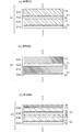
- FIG. 6 is a cross-sectional view schematically showing a part of an active layer provided in the semiconductor light emitting devices of Reference Examples 1 to 3.
- FIG. 4 is a graph comparing the light emission intensities of the semiconductor light emitting devices of Reference Examples 1 to 3.
- 6 is a table comparing applied voltages when current is injected at the same current density into the semiconductor light emitting devices of Reference Examples 1 to 3.
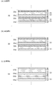
- FIG. 6 is a cross-sectional view schematically showing a part of an active layer included in the semiconductor light emitting devices of Examples 1 and 2 and Reference Example 4.
- 6 is a graph comparing the light emission intensities of the semiconductor light emitting devices of Examples 1 and 2 and Reference Example 4.
- 6 is a table comparing applied voltages when current is injected at the same current density into the semiconductor light emitting devices of Examples 1 and 2 and Reference Example 4. It is sectional drawing which shows typically the structure of the semiconductor light-emitting device of another embodiment. It is a graph which shows the relationship between the main light emission wavelength and internal quantum efficiency.
- the semiconductor light emitting device of the present invention will be described with reference to the drawings.
- the dimensional ratios in the drawings do not necessarily match the actual dimensional ratios.
- the numerical values related to the impurity concentration, the film thickness, the composition, and the number of periods related to the multilayer structure are merely examples, and are not limited to these numerical values.
- one direction is defined as “upper” and the other is defined as “lower” in the direction orthogonal to the main surface.
- This is a definition for convenience of explanation, and is inverted upside down. It is not intended to exclude the configuration. That is, in the description of the element, the description that “another layer B is formed above a certain layer A” includes a configuration in which the layer B is positioned above the layer A by inverting the element upside down. It is. Furthermore, this description includes the case where the layer B is formed on the upper surface of the layer A directly or via a thin film.
- FIG. 1 is a cross-sectional view schematically showing the structure of the semiconductor light emitting device of this embodiment.
- the semiconductor light emitting device 1 includes an n-type semiconductor layer 15, an active layer 30 formed on the n-type semiconductor layer, and a p-type semiconductor layer 43 formed on the active layer 30.
- the semiconductor light emitting device 1 has a substrate 11, an undoped GaN layer 13 is formed on the upper surface of the substrate 11, and an n-type semiconductor layer 15 is formed on the upper surface of the undoped GaN layer 13.
- the substrate 11 is composed of a sapphire substrate or a GaN substrate.
- the undoped GaN layer 13 is a layer formed by epitaxial growth on the c-plane of the substrate 11 and has a thickness of, for example, 3000 nm.
- the n-type semiconductor layer 15 is formed on the upper surface of the undoped GaN layer 13.
- the n-type semiconductor layer 15 is made of AlGaN having a film thickness of 2000 nm, an Si concentration as an n-type dopant of 3 ⁇ 10 19 / cm 3 , and an Al composition of 5%.
- the active layer 30 is made of a nitride semiconductor material so that the main emission wavelength is 520 nm or more.
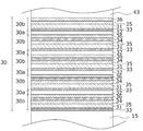
- FIG. 2 is a cross-sectional view schematically showing a part of the active layer 30 extracted.
- the active layer 30 is configured by repeating a laminated body of a light emitting layer 30a and a barrier layer 30b for a plurality of periods.
- the active layer 30 is described as a structure in which a stacked body of the light emitting layer 30a and the barrier layer 30b is repeated four periods, but is limited to this number of periods. As described above, it is not a thing.
- each light emitting layer 30a is disposed between the barrier layers 30b.
- the number of periods of the barrier layer 30b is one more than the number of periods of the light emitting layer 30a, but the content that “a stacked body of the light emitting layer 30a and the barrier layer 30b is repeated a plurality of periods” It is a concept that includes the structure. For example, by arranging the light emitting layer 30a arranged closest to the n-type semiconductor layer 15 on the upper surface of the n-type semiconductor layer 15, the number of periods of the light emitting layer 30a and the number of periods of the barrier layer 30b are completely set. You may match.
- Emitting layer 30a is formed of a second layer 32 consisting of In X2 Ga 1-X2 N ( 0.2 ⁇ X2 ⁇ 1).
- the second layer 32 is made of undoped InGaN having a film thickness of 2.6 nm and an In composition of 30%.
- the value of X 2 of In X2 Ga 1 -X2 N is appropriately selected according to the wavelength desired to be obtained as the main emission wavelength of the light emitted from the semiconductor light emitting device 1.
- the second layer 32 is made of InGaN having an In composition of 20% or more.
- the semiconductor light emitting device 1 having a main emission wavelength of 530 nm or more and 580 nm or less is realized by forming the second layer 32 of InGaN having an In composition of 25% or more and 35% or less.
- the film thickness of the second layer 32 is appropriately selected within a range in which a good film can be formed according to the value of the In composition of InGaN.
- the barrier layer 30b includes a first layer 31 made of undoped In X1 Ga 1 -X1 N (0 ⁇ X1 ⁇ 0.01), and undoped Al X3 Ga 1 -X3 N (0 ⁇ X3 ⁇ 1).
- a fifth layer 35 made of -X5-Y5 N (0 ⁇ X5 ⁇ 1, 0 ⁇ Y5 ⁇ 1) and a sixth layer 36 made of undoped In X6 Ga 1-X6 N (0 ⁇ X6 ⁇ 0.01) Is provided.
- each layer will be described.
- the barrier layer 30 b includes a third layer 33 on the side closest to the n-type semiconductor layer 15.
- the third layer 33 is made of undoped Al X3 Ga 1 -X3 N (0 ⁇ X3 ⁇ 1).
- the third layer 33 is made of undoped AlGaN having a thickness of 1.5 nm and an Al composition of 50%.
- the barrier layer 30 b includes the first layer 31 on the upper surface of the third layer 33.
- the first layer 31 is made of undoped In X1 Ga 1 -X1 N (0 ⁇ X1 ⁇ 0.01), that is, GaN or InGaN having a very low In composition.
- the first layer 31 is made of undoped GaN having a thickness of 9 nm.
- the barrier layer 30 b includes a fifth layer 35 on the upper surface of the first layer 31.
- the fifth layer 35 is composed of undoped Al x5 In Y5 Ga 1 -X5-Y5 N (0 ⁇ X5 ⁇ 1, 0 ⁇ Y5 ⁇ 1), preferably undoped AlGaN or undoped AlInGaN with a low In composition. Consists of.
- the fifth layer 35 is made of undoped AlGaN having a thickness of 5 nm and an Al composition of 5%.
- the barrier layer 30 b includes a fourth layer 34 on the upper surface of the fifth layer 35.
- the fourth layer 34 is composed of n-type Al x4 In Y4 Ga 1 -X4-Y4 N (0 ⁇ X4 ⁇ 1, 0 ⁇ Y4 ⁇ 1), preferably n-type AlGaN or undoped with a low In composition. Made of AlInGaN.
- the fourth layer 34 is made of n-type AlGaN having a thickness of 4 nm, an Al composition of 5%, and a Si concentration of 1 ⁇ 10 18 / cm 3 .
- the barrier layer 30b located on the side close to the p-type semiconductor layer 43 is more preferably configured not to include the fourth layer 34. The reason for this will be described later.
- the barrier layer 30 b includes a sixth layer 36 on the upper surface of the fourth layer 34.
- the sixth layer 36 is composed of undoped In X6 Ga 1 -X6 N (0 ⁇ X6 ⁇ 0.01), that is, GaN or InGaN having a very low In composition, like the first layer 31.
- the sixth layer 36 is made of undoped GaN having a thickness of 5 nm.
- the semiconductor light emitting device 1 includes a p-type semiconductor layer 43 on the upper surface of the active layer 30.
- the p-type semiconductor layer 43 is made of p-GaN having a thickness of 100 nm and a Mg concentration of 3 ⁇ 10 19 / cm 3 as a p-type dopant. If necessary, a high-concentration p-type contact layer can be provided on the p-GaN.
- the semiconductor light emitting device 1 of the present embodiment described with reference to FIGS. 1 and 2, a light emitting device having a main light emission wavelength of 520 nm or more capable of securing a high light emission intensity under a low driving voltage.
- the realization will be described with reference to an embodiment. Note that, as shown in an example described later (corresponding to Example 2), the semiconductor light emitting element 1 may be configured not to include the fifth layer 35 in the barrier layer 30b.
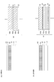
- FIG. 3 is a cross-sectional view schematically showing configurations of a conventional semiconductor light emitting device (Comparative Example 1) and a verification semiconductor light emitting device (Reference Example 1).
- symbol is attached
- the element of Comparative Example 1 is an active element formed by laminating a plurality of periods of a light emitting layer 60a composed of the second layer 32 composed of In X2 Ga 1 -X2 N and a barrier layer 60b composed of the undoped GaN layer 71. Layer 60 is included.
- the element of Reference Example 1 is composed of a light emitting layer 61a composed of the second layer 32 made of In X2 Ga 1 -X2 N, and undoped Al X3 Ga 1 -X3 N (0 ⁇ X3 ⁇ 1).
- the active layer 61 includes a third layer 33 formed and a barrier layer 61b formed of an undoped GaN layer 72 stacked in a plurality of periods.
- the element of Comparative Example 1 includes an electron block layer 57 made of p-AlGaN on the upper surface of the active layer 60, and a p-type semiconductor layer 43 made of p-GaN on the upper surface of the electron block layer 57. Is provided. This is provided for the purpose of preventing electrons injected from the n-type semiconductor layer 15 into the active layer 60 from entering the p-type semiconductor layer 43 beyond the active layer 60, and recombination in the active layer 60. There is an aim to suppress the decline in probability.
- the electron block layer 57 is made of AlGaN having a higher energy band gap than the active layer 60 and the p-type semiconductor layer 43 in order to form a barrier against electrons flowing from the active layer 60 to the p-type semiconductor layer 43.
- each element has a light emitting layer (60a, 61a) composed of InGaN having an In composition of 20% or more, for example, so that a main light emission wavelength is 520 nm or more. including.
- a light emitting layer 60a, 61a
- InGaN having such a high In composition it is necessary to make it lower than the general growth temperature of GaN, and this is the same even after the InGaN layer is formed. That is, when forming the electron blocking layer 57, it is necessary to grow AlGaN at a low temperature within a range in which the crystal of the light emitting layer 60a made of InGaN having a high In composition is not destroyed.
- Al is not sufficiently taken into GaN due to the parasitic reaction between the III group and the V group, pits are generated, and the film quality is deteriorated.
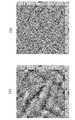
- FIG. 4 is a photograph comparing the surface states in the case where the electron blocking layer 57 is formed after the active layer 60 is formed in the element of Comparative Example 1 and in the case where the electron blocking layer 57 is not formed.
- FIG. 4A is a photograph of the surface state with the active layer 60 formed.
- FIG. 4B shows that after the active layer 60 is formed, it is made of AlGaN under a temperature condition (for example, about 880 ° C.) within a range not destroying the crystal state of the light emitting layer 60a made of InGaN having a high In composition.
- 4 is a photograph of a surface state on which a formed electron blocking layer 57 is formed. Both are photographs taken by AFM (Atomic Force Microscopy).
- FIG. 4B shows that the number of black dots on the surface is much larger than that in FIG. 4A. This black dot corresponds to the pit. That is, it can be seen from this photograph that an extremely large number of pits are formed when AlGaN is formed as the electron block layer 57. This suggests that a parasitic reaction has occurred by growing AlGaN at a low temperature as described above.
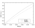
- FIG. 5 is a graph comparing the current-light output characteristics (IL characteristics) of the semiconductor light emitting device of Comparative Example 1 and the semiconductor light emitting device of Reference Example 1. According to FIG. 5, it is confirmed that the optical output of the element of Reference Example 1 is higher than that of the element of Comparative Example 1 under the condition where the same current is supplied.
- IL characteristics current-light output characteristics
- the semiconductor light emitting device of Comparative Example 1 since many pits (defects) are formed in the electron block layer 57, it is assumed that the pits become non-light emission centers and the light emission efficiency is lowered. Is done.
- the semiconductor light emitting device of Reference Example 1 achieves higher light output than the semiconductor light emitting device of Comparative Example 1. This is because the active layer 61 included in the semiconductor light emitting device of Reference Example 1 includes the third layer 33 made of AlGaN, so that the overflow of electrons is suppressed without providing the electron blocking layer 57. It is a suggestion. This is considered to be due to the following reasons.
- AlGaN constituting the third layer 33 has a hexagonal wurtzite structure and a mixed crystal, it lacks reversal symmetry in the c-axis direction and generates an electric field along the c-axis direction (spontaneous) polarization).
- the electric field derived from AlGaN is generated in a direction that cancels the piezoelectric field derived from InGaN. That is, since the active layer 61 includes the third layer 33 made of AlGaN, a piezoelectric field generated with respect to the active layer 61 is reduced.
- the bending of the band of an active layer can be made smaller than before.
- the decrease in the recombination probability of electrons and holes in the active layer is alleviated as compared with the conventional case, and the internal quantum efficiency is improved.
- the band gap energy of GaN is about 3.4 eV
- the band gap energy of InN is about 0.7 eV
- the band gap energy of AlN is about 6.2 eV.
- the undoped GaN layer 72 and the third layer 33 made of AlGaN constitute the barrier layer 61b
- the second layer 32 made of InGaN constitutes the light emitting layer 61a.
- the third layer 33 has an energy band gap higher than that of the undoped GaN layer 72, and functions as a layer for realizing a function of preventing the movement of electrons.
- the third layer 33 not only has a function of relaxing the piezoelectric field of InGaN as described above, but also overflows electrons from the n-type semiconductor layer 15 over the active layer 61 into the p-type semiconductor layer 43. It also has a function to suppress this. As a result, even if the electron blocking layer 57 is not separately provided as in the device of Comparative Example 1, the decrease in the recombination probability of electrons and holes due to the overflow of electrons is alleviated.
- the light emitting layer 61a is formed of the second layer 32 made of InGaN with a high In composition, the InGaN crystal is not broken in the subsequent growth process, and the semiconductor having a peak emission wavelength of 520 nm or more with high emission efficiency.
- a light emitting element can be realized.
- the semiconductor light emitting device 1 shown in FIGS. 1 and 2 has a configuration in which the active layer 30 includes the third layer 33 from such a viewpoint.
- each element of Reference Examples 1 to 4 and Examples 1 and 2 used in the following verification is configured to include the third layer 33.
- the semiconductor light emitting device 1 can realize a reduction in driving voltage and an improvement in light output using the devices of Reference Examples 1 to 4 including Reference Example 1 and the devices of Examples 1 and 2.
- FIG. 6 is a cross-sectional view schematically showing a part of the active layer included in the semiconductor light emitting devices of Reference Examples 1 to 3.
- the configuration of the active layer included in each element will be described.
- the element of Reference Example 2 includes a light emitting layer 62a composed of a second layer 32 made of In X2 Ga 1 -X2 N, and a third layer made of undoped Al X3 Ga 1 -X3 N (0 ⁇ X3 ⁇ 1). 33 and an active layer 62 in which a barrier layer 62b composed of a GaN layer 73 doped with n-type impurities is laminated in a plurality of periods. That is, as compared with the element of Reference Example 1, only the point that the GaN layer provided in the barrier layer is configured as an n-type is different.
- the light emitting layer 62a (second layer 32) is composed of InGaN with a film thickness of 2.6 nm and an In composition of 30%, and is made of undoped AlGaN with a film thickness of 1.5 nm and an Al composition of 50%.
- the barrier layer 62b was configured by the third layer 33 and the n-type GaN layer 73 having a film thickness of 23 nm and a Si concentration of 1 ⁇ 10 18 / cm 3 .
- the element of Reference Example 3 includes a light emitting layer 63a composed of a second layer 32 made of In X2 Ga 1 -X2 N, and a third layer made of undoped Al X3 Ga 1 -X3 N (0 ⁇ X3 ⁇ 1). 33, a first layer 31 made of undoped In X1 Ga 1 -X1 N (0 ⁇ X1 ⁇ 0.01), a GaN layer 73 doped with an n-type impurity, and undoped In X6 Ga 1 -X6 N (0 And an active layer 63 formed by laminating a plurality of periods with a barrier layer 63b composed of a sixth layer 36 composed of ⁇ X6 ⁇ 0.01).
- both the first layer 31 and the sixth layer 36 are composed of undoped GaN layers. That is, the element of Reference Example 3 is different from the element of Reference Example 2 in that the n-type GaN layer 73 is sandwiched between undoped GaN layers (31, 36).
- Al X3 Ga 1 -X 3 N and In X 6 Ga 1 -X 6 N are both assumed to be undoped InGaN with a low In composition, and have substantially the same functions as undoped GaN.
- FIG. 7A is a graph comparing the emission intensity for each wavelength when current is injected into each element of Reference Examples 1 to 3 at a current density of 25 A / cm 2 .
- FIG. 7B is a table showing applied voltages when current is injected into each element of Reference Examples 1 to 3 at a current density of 25 A / cm 2 .
- the device of the reference example 1 including the barrier layer 61b including the undoped GaN layer 72 includes the barrier layer (62b and 63b) including the n-type GaN layer 73.
- the emission intensity is higher than that of each of the three elements. This is considered to be caused by a phenomenon (droop phenomenon) in which the light emission efficiency is lowered by increasing the doping amount of Si.
- this droop phenomenon occurs is unknown at present, but as one consideration, the crystallinity of the GaN layer 73 included in each element of Reference Example 2 and Reference Example 3 deteriorated by doping Si into this GaN layer.
- the increase in the carrier density of the barrier layer resulted in an increase in Auger recombination, which is a non-luminescence factor, resulting in a decrease in the light output of each element of Reference Examples 2 and 3 compared to the element of Reference Example 1.
- the cause can be inferred.
- the device of Reference Example 3 is provided with a partially undoped GaN layer (31, 36), so that the thickness of the n-type GaN layer 73 is smaller than that of the device of Reference Example 2, and the amount of Si doped is small. It is less than the element of Reference Example 2. For this reason, it is presumed that the light emission intensity of the element of Reference Example 3 is located between the element of Reference Example 1 and the element of Reference Example 2.
- the emission intensity can be increased when the barrier layer is provided with an undoped GaN layer rather than the n-type GaN layer as in the element of Reference Example 1.
- the device of Reference Example 1 including the undoped GaN layer 72 in the barrier layer has a voltage required for injecting a current density of 25 A / cm 2 is 3.9 V. This is the highest compared to the devices of Reference Example 2 and Reference Example 3. Since the band of the barrier layer can be screened (the band structure is flattened) when the semiconductor layer is doped with impurities rather than when the semiconductor layer is undoped, the devices of Reference Example 2 and Reference Example 3 are the reference examples. The applied voltage can be made lower than that of the first element.
- FIG. 8 is a cross-sectional view schematically showing a part of the active layer included in each of the semiconductor light emitting devices of Examples 1 and 2 and Reference Example 4 described later.
- the element of Example 1 is the same as the semiconductor light emitting element 1 described above with reference to FIGS. 1 and 2. That is, in the element of Example 1, the light emitting layer 30a is composed of the second layer 32 made of In X2 Ga 1 -X2 N (0.2 ⁇ X2 ⁇ 1). Further, the barrier layer 30b is made of a third layer 33 made of undoped Al X3 Ga 1 -X3 N (0 ⁇ X3 ⁇ 1), and undoped In X1 Ga 1 -X1 N (0 ⁇ X1 ⁇ 0.01).
- the second layer 32 constituting the light emitting layer 30a was made of InGaN with a film thickness of 2.6 nm and an In composition of 30%.
- the third layer 33 is made of undoped AlGaN having a film thickness of 1.5 nm and an Al composition of 50%
- the first layer 31 is made of undoped GaN having a film thickness of 9 nm
- the fifth layer 35 is made of undoped AlGaN with a film thickness of 5 nm and an Al composition of 5%
- the fourth layer 34 is made of n-type AlGaN with an Al composition of 5%, a film thickness of 4 nm and an Si concentration of 1 ⁇ 10 18 / cm 3
- the sixth layer 36 was composed of undoped GaN having a thickness of 5 nm.
- the element of Example 2 is different from the element of Example 1 in that the fifth layer 35 is not provided. That is, in the device of Example 2, the light emitting layer 30a is configured by the second layer 32 made of In X2 Ga 1 -X2N , and the barrier layer 30b is the third layer made of undoped Al X3 Ga 1 -X3N. 33, a first layer 31 made of undoped In X1 Ga 1 -X1 N, a fourth layer 34 made of n-type Al x4 In Y4 Ga 1 -X4-Y4 N, and an undoped In X6 Ga 1 -X6 N The sixth layer 36 is formed.
- the second layer 32 constituting the light emitting layer 30a was made of InGaN with a film thickness of 2.6 nm and an In composition of 30%.
- the third layer 33 is made of undoped AlGaN having a film thickness of 1.5 nm and an Al composition of 50%
- the first layer 31 is made of undoped GaN having a film thickness of 9 nm
- the four layers 34 are made of n-type AlGaN having an Al composition of 5%, a film thickness of 9 nm, and a Si concentration of 1 ⁇ 10 18 / cm 3
- the sixth layer 36 is made of undoped GaN having a film thickness of 5 nm.
- the element of Reference Example 4 differs from the element of Example 2 in that an undoped AlGaN layer 74 is provided instead of the fourth layer 34 composed of n-type AlGaN. About the other point, it was made the same as the element of Example 2 including the thickness of each layer. That is, in the element of Reference Example 4, the light emitting layer 64a is composed of the second layer 32 made of InGaN with a film thickness of 2.6 nm and an In composition of 30%, and the barrier layer 64b has a film thickness of 1.5 nm and an Al composition of 50.
- Third layer 33 made of undoped AlGaN, first layer 31 made of 9 nm thick undoped GaN, Al composition 5%, 9 nm thick undoped AlGaN layer 74, and sixth layer made of 5 nm thick undoped GaN. 36.
- the thicknesses of the respective layers of Reference Examples 1 to 4 and Examples 1 and 2 are adjusted so that the thickness of one cycle of the active layer (30, 61, 62, 63, 64) is substantially equal. Has been.
- the element of Example 2 is different in that an n-type AlGaN layer (fourth layer 34) is provided instead of the n-type GaN layer 73 included in the barrier layer (63b) of the element of Reference Example 3. Further, the device of Example 2 is different in that an n-type AlGaN layer (fourth layer 34) is provided instead of the undoped AlGaN layer 74 included in the barrier layer (64b) of the device of Reference Example 4.
- the element of Example 1 includes an undoped AlGaN layer (fifth layer 35) between the n-type AlGaN layer (fourth layer 34) and the undoped GaN layer (first layer 31) in the element of Example 2. The point is different.
- FIG. 9A is a graph comparing the emission intensity for each wavelength when current is injected into each element of Examples 1 and 2 and Reference Example 4 at a current density of 25 A / cm 2 , as in FIG. 7A.
- FIG. 9B is a table showing applied voltages when current is injected into each element of Examples 1 and 2 and Reference Example 4 at a current density of 25 A / cm 2 .
- each of the elements of Example 1 and Example 2 exhibits higher emission intensity than any of the elements of Reference Examples 1 to 4.
- the element of Reference Example 4 also showed higher emission intensity than the elements of Reference Examples 1 to 3.
- the devices of Examples 1 and 2 and Reference Example 4 were compared with the devices of Reference Examples 1 to 3 by providing an AlGaN layer in the barrier layer as compared to the devices of Reference Examples 1 to 3. It is speculated that the improvement in crystallinity of the light emitting layer may be one of the reasons for improving the light output.
- the voltage required to inject a current density of 25 A / cm 2 into the element of Reference Example 4 is 4 V, which is the element of Reference Example 2 and Reference Example 3 Higher than that. This is considered to be due to the fact that the semiconductor layer was undoped as in the case where the required voltage was high in the element of Reference Example 1.
- the devices of Example 1 and Example 2 in which the barrier layer 30b includes the fourth layer 34 made of an n-type AlGaN layer are 25 A / cm 2 in the same manner as the devices of Reference Example 2 and Reference Example 3.
- the voltage required to inject the current density is suppressed to about 3.3 to 3.4V.
- Example 2 it can be seen that a light-emitting element with high emission intensity can be realized while keeping the driving voltage low. It is presumed that by providing the barrier layer 30b with an n-type AlGaN layer, electrons could be injected into the light emitting layer 30a with high efficiency while suppressing the droop phenomenon.
- the first layer made of n-type AlGaN was grown.
- Four layers 34 need to be grown. That is, after the film formation of the first layer 31 is completed, an Al source gas (for example, TMI (trimethylaluminum) or the like) and a source gas to be an n-type dopant (for example, tetraethylsilane or the like) are used to grow the fourth layer 34. ) Supply needs to be started additionally.
- a nitride semiconductor layer by MOCVD, if the growth conditions for growing successive layers are greatly different, the crystallinity of the layer may deteriorate due to abrupt changes in the growth conditions.
- the fifth layer 35 made of undoped AlGaN is grown, and then the fourth layer 34 made of n-type AlGaN is grown.
- the fifth layer 35 may be grown by additionally starting only the supply of the Al source gas, and further the film formation of the fifth layer 35 is performed.
- the third layer 33 may be grown by additionally starting only the supply of the source gas that becomes the n-type dopant. That is, since the change in growth conditions when growing the fourth layer 34 can be reduced as compared with the element of Example 2, the fourth layer 34 can be grown while maintaining good crystallinity. For this reason, it is surmised that the device of Example 1 shows higher light emission intensity than the device of Example 2.
- the barrier layer 30b (corresponding to the last barrier) positioned closest to the p-type semiconductor layer 43 is at least. More preferably, the fourth layer 34 made of n-type AlGaN is not provided. This is because electrons and holes are recombined at a position closer to the p-type semiconductor layer 43 than the light-emitting layer 30 a disposed closest to the p-type semiconductor layer 43, so that the light-emitting layer 30 a is changed from the p-type semiconductor layer 43. This is so as not to hinder the movement of holes toward the head.
- the last barrier includes the fourth layer 34, an effect of achieving both a reduction in driving voltage and an improvement in emission intensity can be obtained as compared with the elements of Reference Examples 1 to 3.
- All the barrier layers 30b other than the last barrier may be provided with the fourth layer 34, or a part of the barrier layers 30b other than the last barrier may be provided with the fourth layer 34.
- the barrier layers 30b at least one of the barrier layers 30b includes the fourth layer 34, so that it is possible to achieve both a reduction in driving voltage and an improvement in emission intensity as compared with the elements of Reference Examples 1 to 4. can get.
- Step S1 An undoped GaN layer 13 is grown on the upper layer of the substrate 11.
- An example of a specific method is as follows.
- a c-plane sapphire substrate is prepared as the substrate 11 and cleaned. More specifically, for this cleaning, for example, a substrate 11 (c-plane sapphire substrate) is disposed in a processing furnace of a MOCVD (Metal Organic Chemical Vapor Deposition) apparatus, and the flow rate is set in the processing furnace. While flowing 10 slm hydrogen gas, the furnace temperature is raised to, for example, 1150 ° C.
- MOCVD Metal Organic Chemical Vapor Deposition
- an undoped GaN layer 13 is formed by forming a low-temperature buffer layer made of GaN on the surface of the substrate 11 and further forming a base layer made of GaN thereon.
- a more specific method for forming the undoped GaN layer 13 is as follows.
- the furnace pressure of the ⁇ CVD apparatus is set to 100 kPa, and the furnace temperature is set to 480 ° C. Then, while flowing nitrogen gas and hydrogen gas with a flow rate of 5 slm respectively as carrier gas into the processing furnace, trimethylgallium (TMG) with a flow rate of 50 ⁇ mol / min and ammonia with a flow rate of 250,000 ⁇ mol / min are used as the raw material gas in the processing furnace. For 68 seconds. As a result, a low-temperature buffer layer made of GaN having a thickness of 20 nm is formed on the surface of the substrate 11.
- TMG trimethylgallium
- the furnace temperature of the MOCVD apparatus is raised to 1150 ° C. Then, while flowing nitrogen gas having a flow rate of 20 slm and hydrogen gas having a flow rate of 15 slm as a carrier gas in the processing furnace, TMG having a flow rate of 100 ⁇ mol / min and ammonia having a flow rate of 250,000 ⁇ mol / min are introduced into the processing furnace as source gases. Feed for 60 minutes. As a result, a base layer made of GaN having a thickness of 3 ⁇ m is formed on the surface of the low-temperature buffer layer. An undoped GaN layer 13 is formed by the low-temperature buffer layer and the base layer.
- a GaN substrate can be used as the substrate 11.
- the furnace temperature of the MOCVD apparatus is set to 1050 ° C.
- the nitrogen gas having a flow rate of 20 slm as the carrier gas and the flow rate of 15 slm in the processing furnace.
- TMG having a flow rate of 100 ⁇ mol / min and ammonia having a flow rate of 250,000 ⁇ mol / min are supplied into the processing furnace for 60 minutes.
- an undoped GaN layer 13 having a thickness of 3 ⁇ m is formed on the surface of the GaN substrate.
- Step S2 the n-type semiconductor layer 15 is formed on the upper surface of the undoped GaN layer 13.
- An example of a specific method is as follows.
- the furnace pressure of the MOCVD apparatus is set to 30 kPa in a state where the furnace temperature is 1150 ° C. Then, while flowing nitrogen gas having a flow rate of 20 slm and hydrogen gas having a flow rate of 15 slm as a carrier gas into the processing furnace, TMG having a flow rate of 94 ⁇ mol / min, trimethylaluminum (TMA) having a flow rate of 6 ⁇ mol / min, Ammonia having a flow rate of 250,000 ⁇ mol / min and tetraethylsilane having a flow rate of 0.025 ⁇ mol / min for doping n-type impurities are supplied into the processing furnace for 60 minutes.
- TMG trimethylaluminum
- Ammonia having a flow rate of 250,000 ⁇ mol / min
- tetraethylsilane having a flow rate of 0.025 ⁇ mol / min for doping n-type impurities are supplied into the processing furnace for 60
- an n-type semiconductor layer 15 made of AlGaN having an Al composition of 5%, having a Si concentration of 3 ⁇ 10 19 / cm 3 and a thickness of 2 ⁇ m is formed on the upper surface of the upper layer of the undoped GaN layer 13.
- the active layer 30 is formed on the upper surface of the n-type semiconductor layer 15.
- the active layer 30 of the present embodiment includes the light emitting layer 30a formed of the second layer 32 made of In X2 Ga 1 -X2 N (0.2 ⁇ X2 ⁇ 1), and the undoped Al X3 Ga.
- the barrier layer 30b includes a fourth layer 34 made of ⁇ 1) and a sixth layer 36 made of undoped In X6 Ga 1 -X6 N (0 ⁇ X6 ⁇ 0.01).
- step S3 is realized by executing the step of growing each of the semiconductor layers (31 to 36) a plurality of times.
- the furnace pressure of the MOCVD apparatus is 100 kPa
- the furnace temperature is 700 ° C. to 830 ° C.
- the flow rate is 15 slm nitrogen gas
- the flow rate is 1 slm hydrogen gas
- the flow rate is 375000 ⁇ mol / min.
- Ammonia may be continuously supplied into the processing furnace.
- Step S3a Under the condition where the furnace temperature is 690 ° C. and hydrogen gas, nitrogen gas, and ammonia are continuously supplied at the above flow rates, the flow rate is 27.2 ⁇ mol / min trimethylindium (TMI), and the flow rate is 15.2 ⁇ mol / min. Supply TMG for 54 seconds. As a result, a second layer 32 having a film thickness of 2.6 nm made of undoped InGaN having an In composition of 30% is formed.
- TMI trimethylindium
- step S3a it is preferable to set the growth rate to about 3 nm / min from the viewpoint of suppressing droplets as much as possible and promoting migration.
- Step S3b With the furnace temperature set at 690 ° C., hydrogen gas, nitrogen gas, and ammonia were continuously supplied at the above flow rates, and TMG with a flow rate of 15.2 ⁇ mol / min and TMA with a flow rate of 17.3 ⁇ mol / min were applied for 30 seconds. Supply continuously. As a result, the third layer 33 having a thickness of 1.5 nm and made of undoped AlGaN having an Al composition of 45% is formed.
- Step S3c The furnace temperature was set to 830 ° C., and TMG with a flow rate of 15.2 ⁇ mol / min was continuously supplied for 260 seconds under the state where hydrogen gas, nitrogen gas, and ammonia were continuously supplied at the above-described flow rates, A first layer 31 composed of undoped GaN is formed.
- a TMI having a flow rate of 1 ⁇ mol / min is additionally supplied to thereby form a first layer made of undoped InGaN having a thickness of 1 nm and an In composition of 1%.
- One layer 31 is formed. It is possible to form the first layer 31 in the process of raising the temperature after the end of step S3b.
- Step S3d With the furnace temperature set at 830 ° C., hydrogen gas, nitrogen gas, and ammonia were continuously supplied at the above flow rates, and TMG with a flow rate of 15.2 ⁇ mol / min and TMA with a flow rate of 0.8 ⁇ mol / min were applied for 120 seconds. Supply continuously. Thereby, the 5 nm-thick fifth layer 35 made of undoped AlGaN having an Al composition of 5% is formed. When the fifth layer 35 is made of AlInGaN having a low In composition, a low flow rate TMI may be additionally supplied.
- Step S3e With the furnace temperature set at 830 ° C., hydrogen gas, nitrogen gas, and ammonia were continuously supplied at the above-mentioned flow rates, TMG with a flow rate of 15.2 ⁇ mol / min, TMA with a flow rate of 0.8 ⁇ mol / min, and n Tetraethylsilane having a flow rate of 0.003 ⁇ mol / min for doping the type impurities is continuously supplied for 96 seconds. Thereby, a 4 nm-thick fourth layer 34 made of n-type AlGaN having an Al composition of 5% and an Si concentration of 1 ⁇ 10 18 / cm 3 is formed.
- the concentration of the n-type impurity in the fourth layer 34 can be, for example, 1 ⁇ 10 17 / cm 3 or more and 3 ⁇ 10 18 / cm 3 or less. Further, when the fourth layer 34 is made of AlInGaN having a low In composition, a low flow rate TMI may be additionally supplied.
- Step S3f With the furnace temperature set at 830 ° C., TMG having a flow rate of 15.2 ⁇ mol / min was continuously supplied for 130 seconds under the condition where hydrogen gas, nitrogen gas, and ammonia were continuously supplied at the above-described flow rates. A GaN layer is formed. As a result, a sixth layer 36 made of undoped GaN having a thickness of 5 nm is formed.
- the active layer 30 in which the light emitting layer 30a and the barrier layer 30b are stacked in a plurality of cycles is formed by repeatedly executing the above steps S3a to S3f a plurality of times.
- the semiconductor light emitting element 1 is more preferably configured not to grow the fourth layer 34 at least in the final period of the active layer 30.
- step S4d in the final cycle is not executed, and the thicknesses of layers other than the fourth layer 34 constituting the barrier layer 30b are appropriately adjusted so as to be substantially equal to the barrier layer 30b in other cycles. It doesn't matter.
- step S3d is not performed, but steps S3a to S3c and steps S3e to What is necessary is just to perform each process of S3f in multiple times.
- the thickness of the entire barrier layer 30b may be adjusted to about 25 nm by forming the fourth layer 34 so as to have a thickness of about 9 nm because the fifth layer 35 is not provided.
- Step S4 A p-type semiconductor layer 43 is formed on the upper surface of the active layer 30.
- An example of a specific method is as follows.
- the furnace pressure of the MOCVD apparatus is maintained at 100 kPa, and the furnace temperature is raised to 930 ° C. while nitrogen gas having a flow rate of 15 slm and hydrogen gas having a flow rate of 25 slm are allowed to flow into the processing furnace. Thereafter, as source gas, TMG having a flow rate of 100 ⁇ mol / min, ammonia having a flow rate of 250,000 ⁇ mol / min, and biscyclopentadienyl magnesium (Cp 2 Mg) having a flow rate of 0.1 ⁇ mol / min for doping p-type impurities. ) Is fed into the processing furnace for 360 seconds.
- a p-type semiconductor layer 43 made of GaN having a thickness of 120 nm and a p-type impurity (Mg) concentration of about 3 ⁇ 10 19 / cm 3 is formed on the upper surface of the active layer 30.
- a contact layer made of a high-concentration p-type GaN layer having a thickness of 5 nm may be formed by continuously changing the flow rate of Cp 2 Mg to 0.3 ⁇ mol / min and supplying a source gas for 20 seconds.
- the contact layer is also included in the p-type semiconductor layer 43.
- the contact layer has a p-type impurity (Mg) concentration of about 1 ⁇ 10 20 / cm 3 .
- the said embodiment demonstrated the case where the p-type impurity contained in the p-type semiconductor layer 43 was Mg, Be, Zn, and C other than Mg can be used.
- the lateral structure semiconductor light emitting device 1 a part of the upper surface of the n-type semiconductor layer 15 is exposed by ICP etching, an n-side electrode is formed on the exposed upper layer of the n-type semiconductor layer 15, and a p-type semiconductor layer is formed. A p-side electrode is formed on the upper layer 43. And each element is isolate
- the “lateral structure” means that the n-side electrode formed in the upper layer of the n-type semiconductor layer 15 and the p-side electrode formed in the upper layer of the p-type semiconductor layer 43 are parallel to the surface of the substrate. Refers to a structure arranged in various directions.
- a metal electrode (reflection electrode) serving as a p-side electrode, a solder diffusion preventing layer, and a solder layer are formed on the p-type semiconductor layer 43.
- the support substrate for example, CuW board
- substrate 11 is peeled by methods, such as a laser irradiation, upside down.
- an n-side electrode is formed on the n-type semiconductor layer 15.
- element isolation and wire bonding are performed as in the horizontal structure.
- the “vertical structure” refers to a structure in which an n-side electrode and a p-side electrode are arranged in a direction orthogonal to the surface of the substrate.
- the third layer 33 made of undoped Al X3 Ga 1 -X3 N (0 ⁇ X3 ⁇ 1) may not be provided in all periods of the barrier layer 30b.
- the barrier layer 30 b includes the third layer 33 only at a position close to the p-type semiconductor layer 43 and does not include the third layer 33 at a position close to the n-type semiconductor layer 15. . This is due to the following reason.
- the third layer 33 made of AlGaN has an energy band gap larger than that of the first layer 31 made of GaN (or InGaN having a low In composition)
- electrons are on the p-type semiconductor layer 43 side. It constitutes an energy barrier when moving to.
- the barrier layer 30b closest to the n-type semiconductor layer 15 includes the third layer 33 made of AlGaN
- an energy barrier is also formed by the third layer 33 in the vicinity of the n-type semiconductor layer 15. End up.
- the electrons supplied from the n-type semiconductor layer 15 are blocked from moving by this energy barrier formed at a position close to the n-type semiconductor layer 15 and are formed by the second layer 32 (light emitting layer 30a). There is a possibility that the probability that electrons are taken into the region is lowered.
- the barrier layer 30b close to the n-type semiconductor layer 15 is configured not to include the third layer 33, so that a high energy barrier that blocks the movement of electrons is generated in the region formed on the n-type semiconductor layer 15 side. not exist. Therefore, when a voltage is applied to the semiconductor light emitting device 1, electrons flow into the active layer 30 with a high probability up to the place where the third layer 33 is formed. Then, movement of some electrons is blocked by the energy barrier of the third layer 33, so that electrons can be taken into the well region formed by the second layer 32 with high probability. As a result, electrons and holes can be recombined with high probability in the well region.
- the barrier layer 30b period of comprising a fourth layer 34 of n-type Al x4 In Y4 Ga 1-X4 -Y4 N (0 ⁇ X4 ⁇ 1,0 ⁇ Y4 ⁇ 1), the first layer 31 And the third layer 33 may be provided.
- the semiconductor light emitting element 1 may further include a relaxation layer 20 between the n-type semiconductor layer 15 and the active layer 30.
- the relaxation layer 20 can be composed of a single layer of AlInGaN or a superlattice layer of GaN / (Al) InGaN.
- the GaN layer and the InGaN layer are both formed by laminating 10 periods with a film thickness of 2.5 nm.
- the In composition of the InGaN layer is 7%, and both the GaN layer and the InGaN layer are doped with Si concentration of 1 ⁇ 10 18 / cm 3 to be n-type.
- the crystal is intended when the active layer 30 is grown.
- the effect of reducing the lattice strain on the active layer 30 including the second layer 32 made of InGaN having a high In composition and further improving the light emission efficiency is expected.
- Step S2A may be executed.
- Step S2A When the relaxation layer 20 is composed of a superlattice layer, it can be manufactured by the following method. First, the furnace pressure of the MOCVD apparatus is 100 kPa, and the furnace temperature is 820 ° C. Then, while flowing nitrogen gas having a flow rate of 15 slm and hydrogen gas having a flow rate of 1 slm as a carrier gas into the processing furnace, TMG having a flow rate of 15.2 ⁇ mol / min, TMI having a flow rate of 27.2 ⁇ mol / min, A step of supplying tetraethylsilane having a flow rate of 0.003 ⁇ mol / min and ammonia having a flow rate of 375000 ⁇ mol / min into the processing furnace for 54 seconds is performed.
- a step of supplying TMG having a flow rate of 15.2 ⁇ mol / min and ammonia having a flow rate of 375000 ⁇ mol / min into the processing furnace for 54 seconds is performed.
- an InGaN layer having a Si concentration of 1 ⁇ 10 18 / cm 3 , a thickness of 2.5 nm and an In composition of 7% and a GaN layer having a thickness of 2.5 nm are stacked in 10 cycles.
- a relaxation layer 20 is formed on the upper surface of the n-type semiconductor layer 15.
- the relaxation layer 20 can also be configured as a stacked body of InGaN having a low In composition and InGaN having a high In composition.
- this step S2A while flowing nitrogen gas having a flow rate of 15 slm and hydrogen gas having a flow rate of 1 slm, TMG having a flow rate of 15.2 ⁇ mol / min, TMI having a flow rate of 27.2 ⁇ mol / min, A step of supplying tetraethylsilane having a flow rate of 0.003 ⁇ mol / min and ammonia having a flow rate of 375,000 ⁇ mol / min into the processing furnace for 54 seconds, TMG having a flow rate of 15.2 ⁇ mol / min, TMI having a flow rate of 1 ⁇ mol / min, and a flow rate of A step of supplying 375,000 ⁇ mol / min of ammonia into the processing furnace for 54 seconds is performed.
- a relaxation layer 20 formed by laminating 10 layers is formed on the upper surface of the n-type semiconductor layer 15.
- the relaxation layer 20 is composed of a single film of AlInGaN, it can be manufactured by the following method.
- the furnace pressure of the MOCVD apparatus is 100 kPa, and the furnace temperature is 820 ° C.
- TMG having a flow rate of 15.2 ⁇ mol / min
- TMI having a flow rate of 27.2 ⁇ mol / min
- a step of supplying TMA having a flow rate of 1 ⁇ mol / min, tetraethylsilane having a flow rate of 0.003 ⁇ mol / min, and ammonia having a flow rate of 375000 ⁇ mol / min into the processing furnace for 400 seconds is performed.
- a relaxation layer 20 composed of an AlInGaN layer having an Si concentration of 1 ⁇ 10 18 / cm 3 , a thickness of 20 nm and an Al composition of 6% and an In composition of 7% is formed on the upper surface of the n-type semiconductor layer 15.
- SYMBOLS 1 Semiconductor light emitting element 11: Substrate 13: Undoped GaN layer 15: N-type semiconductor layer 20: Relaxation layer 30: Active layer 30a: Light emitting layer 30b: Barrier layer 31: First layer (Undoped In X1 Ga 1-X1 N layer) 32: Second layer (undoped In X2 Ga 1 -X2 N layer) 33: Third layer (undoped Al X3 Ga 1-X3 N layer) 34: fourth layer (n-type Al x4 In Y4 Ga 1-X4 -Y4 N layer) 35: Fifth layer (undoped Al x5 In Y5 Ga 1 -X5-Y5 N layer) 36: Sixth layer (undoped In X6 Ga 1 -X6 N layer) 43: p-type semiconductor layer 57: electron block layer 60: active layer provided in the device of Comparative Example 1 60a: light emitting layer provided in the device of Comparative Example 1 60b: barrier layer provided in the device of Comparative Example
Landscapes
- Led Devices (AREA)
Abstract
低い駆動電圧の下で高い光出力の確保が可能な、主たる発光波長が520nm以上の窒化物半導体発光素子を提供する。 本発明は、主たる発光波長が520nm以上の半導体発光素子であって、n型半導体層とp型半導体層の間に活性層を備える構成である。この活性層は、アンドープのInX1Ga1-X1N(0≦X1≦0.01)からなる第一層を含む障壁層と、InX2Ga1-X2N(0.2≦X2<1)からなる第二層を含む発光層との積層体が複数周期繰り返されることで構成されている。障壁層は、少なくともいずれか一の周期内において、アンドープのAlX3Ga1-X3N(0<X3<1)からなる第三層と、第三層の上層に形成された第一層と、第一層の上層に形成されたn型のAlx4InY4Ga1-X4-Y4N(0<X4<1,0≦Y4<1)からなる第四層とを含む。
Description
本発明は半導体発光素子に関し、特に主たる発光波長が520nm以上を示す半導体発光素子に関する。
近年、可視光領域の発光波長を持つLEDを用いたプロジェクタや医療用検査装置の開発が進んでいる。可視光領域の発光波長を持つLEDとしては、従来GaP系の化合物半導体が主に用いられている。しかし、GaP系の化合物半導体は、バンド構造が間接遷移型の半導体であり、遷移確率が低いことから、発光効率の上昇は困難であった。そこで、直接遷移型の半導体である窒化物半導体系の材料を用いた、可視光領域のLEDの開発が進められている。
可視光領域の発光に関し、特に520nm以上の波長域は高効率化が難しく、発光効率が著しく低下することが知られている。図11は、主たる発光波長と内部量子効率の関係を示すグラフであり、横軸が主たる発光波長に対応し、縦軸が内部量子効率(IQE)に対応する。図11によれば、主たる発光波長が520nmを超えると内部量子効率が急激に低下していることが確認できる。このように内部量子効率が低下する波長領域は「グリーンギャップ領域」と呼ばれ、GaP系や窒化物半導体系に関わらず、かかる波長領域において効率が低下することが問題となっている。このため、このグリーンギャップ領域において、内部量子効率を高めて発光効率を高めることが要請されている。
特に520nm以上の波長域において発光効率が低下する理由の一つに、ピエゾ電界に起因した活性層内での電子と正孔の再結合確率の低下が挙げられる。この点につき、窒化物半導体を例に挙げて説明する。
GaNやAlGaNなどの窒化物半導体は、ウルツ鉱型結晶構造(六方晶構造)を有している。ウルツ鉱型結晶構造の面は、4指数表記(六方晶指数)にて、a1、a2、a3及びcで示される基本ベクトルを用いて結晶面や方位が表される。基本ベクトルcは、[0001]方向に延びており、この方向は「c軸」と呼ばれる。c軸に垂直な面は「c面」又は「(0001)面」と呼ばれる。
従来、窒化物半導体を用いて半導体発光素子を作製する場合、窒化物半導体結晶を成長させる基板として、c面基板を主面に有する基板が使用される。実際にはこの基板上に低温下でGaN層を成長させ、更にその上層に窒化物半導体層を成長させる。なお、発光に寄与する層を構成する活性層としては、GaNとInNの混晶であるInGaNが用いられるのが一般的である。
ここで、GaNとInNには格子定数に差が存在する。具体的には、a軸方向に関し、GaNの格子定数は0.3189nmである一方、InNの格子定数は0.354nmである。このため、GaN層より上層にGaNよりも格子定数の大きいInNを含むInGaN層を成長させると、InGaN層は成長面と垂直方向に圧縮歪みを受ける。このとき、正電荷を持つGa及びInと負電荷を持つNとの分極のバランスが崩れ、c軸方向に沿った電界が発生する(ピエゾ電界)。ピエゾ電界が活性層に発生すると、この活性層のバンドが曲がって電子と正孔の波動関数の重なり度合いが小さくなり、活性層内での電子と正孔の再結合確率が低下する(いわゆる「量子閉じ込めシュタルク効果」)。これにより、内部量子効率が低下する。
発光波長を520nm以上にするためには、当該波長に応じたバンドギャップエネルギーを実現するために活性層(特に発光層)に含まれるIn組成を高める必要がある。しかし、In組成を高めると圧縮歪みが大きくなるため、ピエゾ電界が大きくなる。この結果、内部量子効率が更に低下する。
内部量子効率を高める方法として、下記特許文献1では、非極性面、例えば[10-10]方向に垂直な、m面と呼ばれる(10-10)面を表面に有する基板を使用して活性層を成長させることで、活性層にピエゾ電界を生じさせないようにした発光素子が検討されている。
本発明者は、鋭意研究により、主たる発光波長が520nm以上の窒化物半導体からなる発光素子においては、駆動電圧が上昇してしまうという課題と、光出力が低下してしまうという課題が二律背反の状態にあることを突き止めた。
本発明は、低い駆動電圧の下で高い光出力の確保が可能な、主たる発光波長が520nm以上の窒化物半導体発光素子を提供することを目的とする。
本発明は、主たる発光波長が520nm以上の半導体発光素子であって、
窒化物半導体からなるn型半導体層と、
前記n型半導体層の上層に形成された、窒化物半導体からなる活性層と、
前記活性層の上層に形成された、窒化物半導体からなるp型半導体層とを備え、
前記活性層は、アンドープのInX1Ga1-X1N(0≦X1≦0.01)からなる第一層を含む障壁層と、InX2Ga1-X2N(0.2≦X2<1)からなる第二層を含む発光層との積層体が複数周期繰り返されることで構成されており、
前記障壁層は、少なくともいずれか一の周期内において、アンドープのAlX3Ga1-X3N(0<X3<1)からなる第三層と、前記第三層の上層に形成された前記第一層と、前記第一層の上層に形成されたn型のAlx4InY4Ga1-X4-Y4N(0<X4<1,0≦Y4<1)からなる第四層とを含むことを特徴とする。
窒化物半導体からなるn型半導体層と、
前記n型半導体層の上層に形成された、窒化物半導体からなる活性層と、
前記活性層の上層に形成された、窒化物半導体からなるp型半導体層とを備え、
前記活性層は、アンドープのInX1Ga1-X1N(0≦X1≦0.01)からなる第一層を含む障壁層と、InX2Ga1-X2N(0.2≦X2<1)からなる第二層を含む発光層との積層体が複数周期繰り返されることで構成されており、
前記障壁層は、少なくともいずれか一の周期内において、アンドープのAlX3Ga1-X3N(0<X3<1)からなる第三層と、前記第三層の上層に形成された前記第一層と、前記第一層の上層に形成されたn型のAlx4InY4Ga1-X4-Y4N(0<X4<1,0≦Y4<1)からなる第四層とを含むことを特徴とする。
上記の構成によれば、駆動電圧を低下しながらも高い光出力が確保できる、主たる発光波長が520nm以上の半導体発光素子が実現される。この内容については、「発明を実施するための形態」の項で後述される。第四層は、低In組成のn型のAlx4InY4Ga1-X4-Y4N(例えばY4≦0.01)、又はn型のAlGaNで構成することができる。
ところで、本明細書において、「AlGaN」という記述は、AlmGa1-mN(0<m<1)という記述と同義であり、AlとGaの組成比の記述を単に省略して記載したものであって、AlとGaの組成比が1:1である場合に限定する趣旨ではない。「InGaN」、「AlInGaN」等という記述についても同様である。
ここで、第四層は、全ての周期の障壁層に含まれていても構わないし、いずれか一又は複数の周期の障壁層に含まれていても構わない。ただし、p型半導体層に最も近い障壁層は第四層を含まない構成とするのがより好ましい。これは、p型半導体層に最も近い側に位置する発光層よりも更にp型半導体層に近い側において、電子と正孔が再結合することで、正孔の発光層側への移動の妨げにならないようにするためである。
上記の構成において、前記障壁層は、少なくともいずれか一の周期内において、前記第三層と、前記第三層の上層に形成された前記第一層と、前記第一層の上層に形成されたアンドープのAlx5InY5Ga1-X5-Y5N(0<X5<1,0≦Y5<1)からなる第五層と、前記第五層の上層に形成された前記第四層とを含むものとしても構わない。なお、第五層は、低In組成のアンドープのAlx5InY5Ga1-X5-Y5N(例えばY5≦0.01)、又はアンドープのAlGaNで構成することができる。
また、前記障壁層は、少なくともいずれか一の周期内において、前記第三層と、前記第三層の上層に形成された前記第一層と、前記第一層の上層に形成された前記第四層と、前記第四層の上層に形成されたアンドープのInX6Ga1-X6N(0≦X6≦0.01)からなる第六層を含み、
前記p型半導体層に最も近い周期を除く少なくともいずれか一の周期内の前記障壁層が含む前記第六層の上面に、前記発光層を構成する前記第二層が配置されているものとしても構わない。
前記p型半導体層に最も近い周期を除く少なくともいずれか一の周期内の前記障壁層が含む前記第六層の上面に、前記発光層を構成する前記第二層が配置されているものとしても構わない。
第六層は、低In組成のアンドープのInGaN又はアンドープのGaNで構成される。以下では第六層がアンドープのGaNで構成される場合について説明する。
主たる発光波長が520nm以上の半導体発光素子を実現すべく、高いIn組成(20%以上)のInGaNからなる第二層を形成する場合には、当該第二層の成長時に成長温度を低下させる必要がある。ここで、n型のAlx4InY4Ga1-X4-Y4N(0<X4<1,0≦Y4<1)からなる第四層を成長させた後に、発光層を構成するInGaN(第二層)を成長させるべく温度を低下させると、第二層を成長させるための温度に安定するまでの間に、Alx4InY4Ga1-X4-Y4NからGaが蒸発して第四層の組成が変化するおそれがある。これに対し、第四層の上層に、GaNからなる第六層を形成しておき、この状態でInGaNの成長温度まで低下させることで、第四層の組成を安定化させることができる。なお、この効果は、第六層が低In組成のInGaNで構成される場合においても同様に実現できる。
なお、前記第二層は、InX2Ga1-X2N(0.25≦X2≦0.35)で構成されるものとしても構わない。この場合、主たる発光波長が530nm以上580nm以下の半導体発光素子が実現される。
本発明によれば、低い駆動電圧の下で高い光出力の確保が可能な、主たる発光波長が520nm以上の窒化物半導体発光素子が実現される。
本発明の半導体発光素子につき、図面を参照して説明する。なお、以下の各図面において、図面の寸法比と実際の寸法比は必ずしも一致しない。また、以下の説明において、不純物濃度、膜厚、組成、及び多層構造体に係る周期数に関する数値はあくまで一例であり、これらの数値に限定されるものではない。
また、本明細書では、主面に直交する方向につき、一方を「上方」、他方を「下方」と規定して説明するが、これは説明の便宜上の定義であり、上下を反転させてなる構成を排除する趣旨ではない。すなわち、素子に関する説明において、「ある層Aの上層に別の層Bが形成される」という記載は、この素子の上下を反転させることで層Aの上層に層Bが位置する構成も含む趣旨である。更に、この記載は、層Aの上面に、直接又は薄膜を介して層Bが形成されている場合を含む趣旨である。
[構造]
図1は、本実施形態の半導体発光素子の構造を模式的に示す断面図である。半導体発光素子1は、n型半導体層15と、n型半導体層の上層に形成された活性層30と、活性層30の上層に形成されたp型半導体層43を備える。
図1は、本実施形態の半導体発光素子の構造を模式的に示す断面図である。半導体発光素子1は、n型半導体層15と、n型半導体層の上層に形成された活性層30と、活性層30の上層に形成されたp型半導体層43を備える。
より詳細には、半導体発光素子1は基板11を有し、基板11の上面にアンドープのGaN層13が形成され、アンドープのGaN層13の上面にn型半導体層15が形成されている。基板11はサファイア基板又はGaN基板で構成される。アンドープのGaN層13は、基板11のc面にエピタキシャル成長によって形成された層であり、例えば3000nmの膜厚で構成される。
n型半導体層15は、アンドープのGaN層13の上面に形成されている。本実施形態では、一例として、n型半導体層15は、膜厚が2000nm、n型ドーパントとしてのSi濃度が3×10¹⁹/cm3、Al組成が5%のAlGaNで構成される。
活性層30は、主たる発光波長が520nm以上となるよう、窒化物半導体材料で構成されている。図2は、活性層30の一部分を抜き出して模式的に示した断面図である。図2に示すように、活性層30は、発光層30aと障壁層30bとの積層体が複数周期繰り返されることで構成されている。一例として、本実施形態の半導体発光素子1は、活性層30が、発光層30a及び障壁層30bの積層体が4周期繰り返されて構成されるものとして説明するが、この周期数に限定されるものではないことは上述した通りである。
また、図2に示す例では、各発光層30aが障壁層30bに挟まれて配置されている場合を図示している。この場合、障壁層30bの周期数が、発光層30aの周期数よりも1だけ多くなるが、「発光層30aと障壁層30bとの積層体が複数周期繰り返される」という内容は、このような構成も含む概念である。なお、例えばn型半導体層15に最も近い位置に配置されている発光層30aをn型半導体層15の上面に配置することで、発光層30aの周期数と障壁層30bの周期数を完全に一致させても構わない。
発光層30aは、InX2Ga1-X2N(0.2≦X2<1)からなる第二層32によって構成される。一例として、第二層32は、膜厚2.6nmでIn組成30%のアンドープInGaNで構成される。
なお、InX2Ga1-X2NのX2の値、すなわちIn組成の値については、半導体発光素子1から発せられる光の主たる発光波長として得たい波長に応じて適宜選択される。本実施形態では、主たる発光波長が520nm以上の半導体発光素子1を想定しているため、第二層32はIn組成が20%以上であるInGaNで構成される。なお、In組成が25%以上35%以下であるInGaNで第二層32を構成することで、主たる発光波長が530nm以上580nm以下の半導体発光素子1が実現される。また、第二層32の膜厚は、InGaNのIn組成の値に応じて良好な成膜が可能な範囲内で適宜選択される。
本実施形態において、障壁層30bは、アンドープのInX1Ga1-X1N(0≦X1≦0.01)からなる第一層31、アンドープのAlX3Ga1-X3N(0<X3<1)からなる第三層33、n型のAlx4InY4Ga1-X4-Y4N(0<X4<1,0≦Y4<1)からなる第四層34、アンドープのAlx5InY5Ga1-X5-Y5N(0<X5<1,0≦Y5<1)からなる第五層35、及びアンドープのInX6Ga1-X6N(0≦X6≦0.01)からなる第六層36を備える。以下、各層について説明する。
障壁層30bは、n型半導体層15に最も近い側に第三層33を備えている。この第三層33は、アンドープのAlX3Ga1-X3N(0<X3<1)で構成され、一例として、膜厚1.5nmでAl組成50%のアンドープAlGaNで構成される。
障壁層30bは、第三層33の上面に第一層31を備えている。この第一層31は、アンドープのInX1Ga1-X1N(0≦X1≦0.01)、すなわちGaN又は極めてIn組成の低いInGaNで構成される。一例として、第一層31は膜厚9nmのアンドープGaNで構成される。
障壁層30bは、第一層31の上面に第五層35を備える。この第五層35は、アンドープのAlx5InY5Ga1-X5-Y5N(0<X5<1,0≦Y5<1)で構成され、好ましくはアンドープのAlGaN又はIn組成の低いアンドープのAlInGaNで構成される。一例として、第五層35は膜厚5nmでAl組成5%のアンドープAlGaNで構成される。
障壁層30bは、第五層35の上面に第四層34を備える。この第四層34は、n型のAlx4InY4Ga1-X4-Y4N(0<X4<1,0≦Y4<1)で構成され、好ましくはn型のAlGaN又はIn組成の低いアンドープのAlInGaNで構成される。一例として、第四層34は、膜厚4nm、Al組成5%、Si濃度が1×10¹⁸/cm3のn型AlGaNで構成される。
なお、各障壁層30bのうち、p型半導体層43に近い側に位置する障壁層30bは、この第四層34を備えない構成とするのがより好ましい。この理由については後述される。
障壁層30bは、第四層34の上面に第六層36を備える。第六層36は、アンドープのInX6Ga1-X6N(0≦X6≦0.01)、すなわち第一層31と同様に、GaN又は極めてIn組成の低いInGaNで構成される。一例として、第六層36は膜厚5nmのアンドープGaNで構成される。
また、半導体発光素子1は、活性層30の上面にp型半導体層43を備える。このp型半導体層43は、一例として膜厚が100nm、p型ドーパントとしてのMg濃度が3×10¹⁹/cm3のp-GaNで構成される。なお、必要に応じてこのp-GaNの上層に高濃度p型のコンタクト層を設けることができる。
以下、図1及び図2を参照して説明した本実施形態の半導体発光素子1によれば、低い駆動電圧の下で高い発光強度の確保が可能な、主たる発光波長が520nm以上の発光素子が実現される点について、実施例を参照しながら説明する。なお、後述の実施例(実施例2に対応する。)において示されるように、半導体発光素子1は障壁層30bに第五層35を備えない構成としても構わない。
[第三層33についての分析]
従来、窒化物半導体からなる主たる発光波長が520nm以上の半導体発光素子においては、InGaNからなる発光層とGaNからなる障壁層が複数周期積層されて構成される活性層を備えた素子が開発されていた。しかし、本発明者の鋭意研究により、障壁層をGaN/AlGaNで構成することで発光強度が従来よりも向上することを見出した。本発明は、この内容を前提としてなされたものである。この点につき、検証用の素子(参考例1~3)の発光強度を従来の素子と比較しながら説明する。
従来、窒化物半導体からなる主たる発光波長が520nm以上の半導体発光素子においては、InGaNからなる発光層とGaNからなる障壁層が複数周期積層されて構成される活性層を備えた素子が開発されていた。しかし、本発明者の鋭意研究により、障壁層をGaN/AlGaNで構成することで発光強度が従来よりも向上することを見出した。本発明は、この内容を前提としてなされたものである。この点につき、検証用の素子(参考例1~3)の発光強度を従来の素子と比較しながら説明する。
図3は、従来の半導体発光素子(比較例1)と、検証用の半導体発光素子(参考例1)の構成を模式的に示した断面図である。なお、図2と同一の箇所については同一の符号を付している。
比較例1の素子は、InX2Ga1-X2Nからなる第二層32で構成された発光層60aと、アンドープのGaN層71からなる障壁層60bとが複数周期積層されて構成される活性層60を含む。これに対し、参考例1の素子は、InX2Ga1-X2Nからなる第二層32で構成された発光層61aと、アンドープのAlX3Ga1-X3N(0<X3<1)からなる第三層33及びアンドープのGaN層72からなる障壁層61bとが複数周期積層されて構成される活性層61を含む。
また、比較例1の素子は、活性層60の上面に、p-AlGaNで構成された電子ブロック層57を備え、この電子ブロック層57の上面にp-GaNで構成されたp型半導体層43を備える。これは、n型半導体層15から活性層60へ注入される電子が当該活性層60を越えてp型半導体層43内に入るのを防止する目的で設けられており、活性層60における再結合確率の低下を抑制する狙いがある。電子ブロック層57は、活性層60からp形半導体層43へ流れる電子に対する障壁を構成すべく、活性層60やp型半導体層43よりもエネルギーバンドギャップの高いAlGaNで構成される。
上述したように、比較例1及び参考例1の双方において、各素子は、主たる発光波長が520nm以上となるよう、例えばIn組成が20%以上のInGaNで構成された発光層(60a,61a)を含む。このように高いIn組成のInGaNを成長させるに際しては、一般的なGaNの成長温度よりは低温にする必要があり、これは、InGaN層を形成した後においても同様である。つまり、電子ブロック層57を形成するに際しては、高いIn組成のInGaNからなる発光層60aの結晶が破壊されない範囲内の低温下でAlGaNを成長させる必要がある。しかし、これに伴い、III族とV族との寄生反応に起因してAlがGaNに十分に取り込まれず、ピットが発生して膜質が低下する。
図4は、比較例1の素子において活性層60を形成後、電子ブロック層57を形成した場合と電子ブロック層57を形成しない場合とでの表面状態を比較した写真である。図4(a)は、活性層60を形成した状態における表面状態の写真である。また、図4(b)は、活性層60を形成した後に、高いIn組成のInGaNからなる発光層60aの結晶状態を破壊しない範囲内の温度条件下(例えば880℃程度)で、AlGaNで構成された電子ブロック層57を形成した表面状態の写真である。いずれも、AFM(Atomic Force Microscopy:原子間力顕微鏡)によって撮影された写真である。
図4(b)の写真は、図4(a)の写真よりも表面に黒い点の数が極めて多いことが見て取れる。この黒い点はピットに対応する。つまり、この写真から、電子ブロック層57としてのAlGaNを形成した際に極めて多数のピットが形成されていることが分かる。これは、上述したように、AlGaNを低温で成長させたことで寄生反応が生じていることを示唆するものである。
図5は、比較例1の半導体発光素子と参考例1の半導体発光素子の電流光出力特性(I-L特性)を比較したグラフである。図5によれば、同一電流を供給した状態の下で、参考例1の素子の方が比較例1の素子よりも高い光出力が実現されていることが確認される。
上述したように、比較例1の半導体発光素子は、電子ブロック層57に多くのピット(欠陥)が形成されているため、このピットが非発光中心となり、発光効率が低下しているものと推察される。これに対し、参考例1の半導体発光素子は、比較例1の半導体発光素子よりも高い光出力が実現されている。これは、参考例1の半導体発光素子が備える活性層61が、AlGaNで構成された第三層33を備えることで、電子ブロック層57を設けなくても電子のオーバーフローが抑制されていることを示唆するものである。これは、以下の理由によるものと考えられる。
第三層33を構成するAlGaNは、結晶構造が六方晶ウルツ鉱構造であり、混晶であることからもc軸方向の反転対称性を欠き、c軸方向に沿った電界が発生する(自発分極)。AlGaNの自発分極による電界がInGaNとは反対方向に加わる結果、AlGaN由来の電界は、InGaN由来のピエゾ電界を打ち消す方向に発生する。つまり、活性層61が、AlGaNで構成された第三層33を有することで、活性層61に対して生じるピエゾ電界が緩和される。これにより、従来よりも活性層のバンドの曲がりを小さくすることができる。この結果、活性層における電子と正孔の再結合確率の低下が従来よりも緩和され、内部量子効率が向上する。
また、一般に、GaNのバンドギャップエネルギーが約3.4eV、InNのバンドギャップエネルギーが約0.7eV、AlNのバンドギャップエネルギーが約6.2eVである。このため、参考例1の素子が備える活性層61において、アンドープのGaN層72及びAlGaNからなる第三層33が障壁層61bを構成し、InGaNからなる第二層32が発光層61aを構成する。ここで、第三層33は、アンドープのGaN層72よりもエネルギーバンドギャップが高く、電子の移動を妨げる機能を実現させるための層として機能する。
つまり、第三層33は、上述したようにInGaNのピエゾ電界を緩和させる機能を有するのみならず、n型半導体層15から活性層61を越えてp型半導体層43内へと電子がオーバーフローするのを抑制する機能も有する。この結果、比較例1の素子のように電子ブロック層57を別途備えなくとも、電子のオーバーフローに伴う電子と正孔の再結合確率の低下が緩和される。従って、発光層61aをIn組成の高いInGaNからなる第二層32で形成しても、その後の成長過程でInGaNの結晶が破壊されることがなく、発光効率の高いピーク発光波長520nm以上の半導体発光素子が実現できる。
図1及び図2に示した半導体発光素子1は、かかる観点から活性層30に第三層33を備える構成としている。同様の理由により、以下の検証で用いる参考例1~4、及び実施例1~2の各素子においても第三層33を備える構成としている。
[実施例の評価]
次に、上述した参考例1を含む参考例1~4の素子、及び実施例1~2の素子を用いて半導体発光素子1によって駆動電圧の低下と光出力の向上が実現できることにつき説明する。
次に、上述した参考例1を含む参考例1~4の素子、及び実施例1~2の素子を用いて半導体発光素子1によって駆動電圧の低下と光出力の向上が実現できることにつき説明する。
図6は、参考例1~3の半導体発光素子が備える活性層の一部を模式的に示す断面図である。以下、それぞれの素子が備える活性層の構成について説明する。
参考例1の素子は、図3(b)を参照して上述した構成と同一であるため説明を省略する。
参考例2の素子は、InX2Ga1-X2Nからなる第二層32で構成された発光層62aと、アンドープのAlX3Ga1-X3N(0<X3<1)からなる第三層33及びn型不純物がドープされたGaN層73で構成された障壁層62bとが複数周期積層されてなる活性層62を含む。すなわち、参考例1の素子と比較して、障壁層に備えられるGaN層をn型で構成した点のみが異なる。なお、参考例2の素子において、膜厚が2.6nm、In組成30%のInGaNで発光層62a(第二層32)を構成し、膜厚1.5nm、Al組成50%のアンドープAlGaNからなる第三層33と、膜厚23nm、Si濃度1×10¹⁸/cm3のn型GaN層73とで障壁層62bを構成した。
参考例3の素子は、InX2Ga1-X2Nからなる第二層32で構成された発光層63aと、アンドープのAlX3Ga1-X3N(0<X3<1)からなる第三層33、アンドープのInX1Ga1-X1N(0≦X1≦0.01)からなる第一層31、n型不純物がドープされたGaN層73、及びアンドープのInX6Ga1-X6N(0≦X6≦0.01)からなる第六層36で構成された障壁層63bとが複数周期積層されてなる活性層63を含む。ここでは、第一層31及び第六層36は、共にアンドープのGaN層で構成している。すなわち、参考例3の素子は、参考例2の素子と比較して、n型GaN層73がアンドープのGaN層(31,36)で挟まれている点が異なる。なお、AlX3Ga1-X3N及びInX6Ga1-X6Nは、いずれも低In組成のアンドープのInGaNを想定しており、アンドープのGaNと実質的な機能は同じである。
図7Aは、25A/cm2の電流密度で参考例1~3の各素子に対して電流を注入したときの発光強度を波長別に対比したグラフである。また、図7Bは、25A/cm2の電流密度で参考例1~3の各素子に対して電流を注入するときの印加電圧を示す表である。
図7Aのグラフによれば、アンドープGaN層72を含む障壁層61bを備えた参考例1の素子が、n型GaN層73を含む障壁層(62b,63b)を備えた参考例2,参考例3の各素子よりも発光強度が高くなっていることが分かる。これは、Siのドープ量を高めることで発光効率が低下してしまう現象(ドループ現象)に起因しているものと考えられる。このドループ現象が生じる理由は現時点では不明だが、一つの考察として、このGaN層にSiをドープしたことで、参考例2,参考例3の各素子が備えるGaN層73の結晶性が悪化したことに加え、障壁層のキャリア密度が大きくなることで非発光要因となるオージェ再結合が増えてしまったことが、参考例1の素子よりも参考例2及び3の各素子の光出力が低下した原因と推察できる。参考例3の素子は、部分的にアンドープのGaN層(31,36)を設けたことで、参考例2の素子よりもn型GaN層73の厚みが薄くなっており、Siのドープ量が参考例2の素子よりも少ない。このため、参考例3の素子の発光強度が、参考例1の素子と参考例2の素子の中間に位置しているものと推察される。
つまり、図7Aの結果によれば、参考例1の素子のように、障壁層にはn型GaN層よりもアンドープGaN層を備えた方が発光強度を高められるものと思われる。
しかしながら、図7Bの表に示すように、障壁層にアンドープのGaN層72を備えた参考例1の素子は、25A/cm2の電流密度を注入するために必要な電圧が3.9Vであり、これは参考例2や参考例3の素子と比較して最も高い。半導体層をアンドープにした場合よりも、半導体層に不純物をドープした方が障壁層のバンドをスクリーニング(バンド構造をフラット化)できるため、参考例2や参考例3の素子の方が、参考例1の素子よりも印加電圧を低下させることができている。
以上のように、図7A及び図7Bを踏まえると、発光強度を高めることと、駆動電圧を低下させることはトレードオフの関係にあるといえる。
しかしながら、本発明者の鋭意研究により、障壁層にn型AlGaN層(第四層34に対応する。)を含ませることで、駆動電圧を低下させながらも高い発光強度を示す発光素子が実現できることを突き止めた。この点につき、実施例1及び実施例2の結果を参照して説明する。図8は、実施例1~2及び後述する参考例4の各半導体発光素子が備える活性層の一部を模式的に示す断面図である。
実施例1の素子は、図1及び図2を参照して上述した半導体発光素子1と同一である。すなわち実施例1の素子は、発光層30aが、InX2Ga1-X2N(0.2≦X2<1)からなる第二層32で構成されている。また、障壁層30bが、アンドープのAlX3Ga1-X3N(0<X3<1)からなる第三層33、アンドープのInX1Ga1-X1N(0≦X1≦0.01)からなる第一層31、アンドープのAlx5InY5Ga1-X5-Y5N(0<X5<1,0≦Y5<1)からなる第五層35、n型のAlx4InY4Ga1-X4-Y4N(0<X4<1,0≦Y4<1)からなる第四層34、及びアンドープのInX6Ga1-X6N(0≦X6≦0.01)からなる第六層36で構成されている。
より詳細には、実施例1の素子においては、発光層30aを構成する第二層32を、膜厚2.6nm、In組成30%のInGaNで構成した。また、障壁層30bを構成する各層については、第三層33を膜厚1.5nm、Al組成50%のアンドープAlGaNで構成し、第一層31を膜厚9nmのアンドープGaNで構成し、第五層35を膜厚5nm、Al組成5%のアンドープAlGaNで構成し、第四層34をAl組成5%、膜厚4nm、Si濃度1×10¹⁸/cm3のn型AlGaNで構成し、第六層36を膜厚5nmのアンドープGaNで構成した。
実施例2の素子は、実施例1の素子と比較して第五層35を備えない点が異なる。すなわち、実施例2の素子は、発光層30aがInX2Ga1-X2Nからなる第二層32で構成されており、障壁層30bがアンドープのAlX3Ga1-X3Nからなる第三層33、アンドープのInX1Ga1-X1Nからなる第一層31、n型のAlx4InY4Ga1-X4-Y4Nからなる第四層34、及びアンドープのInX6Ga1-X6Nからなる第六層36で構成されている。
より詳細には、実施例2の素子においては、発光層30aを構成する第二層32を、膜厚2.6nm、In組成30%のInGaNで構成した。また、障壁層30bを構成する各層については、第三層33を膜厚1.5nm、Al組成50%のアンドープAlGaNで構成し、第一層31を膜厚9nmのアンドープGaNで構成し、第四層34をAl組成5%、膜厚9nm、Si濃度1×10¹⁸/cm3のn型AlGaNで構成し、第六層36を膜厚5nmのアンドープGaNで構成した。
参考例4の素子は、実施例2の素子と比較して、n型AlGaNで構成された第四層34に代えて、アンドープAlGaN層74を備えた点が異なる。その他の点については、各層の厚みも含めて実施例2の素子と同一にした。すなわち、参考例4の素子において、発光層64aは、膜厚2.6nm、In組成30%のInGaNからなる第二層32で構成され、障壁層64bは、膜厚1.5nm、Al組成50%のアンドープAlGaNからなる第三層33、膜厚9nmのアンドープGaNからなる第一層31、Al組成5%、膜厚9nmのアンドープAlGaN層74、及び膜厚5nmのアンドープGaNからなる第六層36によって構成される。
なお、参考例1~4及び実施例1~2の各素子は、活性層(30,61,62,63,64)の一周期分の膜厚がほぼ等しくなるように各層の膜厚が調整されている。
実施例2の素子は、参考例3の素子の障壁層(63b)に含まれるn型GaN層73に代えて、n型AlGaN層(第四層34)を備えた点が異なっている。更に、実施例2の素子は、参考例4の素子の障壁層(64b)に含まれるアンドープAlGaN層74に代えて、n型AlGaN層(第四層34)を備えた点が異なっている。
実施例1の素子は、実施例2の素子におけるn型AlGaN層(第四層34)とアンドープGaN層(第一層31)との間に、アンドープAlGaN層(第五層35)を備えた点が異なっている。
図9Aは、図7Aと同様に、25A/cm2の電流密度で実施例1~2及び参考例4の各素子に対して電流を注入したときの発光強度を波長別に対比したグラフである。また、図9Bは、25A/cm2の電流密度で実施例1~2及び参考例4の各素子に対して電流を注入するときの印加電圧を示す表である。
図7A及び図9Aのグラフによれば、実施例1及び実施例2の各素子は、参考例1~4のいずれの素子よりも高い発光強度を示すことが分かる。なお、参考例4の素子においても、参考例1~3の素子と比べると高い発光強度を示している。実施例1~2及び参考例4の各素子は、参考例1~3の各素子と比較して、障壁層にAlGaN層を備えたことで、参考例1~3の各素子と比較して発光層の結晶性が向上したことが光出力を向上させた原因の一つではないかと推察される。
しかし、図7B及び図9Bの表によれば、参考例4の素子に25A/cm2の電流密度を注入するために必要な電圧が4Vであり、これは参考例2や参考例3の素子と比較しても高い。これは、参考例1の素子において必要な電圧が高かったのと同様、半導体層をアンドープにしたことに起因すると考えられる。これに対し、障壁層30bにn型AlGaN層からなる第四層34を備えた実施例1及び実施例2の素子は、参考例2や参考例3の素子と同様に、25A/cm2の電流密度を注入するために必要な電圧が3.3~3.4V程度に抑制されている。
つまり、実施例1及び実施例2の素子によれば、駆動電圧を低く抑えながらも、発光強度の高い発光素子が実現されることが分かる。障壁層30bにn型AlGaN層を備えることで、ドループ現象を抑制しながら、発光層30aに対して高効率で電子を注入することができたものと推察される。
なお、図9Aのグラフによれば、実施例2の素子に比べて実施例1の素子は更に発光強度が高められている。この理由は以下のように推察される。
実施例2の素子を製造するにあたっては、InGaNからなる発光層30a、アンドープのAlGaNからなる第三層33、アンドープのGaNからなる第一層31を順次成長させた後、n型AlGaNからなる第四層34を成長させる必要がある。つまり、第一層31の成膜が完了した後、第四層34を成長させるべく、Alの原料ガス(例えばTMI(トリメチルアルミニウム)等)、及びn型ドーパントとなる原料ガス(例えばテトラエチルシラン等)の供給を追加的に開始する必要がある。MOCVD法で窒化物半導体層を成長するに際し、連続する層を成長させる際の成長条件を大きく異ならせた場合、成長条件が急激に変化することで、層の結晶性が悪化する場合がある。
実施例1の素子の場合、アンドープのGaNからなる第一層31を成長させた後は、アンドープのAlGaNからなる第五層35を成長させた後、n型AlGaNからなる第四層34を成長させることで実現できる。すなわち、第一層31の成膜が完了した後は、まずAlの原料ガスの供給のみを追加的に開始することで第五層35を成長させればよく、更に第五層35の成膜が完了した後は、n型ドーパントとなる原料ガスの供給のみを追加的に開始することで第三層33を成長させればよい。すなわち、実施例2の素子に比べて第四層34を成長させる際の成長条件の変化を小さくできるため、第四層34を良好な結晶性を維持しながら成長させることができる。このため、実施例1の素子が実施例2の素子よりも更に高い発光強度を示しているものと推察される。
なお、発光層30a及び障壁層30bが複数周期繰り返されることで構成される活性層30において、少なくともp型半導体層43に対して最も近くに位置する障壁層30b(ラストバリアに相当する。)は、n型AlGaNからなる第四層34を備えない構成とするのがより好ましい。これは、p型半導体層43の最も近くに配置された発光層30aよりも更にp型半導体層43に近い位置で電子と正孔が再結合することで、p型半導体層43から発光層30aへと向かう正孔の移動の妨げにならないようにするためである。ただし、ラストバリアが第四層34を備えた場合であっても、参考例1~3の各素子と比較して駆動電圧の低下と発光強度の向上を両立させる効果が得られる。
なお、ラストバリア以外の全ての障壁層30bが第四層34を備えるものとしても構わないし、ラストバリア以外の一部の障壁層30bが第四層34を備えるものとしても構わない。障壁層30bのうち、少なくともいずれかの障壁層30bが、第四層34を備えることで、参考例1~4の各素子と比較して駆動電圧の低下と発光強度の向上を両立させる効果が得られる。
[製造方法]
以下、図1に示す半導体発光素子1の製造方法の一例につき、説明する。なお、以下の製造条件や膜厚等の寸法はあくまで一例であって、これらの数値に限定されるものではない。
以下、図1に示す半導体発光素子1の製造方法の一例につき、説明する。なお、以下の製造条件や膜厚等の寸法はあくまで一例であって、これらの数値に限定されるものではない。
(ステップS1)
基板11の上層にアンドープのGaN層13を成長させる。具体的な方法の一例は以下の通りである。
基板11の上層にアンドープのGaN層13を成長させる。具体的な方法の一例は以下の通りである。
基板11としてc面サファイア基板を準備し、これに対してクリーニングを行う。このクリーニングは、より具体的には、例えばMOCVD(Metal Organic Chemical Vapor Deposition:有機金属化学気相蒸着)装置の処理炉内に基板11(c面サファイア基板)を配置し、処理炉内に流量が10slmの水素ガスを流しながら、炉内温度を例えば1150℃に昇温することにより行われる。
その後、基板11の表面に、GaNよりなる低温バッファ層を形成し、更にその上層にGaNよりなる下地層を形成することで、アンドープのGaN層13を形成する。より具体的なアンドープのGaN層13の形成方法は以下の通りである。
まず、МОCVD装置の炉内圧力を100kPa、炉内温度を480℃とする。そして、処理炉内にキャリアガスとして流量がそれぞれ5slmの窒素ガス及び水素ガスを流しながら、原料ガスとして、流量が50μmol/minのトリメチルガリウム(TMG)及び流量が250000μmol/minのアンモニアを処理炉内に68秒間供給する。これにより、基板11の表面に、厚みが20nmのGaNよりなる低温バッファ層を形成する。
次に、MOCVD装置の炉内温度を1150℃に昇温する。そして、処理炉内にキャリアガスとして流量が20slmの窒素ガス及び流量が15slmの水素ガスを流しながら、原料ガスとして、流量が100μmol/minのTMG及び流量が250000μmol/minのアンモニアを処理炉内に60分間供給する。これにより、低温バッファ層の表面に、厚みが3μmのGaNよりなる下地層を形成する。これら低温バッファ層及び下地層によってアンドープのGaN層13が形成される。
なお、基板11としてはGaN基板を用いることも可能である。この場合もサファイア基板のときと同様に、MOCVD装置内において表面のクリーニングを実行後、MOCVD装置の炉内温度を1050℃として、処理炉内にキャリアガスとして流量が20slmの窒素ガス及び流量が15slmの水素ガスを流しながら、原料ガスとして、流量が100μmol/minのTMG及び流量が250000μmol/minのアンモニアを処理炉内に60分間供給する。これにより、GaN基板の表面に、厚みが3μmのアンドープのGaN層13が形成される。
(ステップS2)
次に、アンドープのGaN層13の上面にn型半導体層15を形成する。具体的な方法の一例は以下の通りである。
次に、アンドープのGaN層13の上面にn型半導体層15を形成する。具体的な方法の一例は以下の通りである。
引き続き炉内温度を1150℃とした状態で、MOCVD装置の炉内圧力を30kPaとする。そして、処理炉内にキャリアガスとして流量が20slmの窒素ガス及び流量が15slmの水素ガスを流しながら、原料ガスとして、流量が94μmol/minのTMG、流量が6μmol/minのトリメチルアルミニウム(TMA)、流量が250000μmol/minのアンモニア及び、n型不純物をドープするための、流量が0.025μmol/minのテトラエチルシランを処理炉内に60分間供給する。これにより、例えばAl組成5%のAlGaNで構成され、Si濃度が3×1019/cm3、厚みが2μmのn型半導体層15がアンドープのGaN層13の上層上面に形成される。
なお、上記実施形態では、n型半導体層15に含まれるn型不純物をSiとする場合について説明しているが、他のn型不純物としては、Ge、S、Se、Sn及びTeなどを用いることもできる。
(ステップS3)
次に、n型半導体層15の上面に活性層30を形成する。上述したように、本実施形態の活性層30は、InX2Ga1-X2N(0.2≦X2<1)からなる第二層32で構成された発光層30aと、アンドープのAlX3Ga1-X3N(0<X3<1)からなる第三層33、アンドープのInX1Ga1-X1N(0≦X1≦0.01)からなる第一層31、アンドープのAlx5InY5Ga1-X5-Y5N(0<X5<1,0≦Y5<1)からなる第五層35、n型のAlx4InY4Ga1-X4-Y4N(0<X4<1,0≦Y4<1)からなる第四層34、及びアンドープのInX6Ga1-X6N(0≦X6≦0.01)からなる第六層36で構成された障壁層30bを有する。
次に、n型半導体層15の上面に活性層30を形成する。上述したように、本実施形態の活性層30は、InX2Ga1-X2N(0.2≦X2<1)からなる第二層32で構成された発光層30aと、アンドープのAlX3Ga1-X3N(0<X3<1)からなる第三層33、アンドープのInX1Ga1-X1N(0≦X1≦0.01)からなる第一層31、アンドープのAlx5InY5Ga1-X5-Y5N(0<X5<1,0≦Y5<1)からなる第五層35、n型のAlx4InY4Ga1-X4-Y4N(0<X4<1,0≦Y4<1)からなる第四層34、及びアンドープのInX6Ga1-X6N(0≦X6≦0.01)からなる第六層36で構成された障壁層30bを有する。
本実施形態において、ステップS3は、上記各半導体層(31~36)を成長するステップが複数回実行されることで実現される。なお、このステップS4の間にわたって、MOCVD装置の炉内圧力を100kPa、炉内温度を700℃~830℃とし、流量が15slmの窒素ガス、流量が1slmの水素ガス、及び流量が375000μmol/minのアンモニアが処理炉内に連続供給されるものとしても構わない。
(ステップS3a)
炉内温度を690℃として上述した流量で水素ガス、窒素ガス、及びアンモニアを連続供給した状態下で、流量が27.2μmol/minのトリメチルインジウム(TMI)、及び流量が15.2μmol/minのTMGを54秒間供給する。これによりIn組成30%のアンドープInGaNで構成された、膜厚2.6nmの第二層32が形成される。
炉内温度を690℃として上述した流量で水素ガス、窒素ガス、及びアンモニアを連続供給した状態下で、流量が27.2μmol/minのトリメチルインジウム(TMI)、及び流量が15.2μmol/minのTMGを54秒間供給する。これによりIn組成30%のアンドープInGaNで構成された、膜厚2.6nmの第二層32が形成される。
なお、本ステップS3aのように、InGaNを成長させる工程においては、ドロップレットをなるべく抑制し、マイグレーションを進行させる観点から、成長レートを3nm/分程度とするのが好適である。
(ステップS3b)
炉内温度を690℃として、上述した流量で水素ガス、窒素ガス、及びアンモニアを連続供給した状態下で、流量が15.2μmol/minのTMGと流量が17.3μmol/minのTMAを30秒間連続的に供給する。これにより、Al組成45%のアンドープAlGaNで構成された、膜厚1.5nmの第三層33が形成される。
炉内温度を690℃として、上述した流量で水素ガス、窒素ガス、及びアンモニアを連続供給した状態下で、流量が15.2μmol/minのTMGと流量が17.3μmol/minのTMAを30秒間連続的に供給する。これにより、Al組成45%のアンドープAlGaNで構成された、膜厚1.5nmの第三層33が形成される。
(ステップS3c)
炉内温度を830℃として、上述した流量で水素ガス、窒素ガス、及びアンモニアを連続供給した状態下で、流量が15.2μmol/minのTMGを260秒間連続的に供給し、膜厚9nmのアンドープGaNで構成された第一層31が形成される。なお、第一層31を低In組成のInGaNで構成する場合には、更に流量が1μmol/minのTMIを追加的に供給することで、膜厚1nm、In組成1%のアンドープInGaNからなる第一層31が形成される。なお、ステップS3bの終了後からの昇温の過程で第一層31を形成させることも可能である。
炉内温度を830℃として、上述した流量で水素ガス、窒素ガス、及びアンモニアを連続供給した状態下で、流量が15.2μmol/minのTMGを260秒間連続的に供給し、膜厚9nmのアンドープGaNで構成された第一層31が形成される。なお、第一層31を低In組成のInGaNで構成する場合には、更に流量が1μmol/minのTMIを追加的に供給することで、膜厚1nm、In組成1%のアンドープInGaNからなる第一層31が形成される。なお、ステップS3bの終了後からの昇温の過程で第一層31を形成させることも可能である。
(ステップS3d)
炉内温度を830℃として、上述した流量で水素ガス、窒素ガス、及びアンモニアを連続供給した状態下で、流量が15.2μmol/minのTMGと流量が0.8μmol/minのTMAを120秒間連続的に供給する。これにより、Al組成5%のアンドープAlGaNで構成された、膜厚5nmの第五層35が形成される。なお、第五層35を低In組成のAlInGaNで構成する場合には、低流量のTMIを追加的に供給すればよい。
炉内温度を830℃として、上述した流量で水素ガス、窒素ガス、及びアンモニアを連続供給した状態下で、流量が15.2μmol/minのTMGと流量が0.8μmol/minのTMAを120秒間連続的に供給する。これにより、Al組成5%のアンドープAlGaNで構成された、膜厚5nmの第五層35が形成される。なお、第五層35を低In組成のAlInGaNで構成する場合には、低流量のTMIを追加的に供給すればよい。
(ステップS3e)
炉内温度を830℃として、上述した流量で水素ガス、窒素ガス、及びアンモニアを連続供給した状態下で、流量が15.2μmol/minのTMG、流量が0.8μmol/minのTMA、及びn型不純物をドープするための、流量が0.003μmol/minのテトラエチルシランを96秒間連続的に供給する。これにより、Al組成5%、Si濃度1×1018/cm3のn型AlGaNで構成された、膜厚4nmの第四層34が形成される。
炉内温度を830℃として、上述した流量で水素ガス、窒素ガス、及びアンモニアを連続供給した状態下で、流量が15.2μmol/minのTMG、流量が0.8μmol/minのTMA、及びn型不純物をドープするための、流量が0.003μmol/minのテトラエチルシランを96秒間連続的に供給する。これにより、Al組成5%、Si濃度1×1018/cm3のn型AlGaNで構成された、膜厚4nmの第四層34が形成される。
なお、この第四層34のn型不純物の濃度は、例えば1×10¹⁷/cm3以上3×1018/cm3以下とすることができる。また、第四層34を低In組成のAlInGaNで構成する場合には、低流量のTMIを追加的に供給すればよい。
(ステップS3f)
炉内温度を830℃として、上述した流量で水素ガス、窒素ガス、及びアンモニアを連続供給した状態下で、流量が15.2μmol/minのTMGを130秒間連続的に供給し、膜厚5nmのGaN層を形成する。これによって、膜厚5nmのアンドープGaNからなる第六層36が形成される。
炉内温度を830℃として、上述した流量で水素ガス、窒素ガス、及びアンモニアを連続供給した状態下で、流量が15.2μmol/minのTMGを130秒間連続的に供給し、膜厚5nmのGaN層を形成する。これによって、膜厚5nmのアンドープGaNからなる第六層36が形成される。
上記ステップS3a~S3fを複数回繰り返し実行することで、発光層30a及び障壁層30bが複数周期積層されてなる活性層30が形成される。
なお、上述したように、半導体発光素子1は、活性層30の少なくとも最終周期において、第四層34を成長させない構成とするのがより好ましい。この場合、最終周期におけるステップS4dを実行しないものとし、他の周期の障壁層30bとほぼ均等になるように、障壁層30bを構成する第四層34以外の層の厚みを適宜調整するものとしても構わない。
また、上述した実施例2の素子のように、第五層35を備えない障壁層30bを含む活性層30を形成する場合には、ステップS3dを行わず、ステップS3a~S3c、及びステップS3e~S3fの各工程を複数回行うものとすればよい。この場合、第五層35を備えない分、第四層34の膜厚を9nm程度に厚く形成することで、障壁層30b全体の膜厚を25nm程度に調整するものとしても構わない。
(ステップS4)
活性層30の上面にp型半導体層43を形成する。具体的な方法の一例は以下の通りである。
活性層30の上面にp型半導体層43を形成する。具体的な方法の一例は以下の通りである。
MOCVD装置の炉内圧力を100kPaに維持し、処理炉内にキャリアガスとして流量が15slmの窒素ガス及び流量が25slmの水素ガスを流しながら、炉内温度を930℃に昇温する。その後、原料ガスとして、流量が100μmol/minのTMG、流量が250000μmol/minのアンモニア、及びp型不純物をドープするための、流量が0.1μmol/minのビスシクロペンタジエニルマグネシウム(Cp2Mg)を処理炉内に360秒間供給する。これにより、活性層30の上面に、厚みが120nm、p型不純物(Mg)濃度が3×1019/cm3程度のGaNからなるp型半導体層43が形成される。
更に、引き続きCp2Mgの流量を0.3μmol/minに変更して原料ガスを20秒間供給することにより、厚みが5nmの高濃度p型GaN層からなるコンタクト層を形成してもよい。この場合は、p型半導体層43に当該コンタクト層も含まれる。なお、このコンタクト層のp型不純物(Mg)濃度は、1×1020/cm3程度である。
なお、上記実施形態では、p型半導体層43に含まれるp型不純物をMgとする場合について説明しているが、Mgの他、Be、Zn、及びCなどを用いることができる。
(後の工程)
その後のプロセスは、以下の通りである。
その後のプロセスは、以下の通りである。
いわゆる「横型構造」の半導体発光素子1の場合には、ICPエッチングによりn型半導体層15の一部上面を露出させ、露出したn型半導体層15の上層にn側電極を、p型半導体層43の上層にp側電極をそれぞれ形成する。そして、各素子同士を例えばレーザダイシング装置によって分離し、電極に対してワイヤボンディングを行う。ここで、「横型構造」とは、n型半導体層15の上層に形成されるn側電極と、p型半導体層43の上層に形成されるp側電極とが、基板の面に対して平行な方向に配置されてなる構造を指す。
一方、いわゆる「縦型構造」の半導体発光素子1の場合には、p型半導体層43の上層にp側電極となる金属電極(反射電極)、ハンダ拡散防止層、及びハンダ層を形成する。そして、ハンダ層を介して、導体又は半導体で構成された支持基板(例えばCuW基板)を貼り合わせた後、上下を反転させて基板11をレーザ照射等の方法により剥離する。その後、n型半導体層15の上層にn側電極を形成する。以下、横型構造と同様に、素子分離及びワイヤボンディングを行う。ここで、「縦型構造」とは、n側電極とp側電極とが、基板の面に対して直交する方向に配置されてなる構造を指す。
[別実施形態]
以下、別実施形態の半導体発光素子について説明する。
以下、別実施形態の半導体発光素子について説明する。
〈1〉 上述した半導体発光素子1において、アンドープのAlX3Ga1-X3N(0<X3<1)からなる第三層33は、障壁層30bの全ての周期において備えなくてもよい。特に、障壁層30bのうち、p型半導体層43に近い位置にのみ第三層33を備え、n型半導体層15に近い位置には第三層33を備えない構成とするのも好適である。これは以下の理由による。
上述したように、AlGaNで構成された第三層33は、GaN(又はIn組成の低いInGaN)で構成される第一層31よりもエネルギーバンドギャップが大きいため、電子がp型半導体層43側へと移動する際のエネルギー障壁を構成している。しかし、例えばn型半導体層15に最も近い位置の障壁層30bがこのAlGaNで構成された第三層33を備える場合、n型半導体層15の近傍にも第三層33によるエネルギー障壁が形成されてしまう。この結果、n型半導体層15から供給される電子が、n型半導体層15に近い位置に形成されたこのエネルギー障壁によって移動が阻まれ、第二層32(発光層30a)によって構成される井戸領域内に電子が取り込まれる確率が低下してしまう可能性がある。
これに対し、n型半導体層15に近い障壁層30bは第三層33を備えない構成とすることで、n型半導体層15側に形成された領域においては電子の移動を阻む高いエネルギー障壁が存在しない。従って、半導体発光素子1に電圧を印加すると、第三層33が形成された箇所まで活性層30内に電子が高い確率で流入する。そして、第三層33のエネルギー障壁によって一部の電子の移動が阻まれることで、第二層32によって構成される井戸領域に高い確率で電子を取り込むことができる。この結果、井戸領域において電子と正孔を高い確率で再結合させることができる。
なお、n型のAlx4InY4Ga1-X4-Y4N(0<X4<1,0≦Y4<1)からなる第四層34を備える障壁層30bの周期内には、第一層31及び第三層33が備えられているものとしても構わない。
〈2〉 図10に示すように、半導体発光素子1は、n型半導体層15と活性層30の間に、緩和層20を追加的に備えるものとしても構わない。この緩和層20は、AlInGaNの単層又はGaN/(Al)InGaNの超格子層で構成することができる。後者の場合、一例として、GaN層とInGaN層が、いずれも膜厚が2.5nmで10周期積層されることで形成される。InGaN層のIn組成は7%であり、GaN層及びInGaN層の双方にSi濃度が1×1018/cm3のドーピングが施され、n型化されている。このように異なるバンドギャップを持つ複数の窒化物半導体の積層体からなる緩和層20を活性層30とn型半導体層15の間に介在させることで、活性層30を成長させる際に結晶を意図的に歪ませることができ、In組成の高いInGaNからなる第二層32を含む活性層30に対する格子歪みを緩和させて、更に発光効率を向上させる効果が期待される。
なお、図10に示されるように、緩和層20を含む半導体発光素子1を製造するに際しては、上述したステップS2によってn型半導体層15を形成した後、ステップS3を開始する前に、以下のステップS2Aを実行するものとすればよい。
(ステップS2A)
緩和層20を超格子層で構成する場合には、下記の方法で製造することができる。まず、MOCVD装置の炉内圧力を100kPa、炉内温度を820℃とする。そして、処理炉内にキャリアガスとして流量が15slmの窒素ガス及び流量が1slmの水素ガスを流しながら、原料ガスとして、流量が15.2μmol/minのTMG、流量が27.2μmol/minのTMI、流量が0.003μmol/minのテトラエチルシラン及び流量が375000μmol/minのアンモニアを処理炉内に54秒間供給するステップを行う。その後、流量が15.2μmol/minのTMG、及び流量が375000μmol/minのアンモニアを処理炉内に54秒間供給するステップを行う。以下、これらの2つのステップを繰り返すことにより、Si濃度が1×1018/cm3、厚みが2.5nmのIn組成7%のInGaN層及び厚みが2.5nmのGaN層が10周期積層されてなる緩和層20が、n型半導体層15の上面に形成される。
緩和層20を超格子層で構成する場合には、下記の方法で製造することができる。まず、MOCVD装置の炉内圧力を100kPa、炉内温度を820℃とする。そして、処理炉内にキャリアガスとして流量が15slmの窒素ガス及び流量が1slmの水素ガスを流しながら、原料ガスとして、流量が15.2μmol/minのTMG、流量が27.2μmol/minのTMI、流量が0.003μmol/minのテトラエチルシラン及び流量が375000μmol/minのアンモニアを処理炉内に54秒間供給するステップを行う。その後、流量が15.2μmol/minのTMG、及び流量が375000μmol/minのアンモニアを処理炉内に54秒間供給するステップを行う。以下、これらの2つのステップを繰り返すことにより、Si濃度が1×1018/cm3、厚みが2.5nmのIn組成7%のInGaN層及び厚みが2.5nmのGaN層が10周期積層されてなる緩和層20が、n型半導体層15の上面に形成される。
なお、緩和層20は、低In組成のInGaNと、高In組成のInGaNの積層体として構成することも可能である。この場合は、本ステップS2Aとして、流量が15slmの窒素ガス及び流量が1slmの水素ガスを流しながら、原料ガスとして、流量が15.2μmol/minのTMG、流量が27.2μmol/minのTMI、流量が0.003μmol/minのテトラエチルシラン及び流量が375000μmol/minのアンモニアを処理炉内に54秒間供給するステップと、流量が15.2μmol/minのTMG、流量が1μmol/minのTMI及び流量が375000μmol/minのアンモニアを処理炉内に54秒間供給するステップを行う。以下、これらの2つのステップを繰り返すことにより、Si濃度が1×1018/cm3、厚みが2.5nmのIn組成7%のInGaN層及び厚みが2.5nmのIn組成1%以下のInGaN層が10周期積層されてなる緩和層20が、n型半導体層15の上面に形成される。
緩和層20をAlInGaNの単膜で構成する場合には、下記の方法で製造することができる。まず、MOCVD装置の炉内圧力を100kPa、炉内温度を820℃とする。そして、処理炉内にキャリアガスとして流量が15slmの窒素ガス及び流量が1slmの水素ガスを流しながら、原料ガスとして、流量が15.2μmol/minのTMG、流量が27.2μmol/minのTMI、流量が1μmol/minのTMA、流量が0.003μmol/minのテトラエチルシラン及び流量が375000μmol/minのアンモニアを処理炉内に400秒間供給するステップを行う。これにより、Si濃度が1×1018/cm3、厚みが20nmのAl組成6%、In組成7%のAlInGaN層からなる緩和層20が、n型半導体層15の上面に形成される。
1 : 半導体発光素子
11 : 基板
13 : アンドープGaN層
15 : n型半導体層
20 : 緩和層
30 : 活性層
30a : 発光層
30b : 障壁層
31 : 第一層(アンドープのInX1Ga1-X1N層)
32 : 第二層(アンドープのInX2Ga1-X2N層)
33 : 第三層(アンドープのAlX3Ga1-X3N層)
34 : 第四層(n型のAlx4InY4Ga1-X4-Y4N層)
35 : 第五層(アンドープのAlx5InY5Ga1-X5-Y5N層)
36 : 第六層(アンドープのInX6Ga1-X6N層)
43 : p型半導体層
57 : 電子ブロック層
60 : 比較例1の素子が備える活性層
60a : 比較例1の素子が備える発光層
60b : 比較例1の素子が備える障壁層
61 : 参考例1の素子が備える活性層
61a : 参考例1の素子が備える発光層
61b : 参考例1の素子が備える障壁層
62 : 参考例2の素子が備える活性層
62a : 参考例2の素子が備える発光層
62b : 参考例2の素子が備える障壁層
63 : 参考例3の素子が備える活性層
63a : 参考例3の素子が備える発光層
63b : 参考例3の素子が備える障壁層
64 : 参考例4の素子が備える活性層
64a : 参考例4の素子が備える発光層
64b : 参考例4の素子が備える障壁層
71 : アンドープGaN層
72 : アンドープGaN層
73 : n型GaN層
74 : アンドープAlGaN層
11 : 基板
13 : アンドープGaN層
15 : n型半導体層
20 : 緩和層
30 : 活性層
30a : 発光層
30b : 障壁層
31 : 第一層(アンドープのInX1Ga1-X1N層)
32 : 第二層(アンドープのInX2Ga1-X2N層)
33 : 第三層(アンドープのAlX3Ga1-X3N層)
34 : 第四層(n型のAlx4InY4Ga1-X4-Y4N層)
35 : 第五層(アンドープのAlx5InY5Ga1-X5-Y5N層)
36 : 第六層(アンドープのInX6Ga1-X6N層)
43 : p型半導体層
57 : 電子ブロック層
60 : 比較例1の素子が備える活性層
60a : 比較例1の素子が備える発光層
60b : 比較例1の素子が備える障壁層
61 : 参考例1の素子が備える活性層
61a : 参考例1の素子が備える発光層
61b : 参考例1の素子が備える障壁層
62 : 参考例2の素子が備える活性層
62a : 参考例2の素子が備える発光層
62b : 参考例2の素子が備える障壁層
63 : 参考例3の素子が備える活性層
63a : 参考例3の素子が備える発光層
63b : 参考例3の素子が備える障壁層
64 : 参考例4の素子が備える活性層
64a : 参考例4の素子が備える発光層
64b : 参考例4の素子が備える障壁層
71 : アンドープGaN層
72 : アンドープGaN層
73 : n型GaN層
74 : アンドープAlGaN層
Claims (5)
- 主たる発光波長が520nm以上の半導体発光素子であって、
窒化物半導体からなるn型半導体層と、
前記n型半導体層の上層に形成された、窒化物半導体からなる活性層と、
前記活性層の上層に形成された、窒化物半導体からなるp型半導体層とを備え、
前記活性層は、アンドープのInX1Ga1-X1N(0≦X1≦0.01)からなる第一層を含む障壁層と、InX2Ga1-X2N(0.2≦X2<1)からなる第二層
を含む発光層との積層体が複数周期繰り返されることで構成されており、
前記障壁層は、少なくともいずれか一の周期内において、アンドープのAlX3Ga1-X3N(0<X3<1)からなる第三層と、前記第三層の上層に形成された前記第一層と、前記第一層の上層に形成されたn型のAlx4InY4Ga1-X4-Y4N(0<X4<1,0≦Y4<1)からなる第四層とを含むことを特徴とする半導体発光素子。 - 前記障壁層は、少なくともいずれか一の周期内において、前記第三層と、前記第三層の上層に形成された前記第一層と、前記第一層の上層に形成されたアンドープのAlx5InY5Ga1-X5-Y5N(0<X5<1,0≦Y5<1)からなる第五層と、前記第五層の上層に形成された前記第四層とを含むことを特徴とする請求項1に記載の半導体発光素子。
- 前記障壁層は、少なくともいずれか一の周期内において、前記第三層と、前記第三層の上層に形成された前記第一層と、前記第一層の上層に形成された前記第四層と、前記第四層の上層に形成されたアンドープのInX6Ga1-X6N(0≦X6≦0.01)からなる第六層を含み、
前記p型半導体層に最も近い周期を除く少なくともいずれか一の周期内の前記障壁層が含む前記第六層の上面に、前記発光層を構成する前記第二層が配置されていることを特徴とする請求項1又は2に記載の半導体発光素子。 - 前記障壁層は、前記p型半導体層に最も近い周期内において前記第四層を含まないことを特徴とする請求項1~3のいずれか1項に記載の半導体発光素子。
- 前記第二層は、InX2Ga1-X2N(0.25≦X2≦0.35)で構成されていることを特徴とする請求項1~4のいずれか1項に記載の半導体発光素子。
Applications Claiming Priority (2)
| Application Number | Priority Date | Filing Date | Title |
|---|---|---|---|
| JP2015024290A JP6128138B2 (ja) | 2015-02-10 | 2015-02-10 | 半導体発光素子 |
| JP2015-024290 | 2015-10-30 |
Publications (1)
| Publication Number | Publication Date |
|---|---|
| WO2016129493A1 true WO2016129493A1 (ja) | 2016-08-18 |
Family
ID=56614710
Family Applications (1)
| Application Number | Title | Priority Date | Filing Date |
|---|---|---|---|
| PCT/JP2016/053352 Ceased WO2016129493A1 (ja) | 2015-02-10 | 2016-02-04 | 半導体発光素子 |
Country Status (3)
| Country | Link |
|---|---|
| JP (1) | JP6128138B2 (ja) |
| TW (1) | TWI636581B (ja) |
| WO (1) | WO2016129493A1 (ja) |
Cited By (1)
| Publication number | Priority date | Publication date | Assignee | Title |
|---|---|---|---|---|
| JP2020508586A (ja) * | 2017-03-02 | 2020-03-19 | オスラム オプト セミコンダクターズ ゲゼルシャフト ミット ベシュレンクテル ハフツングOsram Opto Semiconductors GmbH | 半導体ボディ |
Families Citing this family (5)
| Publication number | Priority date | Publication date | Assignee | Title |
|---|---|---|---|---|
| JP6955172B2 (ja) * | 2018-08-31 | 2021-10-27 | 日亜化学工業株式会社 | 窒化物半導体発光素子とその製造方法 |
| JP6891865B2 (ja) * | 2018-10-25 | 2021-06-18 | 日亜化学工業株式会社 | 発光素子 |
| JP7260807B2 (ja) * | 2020-12-24 | 2023-04-19 | 日亜化学工業株式会社 | 窒化物半導体発光素子およびその製造方法 |
| JP7419652B2 (ja) * | 2021-11-22 | 2024-01-23 | 日亜化学工業株式会社 | 発光素子 |
| JP2025017479A (ja) * | 2023-07-25 | 2025-02-06 | 日機装株式会社 | 窒化物半導体発光素子 |
Citations (5)
| Publication number | Priority date | Publication date | Assignee | Title |
|---|---|---|---|---|
| JP2001102629A (ja) * | 1999-09-28 | 2001-04-13 | Nichia Chem Ind Ltd | 窒化物半導体素子 |
| JP2004015072A (ja) * | 2003-09-26 | 2004-01-15 | Nichia Chem Ind Ltd | 窒化物半導体発光素子 |
| JP2008311658A (ja) * | 2007-06-12 | 2008-12-25 | Seoul Opto Devices Co Ltd | 多重量子ウェル構造の活性領域を有する発光ダイオード |
| JP2011187621A (ja) * | 2010-03-08 | 2011-09-22 | Nichia Corp | 窒化物系半導体発光素子 |
| JP2011258994A (ja) * | 2008-08-29 | 2011-12-22 | Toshiba Corp | 半導体装置 |
Family Cites Families (1)
| Publication number | Priority date | Publication date | Assignee | Title |
|---|---|---|---|---|
| JPH07122812A (ja) * | 1993-10-27 | 1995-05-12 | Fujitsu Ltd | 半導体レーザ |
-
2015
- 2015-02-10 JP JP2015024290A patent/JP6128138B2/ja active Active
-
2016
- 2016-01-05 TW TW105100163A patent/TWI636581B/zh not_active IP Right Cessation
- 2016-02-04 WO PCT/JP2016/053352 patent/WO2016129493A1/ja not_active Ceased
Patent Citations (5)
| Publication number | Priority date | Publication date | Assignee | Title |
|---|---|---|---|---|
| JP2001102629A (ja) * | 1999-09-28 | 2001-04-13 | Nichia Chem Ind Ltd | 窒化物半導体素子 |
| JP2004015072A (ja) * | 2003-09-26 | 2004-01-15 | Nichia Chem Ind Ltd | 窒化物半導体発光素子 |
| JP2008311658A (ja) * | 2007-06-12 | 2008-12-25 | Seoul Opto Devices Co Ltd | 多重量子ウェル構造の活性領域を有する発光ダイオード |
| JP2011258994A (ja) * | 2008-08-29 | 2011-12-22 | Toshiba Corp | 半導体装置 |
| JP2011187621A (ja) * | 2010-03-08 | 2011-09-22 | Nichia Corp | 窒化物系半導体発光素子 |
Cited By (2)
| Publication number | Priority date | Publication date | Assignee | Title |
|---|---|---|---|---|
| JP2020508586A (ja) * | 2017-03-02 | 2020-03-19 | オスラム オプト セミコンダクターズ ゲゼルシャフト ミット ベシュレンクテル ハフツングOsram Opto Semiconductors GmbH | 半導体ボディ |
| US11018278B2 (en) | 2017-03-02 | 2021-05-25 | Osram Oled Gmbh | Semiconductor body |
Also Published As
| Publication number | Publication date |
|---|---|
| TWI636581B (zh) | 2018-09-21 |
| JP6128138B2 (ja) | 2017-05-17 |
| JP2016149399A (ja) | 2016-08-18 |
| TW201640698A (zh) | 2016-11-16 |
Similar Documents
| Publication | Publication Date | Title |
|---|---|---|
| JP5306254B2 (ja) | 半導体発光素子 | |
| JP5533744B2 (ja) | Iii族窒化物半導体発光素子 | |
| JP5634368B2 (ja) | 半導体装置 | |
| JP5861947B2 (ja) | 半導体発光素子及びその製造方法 | |
| JP6128138B2 (ja) | 半導体発光素子 | |
| US20170092807A1 (en) | Group iii nitride semiconductor light-emitting device | |
| JP2008288397A (ja) | 半導体発光装置 | |
| US9954138B2 (en) | Light emitting element | |
| US9818907B2 (en) | LED element | |
| TWI807552B (zh) | 氮化物半導體發光元件及其製造方法 | |
| TWI905346B (zh) | 氮化物半導體發光元件 | |
| JP5800251B2 (ja) | Led素子 | |
| JP5800252B2 (ja) | Led素子 | |
| US10038118B2 (en) | Light emitting element | |
| JP2012256948A (ja) | 半導体発光素子 | |
| JP2016111079A (ja) | 半導体発光素子 | |
| WO2014115800A1 (ja) | Led素子 |
Legal Events
| Date | Code | Title | Description |
|---|---|---|---|
| 121 | Ep: the epo has been informed by wipo that ep was designated in this application |
Ref document number: 16749137 Country of ref document: EP Kind code of ref document: A1 |
|
| NENP | Non-entry into the national phase |
Ref country code: DE |
|
| 122 | Ep: pct application non-entry in european phase |
Ref document number: 16749137 Country of ref document: EP Kind code of ref document: A1 |