WO2016125753A1 - 弾性表面波装置集合体 - Google Patents
弾性表面波装置集合体 Download PDFInfo
- Publication number
- WO2016125753A1 WO2016125753A1 PCT/JP2016/052952 JP2016052952W WO2016125753A1 WO 2016125753 A1 WO2016125753 A1 WO 2016125753A1 JP 2016052952 W JP2016052952 W JP 2016052952W WO 2016125753 A1 WO2016125753 A1 WO 2016125753A1
- Authority
- WO
- WIPO (PCT)
- Prior art keywords
- acoustic wave
- surface acoustic
- wave device
- device assembly
- hot
- Prior art date
- Legal status (The legal status is an assumption and is not a legal conclusion. Google has not performed a legal analysis and makes no representation as to the accuracy of the status listed.)
- Ceased
Links
Images




Classifications
-
- H—ELECTRICITY
- H03—ELECTRONIC CIRCUITRY
- H03H—IMPEDANCE NETWORKS, e.g. RESONANT CIRCUITS; RESONATORS
- H03H9/00—Networks comprising electromechanical or electro-acoustic elements; Electromechanical resonators
- H03H9/25—Constructional features of resonators using surface acoustic waves
-
- H—ELECTRICITY
- H03—ELECTRONIC CIRCUITRY
- H03H—IMPEDANCE NETWORKS, e.g. RESONANT CIRCUITS; RESONATORS
- H03H9/00—Networks comprising electromechanical or electro-acoustic elements; Electromechanical resonators
- H03H9/02—Details
- H03H9/05—Holders or supports
- H03H9/058—Holders or supports for surface acoustic wave devices
- H03H9/059—Holders or supports for surface acoustic wave devices consisting of mounting pads or bumps
-
- H—ELECTRICITY
- H03—ELECTRONIC CIRCUITRY
- H03H—IMPEDANCE NETWORKS, e.g. RESONANT CIRCUITS; RESONATORS
- H03H3/00—Apparatus or processes specially adapted for the manufacture of impedance networks, resonating circuits, resonators
- H03H3/007—Apparatus or processes specially adapted for the manufacture of impedance networks, resonating circuits, resonators for the manufacture of electromechanical resonators or networks
- H03H3/08—Apparatus or processes specially adapted for the manufacture of impedance networks, resonating circuits, resonators for the manufacture of electromechanical resonators or networks for the manufacture of resonators or networks using surface acoustic waves
-
- H—ELECTRICITY
- H03—ELECTRONIC CIRCUITRY
- H03H—IMPEDANCE NETWORKS, e.g. RESONANT CIRCUITS; RESONATORS
- H03H9/00—Networks comprising electromechanical or electro-acoustic elements; Electromechanical resonators
- H03H9/0004—Impedance-matching networks
- H03H9/0009—Impedance-matching networks using surface acoustic wave devices
-
- H—ELECTRICITY
- H03—ELECTRONIC CIRCUITRY
- H03H—IMPEDANCE NETWORKS, e.g. RESONANT CIRCUITS; RESONATORS
- H03H9/00—Networks comprising electromechanical or electro-acoustic elements; Electromechanical resonators
- H03H9/02—Details
- H03H9/05—Holders or supports
- H03H9/10—Mounting in enclosures
- H03H9/1064—Mounting in enclosures for surface acoustic wave [SAW] devices
- H03H9/1071—Mounting in enclosures for surface acoustic wave [SAW] devices the enclosure being defined by a frame built on a substrate and a cap, the frame having no mechanical contact with the SAW device
-
- H—ELECTRICITY
- H03—ELECTRONIC CIRCUITRY
- H03H—IMPEDANCE NETWORKS, e.g. RESONANT CIRCUITS; RESONATORS
- H03H9/00—Networks comprising electromechanical or electro-acoustic elements; Electromechanical resonators
- H03H9/02—Details
- H03H9/05—Holders or supports
- H03H9/10—Mounting in enclosures
- H03H9/1064—Mounting in enclosures for surface acoustic wave [SAW] devices
- H03H9/1092—Mounting in enclosures for surface acoustic wave [SAW] devices the enclosure being defined by a cover cap mounted on an element forming part of the surface acoustic wave [SAW] device on the side of the IDT's
-
- H—ELECTRICITY
- H03—ELECTRONIC CIRCUITRY
- H03H—IMPEDANCE NETWORKS, e.g. RESONANT CIRCUITS; RESONATORS
- H03H9/00—Networks comprising electromechanical or electro-acoustic elements; Electromechanical resonators
- H03H9/02—Details
- H03H9/125—Driving means, e.g. electrodes, coils
- H03H9/145—Driving means, e.g. electrodes, coils for networks using surface acoustic waves
-
- H—ELECTRICITY
- H03—ELECTRONIC CIRCUITRY
- H03H—IMPEDANCE NETWORKS, e.g. RESONANT CIRCUITS; RESONATORS
- H03H3/00—Apparatus or processes specially adapted for the manufacture of impedance networks, resonating circuits, resonators
- H03H3/007—Apparatus or processes specially adapted for the manufacture of impedance networks, resonating circuits, resonators for the manufacture of electromechanical resonators or networks
- H03H2003/0071—Apparatus or processes specially adapted for the manufacture of impedance networks, resonating circuits, resonators for the manufacture of electromechanical resonators or networks of bulk acoustic wave and surface acoustic wave elements in the same process
Definitions
- the present invention relates to a surface acoustic wave device assembly according to a surface acoustic wave device.
- Patent Document 1 a surface acoustic wave device having a WLP structure is disclosed.
- an under bump metal is connected to each wiring on the piezoelectric substrate. All the under bump metals are formed by an electrolytic plating method. That is, all the above wirings are connected to a power supply wiring for electrolytic plating when forming the under bump metal.
- the surface acoustic wave device assembly in a wide aspect, is provided on a collective substrate made of a piezoelectric body, the IDT electrode, and the first electrode connected to the IDT electrode.
- a plurality of first circuit portions each having a hot terminal and a first ground terminal, a functional electrode, a second hot terminal connected to the functional electrode, and a second circuit provided on the aggregate substrate
- a second circuit unit having two ground terminals, and a power supply wiring provided on the collective substrate so as to surround the plurality of first circuit units and the second circuit unit,
- Each of the first circuit portions constitutes a surface acoustic wave device that is a band-pass filter
- the second circuit portion constitutes a band-pass filter, and includes a plurality of the first ground portions.
- a terminal and a plurality of said first Each of the elastic surfaces is connected to the power supply wiring, the second ground terminal is connected to the power supply wiring, and the second hot terminal is not connected to the power supply wiring.
- the pass band of the wave device and the pass band of the band-pass filter formed by the second circuit unit are the same.
- a first substrate connected to the IDT electrode and the IDT electrode is provided on the aggregate substrate made of a piezoelectric body and the aggregate substrate.
- a plurality of first circuit portions each having a hot terminal and a first ground terminal, a functional electrode, a second hot terminal connected to the functional electrode, and a second circuit provided on the aggregate substrate
- a second circuit unit having two ground terminals, and a power supply wiring provided on the collective substrate so as to surround the plurality of first circuit units and the second circuit unit,
- Each of the first circuit portions constitutes a surface acoustic wave device, and a plurality of the first ground terminals and a plurality of the first hot terminals are connected to the power supply wiring, and the second The ground terminal
- An electrical circuit configuration of the plurality of first circuit units and an electrical circuit of the second circuit unit are connected to the wiring, and the second hot terminal is not connected to the power supply wiring. The configuration is the same.
- a plurality of first supports each provided with a first opening provided on the aggregate substrate and facing each of the first circuit portions.
- a member, a second support member provided on the collective substrate and having a second opening facing the second circuit portion, a plurality of the first openings and the second openings A lid member provided on the plurality of first support members and the second support member, the plurality of first support members in plan view,
- the plurality of first hot terminals and the plurality of first ground terminals are provided so as to overlap with each other, and the second support member overlaps with the second hot terminal and the second ground terminal.
- a plurality of first through holes and a plurality of second through holes are provided so as to penetrate the material and expose the plurality of first hot terminals and the plurality of first ground terminals;
- a third through hole and a fourth through hole are provided so as to penetrate the second support member and the lid member and expose the second hot terminal and the second ground terminal.
- the first under bump metal layer provided in each of the plurality of first through holes and the plurality of second through holes are provided.
- a second under bump metal layer provided respectively, and a fourth under bump metal layer provided in the fourth through hole are further provided.
- bumps can be provided on the first, second and fourth under bump metal layers. Thereby, it can be mounted on a mounting substrate or the like via bumps.
- an under bump metal layer is not provided in the third through hole.
- bumps cannot be provided in the third through hole.
- bumps can be provided on the first, second, and fourth under bump metal layers provided in the first, second, and fourth through holes.
- the surface acoustic wave device assembly further includes a third under bump metal layer provided in the third through hole.
- the thickness is larger than the thickness of the third under bump metal layer.
- a plurality of first bumps provided on each of the first under bump metal layers, and each of the second under bump metals.
- a diameter of an inscribed circle inscribed in each of the first bumps is larger than a diameter of the inscribed circle inscribed in the third bump in a plan view.
- the planar shape of each of the first openings of each of the first support members, and the second of the second support members is the same. In this case, the manufacturing process of the surface acoustic wave device assembly can be simplified.
- more second ground terminals are arranged than the second hot terminals.
- the flatness of the individual piezoelectric substrates into which the aggregate substrate is divided can be effectively increased, and variations in the thickness of each piezoelectric substrate can be effectively reduced.
- the functional electrode of the second circuit unit has the same configuration as the IDT electrode of the plurality of first circuit units.
- the electrical circuit configuration and the physical configuration of the plurality of first circuit units and the second circuit unit are the same.
- the manufacturing process of the surface acoustic wave device assembly can be simplified.
- by inspecting the second circuit portion it is possible to sort out non-defective products and defective products according to desired characteristics.
- a surface acoustic wave device assembly capable of selecting a good product and a defective product before being divided into individual surface acoustic wave devices.
- FIG. 1 is a partial front view of a surface acoustic wave device assembly according to a first embodiment of the present invention.
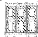
- FIG. 2 is a partial plan sectional view of the surface acoustic wave device assembly according to the first embodiment of the present invention.
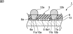
- FIG. 3 is a front sectional view of the surface acoustic wave device according to the first embodiment of the present invention.
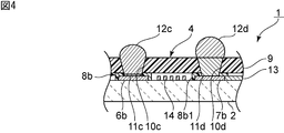
- FIG. 4 is a front sectional view of the evaluation element in the first embodiment of the present invention.
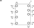
- FIG. 5 is a plan view of the surface acoustic wave device according to the first embodiment of the present invention.
- FIG. 6 is a plan view of an evaluation element according to the first embodiment of the present invention.
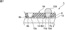
- FIG. 7 is a front cross-sectional view of an evaluation element in a modification of the first embodiment of the present invention.
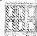
- FIG. 8 is a partial plan sectional view of the surface acoustic wave device assembly according to the second embodiment of the present invention.
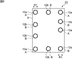
- FIG. 9 is a plan view of the surface acoustic wave device according to the second embodiment of the present invention.
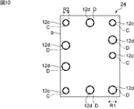
- FIG. 10 is a plan view of an evaluation element according to the second embodiment of the present invention.
- FIG. 11 shows a state in which the surface acoustic wave device assembly is fixed with a tape in the back grinding process of the aggregate substrate used in the surface acoustic wave device assembly according to the second embodiment of the present invention.
- FIG. 11 shows a state in which the surface acoustic wave device assembly is fixed with a tape in the back grinding process of the aggregate substrate used in the surface acoustic wave device assembly according to the second embodiment of the present invention.
- FIGS. 12 (a) to 12 (e) are views for explaining a method of manufacturing a surface acoustic wave device assembly as a third embodiment of the present invention.
- FIGS. 13 (a) to 13 (d) are views for explaining a method of manufacturing a surface acoustic wave device assembly as a third embodiment of the present invention.
- FIGS. 14 (a) to 14 (c) are views for explaining a method of manufacturing a surface acoustic wave device assembly as a third embodiment of the present invention.
- FIG. 1 is a partial front view of a surface acoustic wave device assembly according to a first embodiment of the present invention.
- FIG. 2 is a partial plan sectional view of the surface acoustic wave device assembly according to the first embodiment of the present invention.
- the surface acoustic wave device assembly 1 has a collective substrate 2.
- the collective substrate 2 is a LiTaO 3 substrate having a cut angle of 42 °.
- the collective substrate 2 is not limited to the above-described piezoelectric body, and may be made of another piezoelectric single crystal such as LiNbO 3 or an appropriate piezoelectric ceramic.
- the surface acoustic wave device assembly 1 includes a plurality of first circuit portions 3 ⁇ / b> A configured on a collective substrate 2. Each first circuit unit 3A constitutes a surface acoustic wave device 3 that is a band-pass filter.
- the surface acoustic wave device assembly 1 also includes a second circuit unit 4A configured on the collective substrate 2.
- the second circuit unit 4A constitutes an evaluation element 4 that is a band-pass filter. In the present embodiment, the evaluation element 4 is also a surface acoustic wave device.
- each of the first circuit unit 3A and the second circuit unit 4A are the same. That is, the arrangement and material of each element and wiring constituting each surface acoustic wave device 3 are the same as the arrangement and material of each element and wiring constituting the evaluation element 4. Therefore, the pass band of each surface acoustic wave device 3 and the pass band of the evaluation element 4 are the same.
- a power supply wiring 13 is provided on the collective substrate 2 so as to surround each surface acoustic wave device 3 and the evaluation element 4.
- the power supply wiring 13 is provided along a dicing line that is divided into individual surface acoustic wave devices.
- the power supply wiring 13 is a wiring for forming an under bump metal layer described later by an electrolytic plating method.
- Each surface acoustic wave device 3 has a first support member 8a provided on the collective substrate 2 so as to surround the first circuit portion 3A.
- Each first circuit portion 3A faces the first opening 8a1 of each first support member 8a.
- the evaluation element 4 includes a second support member 8b provided on the collective substrate 2 so as to surround the second circuit portion 4A.
- the second circuit portion 4A faces the second opening 8b1 of the second support member 8b.
- the plurality of first support members 8a and second support members 8b are made of resin or the like.
- Each surface acoustic wave device 3 has a plurality of first hot terminals 6a and a plurality of first ground terminals 7a provided on the collective substrate 2.
- the first hot terminal 6 a and the first ground terminal 7 a are connected to the power supply wiring 13.
- the evaluation element 4 includes a plurality of second hot terminals 6b and a plurality of second ground terminals 7b provided on the collective substrate 2.
- the second ground terminal 7 b is connected to the power supply wiring 13.
- the second hot terminal 6 b is not connected to the power supply wiring 13.
- each first hot terminal 6a in each surface acoustic wave device 3 and the position of the second hot terminal 6b in the evaluation element 4 are the same.
- the position of each first ground terminal 7a in each surface acoustic wave device 3 and the position of the second ground terminal 7b in evaluation element 4 are the same.
- FIG. 3 is a front sectional view of the surface acoustic wave device according to the first embodiment of the present invention.
- the surface acoustic wave device 3 has an IDT electrode 5 provided on the collective substrate 2.
- the first circuit portion 3A shown in FIG. 2 is composed of a plurality of IDT electrodes.
- the IDT electrode 5 is connected to the first hot terminal 6a and the first ground terminal 7a.
- the first support member 8a is provided on the collective substrate 2 so as to cover the first hot terminal 6a and the first ground terminal 7a.
- a lid member 9 is provided so as to seal the first opening 8a1 of the first support member 8a.
- the lid member 9 is made of resin or the like.
- First and second through holes 10a and 10b are provided so as to penetrate the lid member 9 and the first support member 8a.
- One end of the first through hole 10a reaches the first hot terminal 6a.
- One end of the second through hole 10b reaches the first ground terminal 7a.
- a first under bump metal layer 11a is provided in the first through hole 10a.
- a second under bump metal layer 11b is provided in the second through hole 10b.
- a first bump 12a is provided on the first under bump metal layer 11a.
- a second bump 12b is provided on the second under bump metal layer 11b.
- the first under bump metal layer 11a connects the first hot terminal 6a and the first bump 12a.
- the second under bump metal layer 11b connects the first ground terminal 7a and the second bump 12b.
- the first and second bumps 12a and 12b are made of an appropriate brazing filler metal such as solder.
- first through holes and first under bump metal layers are provided so as to be connected to a plurality of first hot terminals, respectively.
- a plurality of second through holes and second under bump metal layers are provided so as to be connected to the plurality of first ground terminals, respectively.
- FIG. 4 is a front sectional view of the evaluation element according to the first embodiment of the present invention.
- the evaluation element 4 has a functional electrode 14 provided on the collective substrate 2.
- the second circuit unit 4A illustrated in FIG. In the present embodiment, the evaluation element 4 has the same electrical circuit configuration as the surface acoustic wave device 3.
- the functional electrode 14 is an IDT electrode similar to the IDT electrode 5 of the surface acoustic wave device 3 shown in FIG.
- the functional electrode 14 is connected to the second hot terminal 6b and the second ground terminal 7b.
- the second support member 8b is provided on the collective substrate 2 so as to cover the second hot terminal 6b and the second ground terminal 7b.
- a lid member 9 is provided so as to seal the second opening 8b1 of the second support member 8b.
- the third and fourth through holes 10c and 10d are provided so as to penetrate the lid member 9 and the second support member 8b.
- One end of the third through hole 10c reaches the second hot terminal 6b.
- One end of the fourth through hole 10d reaches the second ground terminal 7b.
- the arrangement of the first through hole 10a and the second through hole 10b in the first support member 8a shown in FIG. 3, and the third through hole 10c and the fourth through hole 10d in the second support member 8b are shown. The arrangement is the same.
- a third under bump metal layer 11c is provided in the third through hole 10c.
- a fourth under bump metal layer 11d is provided in the fourth through hole 10d.
- the thickness of the fourth under bump metal layer 11d is larger than the thickness of the third under bump metal layer 11c.
- the thicknesses of the first and second under bump metal layers 11a and 11b shown in FIG. 3 are also larger than the thickness of the third under bump metal layer 11c. Note that the third under bump metal layer 11c may not be provided.
- the third bump 12c is provided on the third under bump metal layer 11c.
- a fourth bump 12d is provided on the fourth under bump metal layer 11d.
- the third under bump metal layer 11c connects the second hot terminal 6b and the third bump 12c.
- the fourth under bump metal layer 11d connects the second ground terminal 7b and the fourth bump 12d.
- the third and fourth bumps 12c and 12d are made of an appropriate brazing filler metal such as solder.
- the third bump 12c only needs to be provided at a position overlapping the third through hole 10c in plan view.
- the third bump 12c and the third under bump metal layer 11c may not be connected.
- a plurality of third through holes and third under bump metal layers are provided so as to be connected to a plurality of second hot terminals, respectively.
- a plurality of fourth through holes and fourth under bump metal layers are provided so as to be connected to a plurality of second ground terminals, respectively.
- the feature of the present embodiment is that the surface acoustic wave device assembly 1 has the evaluation element 4 and the second hot terminal 6 b of the evaluation element 4 is not connected to the power supply wiring 13. According to this embodiment, a good product and a defective product can be selected before being divided into individual surface acoustic wave devices. This will be described below.
- the electrical circuit configuration and physical configuration of the first circuit unit 3A of the plurality of surface acoustic wave devices 3 and the second circuit unit 4A of the evaluation element 4 are the same. Therefore, the plurality of surface acoustic wave devices 3 on the same collective substrate 2 have substantially the same electrical characteristics as the evaluation element 4 on the same collective substrate 2. Therefore, if the electrical characteristics such as the filter characteristics of the evaluation element 4 are inspected and it is determined that the performance as a non-defective product is not satisfied, the plurality of surface acoustic wave devices 3 on the same collective substrate 2 are also regarded as non-defective products. It can be determined that the performance is not satisfied.
- the electrical circuit configuration and physical configuration of the evaluation element 4 and the plurality of surface acoustic wave devices 3 are preferably the same as in this embodiment. As a result, the non-defective product can be more reliably selected.
- the evaluation element 4 may be inspected for electrical characteristics, for example, after the second circuit portion 4A is provided and before the second support member 8b is provided. Thereby, it is possible to select a good product and a defective product before being divided into individual surface acoustic wave devices 3. Therefore, since only the plurality of surface acoustic wave devices 3 determined as non-defective products can be put into the subsequent process, the cost can be reduced.
- the second hot terminal 6 b of the evaluation element 4 is not connected to the power supply wiring 13. Therefore, when the first to fourth under bump metal layers 11a to 11d shown in FIGS. 3 and 4 are formed by the electrolytic plating method, the third under bump metal layer 11c is not sufficiently formed. Therefore, the thickness of the third under bump metal layer 11c is smaller than the thickness of the first, second, and fourth under bump metal layers 11a, 11b, and 11d.
- the first, second, and fourth bumps 12a, 12b, and 12d are provided on the first, second, and fourth under bump metal layers 11a, 11b, and 11d having a large thickness.
- the first, second, and fourth bumps 12a, 12b, and 12d do not greatly enter the first, second, and fourth through holes 10a, 10b, and 10d.
- the third bumps 12c provided on the third under bump metal layer 11c having a small thickness greatly enter the third through hole 10c.
- FIG. 5 is a plan view of the surface acoustic wave device according to the first embodiment of the present invention.
- FIG. 6 is a plan view of the evaluation element in the first embodiment.
- Inscribed circles inscribed in the first to fourth bumps 12a to 12d are inscribed circles A to D. Since only the third bump 12c has entered the third through hole 10c, the diameter R2 of the inscribed circle C is smaller than the diameter R1 of the inscribed circles A, B, and D. Thus, from the difference between the diameter R2 of the inscribed circle C and the diameter R1 of the inscribed circles A, B, D, whether the surface acoustic wave device 3 is a plurality of surface acoustic wave devices 3 or the evaluation element 4 in plan view. Can be easily identified. Therefore, only the evaluation element 4 can be easily removed after being divided into the individual surface acoustic wave devices 3.
- each first circuit unit 3A and the second circuit unit 4A may be the same, and the physical configuration may be different. Even in this case, if there is a correlation between the electrical characteristics of each surface acoustic wave device 3 and the electrical characteristics of the evaluation element 4, it is possible to select a non-defective product and a defective product of the plurality of surface acoustic wave devices 3. it can.
- the electrical circuit configuration and physical configuration of the first circuit unit 3A and the second circuit unit 4A are the same. If the pass band of each surface acoustic wave device 3 and the pass band of the evaluation element 4 are the same, the electrical circuit configuration and physical properties of each of the first circuit unit 3A and the second circuit unit 4A The general configuration may be different.
- the electrical circuit configuration of the first circuit unit 3A and the second circuit unit 4A And the physical configuration may be different.
- each surface acoustic wave device 3 and the evaluation element 4 are band-pass filters. Therefore, when selecting the non-defective product of the surface acoustic wave device 3, the filter characteristics and the like are inspected.
- Each surface acoustic wave device 3 and the evaluation element 4 are not limited to band-pass filters, and may be resonators, for example. In this case, for example, impedance characteristics and the like may be inspected.
- the functional electrode 14 of the evaluation element 4 is an IDT electrode, but if there is a correlation between the electrical characteristics of the evaluation element 4 and the electrical characteristics of each surface acoustic wave device 3, the functional electrode 14 is It may not be an IDT electrode. That is, the evaluation element 4 is not necessarily a surface acoustic wave device.
- the evaluation element 54 may not be provided with the third under bump metal layer. Since the evaluation element 54 is not provided with the third under bump metal layer, the third bump is not provided. Also in this case, it is possible to select a non-defective product and a defective product of the plurality of surface acoustic wave devices by inspecting the electrical characteristics of the evaluation element 54, and the plurality of surface acoustic wave devices in a plan view. Or the evaluation element 54 can be easily identified. The same effect as that of the first embodiment can be obtained even in the configuration in which the third under bump metal layer is provided in the third through hole and the third bump is not provided.
- FIG. 8 is a partial plan sectional view of the surface acoustic wave device assembly according to the second embodiment of the present invention.
- FIG. 9 is a plan view of the surface acoustic wave device according to the second embodiment.
- FIG. 10 is a plan view of an evaluation element according to the second embodiment.
- This embodiment is different from the first embodiment in that more ground terminals are arranged than hot terminals. More specifically, the second ground terminals 7b of the evaluation element 24 in the surface acoustic wave device assembly 21 are arranged more than the second hot terminals 6b. Therefore, the fourth bumps 12d that are electrically connected to the second ground terminal 7b are arranged more than the third bumps 12c that are electrically connected to the second hot terminal 6b.
- the first ground terminals 7a of the plurality of surface acoustic wave devices 23 are arranged more than the first hot terminals 6a. Therefore, the second bumps 12b that are electrically connected to the first ground terminal 7a are arranged more than the first bumps 12a that are electrically connected to the first hot terminal 6a.
- the third bump 12 c greatly enters the third through hole 10 c. Therefore, the thickness of the third bump 12c in the direction toward the outside of the third through hole 10c with reference to the main surface of the lid member 9 opposite to the second support member 8b side is the fourth bump 12d. Is less than the above thickness.
- the 1st, 2nd bump 12a in the direction which goes outside the 1st through-hole 10a on the basis of the main surface on the opposite side to the 1st support member 8a side of the cover member 9 shown in FIG. , 12b and the thickness of the fourth bump 12d are approximately the same.
- FIG. 11 shows a state in which the surface acoustic wave device assembly is fixed with a tape in the back grinding process of the aggregate substrate used in the surface acoustic wave device assembly according to the second embodiment of the present invention.
- the aggregate substrate 2 is provided with, for example, first and second ground terminals 7a and 7b and first and second hot terminals 6a and 6b after first to fourth bumps 12a to 12d are provided. It is half-cut from the main surface. Thereafter, the aggregate substrate 2 is divided into individual piezoelectric substrates by grinding the main surface opposite to the main surface. Thereby, the surface acoustic wave device assembly 21 is divided into individual surface acoustic wave devices 23. As described above, in this embodiment, the posture when grinding the collective substrate 2 can be stabilized. Therefore, the flatness of the divided piezoelectric substrate can be effectively increased, and the variation in thickness of each piezoelectric substrate can be effectively reduced.
- FIGS. 14 (a) to 14 (c) are views for explaining a method of manufacturing a surface acoustic wave device assembly as a third embodiment of the present invention.
- 12 (a) to 12 (e) and FIGS. 13 (a) to 13 (d) one surface acoustic wave device among a plurality of surface acoustic wave devices in the surface acoustic wave device assembly and The manufacturing method of the element for evaluation is shown.
- a collective substrate 2 is prepared.
- the IDT electrode 5, the functional electrode 14, the first and second hot terminals 6 a and 6 b, the first and second ground terminals 7 a and 7 b, and the power supply wiring 13 are provided on the collective substrate 2.
- the first hot terminal 6 a and the first ground terminal 7 a are provided so as to be connected to the IDT electrode 5.
- the second hot terminal 6 b and the second ground terminal 7 b are provided so as to be connected to the functional electrode 14.
- the first and second hot terminals 6a and 6b are provided so that the position of the first hot terminal 6a in the surface acoustic wave device 43 and the position of the second hot terminal 6b in the evaluation element 44 are the same.
- the first and second ground terminals 7a and 7b are provided so that the position of the first ground terminal 7a in the surface acoustic wave device 43 and the position of the second ground terminal 7b in the evaluation element 44 are the same. Thereby, the manufacturing process can be simplified.
- the power supply wiring 13 is provided along the dicing line I that divides the collective substrate in a later process.
- the power supply wiring 13 is provided so as to be connected to the first hot terminal 6a and the first and second ground terminals 7a and 7b but not to the second hot terminal 6b.
- the IDT electrode 5, the functional electrode 14, the first and second hot terminals 6a and 6b, the first and second ground terminals 7a and 7b, and the power supply wiring 13 can be formed by, for example, a CVD method or a sputtering method. it can.
- wirings 46 and 47 as second layer electrodes are formed on the first and second hot terminals 6a and 6b and on the first and second ground terminals 7a and 7b.
- the wirings 46 and 47 can be formed by, for example, a CVD method or a sputtering method. Note that the wirings 46 and 47 are not necessarily formed. However, by forming the wirings 46 and 47, the electrical resistances of the first and second hot terminals 6a and 6b and the first and second ground terminals 7a and 7b can be reduced. Therefore, it is preferable to form the wirings 46 and 47.
- a protective film 45 is provided on the collective substrate 2 so as to cover the IDT electrode 5 and the functional electrode 14.
- Protective film 45 is made of a dielectric material such as SiO 2.
- the protective film 45 can be formed by, for example, a CVD method. Note that the protective film 45 is not necessarily provided. However, providing the protective film 45 can make it difficult to damage the IDT electrode 5 and the functional electrode 14. Therefore, it is preferable to provide the protective film 45.
- the electrical characteristics of the evaluation element 44 are inspected.
- a part of the protective film 45 is removed so that at least the first and second hot terminals 6a and 6b and the first and second ground terminals 7a and 7b have exposed portions.
- Inspection is performed by bringing the probe X and probe Y of the inspection apparatus into contact with the wiring 46 on the second hot terminal 6b and the wiring 47 on the second ground terminal 7b at the exposed portion.
- the non-defective product and the defective product of the plurality of surface acoustic wave devices 43 can be selected. Since only the plurality of surface acoustic wave devices 43 on the aggregate substrate 2 on which the evaluation element 44 determined to satisfy the desired characteristics by the inspection can be put into the subsequent process, the cost is reduced. be able to.
- the first support member 8 a is provided on the collective substrate 2 so as to cover the first hot terminal 6 a and the first ground terminal 7 a and surround the IDT electrode 5.
- a second support member 8b is provided on the collective substrate 2 so as to cover the second hot terminal 6b and the second ground terminal 7b and surround the functional electrode 14.
- the planar shape of the first opening 8a1 of the first support member 8a facing the IDT electrode 5 and the planar shape of the second opening 8b1 of the second supporting member 8b facing the functional electrode 14 are the same.
- the first and second support members 8a and 8b are provided. Thereby, the manufacturing process can be simplified. Note that the planar shape of the first opening 8a1 and the planar shape of the second opening 8b1 may not be the same.
- the first and second support members 8a and 8b can be provided by, for example, a photolithography method.
- the lid member 9 is sealed so as to seal the first opening 8a1 of the first support member 8a and the second opening 8b1 of the second support member 8b. Is provided.
- the first through hole 10a is provided so as to penetrate the lid member 9 and the first support member 8a and reach the wiring 46 on the first hot terminal 6a.
- a second through hole 10b is provided so as to penetrate the lid member 9 and the first support member 8a and reach the wiring 47 on the first ground terminal 7a.
- a third through hole 10c is provided so as to penetrate the lid member 9 and the second support member 8b and reach the wiring 46 on the second hot terminal 6b.
- a fourth through hole 10d is provided so as to penetrate the lid member 9 and the second support member 8b and reach the wiring 47 on the second ground terminal 7b.
- the first and second hot terminals 6a are arranged so that the position of the first hot terminal 6a in the surface acoustic wave device 43 and the position of the second hot terminal 6b in the evaluation element 44 are the same.
- 6b are provided. Therefore, the first and third through holes 10a are arranged so that the arrangement of the first through holes 10a in the first support member 8a and the arrangement of the third through holes 10c in the second support member 8b are the same. , 10c.
- the first and second ground terminals 7a and 7b are provided so that the position of the first ground terminal 7a in the first circuit portion and the position of the second ground terminal 7b in the second circuit portion are the same. It has been.
- the second and fourth through holes 10b are arranged so that the arrangement of the second through holes 10b in the first support member 8a is the same as the arrangement of the fourth through holes 10d in the second support member 8b. , 10d. Thereby, the manufacturing process can be simplified.
- first to fourth under bump metal layers 11a to 11d are provided in the first to fourth through holes 10a to 10d.
- the first, second, and fourth under bump metal layers 11a, 11b, and 11d are electrolyzed using a power supply wiring 13 connected to the first hot terminal 6a and the first and second ground terminals 7a and 7b. It can be formed by a plating method.
- the second hot terminal 6 b is not connected to the power supply wiring 13. Therefore, the third under bump metal layer 11c is not formed by the electrolytic plating method using the power supply wiring 13 directly.
- the wiring 46 on the second hot terminal 6b exposed through the third through hole 10c is electroplated to form the third under bump metal layer 11c.
- the third under bump metal layer 11c need not be provided. Therefore, a structure or manufacturing method in which the leakage current is less likely to occur may be used.
- the first to fourth bumps 12a to 12d are provided on the first to fourth under bump metal layers 11a to 11d.
- the third bump 12c may not be provided.
- the amount of brazing filler metal used for bumps can be reduced.
- the manufacturing process can be simplified by providing the first to fourth bumps under the same conditions as in this embodiment.
- a dicing line I is formed from the main surface on the side where the first and second ground terminals 7a and 7b and the first and second hot terminals 6a and 6b are provided. A half cut is performed at.
- the surface acoustic wave device assembly is fixed to the tape 35. More specifically, the first, second, and fourth bumps 12a, 12b, and 12d are attached to the tape 35.
- the main surface opposite to the main surface of the collective substrate 2 is ground. Accordingly, as shown in FIG. 14C, the collective substrate 2 shown in FIG. 14B is divided into individual piezoelectric substrates 42, and is divided into individual surface acoustic wave devices 43 and evaluation elements 44.
- the portion supporting the tape 35 can be increased. Thereby, the posture of grinding the collective substrate 2 can be effectively stabilized. Therefore, the flatness of each piezoelectric substrate 42 can be effectively increased, and thickness variations can be effectively reduced.
- a full cut is made from the main surface on the side where the first and second ground terminals 7a and 7b and the first and second hot terminals 6a and 6b are provided. You may go.
Landscapes
- Physics & Mathematics (AREA)
- Acoustics & Sound (AREA)
- Engineering & Computer Science (AREA)
- Manufacturing & Machinery (AREA)
- Surface Acoustic Wave Elements And Circuit Networks Thereof (AREA)
Abstract
Description
2…集合基板
3…弾性表面波装置
3A…第1の回路部
4…評価用素子
4A…第2の回路部
5…IDT電極
6a,6b…第1,第2のホット端子
7a,7b…第1,第2のグラウンド端子
8a,8b…第1,第2の支持部材
8a1,8b1…第1,第2の開口部
9…蓋部材
10a~10d…第1~第4の貫通孔
11a~11d…第1~第4のアンダーバンプメタル層
12a~12d…第1~第4のバンプ
13…給電配線
14…機能電極
21…弾性表面波装置集合体
23…弾性表面波装置
24…評価用素子
35…テープ
42…圧電基板
43…弾性表面波装置
44…評価用素子
45…保護膜
46,47…配線
54…評価用素子
X,Y…プローブ
Claims (11)
- 圧電体からなる集合基板と、
前記集合基板上に設けられており、IDT電極と、前記IDT電極に接続されている第1のホット端子及び第1のグラウンド端子とをそれぞれ有する複数の第1の回路部と、
前記集合基板上に設けられており、機能電極と、前記機能電極に接続されている第2のホット端子及び第2のグラウンド端子とを有する第2の回路部と、
前記複数の第1の回路部及び前記第2の回路部の周囲を囲むように前記集合基板上に設けられている給電配線と、
を備え、
各前記第1の回路部は、帯域通過型フィルタである弾性表面波装置をそれぞれ構成しており、前記第2の回路部は帯域通過型フィルタを構成しており、
複数の前記第1のグラウンド端子及び複数の前記第1のホット端子が前記給電配線に接続されており、前記第2のグラウンド端子が前記給電配線に接続されており、前記第2のホット端子が前記給電配線に接続されておらず、
各前記弾性表面波装置の通過帯域と、前記第2の回路部により構成されている帯域通過型フィルタの通過帯域とが同一である、弾性表面波装置集合体。 - 圧電体からなる集合基板と、
前記集合基板上に設けられており、IDT電極と、前記IDT電極に接続されている第1のホット端子及び第1のグラウンド端子とをそれぞれ有する複数の第1の回路部と、
前記集合基板上に設けられており、機能電極と、前記機能電極に接続されている第2のホット端子及び第2のグラウンド端子とを有する第2の回路部と、
前記複数の第1の回路部及び前記第2の回路部の周囲を囲むように前記集合基板上に設けられている給電配線と、
を備え、
各前記第1の回路部は、弾性表面波装置をそれぞれ構成しており、
複数の前記第1のグラウンド端子及び複数の前記第1のホット端子が前記給電配線に接続されており、前記第2のグラウンド端子が前記給電配線に接続されており、前記第2のホット端子が前記給電配線に接続されておらず、
前記複数の第1の回路部の電気的な回路構成と前記第2の回路部の電気的な回路構成とが同一である、弾性表面波装置集合体。 - 前記集合基板上に設けられており、各前記第1の回路部が臨む第1の開口部をそれぞれ有する複数の第1の支持部材と、
前記集合基板上に設けられており、前記第2の回路部が臨む第2の開口部を有する第2の支持部材と、
複数の前記第1の開口部及び前記第2の開口部を封止するように、前記複数の第1の支持部材上及び前記第2の支持部材上に設けられている蓋部材と、
をさらに備え、
前記複数の第1の支持部材は、平面視において、前記複数の第1のホット端子及び前記複数の第1のグラウンド端子と重なるように設けられており、前記第2の支持部材は、前記第2のホット端子及び前記第2のグラウンド端子と重なるように設けられており、
前記第1の支持部材及び前記蓋部材を貫通し、前記複数の第1のホット端子及び前記複数の第1のグラウンド端子を露出させるように複数の第1の貫通孔及び複数の第2の貫通孔が設けられており、前記第2の支持部材及び前記蓋部材を貫通し、前記第2のホット端子及び前記第2のグラウンド端子が露出するように第3の貫通孔及び第4の貫通孔が設けられている、請求項1または2に記載の弾性表面波装置集合体。 - 前記複数の第1の貫通孔にそれぞれ設けられている第1のアンダーバンプメタル層と、
前記複数の第2の貫通孔にそれぞれ設けられている第2のアンダーバンプメタル層と、
前記第4の貫通孔に設けられている第4のアンダーバンプメタル層と、
をさらに備える、請求項3に記載の弾性表面波装置集合体。 - 前記第3の貫通孔にアンダーバンプメタル層が設けられていない、請求項4に記載の弾性表面波装置集合体。
- 前記第3の貫通孔に設けられている第3のアンダーバンプメタル層をさらに備え、
各前記第1のアンダーバンプメタル層の厚みが前記第3のアンダーバンプメタル層の厚みよりも大きい、請求項4に記載の弾性表面波装置集合体。 - 各前記第1のアンダーバンプメタル層上に設けられている複数の第1のバンプと、
各前記第2のアンダーバンプメタル層上に設けられている複数の第2のバンプと、
平面視において前記第3の貫通孔と重なる位置に設けられている第3のバンプと、
前記第4のアンダーバンプメタル層上に設けられている第4のバンプと、
をさらに備え、
平面視において、各前記第1のバンプに内接する内接円の直径が、前記第3のバンプに内接する内接円の直径よりも大きい、請求項6に記載の弾性表面波装置集合体。 - 各前記第1の支持部材の各前記第1の開口部の平面形状と、前記第2の支持部材の前記第2の開口部の平面形状とが同一である、請求項3~7のいずれか1項に記載の弾性表面波装置集合体。
- 前記第2のグラウンド端子が前記第2のホット端子よりも多く配置されている、請求項3~8のいずれか1項に記載の弾性表面波装置集合体。
- 各前記第1の支持部材における前記第1及び第2の貫通孔の配置と、前記第2の支持部材における前記第3及び第4の貫通孔の配置とが同一である、請求項3~9のいずれか1項に記載の弾性表面波装置集合体。
- 前記第2の回路部の前記機能電極が前記複数の第1の回路部の前記IDT電極と同様の構成を有するIDT電極であり、前記複数の第1の回路部と前記第2の回路部との電気的な回路構成及び物理的な構成が同一である、請求項1~10のいずれか1項に記載の弾性表面波装置集合体。
Priority Applications (4)
| Application Number | Priority Date | Filing Date | Title |
|---|---|---|---|
| KR1020177021717A KR101949067B1 (ko) | 2015-02-03 | 2016-02-01 | 탄성 표면파 장치 집합체 |
| JP2016573356A JP6315111B2 (ja) | 2015-02-03 | 2016-02-01 | 弾性表面波装置集合体 |
| CN201680006223.6A CN107210726B (zh) | 2015-02-03 | 2016-02-01 | 声表面波装置集合体 |
| US15/651,036 US10622965B2 (en) | 2015-02-03 | 2017-07-17 | Surface acoustic wave device assembly |
Applications Claiming Priority (2)
| Application Number | Priority Date | Filing Date | Title |
|---|---|---|---|
| JP2015019603 | 2015-02-03 | ||
| JP2015-019603 | 2015-02-03 |
Related Child Applications (1)
| Application Number | Title | Priority Date | Filing Date |
|---|---|---|---|
| US15/651,036 Continuation US10622965B2 (en) | 2015-02-03 | 2017-07-17 | Surface acoustic wave device assembly |
Publications (1)
| Publication Number | Publication Date |
|---|---|
| WO2016125753A1 true WO2016125753A1 (ja) | 2016-08-11 |
Family
ID=56564096
Family Applications (1)
| Application Number | Title | Priority Date | Filing Date |
|---|---|---|---|
| PCT/JP2016/052952 Ceased WO2016125753A1 (ja) | 2015-02-03 | 2016-02-01 | 弾性表面波装置集合体 |
Country Status (5)
| Country | Link |
|---|---|
| US (1) | US10622965B2 (ja) |
| JP (1) | JP6315111B2 (ja) |
| KR (1) | KR101949067B1 (ja) |
| CN (1) | CN107210726B (ja) |
| WO (1) | WO2016125753A1 (ja) |
Families Citing this family (4)
| Publication number | Priority date | Publication date | Assignee | Title |
|---|---|---|---|---|
| WO2015022931A1 (ja) * | 2013-08-14 | 2015-02-19 | 株式会社村田製作所 | 弾性波装置、電子部品、および弾性波装置の製造方法 |
| KR101754200B1 (ko) * | 2013-08-20 | 2017-07-05 | 가부시키가이샤 무라타 세이사쿠쇼 | 탄성 표면파 디바이스 및 그 제조 방법 |
| US12191838B2 (en) * | 2018-06-15 | 2025-01-07 | Murata Manufacturing Co., Ltd. | Solidly-mounted transversely-excited film bulk acoustic device and method |
| US12191837B2 (en) * | 2018-06-15 | 2025-01-07 | Murata Manufacturing Co., Ltd. | Solidly-mounted transversely-excited film bulk acoustic device |
Citations (4)
| Publication number | Priority date | Publication date | Assignee | Title |
|---|---|---|---|---|
| JP2006120962A (ja) * | 2004-10-25 | 2006-05-11 | Nec Electronics Corp | 半導体装置及びその製造方法 |
| JP2007028195A (ja) * | 2005-07-15 | 2007-02-01 | Murata Mfg Co Ltd | 弾性境界波装置及びその製造方法 |
| JP2008028199A (ja) * | 2006-07-21 | 2008-02-07 | Nichicon Corp | 混成集積回路基板の製造方法 |
| JP2009206183A (ja) * | 2008-02-26 | 2009-09-10 | Fujitsu Media Device Kk | 電子部品及びその製造方法 |
Family Cites Families (14)
| Publication number | Priority date | Publication date | Assignee | Title |
|---|---|---|---|---|
| JPH08335616A (ja) * | 1995-06-06 | 1996-12-17 | Nippon Inter Electronics Corp | 半導体装置及びその検査方法 |
| JPH0955398A (ja) * | 1995-08-10 | 1997-02-25 | Murata Mfg Co Ltd | 半導体装置の製造方法 |
| JP3290140B2 (ja) | 1998-07-22 | 2002-06-10 | 東洋通信機株式会社 | 弾性表面波デバイスの製造方法 |
| JP2002232254A (ja) | 2001-01-31 | 2002-08-16 | Kyocera Corp | 弾性表面波装置 |
| JP4518870B2 (ja) * | 2004-08-24 | 2010-08-04 | 京セラ株式会社 | 弾性表面波装置および通信装置 |
| JP4877465B2 (ja) * | 2005-08-03 | 2012-02-15 | セイコーエプソン株式会社 | 半導体装置、半導体装置の検査方法、半導体ウェハ |
| WO2007125724A1 (ja) | 2006-04-28 | 2007-11-08 | Murata Manufacturing Co., Ltd. | 電子部品及びその製造方法 |
| WO2010047031A1 (ja) * | 2008-10-24 | 2010-04-29 | 株式会社 村田製作所 | 電子部品、およびその製造方法 |
| KR101655302B1 (ko) * | 2009-09-22 | 2016-09-07 | 삼성전자주식회사 | 표면 탄성파 센서 시스템 |
| JP5654303B2 (ja) * | 2010-09-21 | 2015-01-14 | 太陽誘電株式会社 | 電子部品およびその製造方法、並びに電子部品を備えた電子デバイス |
| WO2012050016A1 (ja) | 2010-10-15 | 2012-04-19 | 株式会社村田製作所 | 弾性表面波装置 |
| JP5766457B2 (ja) * | 2011-02-09 | 2015-08-19 | 太陽誘電株式会社 | 弾性波デバイス及びその製造方法 |
| JP5666366B2 (ja) * | 2011-03-31 | 2015-02-12 | ルネサスエレクトロニクス株式会社 | 半導体装置の製造方法 |
| KR101804496B1 (ko) * | 2013-07-17 | 2017-12-04 | 가부시키가이샤 무라타 세이사쿠쇼 | 전자부품 및 그 제조방법 |
-
2016
- 2016-02-01 KR KR1020177021717A patent/KR101949067B1/ko not_active Expired - Fee Related
- 2016-02-01 WO PCT/JP2016/052952 patent/WO2016125753A1/ja not_active Ceased
- 2016-02-01 JP JP2016573356A patent/JP6315111B2/ja not_active Expired - Fee Related
- 2016-02-01 CN CN201680006223.6A patent/CN107210726B/zh not_active Expired - Fee Related
-
2017
- 2017-07-17 US US15/651,036 patent/US10622965B2/en active Active
Patent Citations (4)
| Publication number | Priority date | Publication date | Assignee | Title |
|---|---|---|---|---|
| JP2006120962A (ja) * | 2004-10-25 | 2006-05-11 | Nec Electronics Corp | 半導体装置及びその製造方法 |
| JP2007028195A (ja) * | 2005-07-15 | 2007-02-01 | Murata Mfg Co Ltd | 弾性境界波装置及びその製造方法 |
| JP2008028199A (ja) * | 2006-07-21 | 2008-02-07 | Nichicon Corp | 混成集積回路基板の製造方法 |
| JP2009206183A (ja) * | 2008-02-26 | 2009-09-10 | Fujitsu Media Device Kk | 電子部品及びその製造方法 |
Also Published As
| Publication number | Publication date |
|---|---|
| CN107210726A (zh) | 2017-09-26 |
| JPWO2016125753A1 (ja) | 2017-04-27 |
| US10622965B2 (en) | 2020-04-14 |
| KR20170101993A (ko) | 2017-09-06 |
| KR101949067B1 (ko) | 2019-02-15 |
| US20170317659A1 (en) | 2017-11-02 |
| CN107210726B (zh) | 2020-10-23 |
| JP6315111B2 (ja) | 2018-04-25 |
Similar Documents
| Publication | Publication Date | Title |
|---|---|---|
| US10250219B2 (en) | Acoustic wave device | |
| US11031919B2 (en) | Elastic wave device, duplexer, and communication device | |
| US10707830B2 (en) | Elastic wave device and method for manufacturing the same | |
| JP6397352B2 (ja) | 弾性波デバイス | |
| JP6315111B2 (ja) | 弾性表面波装置集合体 | |
| CN106716827B (zh) | 压电模块 | |
| CN105814796A (zh) | 弹性波滤波器设备 | |
| US11177788B2 (en) | Acoustic wave device, radio frequency front-end module, and communication device | |
| US9065420B2 (en) | Fabrication method of acoustic wave device | |
| US10951194B2 (en) | Acoustic wave filter, multiplexer, and communication apparatus | |
| KR20190074213A (ko) | 탄성파 장치 | |
| KR102632356B1 (ko) | 음향 공진기 및 그 제조 방법 | |
| US11177789B2 (en) | Acoustic wave device and method of manufacturing the same | |
| JP6166190B2 (ja) | 弾性波素子および弾性波装置 | |
| JP4722204B2 (ja) | 弾性表面波装置及び弾性表面波装置の製造方法 | |
| JP5500316B2 (ja) | 電子部品の製造方法 | |
| JP2014230079A (ja) | 弾性表面波装置 | |
| JP2014216971A (ja) | 弾性表面波装置 | |
| CN119341496A (zh) | 弹性波装置以及弹性波装置的制造方法 | |
| KR20230010466A (ko) | Saw 필터 | |
| KR20190138104A (ko) | 표면탄성파 소자 패키지 및 그 제작 방법 |
Legal Events
| Date | Code | Title | Description |
|---|---|---|---|
| 121 | Ep: the epo has been informed by wipo that ep was designated in this application |
Ref document number: 16746584 Country of ref document: EP Kind code of ref document: A1 |
|
| ENP | Entry into the national phase |
Ref document number: 2016573356 Country of ref document: JP Kind code of ref document: A |
|
| ENP | Entry into the national phase |
Ref document number: 20177021717 Country of ref document: KR Kind code of ref document: A |
|
| NENP | Non-entry into the national phase |
Ref country code: DE |
|
| 122 | Ep: pct application non-entry in european phase |
Ref document number: 16746584 Country of ref document: EP Kind code of ref document: A1 |