WO2016125611A1 - 波長変換部材及びそれを用いた発光デバイス - Google Patents
波長変換部材及びそれを用いた発光デバイス Download PDFInfo
- Publication number
- WO2016125611A1 WO2016125611A1 PCT/JP2016/051903 JP2016051903W WO2016125611A1 WO 2016125611 A1 WO2016125611 A1 WO 2016125611A1 JP 2016051903 W JP2016051903 W JP 2016051903W WO 2016125611 A1 WO2016125611 A1 WO 2016125611A1
- Authority
- WO
- WIPO (PCT)
- Prior art keywords
- layer
- wavelength conversion
- conversion member
- ceramic layer
- porous ceramic
- Prior art date
- Legal status (The legal status is an assumption and is not a legal conclusion. Google has not performed a legal analysis and makes no representation as to the accuracy of the status listed.)
- Ceased
Links
Images




Classifications
-
- C—CHEMISTRY; METALLURGY
- C04—CEMENTS; CONCRETE; ARTIFICIAL STONE; CERAMICS; REFRACTORIES
- C04B—LIME, MAGNESIA; SLAG; CEMENTS; COMPOSITIONS THEREOF, e.g. MORTARS, CONCRETE OR LIKE BUILDING MATERIALS; ARTIFICIAL STONE; CERAMICS; REFRACTORIES; TREATMENT OF NATURAL STONE
- C04B41/00—After-treatment of mortars, concrete, artificial stone or ceramics; Treatment of natural stone
- C04B41/80—After-treatment of mortars, concrete, artificial stone or ceramics; Treatment of natural stone of only ceramics
- C04B41/81—Coating or impregnation
- C04B41/85—Coating or impregnation with inorganic materials
-
- H—ELECTRICITY
- H10—SEMICONDUCTOR DEVICES; ELECTRIC SOLID-STATE DEVICES NOT OTHERWISE PROVIDED FOR
- H10H—INORGANIC LIGHT-EMITTING SEMICONDUCTOR DEVICES HAVING POTENTIAL BARRIERS
- H10H20/00—Individual inorganic light-emitting semiconductor devices having potential barriers, e.g. light-emitting diodes [LED]
- H10H20/80—Constructional details
- H10H20/85—Packages
- H10H20/851—Wavelength conversion means
-
- F—MECHANICAL ENGINEERING; LIGHTING; HEATING; WEAPONS; BLASTING
- F21—LIGHTING
- F21V—FUNCTIONAL FEATURES OR DETAILS OF LIGHTING DEVICES OR SYSTEMS THEREOF; STRUCTURAL COMBINATIONS OF LIGHTING DEVICES WITH OTHER ARTICLES, NOT OTHERWISE PROVIDED FOR
- F21V1/00—Shades for light sources, i.e. lampshades for table, floor, wall or ceiling lamps
- F21V1/14—Covers for frames; Frameless shades
- F21V1/16—Covers for frames; Frameless shades characterised by the material
- F21V1/17—Covers for frames; Frameless shades characterised by the material the material comprising photoluminescent substances
-
- F—MECHANICAL ENGINEERING; LIGHTING; HEATING; WEAPONS; BLASTING
- F21—LIGHTING
- F21V—FUNCTIONAL FEATURES OR DETAILS OF LIGHTING DEVICES OR SYSTEMS THEREOF; STRUCTURAL COMBINATIONS OF LIGHTING DEVICES WITH OTHER ARTICLES, NOT OTHERWISE PROVIDED FOR
- F21V7/00—Reflectors for light sources
- F21V7/22—Reflectors for light sources characterised by materials, surface treatments or coatings, e.g. dichroic reflectors
-
- F—MECHANICAL ENGINEERING; LIGHTING; HEATING; WEAPONS; BLASTING
- F21—LIGHTING
- F21V—FUNCTIONAL FEATURES OR DETAILS OF LIGHTING DEVICES OR SYSTEMS THEREOF; STRUCTURAL COMBINATIONS OF LIGHTING DEVICES WITH OTHER ARTICLES, NOT OTHERWISE PROVIDED FOR
- F21V7/00—Reflectors for light sources
- F21V7/22—Reflectors for light sources characterised by materials, surface treatments or coatings, e.g. dichroic reflectors
- F21V7/24—Reflectors for light sources characterised by materials, surface treatments or coatings, e.g. dichroic reflectors characterised by the material
- F21V7/26—Reflectors for light sources characterised by materials, surface treatments or coatings, e.g. dichroic reflectors characterised by the material the material comprising photoluminescent substances
-
- F—MECHANICAL ENGINEERING; LIGHTING; HEATING; WEAPONS; BLASTING
- F21—LIGHTING
- F21V—FUNCTIONAL FEATURES OR DETAILS OF LIGHTING DEVICES OR SYSTEMS THEREOF; STRUCTURAL COMBINATIONS OF LIGHTING DEVICES WITH OTHER ARTICLES, NOT OTHERWISE PROVIDED FOR
- F21V9/00—Elements for modifying spectral properties, polarisation or intensity of the light emitted, e.g. filters
- F21V9/30—Elements containing photoluminescent material distinct from or spaced from the light source
-
- F—MECHANICAL ENGINEERING; LIGHTING; HEATING; WEAPONS; BLASTING
- F21—LIGHTING
- F21V—FUNCTIONAL FEATURES OR DETAILS OF LIGHTING DEVICES OR SYSTEMS THEREOF; STRUCTURAL COMBINATIONS OF LIGHTING DEVICES WITH OTHER ARTICLES, NOT OTHERWISE PROVIDED FOR
- F21V9/00—Elements for modifying spectral properties, polarisation or intensity of the light emitted, e.g. filters
- F21V9/40—Elements for modifying spectral properties, polarisation or intensity of the light emitted, e.g. filters with provision for controlling spectral properties, e.g. colour, or intensity
-
- F—MECHANICAL ENGINEERING; LIGHTING; HEATING; WEAPONS; BLASTING
- F21—LIGHTING
- F21V—FUNCTIONAL FEATURES OR DETAILS OF LIGHTING DEVICES OR SYSTEMS THEREOF; STRUCTURAL COMBINATIONS OF LIGHTING DEVICES WITH OTHER ARTICLES, NOT OTHERWISE PROVIDED FOR
- F21V9/00—Elements for modifying spectral properties, polarisation or intensity of the light emitted, e.g. filters
- F21V9/40—Elements for modifying spectral properties, polarisation or intensity of the light emitted, e.g. filters with provision for controlling spectral properties, e.g. colour, or intensity
- F21V9/45—Elements for modifying spectral properties, polarisation or intensity of the light emitted, e.g. filters with provision for controlling spectral properties, e.g. colour, or intensity by adjustment of photoluminescent elements
-
- G—PHYSICS
- G02—OPTICS
- G02B—OPTICAL ELEMENTS, SYSTEMS OR APPARATUS
- G02B26/00—Optical devices or arrangements for the control of light using movable or deformable optical elements
- G02B26/007—Optical devices or arrangements for the control of light using movable or deformable optical elements the movable or deformable optical element controlling the colour, i.e. a spectral characteristic, of the light
- G02B26/008—Optical devices or arrangements for the control of light using movable or deformable optical elements the movable or deformable optical element controlling the colour, i.e. a spectral characteristic, of the light in the form of devices for effecting sequential colour changes, e.g. colour wheels
-
- G—PHYSICS
- G03—PHOTOGRAPHY; CINEMATOGRAPHY; ANALOGOUS TECHNIQUES USING WAVES OTHER THAN OPTICAL WAVES; ELECTROGRAPHY; HOLOGRAPHY
- G03B—APPARATUS OR ARRANGEMENTS FOR TAKING PHOTOGRAPHS OR FOR PROJECTING OR VIEWING THEM; APPARATUS OR ARRANGEMENTS EMPLOYING ANALOGOUS TECHNIQUES USING WAVES OTHER THAN OPTICAL WAVES; ACCESSORIES THEREFOR
- G03B21/00—Projectors or projection-type viewers; Accessories therefor
-
- G—PHYSICS
- G03—PHOTOGRAPHY; CINEMATOGRAPHY; ANALOGOUS TECHNIQUES USING WAVES OTHER THAN OPTICAL WAVES; ELECTROGRAPHY; HOLOGRAPHY
- G03B—APPARATUS OR ARRANGEMENTS FOR TAKING PHOTOGRAPHS OR FOR PROJECTING OR VIEWING THEM; APPARATUS OR ARRANGEMENTS EMPLOYING ANALOGOUS TECHNIQUES USING WAVES OTHER THAN OPTICAL WAVES; ACCESSORIES THEREFOR
- G03B21/00—Projectors or projection-type viewers; Accessories therefor
- G03B21/14—Details
- G03B21/16—Cooling; Preventing overheating
-
- G—PHYSICS
- G03—PHOTOGRAPHY; CINEMATOGRAPHY; ANALOGOUS TECHNIQUES USING WAVES OTHER THAN OPTICAL WAVES; ELECTROGRAPHY; HOLOGRAPHY
- G03B—APPARATUS OR ARRANGEMENTS FOR TAKING PHOTOGRAPHS OR FOR PROJECTING OR VIEWING THEM; APPARATUS OR ARRANGEMENTS EMPLOYING ANALOGOUS TECHNIQUES USING WAVES OTHER THAN OPTICAL WAVES; ACCESSORIES THEREFOR
- G03B21/00—Projectors or projection-type viewers; Accessories therefor
- G03B21/14—Details
- G03B21/20—Lamp housings
- G03B21/2006—Lamp housings characterised by the light source
- G03B21/2033—LED or laser light sources
- G03B21/204—LED or laser light sources using secondary light emission, e.g. luminescence or fluorescence
-
- H—ELECTRICITY
- H04—ELECTRIC COMMUNICATION TECHNIQUE
- H04N—PICTORIAL COMMUNICATION, e.g. TELEVISION
- H04N9/00—Details of colour television systems
- H04N9/12—Picture reproducers
- H04N9/31—Projection devices for colour picture display, e.g. using electronic spatial light modulators [ESLM]
- H04N9/3141—Constructional details thereof
- H04N9/3144—Cooling systems
-
- H—ELECTRICITY
- H04—ELECTRIC COMMUNICATION TECHNIQUE
- H04N—PICTORIAL COMMUNICATION, e.g. TELEVISION
- H04N9/00—Details of colour television systems
- H04N9/12—Picture reproducers
- H04N9/31—Projection devices for colour picture display, e.g. using electronic spatial light modulators [ESLM]
- H04N9/3141—Constructional details thereof
- H04N9/315—Modulator illumination systems
- H04N9/3158—Modulator illumination systems for controlling the spectrum
-
- H—ELECTRICITY
- H10—SEMICONDUCTOR DEVICES; ELECTRIC SOLID-STATE DEVICES NOT OTHERWISE PROVIDED FOR
- H10H—INORGANIC LIGHT-EMITTING SEMICONDUCTOR DEVICES HAVING POTENTIAL BARRIERS
- H10H20/00—Individual inorganic light-emitting semiconductor devices having potential barriers, e.g. light-emitting diodes [LED]
- H10H20/80—Constructional details
- H10H20/85—Packages
- H10H20/858—Means for heat extraction or cooling
- H10H20/8585—Means for heat extraction or cooling being an interconnection
Definitions
- the present invention relates to a wavelength conversion member suitable as a fluorescent wheel for a projector and a light emitting device using the same.
- light emitting devices using light sources such as LEDs (Light Emitting Diodes) and phosphors have been proposed.
- the wavelength of light from a light source is converted by a phosphor layer, and the obtained fluorescence is reflected to the incident side of the light source by a reflection layer provided adjacent to the wavelength conversion member and taken out to the outside.
- a wheel has been proposed (see, for example, Patent Document 1).
- the reflection type fluorescent wheel has an advantage that the fluorescent light extraction efficiency to the outside is high and the projector can easily have high brightness.
- Patent Document 1 discloses a metal layer such as gold, silver, copper, and aluminum as a reflective layer. Since the metal layer has high thermal conductivity, the heat generated in the phosphor layer can be efficiently released to the outside, effectively suppressing the temperature quenching of the phosphor (a phenomenon in which the emission intensity decreases due to the temperature rise of the phosphor). There is an advantage that you can.
- the metal layer Since the metal layer has a relatively large coefficient of thermal expansion, the ratio of expansion and contraction when light is irradiated from the light source or when light irradiation is stopped is large. For this reason, the phosphor layer may be cracked or peeled off due to a difference in thermal expansion coefficient from the phosphor layer. Therefore, it is conceivable to use a ceramic layer having a relatively low thermal expansion coefficient and a relatively high thermal conductivity as the reflective layer. However, the ceramic layer is inferior in reflectivity, and sufficient emission intensity cannot be obtained. is there.
- the wavelength conversion member of the present invention includes a first porous ceramic layer having a porosity of 20% by volume or more and a phosphor layer formed on the main surface of the first porous ceramic layer. .
- the first porous ceramic layer functions as a reflective layer. Specifically, the fluorescence generated by irradiating the main surface of the phosphor layer (the main surface opposite to the first porous ceramic layer side) with excitation light is emitted from the first porous ceramic layer. It is reflected and irradiated to the outside from the same main surface as the excitation light incident surface in the phosphor layer.
- the first porous ceramic layer exhibits a high light reflectivity by having a porosity of 20% by volume or more. Specifically, light is likely to be reflected at the interface between the pores and the ceramics present in the first porous ceramic layer due to the difference in refractive index between the two.
- the ratio of pores in the first porous ceramic layer is as large as 20% by volume or more, and there are many interfaces that contribute to light reflection, the light reflectance of the entire first porous ceramic layer is large. Become. As a result, the fluorescence generated in the phosphor layer can be efficiently reflected by the first porous ceramic layer, and the emission intensity of the wavelength conversion member can be improved. The heat generated in the phosphor layer is dissipated through the first porous ceramic layer.
- the phosphor layer is bonded to the first porous ceramic layer through fusion or an inorganic bonding layer.
- the phosphor layer and the first porous ceramic layer can be joined without using a resin adhesive having low heat resistance, a wavelength conversion member having excellent heat resistance can be obtained. Can do. Specifically, since the resin adhesive deteriorates and blackens due to the irradiation heat of excitation light, the emission intensity tends to decrease with time, but such a problem hardly occurs according to the above configuration.
- the resin adhesive has low thermal conductivity, when the phosphor layer and the first porous ceramic layer are bonded with the resin adhesive, the heat generated in the phosphor layer is on the first porous ceramic layer side. It is difficult to dissipate heat. On the other hand, if the phosphor layer is bonded to the first porous ceramic layer through fusion or an inorganic bonding layer, the heat generated in the phosphor layer is efficiently dissipated to the first porous ceramic layer side. Easy to be.
- the first porous ceramic layer is preferably made of at least one selected from aluminum oxide, magnesium oxide and zirconium oxide.
- a heat dissipation layer is formed on the main surface of the first porous ceramic layer opposite to the main surface on which the phosphor layer is formed.
- the heat generated in the phosphor layer is transferred to the first porous ceramic layer, but the first porous ceramic layer has a large number of pores and may have insufficient thermal conductivity. In such a case, if the above configuration is adopted, the heat generated in the phosphor layer and conducted to the first ceramic layer is easily released to the outside through the heat dissipation layer. Therefore, it is possible to further suppress the heat generation in the phosphor layer.
- the heat dissipation layer is preferably a dense ceramic layer having a porosity of less than 20% by volume.
- the dense ceramic layer is relatively excellent in thermal conductivity because the proportion of pores having heat insulation is as low as less than 20% by volume. Further, since the light transmitted without being reflected by the first porous ceramic layer can be reflected by the dense ceramic layer, the light reflectance can be improved as a whole of the wavelength conversion member.
- the dense ceramic layer is preferably made of at least one selected from aluminum oxide, magnesium oxide and zirconium oxide.
- a second porous ceramic layer having a porosity of 20% by volume or more is formed on the main surface of the heat dissipation layer opposite to the main surface on which the first porous ceramic layer is formed. It is preferable that
- the first porous ceramic layer is produced, for example, by firing a green sheet as a raw material.
- the green sheet since the green sheet is easily contracted by firing, the laminated body including the first porous ceramic layer and the heat dissipation layer may be warped. In particular, when the thickness of each layer is small, warping is likely to occur. Therefore, by forming a second porous ceramic layer having a porosity of 20% by volume or more on the main surface of the heat dissipation layer opposite to the main surface on which the first porous ceramic layer is formed, the heat dissipation layer is formed. And the stress generated between the first ceramic layer and the stress generated between the heat dissipation layer and the second ceramic layer are balanced, and warpage during firing is less likely to occur.
- the porosity, thickness and / or material of the first porous ceramic layer and the second porous ceramic layer are preferably the same. If it does in this way, the problem of the curvature in the baking process of the green sheet at the time of manufacture of the wavelength conversion member of the present invention can be controlled effectively.
- the first porous ceramic layer and / or the second porous ceramic layer contain an easily sinterable ceramic powder. In this way, the bending strength of the first porous ceramic layer and / or the second porous ceramic layer can be improved, and as a result, the bending strength of the entire wavelength conversion member can also be improved.
- the content of the readily sinterable ceramic powder in the first porous ceramic layer and / or the second porous ceramic layer is 0.1 to 50% by volume. preferable.
- the phosphor layer is preferably formed by dispersing the phosphor in an inorganic binder. If it does in this way, it will become easy to improve the heat resistance of a fluorescent substance layer, and it will become difficult to produce malfunctions, such as breakage of a fluorescent substance layer by excitation light irradiation.
- the wavelength conversion member of the present invention may have a wheel shape. In this case, it is suitable as a constituent member of the projector light source.
- the light-emitting device of the present invention includes the above-described wavelength conversion member and a light source that irradiates the phosphor layer in the wavelength conversion member with excitation light.
- the light emitting device of the present invention can be used as a projector light source.
- the present invention it is possible to provide a wavelength conversion member having a ceramic layer as a reflection layer and having excellent emission intensity and a light emitting device using the same.
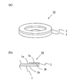
- (A) is a typical perspective view which shows the wavelength conversion member which concerns on the 1st Embodiment of this invention
- (b) is a figure which shows a part of side cross section of the wavelength conversion member of (a). It is a figure which shows a part of side cross section of the wavelength conversion member which concerns on the 2nd Embodiment of this invention. It is a figure which shows a part of side cross section of the wavelength conversion member which concerns on the 3rd Embodiment of this invention. It is a figure which shows a part of side cross section of the wavelength conversion member which concerns on the 4th Embodiment of this invention. It is a figure which shows a part of side cross section of the wavelength conversion member which concerns on the 5th Embodiment of this invention.
- (A) is a plan view of a wavelength conversion member according to a tenth embodiment of the present invention
- (b) is a cross-sectional view taken along line AA ′ of (a)
- (c) is a plan view of a heat dissipation layer in (a). It is. In an Example, it is a typical top view which shows the sample of the wavelength conversion member for performing characteristic evaluation.
- FIG. 1A is a schematic perspective view showing a wavelength conversion member according to the first embodiment of the present invention, and FIG. It is a figure which shows a part of side cross section of this wavelength conversion member.
- the wavelength converting member 10 includes a ring-shaped first porous ceramic layer 1 and a ring formed on the main surface thereof so that the outer diameter is substantially the same as that of the first porous ceramic layer 1 and is concentric. It has the wheel shape provided with the fluorescent substance layer 2 of a shape.
- the first porous ceramic layer 1 has a main surface 1a and a main surface 1b, and a phosphor layer 2 is formed on the main surface 1a.
- the excitation light is incident from the main surface 2a side of the phosphor layer 2, and is converted in wavelength by the phosphor contained in the phosphor layer 2 to emit fluorescence.
- the fluorescent light is reflected by the first porous ceramic layer 1 and irradiated to the outside from the main surface 2 a of the phosphor layer 2.
- the first porous ceramic layer 1 has a higher thermal conductivity than the phosphor layer 2, which facilitates efficient release of heat generated in the phosphor layer 2 to the outside.
- the porosity of the first porous ceramic layer 1 is 20% by volume or more, preferably 30% by volume or more, and particularly preferably 40% by volume or more. Since the first porous ceramic layer 1 has a porosity of 20% by volume or more, the first porous ceramic layer 1 exhibits a high light reflectance for the reasons described above.
- the upper limit of the porosity of the first porous ceramic layer 1 is preferably 80% by volume or less, 75% by volume or less, and particularly preferably 70% by volume or less. If the porosity of the first porous ceramic layer 1 is too high, the mechanical strength is lowered, or the heat conductivity is lowered to make it difficult to release the heat generated in the phosphor layer 2 to the outside.
- the first porous ceramic layer 1 is made of aluminum oxide, magnesium oxide, zirconium oxide, titanium oxide, niobium oxide, zinc oxide, silicon oxide, yttrium oxide, aluminum nitride, boron nitride, silicon nitride, silicon carbide, or the like. Can be mentioned. These may be used alone or in combination of two or more. Among these, aluminum oxide, magnesium oxide, and zirconium oxide are preferable because they have high thermal conductivity and are inexpensive. In particular, aluminum oxide is preferable. It is preferable that the material constituting the first porous ceramic layer 1 has a higher thermal conductivity than the phosphor layer 2.
- the first porous ceramic layer 1 preferably contains a readily sinterable ceramic powder. In this way, the bending strength of the first porous ceramic layer is improved, and as a result, the bending strength of the entire wavelength conversion member can also be improved.
- Easy-sinterable ceramic powder is a low-temperature sinterable ceramic powder.
- the sintering temperature of the easily sinterable ceramic powder is lowered by increasing the purity or decreasing the particle size.
- the easily sinterable ceramic powder can be sintered even when fired at a relatively low temperature of, for example, 1100 to 1550 ° C., further 1200 to 1400 ° C.
- the average particle size (D 50 ) of the easily sinterable ceramic powder is preferably 0.01 to 10 ⁇ m, particularly 0.05 to 5 ⁇ m, and particularly preferably 0.08 to 1 ⁇ m. By setting the average particle diameter within the above range, it becomes possible to sinter easily sinterable ceramic powder at a relatively low temperature.
- the purity of the easily sinterable ceramic powder is preferably 99% or more, 99.9% or more, and particularly preferably 99.99% or more.
- the easily sinterable ceramic powder can be sintered at a relatively low temperature.
- the easily sinterable ceramic powder examples include easily sinterable alumina powder and easily sinterable zirconia powder. Of these, easily sinterable alumina powder is preferred because of its excellent low-temperature sinterability.
- the easily sinterable alumina powder for example, AL-160SG series manufactured by Showa Denko KK, Tymicron TM-D series manufactured by Daimei Chemical Co., Ltd., or the like can be used.
- the content of the easily sinterable ceramic powder in the first porous ceramic layer is preferably 0.1 to 50%, 1 to 40%, particularly 5 to 30% by volume.
- the content of the easily sinterable ceramic powder is too small, the above effect is hardly obtained.
- there is too much content of an easily sinterable ceramic powder a porosity will fall and a light reflectance will fall easily.
- the thickness of the first porous ceramic layer 1 is preferably 0.05 to 2 mm, 0.1 to 1.5 mm, particularly preferably 0.2 to 1 mm.
- the thickness of the 1st porous ceramic layer 1 is too small, mechanical strength will fall and it will become easy to break at the time of use. Moreover, it becomes difficult to obtain sufficient light reflectance.
- the thickness of the 1st porous ceramic layer 1 is too large, there exists a tendency for the mass of the wavelength conversion member 10 and also the light emitting device using the same to become large. Further, when the wheel-shaped wavelength conversion member 10 is used as a light source for a projector, a load on a motor that rotates the wavelength conversion member 10 increases, or vibration due to rotation increases, which may cause damage.
- Examples of the phosphor layer 2 include those in which a phosphor is dispersed in an inorganic binder. Glass etc. are mentioned as an inorganic binder. Moreover, it becomes easy to match the thermal expansion coefficient with the first porous ceramic layer 1, and even when the temperature is raised by irradiation with excitation light, damage due to the difference in thermal expansion coefficient is less likely to occur.
- the glass used as the inorganic binder borosilicate glass, phosphate glass and the like can be used.
- the softening point of the glass is preferably 250 to 1000 ° C, particularly 300 to 850 ° C. If the softening point of the glass is too low, the mechanical strength of the phosphor layer 2 is lowered, or it is easily melted by irradiation with excitation light. On the other hand, if the softening point of the glass is too high, the phosphor is deteriorated in the firing step during production, and the light emission intensity of the phosphor layer 2 is likely to be lowered.
- the phosphor is not particularly limited as long as it emits fluorescence when incident excitation light is incident.
- Specific examples of the phosphor include, for example, an oxide phosphor, a nitride phosphor, an oxynitride phosphor, a chloride phosphor, an acid chloride phosphor, a sulfide phosphor, an oxysulfide phosphor, and a halide. Examples thereof include one or more selected from phosphors, chalcogenide phosphors, aluminate phosphors, halophosphate phosphors, and garnet compound phosphors.
- blue light is used as excitation light, for example, phosphors that emit green light, yellow light, or red light as fluorescence may be mixed and used.
- the average particle diameter (D 50 ) of the phosphor is preferably 1 to 50 ⁇ m, particularly preferably 5 to 25 ⁇ m. If the average particle size of the phosphor is too small, the emission intensity tends to decrease. On the other hand, if the average particle diameter of the phosphor is too large, the emission color tends to be non-uniform.
- the phosphor content in the phosphor layer 2 is preferably 5 to 80% by volume, 10 to 75% by volume, and particularly preferably 20 to 70% by volume. If the phosphor content is too small, the emission intensity tends to be insufficient. On the other hand, if the phosphor content is too large, the mechanical strength of the phosphor layer 2 tends to be insufficient.
- the thickness of the phosphor layer 2 is preferably thinner as long as the excitation light is surely absorbed by the phosphor. This is because if the phosphor layer 2 is too thick, the scattering and absorption of light in the phosphor layer 2 becomes too large, and the emission efficiency of fluorescence may be lowered.
- the thickness of the phosphor layer 2 is preferably 1 mm or less, 0.5 mm or less, particularly 0.3 mm or less.
- the lower limit of the thickness of the phosphor layer 2 is usually about 0.03 mm.
- the phosphor layer 2 is preferably bonded to the first porous ceramic layer 1 via a fused or inorganic bonding layer. If it does in this way, the heat resistance of the wavelength conversion member 10 can be improved. Further, the heat generated in the phosphor layer 2 can be efficiently dissipated to the first porous ceramic layer 1 side.
- the phosphor layer 2 is laminated on the main surface 1 a of the first porous ceramic layer 1, thermocompression bonded, and fired.
- a method is mentioned.
- the first porous ceramic layer 1 and the glass matrix in the phosphor layer 2 are fused.
- a transparent inorganic material by a sol-gel method is applied on the main surface 1a of the porous ceramic layer 1, and the phosphor is coated thereon.
- a method in which the layer 2 is laminated and heated is exemplified.
- the transparent inorganic material by the sol-gel method include polysilazane. Polysilazane reacts with moisture in the air to generate ammonia and condense, thereby forming a SiO 2 film.
- a bonding agent that forms an inorganic glass film at a relatively low temperature room temperature to 200 ° C.
- a bonding agent containing an alcohol-soluble organosilicon compound or other metal compound (organic or inorganic) and forming a SiO 2 network similar to glass at a relatively low temperature in the presence of a catalyst it can.
- a metal alkoxide is used as the organometallic compound and an alcohol is used as the catalyst, hydrolysis and dehydration are promoted, and as a result, a SiO 2 network is formed.
- the wavelength conversion member 10 can be manufactured as follows.
- a slurry containing ceramic powder as a raw material of the first porous ceramic layer 1 and an organic component such as a binder resin, a solvent, and a plasticizer is applied onto a resin film such as polyethylene terephthalate by a doctor blade method or the like, and heated. By drying, the 1st green sheet for porous ceramic layers 1 is produced.
- the average particle diameter (D 50 ) of the ceramic powder that is the raw material of the first porous ceramic layer 1 is preferably 0.1 to 10 ⁇ m. When the average particle diameter of the ceramic powder is too small, the porosity of the first porous ceramic layer 1 tends to be lowered.
- the first green sheet for porous ceramic layer 1 is fired at about 1200 to 1500 ° C. In this way, the first porous ceramic layer 1 is obtained.
- the firing temperature is too low, sintering tends to be insufficient.
- the firing temperature is too high, the porosity tends to decrease.
- a slurry containing glass powder as a glass matrix of the phosphor layer 2, phosphor and organic components such as a binder resin, a solvent, and a plasticizer is applied onto a resin film such as polyethylene terephthalate by a doctor blade method or the like. By heating and drying, a green sheet for the phosphor layer 2 is produced.
- the obtained porous ceramic layer 1 and the green sheet for the phosphor layer 2 are laminated and fired to obtain the wavelength conversion member 10 in which the porous ceramic layer 1 and the phosphor layer 2 are fusion bonded.
- the firing temperature is preferably within the range of the softening temperature of the glass powder in the phosphor layer 2 ⁇ 100 ° C., particularly within the range of the softening point of the glass powder ⁇ 50 ° C. If the firing temperature is too low, the phosphor layer 2 is difficult to fuse to the porous ceramic layer 1. Moreover, the sintering of the glass powder becomes insufficient, and the mechanical strength of the phosphor layer 2 tends to decrease. On the other hand, if the firing temperature is too high, the phosphor may deteriorate and the light emission intensity may decrease.
- the wavelength conversion member 10 is formed by fusion bonding the porous ceramic layer 1 and the phosphor layer 2 by applying and firing the slurry for the phosphor layer 2 on the surface of the porous ceramic layer 1. Can be obtained.
- the slurry for phosphor layer 2 used here the slurry used for producing the green sheet for phosphor layer 2 can be used.
- the porous ceramic layer 1 green sheet and the phosphor layer 2 green sheet are separately fired to obtain the porous ceramic layer 1 and the phosphor layer 2, they are bonded using an inorganic bonding agent. Accordingly, it is possible to obtain the wavelength conversion member 10 in which the porous ceramic layer 1 and the phosphor layer 2 are bonded by the inorganic bonding layer.
- a degreasing step for removing organic substances may be performed before firing the green sheet or slurry.
- the layers including the green sheet are stacked, the layers may be appropriately heat-pressed in order to enhance mutual adhesion.
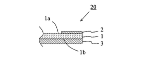
- FIG. 2 is a view showing a part of a side cross section of the wavelength conversion member according to the second embodiment of the present invention.
- the heat dissipation layer 3 is provided on the main surface 1b opposite to the main surface 1a on which the phosphor layer 2 of the porous ceramic layer 1 is formed. It differs from the wavelength conversion member 10 which concerns on 1 embodiment.
- the heat dissipation layer 3 has a ring shape whose outer diameter is substantially the same and concentric with the first porous ceramic layer 1. Other configurations are the same as those of the wavelength conversion member 10 according to the first embodiment.
- the heat conductivity of the heat radiation layer 3 is preferably 5 W / m ⁇ K or more, 10 W / m ⁇ K or more, and particularly preferably 20 W / m ⁇ K or more.
- Examples of the heat dissipation layer 3 include a dense ceramic layer.
- the porosity of the dense ceramic layer is less than 20% by volume, preferably 15% by volume or less, and particularly preferably 10% by volume or less. If the porosity of the dense ceramic layer is too high, the thermal conductivity is lowered, and the heat dissipation tends to be lowered.
- the lower limit of the porosity of the dense ceramic layer is not particularly limited, but is actually 0.2% by volume or more.
- the dense ceramic layer examples include those made of aluminum oxide, magnesium oxide, zirconium oxide, titanium oxide, niobium oxide, zinc oxide, yttrium oxide, aluminum nitride, boron nitride, silicon carbide and the like. These may be used alone or in combination of two or more. Among these, aluminum oxide, magnesium oxide, and zirconium oxide are preferable because they have high thermal conductivity and are inexpensive.
- the heat dissipation layer 3 may be made of a metal such as sapphire, aluminum, silver, or copper other than the above.
- the thickness of the heat dissipation layer 3 is preferably 0.2 to 2 mm, 0.3 to 1.5 mm, particularly preferably 0.5 to 1 mm.
- the thickness of the heat dissipation layer 3 is preferably 0.2 to 2 mm, 0.3 to 1.5 mm, particularly preferably 0.5 to 1 mm.
- the thickness of the heat dissipation layer 3 is too small, it is difficult to obtain a sufficient heat dissipation effect.
- the thickness of the heat dissipation layer 3 is too large, the wavelength conversion member 20 and the light emitting device using the wavelength conversion member 20 tend to increase in mass. Further, when the wheel-shaped wavelength conversion member 20 is used as a light source for a projector, a load on a motor that rotates the wavelength conversion member 20 increases, or vibration due to rotation increases, which may cause damage.
- the wavelength conversion member 20 can be manufactured as follows.
- the first green sheet for the porous ceramic layer 1 is produced in the same manner as in the wavelength conversion member 10.
- the heat dissipation layer 3 is prepared.
- a dense ceramic layer is used as the heat dissipation layer 3
- a green sheet for the dense ceramic layer is obtained in the same manner as the method for producing the green sheet for the porous ceramic layer 1 in the wavelength conversion member 10.
- a dense ceramic layer having a low porosity is obtained by sintering the green sheet for the dense ceramic layer at a relatively high temperature.
- the dense ceramic layer green sheet is fired at about 1500 ° C. or higher, preferably 1600 ° C. or higher.
- the average particle size of the ceramic powder which is a raw material (D 50) is small, easy to reduce the porosity of the dense ceramic layer.
- the first porous ceramic layer 1 green sheet and the heat dissipation layer 3 are stacked and fired to obtain a laminate in which the first porous ceramic layer 1 and the heat dissipation layer 3 are joined.
- the wavelength conversion member 20 is obtained by joining the phosphor layer 2 on the main surface 1a of the first porous ceramic layer 1 in the obtained laminate in the same manner as in the wavelength conversion member 10.
- the heat dissipation layer 3 may be bonded after the phosphor layer 2 is bonded to the first porous ceramic layer 1 first.
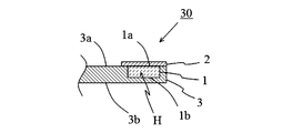
- FIG. 3 is a view showing a part of a side cross section of the wavelength conversion member according to the third embodiment of the present invention.
- the main surface 3a of the heat dissipation layer 3 is provided with a ring-shaped hole H that is concentric with the heat dissipation layer 3, and the porous ceramic layer 1 is provided in the hole H. It is different from the wavelength conversion member 20 according to the second embodiment in that it is formed.
- the phosphor layer 2 is provided on the main surface 1 a of the porous ceramic layer 1.
- the phosphor layer 2 is formed so as to cover the main surface 1 a of the porous ceramic layer 1, and a part of the phosphor layer 2 is formed on the main surface 3 a of the heat dissipation layer 3. .
- the wavelength conversion member 30 since a part of the phosphor layer 2 is formed on the heat dissipation layer 3, the heat generated in the phosphor layer 2 is more easily released to the outside.
- the wavelength conversion member 30 can be manufactured as follows.
- the heat dissipation layer 3 is prepared, and the hole H is formed in the main surface 3a of the heat dissipation layer 3 by cutting or the like.
- the hole H is formed on the main surface 3a by firing the green sheet for the dense ceramic layer in an appropriately laminated state so that the hole H is obtained. The formed heat dissipation layer 3 is obtained.
- the first green sheet for the porous ceramic layer 1 obtained in the same manner as in the wavelength conversion member 10 is cut in accordance with the shape of the hole H in the heat dissipation layer 3 and laminated in the hole H.
- the size of the first green sheet for the porous ceramic layer 1 is appropriately adjusted in consideration of shrinkage during firing (for example, it is made slightly larger than the size of the hole H).
- the 1st porous ceramic layer 1 is formed in the inside of the hole H of the thermal radiation layer 3 by baking.
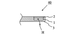
- FIG. 4 is a view showing a part of a side cross section of the wavelength conversion member according to the fourth embodiment of the present invention.
- the wavelength conversion member 40 according to the present embodiment is different from the wavelength conversion member 30 according to the third embodiment in that the phosphor layer 2 is formed inside the hole H. Specifically, the first porous ceramic layer 1 and the phosphor layer 2 are sequentially formed in the hole H formed in the main surface 3a of the wavelength conversion member 40.
- the heat generated in the phosphor layer 2 is more easily released to the outside.
- the wavelength conversion member 40 can be manufactured according to the method for manufacturing the wavelength conversion member 30.
- FIG. 5 is a view showing a part of a side cross section of the wavelength conversion member according to the fifth embodiment of the present invention.
- a ring-shaped notch C that is concentric with the heat dissipation layer 3 is formed on the main surface 3a of the heat dissipation layer 3, and a porous ceramic is formed in the notch C. It differs from the wavelength conversion member 30 according to the third embodiment in that the layer 1 is formed.
- the phosphor layer 2 is provided on the main surface 1 a of the porous ceramic layer 1.
- the phosphor layer 2 is formed so as to cover the main surface 1 a of the porous ceramic layer 1, and a part of the phosphor layer 2 is formed on the main surface 3 a of the heat dissipation layer 3. .
- a part of the phosphor layer 2 is formed on the heat dissipation layer 3. It becomes easier to release the generated heat to the outside.
- the wavelength conversion member 50 can be manufactured according to the manufacturing method of the wavelength conversion member 30.
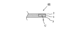
- FIG. 6 is a view showing a part of a side cross section of a wavelength conversion member according to the sixth embodiment of the present invention.
- the wavelength conversion member 60 according to the present embodiment relates to the fifth embodiment in that the phosphor layer 2 is formed inside a notch C provided on the main surface 3a of the heat dissipation layer 3. Different from the wavelength conversion member 50. Specifically, the first porous ceramic layer 1 and the phosphor layer 2 are sequentially formed in the notch C formed in the main surface 3 a of the wavelength conversion member 60.
- the heat generated in the phosphor layer 2 is more easily released to the outside.
- the wavelength conversion member 60 can be manufactured according to the method for manufacturing the wavelength conversion member 30.
- FIG. 7 is a view showing a part of a side cross section of the wavelength conversion member according to the seventh embodiment of the present invention.
- a second porous ceramic layer 1 ′ having substantially the same shape as the first porous ceramic layer 1 is provided on the main surface 3 b of the heat dissipation layer 3.
- Other configurations are the same as those of the wavelength conversion member 20 according to the second embodiment.
- the porosity and thickness range of the second porous ceramic layer 1 ′ and specific examples of the material the same materials as those of the first porous ceramic layer 1 can be selected. From the viewpoint of effectively suppressing the problem of warping of the wavelength conversion member 70 in the firing step during manufacturing, the porosity, thickness, and material of the first porous ceramic layer 1 and the second porous ceramic layer 1 ' It is preferable that at least one is the same, and it is more preferable that all of them are the same.
- the second porous ceramic layer 1 ′ preferably contains a readily sinterable ceramic powder.
- the bending strength of the second porous ceramic layer 1 ' can be improved, and as a result, the bending strength of the entire wavelength conversion member can also be improved.
- the content of the readily sinterable ceramic powder in the second porous ceramic layer 1 ′ is the first
- the content of the easily sinterable ceramic powder in the porous ceramic layer is preferably the same.
- the wavelength conversion member 70 can be manufactured as follows.
- the heat dissipation layer 3 is prepared in the same manner as in the wavelength conversion member 20. By laminating and firing the first porous ceramic layer 1 green sheet on the main surface 3a of the heat dissipation layer 3 and the second porous ceramic layer 1 ′ green sheet on the main surface 3b, each of the heat dissipation layers 3 is fired. A laminate is obtained in which the first porous ceramic layer 1 and the second porous ceramic layer 1 ′ are joined to the main surface.
- the wavelength conversion member 70 is obtained by bonding the phosphor layer 2 onto the main surface 1 a of the first porous ceramic layer 1 in the obtained laminate. .
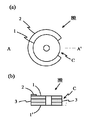
- FIG. 8A is a plan view of a wavelength conversion member 80 according to the eighth embodiment of the present invention, and FIG. -A 'sectional view.
- the wavelength conversion member 80 according to this embodiment is different from the wavelength conversion member 70 in that a notch C is provided in a part of the region where the phosphor layer 2 is formed.
- the configuration of each layer is the same as that of the wavelength conversion member 70.
- the notch C none of the phosphor layer 2, the first porous ceramic layer 1, the second porous ceramic layer 1 ′, and the heat dissipation layer 3 is formed, and a part of the outer periphery of the wheel is completely formed. The excitation light can be transmitted.
- the wavelength conversion member 80 it is possible to obtain a light emitting device that can appropriately use both the case where the excitation light is converted in wavelength by the phosphor layer 2 and the fluorescence is extracted and the case where the excitation light is extracted as it is. .
- FIG. 9A is a plan view of a wavelength conversion member 90 according to the ninth embodiment of the present invention, and FIG. -A 'sectional view.
- a notch C is provided in a part of the region where the phosphor layer 2 is formed.
- the phosphor layer 2 the first porous ceramic layer 1 and the second porous ceramic layer 1 ′ are not formed, and the main surfaces 3a and 3b of the heat dissipation layer 3 are exposed. This is different from the wavelength conversion member 80 in that.
- the excitation light can be transmitted through the notch C as in the wavelength conversion member 80.
- the wavelength conversion member 90 since the heat radiation layer 3 is formed in the cutout portion C, the mass balance of the entire member is excellent compared to the wavelength conversion member 80. Therefore, it is possible to suppress the occurrence of vibration and wind noise when the wavelength conversion member 90 is rotated at high speed. Furthermore, since the main surfaces 3a and 3b of the heat dissipation layer 3 are partially exposed, it is easy to dissipate the heat generated in the phosphor layer 2 to the outside.
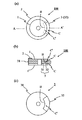
- FIG. 10A is a plan view of the wavelength conversion member 100 according to the tenth embodiment of the present invention
- FIG. 10B is an AA view of FIG. 'Cross sectional view
- (c) is a plan view of the heat dissipation layer 3.
- a notch C is provided in a part of the region where the phosphor layer 2 is formed, and the notch C has a phosphor layer. 2.
- the first porous ceramic layer 1 and the second porous ceramic layer 1 ′ are not formed, and the main surfaces 3a and 3b of the heat dissipation layer 3 are exposed.
- the heat radiation layer 3 used in the wavelength conversion member 100 is composed of heat radiation layer pieces 31 and 32.
- the heat dissipation layer piece 31 has a notch C ′
- the heat dissipation layer piece 32 having a shape corresponding to the notch C ′ is fitted into the notch C ′.
- the heat radiation layer pieces 31 and 32 may be joined by an adhesive at the boundary B.
- the boundary portion B of the heat dissipation layer pieces 31 and 32 in the heat dissipation layer 3 is formed in the first porous ceramic layer 1 and the second porous portion. While being covered with the ceramic layer 1 ′, only the heat radiation layer piece 32 is exposed in the notch C. Further, the heat radiation layer pieces 31 and 32 are fixed by being sandwiched between the first porous ceramic layer 1 and the second porous ceramic layer 1 ′ at the boundary portion B.
- the heat radiation layer piece 32 is made of a material that can transmit excitation light, such as sapphire, so that the excitation light can be transmitted through the cutout portion C as in the wavelength conversion member 90. Also in the wavelength conversion member 100, since the heat radiation layer 3 is formed in the notch C, it is possible to suppress the occurrence of vibration and wind noise when the wavelength conversion member 100 is rotated at high speed.
- the heat radiation layer piece 32 may be made of a material capable of transmitting excitation light, and the remaining heat radiation layer piece 31 has transmission characteristics with respect to excitation light. Is not questioned.
- sapphire is used as the heat dissipation layer piece 32
- aluminum oxide having a thermal expansion coefficient approximate to that of sapphire it is preferable to use aluminum oxide having a thermal expansion coefficient approximate to that of sapphire as the heat dissipation layer piece 31. If it does in this way, generation
- a light emitting device of the present invention includes the above-described wavelength conversion member (any one of the wavelength conversion members 10 to 70) and a light source that irradiates the wavelength conversion member with excitation light.
- a light source an LED, an LD, or the like can be used.
- the excitation light emitted from the light source is wavelength-converted by the phosphor layer in the wavelength conversion member to emit fluorescence, and the fluorescence is reflected by the first porous ceramic layer and emitted from the same side as the excitation light irradiation side. Is done.
- Table 1 shows examples and comparative examples of the present invention.
- Example 1 Preparation of green sheet for porous ceramic layer
- Al 2 O 3 powder average particle size (D 50 ): 1 ⁇ m
- polybutyl methacrylate as a binder
- methyl ethyl ketone as a plasticizer
- butyl benzyl phthalate as a solvent
- the obtained slurry was applied onto a polyethylene terephthalate (PET) film using a doctor blade method and dried to obtain a green sheet (thickness 0.32 mm) for a porous ceramic layer.
- PET polyethylene terephthalate
- the bending strength of the porous ceramic layer was measured as follows.
- the green sheet for a porous ceramic layer was degreased at 600 ° C. for 8 hours in the air, and further fired at 1400 ° C. for 5 hours to obtain a porous ceramic layer.
- the bending strength of the obtained porous ceramic layer was measured using a testing machine (AG-10kNIS manufactured by Shimadzu Corporation).
- the obtained glass powder and a YAG (Y 3 Al 5 O 12 ) phosphor powder were mixed with 30 vol% glass powder, YAG (Y 3 Al 5 O 12 ) phosphor.
- the powder was mixed to 70% by volume and mixed using a vibration mixer.
- a binder, a plasticizer, a solvent and the like were appropriately added to 50 g of the obtained mixed powder and kneaded for 24 hours to obtain a slurry.
- the obtained slurry was applied onto a PET film using a doctor blade method and dried to obtain a phosphor layer green sheet (thickness: 0.12 mm).
- a porous ceramic layer green sheet and a dense ceramic layer (Al 2 O 3 sheet, product name HA-96-2 manufactured by MARUWA, Inc .; thickness 0.8 mm, thermal conductivity 23 W / m ⁇ K) are stacked as a heat dissipation layer And applying a pressure of 10 MPa at 100 ° C. for 5 minutes using a thermocompression bonding machine to make them adhere closely, followed by degreasing treatment at 600 ° C. for 8 hours in the atmosphere, and further firing at 1400 ° C. for 5 hours As a result, a ceramic layer laminate composed of two layers of a porous ceramic layer and a dense ceramic layer was produced.
- the porosity of the porous ceramic layer and that of the dense ceramic layer were obtained by binarizing the cross-section reflected electron image and then calculating the area ratio of the pore portion.
- the light reflectance of the ceramic layer laminate was obtained from the average value of the reflected light intensity at each wavelength of 400 to 800 nm using UV-2500PC manufactured by Shimadzu Corporation.
- the green sheet for the phosphor layer was superposed on the porous ceramic layer of the ceramic layer laminate, and both were brought into close contact by applying a pressure of 10 MPa at 100 ° C. for 5 minutes using a thermocompression bonding machine. Thereafter, a degreasing treatment was performed in the air at 500 ° C. for 7 hours, and further, baking was performed at 700 ° C. for 1 hour to prepare a wavelength conversion member.
- Example 2 A green sheet for porous ceramic layer (thickness 0.26 mm) was produced in the same manner as in Example 1. After four layers of porous ceramic layer green sheets are stacked and adhered by applying a pressure of 10 MPa at 100 ° C. for 5 minutes using a thermocompression bonding machine, degreasing treatment is performed at 600 ° C. for 8 hours in the atmosphere. The porous ceramic layer was obtained by baking at 1400 degreeC for 5 hours. The light reflectance of the porous ceramic layer was measured in the same manner as in Example 1. The results are shown in Table 1.
- the porous ceramic layer and the phosphor layer green sheet obtained in Example 1 were superposed and adhered by applying a pressure of 10 MPa at 100 ° C. for 5 minutes using a thermocompression bonding machine, and then in the atmosphere.
- the wavelength conversion member was produced by performing a degreasing process at 500 degreeC for 7 hours, and also baking at 700 degreeC for 1 hour.
- Example 3 Bonded to a mixed powder of 90% by volume of Al 2 O 3 powder (average particle size (D 50 ): 1 ⁇ m) and 10% by volume of readily sinterable alumina powder (Taimicron TM-D manufactured by Daimei Chemical Co., Ltd.) Polybutyl methacrylate as an agent, methyl ethyl ketone as a plasticizer, and butylbenzyl phthalate as a solvent were appropriately added, and kneaded for 24 hours to obtain a slurry. The obtained slurry was applied onto a polyethylene terephthalate (PET) film using a doctor blade method and dried to obtain a green sheet (thickness 0.32 mm) for a porous ceramic layer.
- PET polyethylene terephthalate
- a wavelength conversion member was produced in the same manner as in Example 1 except that the obtained green sheet for porous ceramic layer was used.
- Example 4 Wavelength conversion was performed in the same manner as in Example 3 except that a mixed powder of 80% by volume of Al 2 O 3 powder and 20% by volume of readily sinterable alumina powder was used when producing a green sheet for a porous ceramic layer. A member was prepared.
- Example 1 Using the thermocompression bonding machine, the green sheet for the phosphor layer obtained in Example 1 was applied to a dense ceramic layer (Al 2 O 3 sheet manufactured by MARUWA, Inc., product name HA-96-2; thickness 0.635 mm). After making it adhere by applying a pressure of 10 MPa at 100 ° C. for 5 minutes, a degreasing treatment was performed in the atmosphere at 500 ° C. for 7 hours, and further baking at 700 ° C. for 1 hour to obtain a wavelength conversion member. The light reflectance of the dense ceramic layer was measured in the same manner as in Example 1. The results are shown in Table 1.
- the surface of the phosphor layer of the wavelength conversion member rotated at 8000 rpm was irradiated with a laser beam with an output of 30 W from a blue laser light source having a wavelength of 440 nm.
- the obtained fluorescence was received by a small spectroscope (USB-4000, manufactured by Ocean Optics) through an optical fiber, and an emission spectrum was obtained.
- the fluorescence peak intensity was read from the emission spectrum.
- the surface temperature of the phosphor layer was measured using a thermography i5 manufactured by FLIR.
- the wavelength conversion members of Examples 1 to 4 had a fluorescence peak intensity of 1251 (au) or higher, whereas the wavelength conversion member of the comparative example had a fluorescence peak intensity of 1098 ( a.u.) and inferior.
- Example 1 and Example 2 when a laminated body of a porous ceramic layer and a dense ceramic layer is used as the light reflecting layer, it can be seen that the light reflectance is improved. Further, when a dense ceramic layer is laminated on the porous ceramic layer, the temperature of the phosphor layer is also lowered, which is considered to reduce the temperature quenching of the phosphor.
- the wavelength conversion member of Example 1 is considered to have a higher fluorescence peak intensity than the wavelength conversion member of Example 2. Furthermore, when Examples 1, 3, and 4 are compared, it can be seen that the bending strength is improved by adding easily sinterable alumina to the porous ceramic layer.
Landscapes
- Physics & Mathematics (AREA)
- Engineering & Computer Science (AREA)
- Chemical & Material Sciences (AREA)
- General Physics & Mathematics (AREA)
- Spectroscopy & Molecular Physics (AREA)
- Multimedia (AREA)
- General Engineering & Computer Science (AREA)
- Ceramic Engineering (AREA)
- Optics & Photonics (AREA)
- Signal Processing (AREA)
- Structural Engineering (AREA)
- Organic Chemistry (AREA)
- Materials Engineering (AREA)
- Inorganic Chemistry (AREA)
- Astronomy & Astrophysics (AREA)
- Optical Filters (AREA)
- Led Device Packages (AREA)
- Ceramic Products (AREA)
- Projection Apparatus (AREA)
- Porous Artificial Stone Or Porous Ceramic Products (AREA)
- Luminescent Compositions (AREA)
- Non-Portable Lighting Devices Or Systems Thereof (AREA)
- Manufacturing & Machinery (AREA)
Abstract
Description
図1の(a)は、本発明の第1の実施形態に係る波長変換部材を示す模式的斜視図であり、(b)は(a)の波長変換部材の側断面の一部を示す図である。
図2は、本発明の第2の実施形態に係る波長変換部材の側断面の一部を示す図である。本実施形態に係る波長変換部材20では、多孔質セラミック層1の蛍光体層2が形成された主面1aとは反対側の主面1b上に放熱層3が設けられている点で、第1の実施形態に係る波長変換部材10と異なる。放熱層3は、第1の多孔質セラミック層1と外径が略同一かつ同心であるリング状である。その他の構成は第1の実施形態に係る波長変換部材10と同じである。多孔質セラミック層1の主面1b上に放熱層3を設けることにより、既述の理由から、蛍光体層2で発生し、第1のセラミック層1に伝導した熱が放熱層3を通じて外部に放出されやすくなる。放熱層3の熱伝導率は5W/m・K以上、10W/m・K以上、特に20W/m・K以上であることが好ましい。
図3は、本発明の第3の実施形態に係る波長変換部材の側断面の一部を示す図である。本実施形態に係る波長変換部材30では、放熱層3の主面3aに、放熱層3と同心であるリング状の穴部Hが設けられており、穴部H内に多孔質セラミック層1が形成されている点で、第2の実施形態に係る波長変換部材20と異なる。蛍光体層2は多孔質セラミック層1の主面1a上に設けられている。具体的には、蛍光体層2は多孔質セラミック層1の主面1aを覆うように形成されており、かつ蛍光体層2の一部は放熱層3の主面3a上に形成されている。本実施形態に係る波長変換部材30では、蛍光体層2の一部が放熱層3上に形成されているため、蛍光体層2で発生した熱をより一層外部に放出しやすくなる。
(4)第4の実施形態に係る波長変換部材
図4は、本発明の第4の実施形態に係る波長変換部材の側断面の一部を示す図である。本実施形態に係る波長変換部材40では、蛍光体層2が穴部Hの内部に形成されている点で、第3の実施形態に係る波長変換部材30とは異なる。具体的には、波長変換部材40の主面3aに形成された穴部Hの内部に、第1の多孔質セラミック層1及び蛍光体層2が順に形成されている。
図5は、本発明の第5の実施形態に係る波長変換部材の側断面の一部を示す図である。本実施形態に係る波長変換部材50では、放熱層3の主面3a上に、放熱層3と同心であるリング状の切り欠き部Cが形成されており、切り欠き部C内に多孔質セラミック層1が形成されている点で、第3の実施形態に係る波長変換部材30と異なる。蛍光体層2は多孔質セラミック層1の主面1a上に設けられている。具体的には、蛍光体層2は多孔質セラミック層1の主面1aを覆うように形成されており、かつ蛍光体層2の一部は放熱層3の主面3a上に形成されている。第3の実施形態に係る波長変換部材30と同様に、本実施形態に係る波長変換部材50では、蛍光体層2の一部が放熱層3上に形成されているため、蛍光体層2で発生した熱をより一層外部に放出しやすくなる。
図6は、本発明の第6の実施形態に係る波長変換部材の側断面の一部を示す図である。本実施形態に係る波長変換部材60では、蛍光体層2が、放熱層3の主面3a上に設けられた切り欠き部Cの内部に形成されている点で、第5の実施形態に係る波長変換部材50とは異なる。具体的には、波長変換部材60の主面3aに形成された切り欠き部Cの内部に、第1の多孔質セラミック層1及び蛍光体層2が順に形成されている。
図7は、本発明の第7の実施形態に係る波長変換部材の側断面の一部を示す図である。本実施形態に係る波長変換部材70では、放熱層3の主面3b上に、第1の多孔質セラミック層1と略同一形状の第2の多孔質セラミック層1’が設けられている。その他の構成は第2の実施形態に係る波長変換部材20と同じである。
図8の(a)は、本発明の第8の実施形態に係る波長変換部材80の平面図であり、(b)は(a)のA-A’断面図である。本実施形態に係る波長変換部材80では、蛍光体層2が形成されている領域の一部において切り欠き部Cが設けられている点で波長変換部材70と異なっている。各層の構成は波長変換部材70と同じである。切り欠き部Cにおいては、蛍光体層2、第1の多孔質セラミック層1、第2の多孔質セラミック層1’及び放熱層3のいずれも形成されておらず、ホイール外周の一部が完全に欠損した形態となっており、励起光が透過できるようになっている。よって、波長変換部材80を用いることにより、励起光を蛍光体層2で波長変換させて蛍光を取り出す場合と、励起光をそのまま取り出す場合の両者を適宜使い分けることができる発光デバイスを得ることができる。
図9の(a)は、本発明の第9の実施形態に係る波長変換部材90の平面図であり、(b)は(a)のA-A’断面図である。波長変換部材90では、蛍光体層2が形成されている領域の一部において切り欠き部Cが設けられている。切り欠き部Cにおいては、蛍光体層2、第1の多孔質セラミック層1及び第2の多孔質セラミック層1’が形成されておらず、放熱層3の主面3a及び3bが露出した状態となっている点で波長変換部材80と異なる。ここで、サファイア等の励起光を透過可能な材料で放熱層3を構成することにより、波長変換部材80と同様に、切り欠き部Cにおいて励起光を透過させることが可能となる。なお、波長変換部材90では、切り欠き部Cにおいて放熱層3が形成されているため、波長変換部材80と比較して、部材全体の質量バランスに優れている。よって、波長変換部材90を高速で回転させた場合の振動や風切り音の発生を抑制することができる。さらに、放熱層3の主面3a及び3bが一部露出しているため、蛍光体層2で発生した熱を外部に放熱させやすい。
図10の(a)は、本発明の第10の実施形態に係る波長変換部材100の平面図、(b)は(a)のA-A’断面図、(c)は放熱層3の平面図である。波長変換部材100では、波長変換部材90と同様に、蛍光体層2が形成されている領域の一部において切り欠き部Cが設けられており、かつ、切り欠き部Cにおいては、蛍光体層2、第1の多孔質セラミック層1及び第2の多孔質セラミック層1’が形成されておらず、放熱層3の主面3a、3bが露出した状態となっている。
本発明の発光デバイスは、上記の波長変換部材(波長変換部材10~70のいずれか)と、波長変換部材に励起光を照射する光源とを備えてなる。光源としてはLEDやLD等を使用することができる。光源から照射された励起光は波長変換部材における蛍光体層で波長変換されて蛍光を発し、当該蛍光は第1の多孔質セラミック層で反射されて、励起光照射側と同じ側から蛍光が出射される。

(多孔質セラミック層用グリーンシートの作製)
Al2O3粉末(平均粒子径(D50):1μm)に対して、結合剤としてポリブチルメタクリレート、可塑剤としてメチルエチルケトン、溶剤としてブチルベンジルフタレートを適宜添加し、24時間混練することによりスラリーを得た。得られたスラリーをドクターブレード法を用いてポリエチレンテレフタレート(PET)フィルム上に塗布し、乾燥させることにより、多孔質セラミック層用グリーンシート(厚み0.32mm)を得た。
モル%で、SiO2:58%、Al2O3:6%、B2O3:17%、Li2O:8%、Na2O:8%、K2O:3%のガラス組成となるよう原料を調合し、溶融急冷法によってフィルム状ガラスを得た。得られたフィルム状ガラスをボールミルを用いて粉砕し、平均粒子径(D50)が1μmのガラス粉末を得た。
多孔質セラミック層用グリーンシートと、放熱層として緻密質セラミック層(株式会社MARUWA製Al2O3シート 製品名HA-96-2;厚み0.8mm、熱伝導率23W/m・K)を重ね合わせ、熱圧着機を用いて、100℃で5分、10MPaの圧力を印加して両者を密着させた後、大気中にて600℃で8時間脱脂処理を行い、さらに1400℃で5時間焼成することにより、多孔質セラミック層と緻密質セラミック層の2層からなるセラミック層積層体を作製した。
実施例1と同様にして多孔質セラミック層用グリーンシート(厚み0.26mm)を作製した。多孔質セラミック層用グリーンシートを4層重ねて熱圧着機を用いて100℃で5分、10MPaの圧力を印可することにより密着させた後、大気中にて600℃で8時間脱脂処理を行い、1400℃で5時間焼成することにより多孔質セラミック層を得た。多孔質セラミック層の光反射率を実施例1と同様にして測定した。結果を表1に示す。
Al2O3粉末(平均粒子径(D50):1μm)90体積%と易焼結性アルミナ粉末(大明化学工業株式会社製タイミクロンTM-D)10体積%の混合粉末に対して、結合剤としてポリブチルメタクリレート、可塑剤としてメチルエチルケトン、溶剤としてブチルベンジルフタレートを適宜添加し、24時間混練することによりスラリーを得た。得られたスラリーをドクターブレード法を用いてポリエチレンテレフタレート(PET)フィルム上に塗布し、乾燥させることにより、多孔質セラミック層用グリーンシート(厚み0.32mm)を得た。
多孔質セラミック層用グリーンシートを作製する際に、Al2O3粉末80体積%と易焼結性アルミナ粉末20体積%の混合粉末を用いたこと以外は、実施例3と同様にして波長変換部材を作製した。
実施例1で得られた蛍光体層用グリーンシートを、緻密質セラミック層(株式会社MARUWA製Al2O3シート 製品名HA-96-2;厚み0.635mm)に熱圧着機を用いて、100℃で5分、10MPaの圧力を印加することにより密着させた後、大気中にて500℃で7時間脱脂処理を行い、さらに700℃で1時間焼成することにより波長変換部材を得た。なお、緻密質セラミック層の光反射率を実施例1と同様にして測定した。結果を表1に示す。
上記のようにして作製した各波長変換部材につき、蛍光ピーク強度と、蛍光体層の表面温度を下記のようにして測定した。結果を表1に示す。なお、測定には図11に示すサイズのもの(各層の厚みは表1に示す通り)を用いた。
1’ 第2の多孔質セラミック層
2 蛍光体層
3 放熱層
10、20、30、40、50、60、70、80、90、100 波長変換部材
31、32 放熱層片
H 穴部
C、C’ 切り欠き部
B 境界部
Claims (14)
- 気孔率が20体積%以上の第1の多孔質セラミック層と、第1の多孔質セラミック層の主面に形成される蛍光体層とを備えることを特徴とする波長変換部材。
- 蛍光体層が、第1の多孔質セラミック層に融着または無機接合層を介して接合していることを特徴とする請求項1に記載の波長変換部材。
- 第1の多孔質セラミック層が、酸化アルミニウム、酸化マグネシウム及び酸化ジルコニウムから選択される少なくとも1種からなることを特徴とする請求項1または2に記載の波長変換部材。
- 第1の多孔質セラミック層の、蛍光体層が形成された主面とは反対側の主面に、放熱層が形成されていることを特徴とする請求項1~3のいずれか一項に記載の波長変換部材。
- 放熱層が、気孔率が20体積%未満の緻密質セラミック層であることを特徴とする請求項1~4のいずれか一項に記載の波長変換部材。
- 緻密質セラミック層が、酸化アルミニウム、酸化マグネシウム及び酸化ジルコニウムから選択される少なくとも1種からなることを特徴とする請求項5に記載の波長変換部材。
- 放熱層の、第1の多孔質セラミック層が形成された主面とは反対側の主面に、気孔率20体積%以上の第2の多孔質セラミック層が形成されていることを特徴とする請求項4~6のいずれか一項に記載の波長変換部材。
- 第1の多孔質セラミック層と第2の多孔質セラミック層の気孔率、厚み及び/または材質が同一であることを特徴とする請求項7に記載の波長変換部材。
- 第1の多孔質セラミック層及び/または第2の多孔質セラミック層が易焼結性セラミック粉末を含有することを特徴とする請求項1~8のいずれか一項に記載の波長変換部材。
- 第1の多孔質セラミック層及び/または第2の多孔質セラミック層における易焼結性セラミック粉末の含有量が、体積%で0.1~50%であることを特徴とする請求項9に記載の波長変換部材。
- 蛍光体層が、無機バインダー中に蛍光体が分散してなることを特徴とする請求項1~10のいずれか一項に記載の波長変換部材。
- ホイール形状であることを特徴とする請求項1~11のいずれか一項に記載の波長変換部材。
- 請求項1~12のいずれか一項に記載の波長変換部材と、
波長変換部材における蛍光体層に励起光を照射する光源とを備えることを特徴とする発光デバイス。 - プロジェクター光源として使用されることを特徴とする請求項13に記載の発光デバイス。
Priority Applications (4)
| Application Number | Priority Date | Filing Date | Title |
|---|---|---|---|
| US15/539,724 US10557614B2 (en) | 2015-02-03 | 2016-01-22 | Projector light source including wavelength conversion member having porous ceramic substrate |
| CN201680008593.3A CN107209302A (zh) | 2015-02-03 | 2016-01-22 | 波长转换部件及使用其的发光装置 |
| JP2016573282A JPWO2016125611A1 (ja) | 2015-02-03 | 2016-01-22 | 波長変換部材及びそれを用いた発光デバイス |
| KR1020177015810A KR20170113533A (ko) | 2015-02-03 | 2016-01-22 | 파장 변환 부재 및 그것을 사용한 발광 디바이스 |
Applications Claiming Priority (4)
| Application Number | Priority Date | Filing Date | Title |
|---|---|---|---|
| JP2015018967 | 2015-02-03 | ||
| JP2015-018967 | 2015-02-03 | ||
| JP2015-060499 | 2015-03-24 | ||
| JP2015060499 | 2015-03-24 |
Publications (1)
| Publication Number | Publication Date |
|---|---|
| WO2016125611A1 true WO2016125611A1 (ja) | 2016-08-11 |
Family
ID=56563962
Family Applications (1)
| Application Number | Title | Priority Date | Filing Date |
|---|---|---|---|
| PCT/JP2016/051903 Ceased WO2016125611A1 (ja) | 2015-02-03 | 2016-01-22 | 波長変換部材及びそれを用いた発光デバイス |
Country Status (6)
| Country | Link |
|---|---|
| US (1) | US10557614B2 (ja) |
| JP (2) | JPWO2016125611A1 (ja) |
| KR (1) | KR20170113533A (ja) |
| CN (1) | CN107209302A (ja) |
| TW (1) | TWI673252B (ja) |
| WO (1) | WO2016125611A1 (ja) |
Cited By (18)
| Publication number | Priority date | Publication date | Assignee | Title |
|---|---|---|---|---|
| WO2018056157A1 (ja) * | 2016-09-21 | 2018-03-29 | パナソニックIpマネジメント株式会社 | 波長変換装置及び照明装置 |
| WO2018083903A1 (ja) * | 2016-11-02 | 2018-05-11 | 日本電気硝子株式会社 | 波長変換部材、発光デバイス及び波長変換部材の製造方法 |
| CN108105604A (zh) * | 2016-11-25 | 2018-06-01 | 深圳市光峰光电技术有限公司 | 发光陶瓷结构及其制备方法、相关发光装置和投影装置 |
| WO2018171083A1 (zh) * | 2017-03-21 | 2018-09-27 | 深圳市光峰光电技术有限公司 | 光源装置及色轮 |
| JP2018163947A (ja) * | 2017-03-24 | 2018-10-18 | 日本電気硝子株式会社 | 波長変換部材及び発光デバイス |
| WO2018230333A1 (ja) * | 2017-06-14 | 2018-12-20 | 日本電気硝子株式会社 | 波長変換部材及び発光デバイス |
| JP2018205599A (ja) * | 2017-06-07 | 2018-12-27 | セイコーエプソン株式会社 | 波長変換素子、波長変換装置、光源装置およびプロジェクター |
| EP3447577A1 (en) * | 2017-08-22 | 2019-02-27 | Seiko Epson Corporation | Wavelength converter, light source apparatus, and projector |
| JP2019039992A (ja) * | 2017-08-23 | 2019-03-14 | 日本特殊陶業株式会社 | 蛍光体ホイール、ホイールデバイスおよびプロジェクター |
| WO2019069871A1 (ja) * | 2017-10-02 | 2019-04-11 | 株式会社小糸製作所 | 波長変換部材および光源モジュール |
| WO2019131730A1 (ja) * | 2017-12-27 | 2019-07-04 | 京セラ株式会社 | カラーホイール、およびプロジェクタ |
| CN110579933A (zh) * | 2018-06-11 | 2019-12-17 | 中强光电股份有限公司 | 波长转换元件、投影装置及波长转换元件的制作方法 |
| JP2020154033A (ja) * | 2019-03-18 | 2020-09-24 | セイコーエプソン株式会社 | 波長変換素子、光源装置、プロジェクター、及び波長変換素子の製造方法 |
| WO2021145252A1 (ja) * | 2020-01-17 | 2021-07-22 | ソニーグループ株式会社 | 波長変換素子および光源モジュールならびに投射型表示装置 |
| EP3958057A1 (en) * | 2020-08-20 | 2022-02-23 | Delta Electronics, Inc. | Wavelength conversion member and light source module |
| US11387391B2 (en) | 2017-02-28 | 2022-07-12 | Osram Gmbh | Conversion element, optoelectronic component and method for producing a conversion element |
| US11500278B2 (en) | 2018-06-11 | 2022-11-15 | Coretronic Corporation | Wavelength-converting element, projection apparatus, and manufacturing method of wavelength-converting element |
| JP7296951B2 (ja) | 2017-09-20 | 2023-06-23 | マテリオン プレシジョン オプティクス (シャンハイ) リミテッド | 改良された無機結合剤を伴う光変換デバイス |
Families Citing this family (15)
| Publication number | Priority date | Publication date | Assignee | Title |
|---|---|---|---|---|
| KR102488528B1 (ko) * | 2017-09-20 | 2023-01-17 | 마테리온 프레시젼 옵틱스 (상하이) 리미티드 | 무기질 바인더를 갖는 인광체 휠 |
| CN109696792B (zh) | 2017-10-24 | 2022-03-29 | 中强光电股份有限公司 | 投影机及波长转换装置 |
| CN111699420B (zh) * | 2018-02-14 | 2023-01-13 | 日本特殊陶业株式会社 | 光波长转换装置 |
| CN112585534B (zh) * | 2018-08-27 | 2022-10-04 | 索尼公司 | 波长转换元件、光源模块及投影显示装置 |
| WO2020161963A1 (ja) * | 2019-02-04 | 2020-08-13 | パナソニックIpマネジメント株式会社 | 波長変換部材及びプロジェクタ |
| JP6922939B2 (ja) * | 2019-03-18 | 2021-08-18 | セイコーエプソン株式会社 | 波長変換素子、光源装置、プロジェクター、及び波長変換素子の製造方法 |
| CN110262173A (zh) * | 2019-05-31 | 2019-09-20 | 苏州佳世达光电有限公司 | 易散热的荧光色轮及投影机 |
| CN112578552A (zh) | 2019-09-30 | 2021-03-30 | 台达电子工业股份有限公司 | 波长转换装置 |
| CN112578551A (zh) | 2019-09-30 | 2021-03-30 | 台达电子工业股份有限公司 | 波长转换装置 |
| CN115004104A (zh) * | 2020-01-22 | 2022-09-02 | 索尼集团公司 | 光学元件、光源装置和投影仪 |
| US12546989B2 (en) | 2020-06-30 | 2026-02-10 | Lg Electronics Inc. | Phosphor wheel, illuminator, and projector |
| TWI845746B (zh) * | 2020-08-20 | 2024-06-21 | 台達電子工業股份有限公司 | 波長轉換元件及光源模組 |
| CN114815477B (zh) * | 2021-01-20 | 2024-10-18 | 中强光电股份有限公司 | 波长转换模块以及投影机 |
| CN113603462B (zh) * | 2021-07-20 | 2022-08-26 | 中国计量大学 | 一种陶瓷-玻璃复合结构荧光色轮及其制备方法和在激光显示源中的应用 |
| CN116165834A (zh) * | 2021-11-24 | 2023-05-26 | 中强光电股份有限公司 | 波长转换元件及投影机 |
Citations (9)
| Publication number | Priority date | Publication date | Assignee | Title |
|---|---|---|---|---|
| JP2003297551A (ja) * | 2002-03-29 | 2003-10-17 | Pioneer Electronic Corp | 有機エレクトロルミネッセンス表示パネル |
| JP2006287132A (ja) * | 2005-04-04 | 2006-10-19 | Kyoritsu Elex Co Ltd | 発光ダイオード用パッケージ及び発光ダイオード |
| JP2011191785A (ja) * | 2005-03-29 | 2011-09-29 | Kyocera Corp | 反射部材、これを用いた発光装置および照明装置 |
| JP2012227363A (ja) * | 2011-04-20 | 2012-11-15 | Kyocera Corp | 発光装置 |
| JP2012227224A (ja) * | 2011-04-15 | 2012-11-15 | Kyocera Corp | 発光装置 |
| JP2013207049A (ja) * | 2012-03-28 | 2013-10-07 | Nec Corp | 波長変換体を用いた発光装置 |
| JP2013247067A (ja) * | 2012-05-29 | 2013-12-09 | Nichia Chem Ind Ltd | 色変換用無機成形体及びその製造方法、並びに発光装置 |
| JP2014119492A (ja) * | 2012-12-13 | 2014-06-30 | Nippon Electric Glass Co Ltd | プロジェクタ用カラーホイール及びプロジェクタ用発光デバイス |
| JP2014229503A (ja) * | 2013-05-23 | 2014-12-08 | パナソニック株式会社 | 発光素子とその製造方法、およびプロジェクター |
Family Cites Families (19)
| Publication number | Priority date | Publication date | Assignee | Title |
|---|---|---|---|---|
| CN1643989A (zh) * | 2002-03-29 | 2005-07-20 | 先锋株式会社 | 有机电致发光显示面板 |
| WO2007141688A1 (en) * | 2006-06-02 | 2007-12-13 | Philips Intellectual Property & Standards Gmbh | Colored and white light generating lighting device |
| CN103777302A (zh) * | 2007-09-27 | 2014-05-07 | 欧瑞康贸易股份公司(特吕巴赫) | 色轮制造方法 |
| US8684560B2 (en) * | 2009-11-18 | 2014-04-01 | Stanley Electric Co., Ltd. | Semiconductor light source apparatus and lighting unit |
| US8556437B2 (en) * | 2009-12-17 | 2013-10-15 | Stanley Electric Co., Ltd. | Semiconductor light source apparatus and lighting unit |
| EP2595750A2 (en) * | 2010-07-22 | 2013-05-29 | Green Bubble Technologies LLC | Biooptical and biofunctional properties, applications and methods of polylactic acid films |
| JP2012243624A (ja) * | 2011-05-20 | 2012-12-10 | Stanley Electric Co Ltd | 光源装置および照明装置 |
| US20130088689A1 (en) * | 2011-10-07 | 2013-04-11 | Young Optics Inc. | Light source module and projection apparatus |
| DE102011084961A1 (de) * | 2011-10-21 | 2013-04-25 | Osram Gmbh | Leuchtstoffrad, Verfahren zum Herstellen eines Leuchtstoffrads und Beleuchtungsanordnung |
| CN103367611B (zh) | 2012-03-28 | 2017-08-08 | 日亚化学工业株式会社 | 波长变换用无机成型体及其制造方法以及发光装置 |
| JP2013214629A (ja) * | 2012-04-03 | 2013-10-17 | Nippon Electric Glass Co Ltd | 波長変換部材及び発光デバイス |
| JP6305009B2 (ja) * | 2013-01-11 | 2018-04-04 | 三菱電機株式会社 | 光源装置およびプロジェクタ |
| CN106195924B (zh) * | 2013-06-08 | 2019-05-03 | 深圳光峰科技股份有限公司 | 一种波长转换装置及其制作方法、相关发光装置 |
| JP6136617B2 (ja) | 2013-06-18 | 2017-05-31 | 日亜化学工業株式会社 | 光源装置及びプロジェクタ |
| CN203489181U (zh) * | 2013-10-15 | 2014-03-19 | 深圳市光峰光电技术有限公司 | 色轮及其光源系统、投影系统 |
| CN104566230B (zh) * | 2013-10-15 | 2017-07-11 | 深圳市光峰光电技术有限公司 | 波长转换装置及其光源系统、投影系统 |
| CN104566229B (zh) * | 2013-10-15 | 2016-06-08 | 深圳市光峰光电技术有限公司 | 波长转换装置的制造方法 |
| US20150153487A1 (en) * | 2013-11-29 | 2015-06-04 | Delta Electronics, Inc. | Wavelength-converting device |
| TWI579589B (zh) * | 2015-08-31 | 2017-04-21 | 中強光電股份有限公司 | 波長轉換裝置及投影機 |
-
2016
- 2016-01-22 US US15/539,724 patent/US10557614B2/en active Active
- 2016-01-22 CN CN201680008593.3A patent/CN107209302A/zh active Pending
- 2016-01-22 JP JP2016573282A patent/JPWO2016125611A1/ja active Pending
- 2016-01-22 WO PCT/JP2016/051903 patent/WO2016125611A1/ja not_active Ceased
- 2016-01-22 KR KR1020177015810A patent/KR20170113533A/ko not_active Withdrawn
- 2016-01-27 TW TW105102552A patent/TWI673252B/zh active
-
2020
- 2020-07-15 JP JP2020121351A patent/JP6879417B2/ja active Active
Patent Citations (9)
| Publication number | Priority date | Publication date | Assignee | Title |
|---|---|---|---|---|
| JP2003297551A (ja) * | 2002-03-29 | 2003-10-17 | Pioneer Electronic Corp | 有機エレクトロルミネッセンス表示パネル |
| JP2011191785A (ja) * | 2005-03-29 | 2011-09-29 | Kyocera Corp | 反射部材、これを用いた発光装置および照明装置 |
| JP2006287132A (ja) * | 2005-04-04 | 2006-10-19 | Kyoritsu Elex Co Ltd | 発光ダイオード用パッケージ及び発光ダイオード |
| JP2012227224A (ja) * | 2011-04-15 | 2012-11-15 | Kyocera Corp | 発光装置 |
| JP2012227363A (ja) * | 2011-04-20 | 2012-11-15 | Kyocera Corp | 発光装置 |
| JP2013207049A (ja) * | 2012-03-28 | 2013-10-07 | Nec Corp | 波長変換体を用いた発光装置 |
| JP2013247067A (ja) * | 2012-05-29 | 2013-12-09 | Nichia Chem Ind Ltd | 色変換用無機成形体及びその製造方法、並びに発光装置 |
| JP2014119492A (ja) * | 2012-12-13 | 2014-06-30 | Nippon Electric Glass Co Ltd | プロジェクタ用カラーホイール及びプロジェクタ用発光デバイス |
| JP2014229503A (ja) * | 2013-05-23 | 2014-12-08 | パナソニック株式会社 | 発光素子とその製造方法、およびプロジェクター |
Cited By (40)
| Publication number | Priority date | Publication date | Assignee | Title |
|---|---|---|---|---|
| JP2020030414A (ja) * | 2016-09-21 | 2020-02-27 | パナソニックIpマネジメント株式会社 | 波長変換装置及び照明装置 |
| JP2020030413A (ja) * | 2016-09-21 | 2020-02-27 | パナソニックIpマネジメント株式会社 | 波長変換装置及び照明装置 |
| JP2020076971A (ja) * | 2016-09-21 | 2020-05-21 | パナソニックIpマネジメント株式会社 | 波長変換装置及び照明装置 |
| JPWO2018056157A1 (ja) * | 2016-09-21 | 2019-02-21 | パナソニックIpマネジメント株式会社 | 波長変換装置及び照明装置 |
| WO2018056157A1 (ja) * | 2016-09-21 | 2018-03-29 | パナソニックIpマネジメント株式会社 | 波長変換装置及び照明装置 |
| WO2018083903A1 (ja) * | 2016-11-02 | 2018-05-11 | 日本電気硝子株式会社 | 波長変換部材、発光デバイス及び波長変換部材の製造方法 |
| US10580944B2 (en) | 2016-11-02 | 2020-03-03 | Nippon Electric Glass Co., Ltd. | Wavelength conversion member, light-emitting device, and method for manufacturing wavelength conversion member |
| CN108105604B (zh) * | 2016-11-25 | 2020-05-29 | 深圳光峰科技股份有限公司 | 发光陶瓷结构及其制备方法、相关发光装置和投影装置 |
| CN108105604A (zh) * | 2016-11-25 | 2018-06-01 | 深圳市光峰光电技术有限公司 | 发光陶瓷结构及其制备方法、相关发光装置和投影装置 |
| US11387391B2 (en) | 2017-02-28 | 2022-07-12 | Osram Gmbh | Conversion element, optoelectronic component and method for producing a conversion element |
| WO2018171083A1 (zh) * | 2017-03-21 | 2018-09-27 | 深圳市光峰光电技术有限公司 | 光源装置及色轮 |
| JP2018163947A (ja) * | 2017-03-24 | 2018-10-18 | 日本電気硝子株式会社 | 波長変換部材及び発光デバイス |
| JP2018205599A (ja) * | 2017-06-07 | 2018-12-27 | セイコーエプソン株式会社 | 波長変換素子、波長変換装置、光源装置およびプロジェクター |
| US10930821B2 (en) | 2017-06-14 | 2021-02-23 | Nippon Electric Glass Co., Ltd. | Wavelength conversion member and light emitting device |
| JP7094496B2 (ja) | 2017-06-14 | 2022-07-04 | 日本電気硝子株式会社 | 波長変換部材及び発光デバイス |
| JPWO2018230333A1 (ja) * | 2017-06-14 | 2020-04-16 | 日本電気硝子株式会社 | 波長変換部材及び発光デバイス |
| CN109087985A (zh) * | 2017-06-14 | 2018-12-25 | 日本电气硝子株式会社 | 波长转换部件和发光器件 |
| WO2018230333A1 (ja) * | 2017-06-14 | 2018-12-20 | 日本電気硝子株式会社 | 波長変換部材及び発光デバイス |
| CN109426050A (zh) * | 2017-08-22 | 2019-03-05 | 精工爱普生株式会社 | 波长转换元件、光源装置和投影仪 |
| JP7081094B2 (ja) | 2017-08-22 | 2022-06-07 | セイコーエプソン株式会社 | 波長変換素子、光源装置及びプロジェクター |
| US10474016B2 (en) | 2017-08-22 | 2019-11-12 | Seiko Epson Corporation | Wavelength converter, light source apparatus, and projector |
| EP3447577A1 (en) * | 2017-08-22 | 2019-02-27 | Seiko Epson Corporation | Wavelength converter, light source apparatus, and projector |
| JP2019039950A (ja) * | 2017-08-22 | 2019-03-14 | セイコーエプソン株式会社 | 波長変換素子、光源装置及びプロジェクター |
| JP2019039992A (ja) * | 2017-08-23 | 2019-03-14 | 日本特殊陶業株式会社 | 蛍光体ホイール、ホイールデバイスおよびプロジェクター |
| JP7296951B2 (ja) | 2017-09-20 | 2023-06-23 | マテリオン プレシジョン オプティクス (シャンハイ) リミテッド | 改良された無機結合剤を伴う光変換デバイス |
| WO2019069871A1 (ja) * | 2017-10-02 | 2019-04-11 | 株式会社小糸製作所 | 波長変換部材および光源モジュール |
| WO2019131730A1 (ja) * | 2017-12-27 | 2019-07-04 | 京セラ株式会社 | カラーホイール、およびプロジェクタ |
| JPWO2019131730A1 (ja) * | 2017-12-27 | 2021-01-14 | 京セラ株式会社 | カラーホイール、およびプロジェクタ |
| US11500278B2 (en) | 2018-06-11 | 2022-11-15 | Coretronic Corporation | Wavelength-converting element, projection apparatus, and manufacturing method of wavelength-converting element |
| US11424391B2 (en) | 2018-06-11 | 2022-08-23 | Coretronic Corporation | Wavelength-converting element, projection apparatus, and manufacturing method of wavelength-converting element |
| CN110579933A (zh) * | 2018-06-11 | 2019-12-17 | 中强光电股份有限公司 | 波长转换元件、投影装置及波长转换元件的制作方法 |
| JP7279436B2 (ja) | 2019-03-18 | 2023-05-23 | セイコーエプソン株式会社 | 波長変換素子、光源装置、プロジェクター、及び波長変換素子の製造方法 |
| JP2020154033A (ja) * | 2019-03-18 | 2020-09-24 | セイコーエプソン株式会社 | 波長変換素子、光源装置、プロジェクター、及び波長変換素子の製造方法 |
| JPWO2021145252A1 (ja) * | 2020-01-17 | 2021-07-22 | ||
| WO2021145252A1 (ja) * | 2020-01-17 | 2021-07-22 | ソニーグループ株式会社 | 波長変換素子および光源モジュールならびに投射型表示装置 |
| JP2022035966A (ja) * | 2020-08-20 | 2022-03-04 | 台達電子工業股▲ふん▼有限公司 | 波長変換素子及び光源モジュール |
| EP3958057A1 (en) * | 2020-08-20 | 2022-02-23 | Delta Electronics, Inc. | Wavelength conversion member and light source module |
| JP7176703B2 (ja) | 2020-08-20 | 2022-11-22 | 台達電子工業股▲ふん▼有限公司 | 波長変換素子及び光源モジュール |
| US11949051B2 (en) | 2020-08-20 | 2024-04-02 | Delta Electronics, Inc. | Wavelength conversion member and light source module |
| US12532585B2 (en) | 2020-08-20 | 2026-01-20 | Delta Electronics, Inc. | Wavelength conversion member and light source module |
Also Published As
| Publication number | Publication date |
|---|---|
| US10557614B2 (en) | 2020-02-11 |
| JP2020194170A (ja) | 2020-12-03 |
| TWI673252B (zh) | 2019-10-01 |
| US20180003363A1 (en) | 2018-01-04 |
| TW201638053A (zh) | 2016-11-01 |
| JPWO2016125611A1 (ja) | 2017-11-16 |
| CN107209302A (zh) | 2017-09-26 |
| KR20170113533A (ko) | 2017-10-12 |
| JP6879417B2 (ja) | 2021-06-02 |
Similar Documents
| Publication | Publication Date | Title |
|---|---|---|
| JP6879417B2 (ja) | 波長変換部材及びそれを用いた発光デバイス | |
| JP7094496B2 (ja) | 波長変換部材及び発光デバイス | |
| CN207320161U (zh) | 波长转换部件和使用其的发光器件 | |
| JP6314472B2 (ja) | プロジェクター用蛍光ホイール、その製造方法及びプロジェクター用発光デバイス | |
| JP6503710B2 (ja) | プロジェクター用蛍光ホイール、その製造方法及びプロジェクター用発光デバイス | |
| JP6394144B2 (ja) | プロジェクター用蛍光ホイール及びプロジェクター用発光デバイス | |
| JPWO2018083903A1 (ja) | 波長変換部材、発光デバイス及び波長変換部材の製造方法 | |
| JP6512067B2 (ja) | 波長変換素子の製造方法 | |
| JP2016225581A (ja) | 波長変換部材及びそれを用いた発光装置 | |
| JP2017107071A (ja) | 波長変換部材及び波長変換素子、並びにそれらを用いた発光装置 | |
| JP6303735B2 (ja) | プロジェクター用蛍光ホイール及びプロジェクター用発光デバイス | |
| JPWO2019102787A1 (ja) | 波長変換部材及び発光装置 | |
| JP6575923B2 (ja) | 波長変換部材及びそれを用いた発光装置 | |
| JP2015118107A (ja) | プロジェクター用蛍光ホイール及びプロジェクター用発光デバイス | |
| JP6500744B2 (ja) | 波長変換素子の製造方法 | |
| JP6582907B2 (ja) | 波長変換素子の製造方法並びに波長変換素子及び発光装置 | |
| JP2018124560A (ja) | プロジェクター用蛍光ホイール及びプロジェクター用発光デバイス | |
| JP6561777B2 (ja) | 波長変換素子の製造方法並びに波長変換素子及び発光装置 | |
| JP2019204104A (ja) | 波長変換素子及び発光装置 | |
| JP2020095162A (ja) | 波長変換部材、発光デバイス及び波長変換部材の製造方法 |
Legal Events
| Date | Code | Title | Description |
|---|---|---|---|
| 121 | Ep: the epo has been informed by wipo that ep was designated in this application |
Ref document number: 16746442 Country of ref document: EP Kind code of ref document: A1 |
|
| ENP | Entry into the national phase |
Ref document number: 2016573282 Country of ref document: JP Kind code of ref document: A |
|
| ENP | Entry into the national phase |
Ref document number: 20177015810 Country of ref document: KR Kind code of ref document: A |
|
| WWE | Wipo information: entry into national phase |
Ref document number: 15539724 Country of ref document: US |
|
| NENP | Non-entry into the national phase |
Ref country code: DE |
|
| 122 | Ep: pct application non-entry in european phase |
Ref document number: 16746442 Country of ref document: EP Kind code of ref document: A1 |