WO2016117350A1 - 異方性導電フィルム、及び接続方法 - Google Patents
異方性導電フィルム、及び接続方法 Download PDFInfo
- Publication number
- WO2016117350A1 WO2016117350A1 PCT/JP2016/050191 JP2016050191W WO2016117350A1 WO 2016117350 A1 WO2016117350 A1 WO 2016117350A1 JP 2016050191 W JP2016050191 W JP 2016050191W WO 2016117350 A1 WO2016117350 A1 WO 2016117350A1
- Authority
- WO
- WIPO (PCT)
- Prior art keywords
- circuit member
- anisotropic conductive
- conductive film
- layer
- terminal
- Prior art date
- Legal status (The legal status is an assumption and is not a legal conclusion. Google has not performed a legal analysis and makes no representation as to the accuracy of the status listed.)
- Ceased
Links
Images


Classifications
-
- C—CHEMISTRY; METALLURGY
- C09—DYES; PAINTS; POLISHES; NATURAL RESINS; ADHESIVES; COMPOSITIONS NOT OTHERWISE PROVIDED FOR; APPLICATIONS OF MATERIALS NOT OTHERWISE PROVIDED FOR
- C09J—ADHESIVES; NON-MECHANICAL ASPECTS OF ADHESIVE PROCESSES IN GENERAL; ADHESIVE PROCESSES NOT PROVIDED FOR ELSEWHERE; USE OF MATERIALS AS ADHESIVES
- C09J7/00—Adhesives in the form of films or foils
- C09J7/10—Adhesives in the form of films or foils without carriers
-
- C—CHEMISTRY; METALLURGY
- C09—DYES; PAINTS; POLISHES; NATURAL RESINS; ADHESIVES; COMPOSITIONS NOT OTHERWISE PROVIDED FOR; APPLICATIONS OF MATERIALS NOT OTHERWISE PROVIDED FOR
- C09J—ADHESIVES; NON-MECHANICAL ASPECTS OF ADHESIVE PROCESSES IN GENERAL; ADHESIVE PROCESSES NOT PROVIDED FOR ELSEWHERE; USE OF MATERIALS AS ADHESIVES
- C09J11/00—Features of adhesives not provided for in group C09J9/00, e.g. additives
- C09J11/02—Non-macromolecular additives
- C09J11/04—Non-macromolecular additives inorganic
-
- C—CHEMISTRY; METALLURGY
- C09—DYES; PAINTS; POLISHES; NATURAL RESINS; ADHESIVES; COMPOSITIONS NOT OTHERWISE PROVIDED FOR; APPLICATIONS OF MATERIALS NOT OTHERWISE PROVIDED FOR
- C09J—ADHESIVES; NON-MECHANICAL ASPECTS OF ADHESIVE PROCESSES IN GENERAL; ADHESIVE PROCESSES NOT PROVIDED FOR ELSEWHERE; USE OF MATERIALS AS ADHESIVES
- C09J11/00—Features of adhesives not provided for in group C09J9/00, e.g. additives
- C09J11/02—Non-macromolecular additives
- C09J11/06—Non-macromolecular additives organic
-
- C—CHEMISTRY; METALLURGY
- C09—DYES; PAINTS; POLISHES; NATURAL RESINS; ADHESIVES; COMPOSITIONS NOT OTHERWISE PROVIDED FOR; APPLICATIONS OF MATERIALS NOT OTHERWISE PROVIDED FOR
- C09J—ADHESIVES; NON-MECHANICAL ASPECTS OF ADHESIVE PROCESSES IN GENERAL; ADHESIVE PROCESSES NOT PROVIDED FOR ELSEWHERE; USE OF MATERIALS AS ADHESIVES
- C09J201/00—Adhesives based on unspecified macromolecular compounds
-
- C—CHEMISTRY; METALLURGY
- C09—DYES; PAINTS; POLISHES; NATURAL RESINS; ADHESIVES; COMPOSITIONS NOT OTHERWISE PROVIDED FOR; APPLICATIONS OF MATERIALS NOT OTHERWISE PROVIDED FOR
- C09J—ADHESIVES; NON-MECHANICAL ASPECTS OF ADHESIVE PROCESSES IN GENERAL; ADHESIVE PROCESSES NOT PROVIDED FOR ELSEWHERE; USE OF MATERIALS AS ADHESIVES
- C09J5/00—Adhesive processes in general; Adhesive processes not provided for elsewhere, e.g. relating to primers
- C09J5/06—Adhesive processes in general; Adhesive processes not provided for elsewhere, e.g. relating to primers involving heating of the applied adhesive
-
- C—CHEMISTRY; METALLURGY
- C09—DYES; PAINTS; POLISHES; NATURAL RESINS; ADHESIVES; COMPOSITIONS NOT OTHERWISE PROVIDED FOR; APPLICATIONS OF MATERIALS NOT OTHERWISE PROVIDED FOR
- C09J—ADHESIVES; NON-MECHANICAL ASPECTS OF ADHESIVE PROCESSES IN GENERAL; ADHESIVE PROCESSES NOT PROVIDED FOR ELSEWHERE; USE OF MATERIALS AS ADHESIVES
- C09J7/00—Adhesives in the form of films or foils
-
- C—CHEMISTRY; METALLURGY
- C09—DYES; PAINTS; POLISHES; NATURAL RESINS; ADHESIVES; COMPOSITIONS NOT OTHERWISE PROVIDED FOR; APPLICATIONS OF MATERIALS NOT OTHERWISE PROVIDED FOR
- C09J—ADHESIVES; NON-MECHANICAL ASPECTS OF ADHESIVE PROCESSES IN GENERAL; ADHESIVE PROCESSES NOT PROVIDED FOR ELSEWHERE; USE OF MATERIALS AS ADHESIVES
- C09J9/00—Adhesives characterised by their physical nature or the effects produced, e.g. glue sticks
- C09J9/02—Electrically-conducting adhesives
-
- H—ELECTRICITY
- H01—ELECTRIC ELEMENTS
- H01R—ELECTRICALLY-CONDUCTIVE CONNECTIONS; STRUCTURAL ASSOCIATIONS OF A PLURALITY OF MUTUALLY-INSULATED ELECTRICAL CONNECTING ELEMENTS; COUPLING DEVICES; CURRENT COLLECTORS
- H01R11/00—Individual connecting elements providing two or more spaced connecting locations for conductive members which are, or may be, thereby interconnected, e.g. end pieces for wires or cables supported by the wire or cable and having means for facilitating electrical connection to some other wire, terminal, or conductive member, blocks of binding posts
- H01R11/01—Individual connecting elements providing two or more spaced connecting locations for conductive members which are, or may be, thereby interconnected, e.g. end pieces for wires or cables supported by the wire or cable and having means for facilitating electrical connection to some other wire, terminal, or conductive member, blocks of binding posts characterised by the form or arrangement of the conductive interconnection between the connecting locations
-
- H—ELECTRICITY
- H05—ELECTRIC TECHNIQUES NOT OTHERWISE PROVIDED FOR
- H05K—PRINTED CIRCUITS; CASINGS OR CONSTRUCTIONAL DETAILS OF ELECTRIC APPARATUS; MANUFACTURE OF ASSEMBLAGES OF ELECTRICAL COMPONENTS
- H05K1/00—Printed circuits
- H05K1/02—Details
- H05K1/14—Structural association of two or more printed circuits
-
- H—ELECTRICITY
- H05—ELECTRIC TECHNIQUES NOT OTHERWISE PROVIDED FOR
- H05K—PRINTED CIRCUITS; CASINGS OR CONSTRUCTIONAL DETAILS OF ELECTRIC APPARATUS; MANUFACTURE OF ASSEMBLAGES OF ELECTRICAL COMPONENTS
- H05K3/00—Apparatus or processes for manufacturing printed circuits
- H05K3/30—Assembling printed circuits with electric components, e.g. with resistors
- H05K3/32—Assembling printed circuits with electric components, e.g. with resistors electrically connecting electric components or wires to printed circuits
Definitions
- the present invention relates to an anisotropic conductive film and a connection method.
- a tape-shaped connection material for example, anisotropic conductive film (ACF)
- ACF anisotropic conductive film
- This anisotropic conductive film is used, for example, for connection (FOB: Flex on Board) between a COF (Chip on Film) and a rigid substrate (for example, PWB (Printed Wiring Board)).
- FOB Flex on Board
- COF Chip on Film
- PWB Print Wiring Board
- a rust prevention treatment using a rust preventive agent called a preflux may be performed.
- OSP Organic Solderability Preservative
- the preflux for example, imidazole preflux is known.
- the substrate subjected to the rust prevention treatment has a problem that the adhesiveness of the anisotropic conductive film is lowered.
- the substrate subjected to the rust prevention treatment contains a curing agent that generates free radicals, a radical polymerizable substance, a phosphate ester, and conductive particles.
- a circuit connecting material is proposed in which the proportion of the phosphate ester is 0.5 to 2.5 parts by weight (for example, , See Patent Document 1).
- the proposed technique has excellent insulation between adjacent terminals, it cannot be said that long-term conductivity between connection terminals is sufficient.
- the present invention provides an anisotropic conductive film excellent in insulation between adjacent terminals and long-term conductivity between connection terminals even when connecting rust-proof substrates, and bonding using the same.
- the purpose is to provide a body.
- Means for solving the problems are as follows. That is, ⁇ 1> a conductive particle-containing layer containing conductive particles, a thermosetting resin, and a curing agent; A thermoplastic layer containing an acid component; It is an anisotropic conductive film characterized by having. ⁇ 2> The anisotropic conductive film according to ⁇ 1>, wherein the acid component is a phosphate ester compound. ⁇ 3> The anisotropic conductive film according to any one of ⁇ 1> to ⁇ 2>, wherein a melt viscosity of the conductive particle-containing layer is larger than a melt viscosity of the thermoplastic layer.
- a connection method for connecting the terminal of the first circuit member and the terminal of the second circuit member The anisotropic conductive film according to any one of ⁇ 1> to ⁇ 3> is disposed on the terminal of the first circuit member so that the thermoplastic layer is in contact with the terminal of the first circuit member.
- the terminal of the first circuit member is subjected to a rust prevention treatment with a rust inhibitor.
- the conventional problems can be solved, the object can be achieved, and even when connecting a rust-proof substrate, insulation between adjacent terminals, and between connection terminals An anisotropic conductive film excellent in long-term conductivity and a joined body using the same can be provided.
- FIG. 1A is a schematic cross-sectional view for explaining an example of a connection method of the present invention (part 1).
- FIG. 1B is a schematic cross-sectional view for explaining an example of the connection method of the present invention (part 2).
- FIG. 1C is a schematic cross-sectional view for explaining an example of the connection method of the present invention (part 3).
- FIG. 1D is a schematic cross-sectional view for explaining an example of the connection method of the present invention (part 4).
- FIG. 1E is a schematic cross-sectional view for explaining an example of the connection method of the present invention (No. 5).
- the anisotropic conductive film of the present invention contains at least a conductive particle-containing layer and a thermoplastic layer, and further contains other components as necessary.
- the conductive particle-containing layer contains at least conductive particles, a thermosetting resin, and a curing agent, and further contains other components as necessary.
- Conductive particles There is no restriction
- metal particle there is no restriction
- the metal-coated resin particles are not particularly limited as long as the surfaces of the resin particles are coated with metal, and can be appropriately selected according to the purpose.
- the surface of the resin particles is nickel, silver, solder , Particles coated with at least one of copper, gold, and palladium.
- particles in which the surface of resin particles is coated with silver are preferable.
- the material of the resin particles is not particularly limited and may be appropriately selected depending on the intended purpose.
- styrene-divinylbenzene copolymer styrene-divinylbenzene copolymer
- benzoguanamine resin cross-linked polystyrene resin
- acrylic resin styrene-silica composite resin, etc. Is mentioned.
- the conductive particles only need to have conductivity in anisotropic conductive connection.
- the conductive particle may be used as long as the particle is deformed during the anisotropic conductive connection and the metal particle is exposed.
- the average particle diameter of the conductive particles is not particularly limited and may be appropriately selected depending on the intended purpose, but is preferably 1 ⁇ m to 50 ⁇ m, more preferably 2 ⁇ m to 25 ⁇ m, and particularly preferably 2 ⁇ m to 10 ⁇ m.
- the average particle diameter is an average value of particle diameters measured for 10 conductive particles arbitrarily. The particle diameter can be measured, for example, by observation with a scanning electron microscope.
- the content of the conductive particles in the conductive particle-containing layer is not particularly limited and may be appropriately selected depending on the intended purpose, but is preferably 0.5% by mass to 10% by mass, and preferably 1% by mass to 5 mass% is more preferable.
- thermosetting resin ⁇ Thermosetting resin
- an epoxy resin, a polymeric acrylic compound, etc. are mentioned.
- epoxy resin-Epoxy resin- There is no restriction
- the polymerizable acrylic compound is not particularly limited and may be appropriately selected depending on the intended purpose. Examples thereof include polyethylene glycol diacrylate, phosphate ester acrylate, 2-hydroxyethyl acrylate, 2-hydroxypropyl acrylate, 4 -Hydroxybutyl acrylate, isobutyl acrylate, t-butyl acrylate, isooctyl acrylate, bisphenoxyethanol full orange acrylate, 2-acryloyloxyethyl succinic acid, lauryl acrylate, stearyl acrylate, isobornyl acrylate, tricyclodecane dimethanol dimethacrylate , Cyclohexyl acrylate, tris (2-hydroxyethyl) isocyanurate triacrylate, tetrahydrofurfuryl acrylate DOO, o- phthalic acid diglycidyl ether acrylate, ethoxylated bisphenol A dimeth
- the content of the thermosetting resin in the conductive particle-containing layer is not particularly limited and may be appropriately selected depending on the intended purpose, but is preferably 20% by mass to 60% by mass, and preferably 30% by mass to 50%. The mass% is more preferable.
- Curing agent >> There is no restriction
- Examples of the imidazoles include 2-ethyl 4-methylimidazole.
- Examples of the organic peroxide include lauroyl peroxide, butyl peroxide, benzyl peroxide, dilauroyl peroxide, dibutyl peroxide, peroxydicarbonate, and benzoyl peroxide.
- Examples of the anionic curing agent include organic amines.
- Examples of the cationic curing agent include a sulfonium salt, an onium salt, and an aluminum chelating agent. Among these, an organic peroxide is preferable and dilauroyl peroxide is more preferable in terms of excellent storage stability.
- thermosetting resin and the curing agent is not particularly limited and may be appropriately selected according to the purpose.
- the content of the curing agent in the conductive particle-containing layer is not particularly limited and may be appropriately selected depending on the intended purpose, but is preferably 1% by mass to 15% by mass, and 2% by mass to 10% by mass. Is more preferable.
- phenoxy resin unsaturated polyester resin, saturated polyester resin, urethane resin, butadiene resin, polyimide resin, polyamide resin, polyolefin Resin etc.
- the film forming resin may be used alone or in combination of two or more.
- phenoxy resin is preferable from the viewpoint of film forming property, processability, and connection reliability.
- the phenoxy resin include a resin synthesized from bisphenol A and epichlorohydrin.
- an appropriately synthesized product or a commercially available product may be used.
- the content of the film-forming resin in the conductive particle-containing layer is not particularly limited and may be appropriately selected depending on the intended purpose, but is preferably 20% by mass to 60% by mass, and preferably 30% by mass to 50% by mass. % Is more preferable.
- the filler is not particularly limited and may be appropriately selected depending on the intended purpose. Examples thereof include alumina, silica, talc, mica, kaolin, zeolite, barium sulfate, and calcium carbonate.
- the content of the filler in the conductive particle-containing layer is not particularly limited and may be appropriately selected depending on the intended purpose, but is preferably 0.5% by mass to 15% by mass, and 1% by mass to 10% by mass. % Is more preferable.
- the conductive particle-containing layer preferably does not contain an acid component.
- the acid component include the acid components described below.
- the average thickness of the conductive particle-containing layer is not particularly limited and may be appropriately selected, but is preferably 10 ⁇ m to 50 ⁇ m, more preferably 20 ⁇ m to 40 ⁇ m.
- the said average thickness is an average value at the time of measuring the thickness of five places of the said electroconductive particle content layer arbitrarily.
- the thermoplastic layer contains at least an acid component, and further contains other components as necessary.
- the thermoplastic layer is a layer that exhibits plasticity by heat.
- the thermoplastic layer may contain a compound having a reactive functional group such as an epoxy resin or a polymerizable acrylic compound, but in that case, it does not contain a curing agent for curing them.
- the acid component is not particularly limited as long as it is an acidic component, and can be appropriately selected according to the purpose.
- the acidic group in the acid component include a phosphate group, a carboxyl group, and a sulfone group.
- the compound having an acidic group include (meth) acrylate having an acidic group.
- the acid component may be rosin (abietic acid). The rosin generates an acid by melting. Among these, a phosphoric acid ester compound is preferable in terms of strong acidity and easy removal of the rust inhibitor.
- the phosphate ester compound include phosphate ester acrylates.
- the content of the acid component in the thermoplastic layer is not particularly limited and may be appropriately selected depending on the intended purpose, but is preferably 1% by mass to 10% by mass, and more preferably 2% by mass to 6% by mass. preferable. When the content is less than 1% by mass, the removal of the rust inhibitor may be insufficient. When the content exceeds 10% by mass, it is difficult to balance the blending with the other components of the thermoplastic layer. May be.
- thermoplastic layer examples include a film-forming resin and other resins.
- the content of the film-forming resin in the thermoplastic layer is not particularly limited and may be appropriately selected depending on the intended purpose, but is preferably 0% by mass to 20% by mass, and 0% by mass to 10% by mass. More preferred.
- the other resin is not particularly limited as long as it is a resin other than the film-forming resin, and can be appropriately selected according to the purpose.
- examples thereof include an epoxy resin and a polymerizable acrylic compound. Since these are components generally used in anisotropic conductive films, they can also be used as the material for the thermoplastic layer in the anisotropic conductive film of the present invention. However, when the thermoplastic layer contains a compound having these reactive functional groups, the thermoplastic layer usually does not contain a curing agent for curing them.
- the content of the other resin in the thermoplastic layer is not particularly limited and may be appropriately selected depending on the intended purpose, but is preferably 60% by mass to 99% by mass, more preferably 80% by mass to 97% by mass. preferable.
- the average thickness of the thermoplastic layer is not particularly limited and may be appropriately selected, but is preferably 1 ⁇ m to 10 ⁇ m, and more preferably 2 ⁇ m to 7 ⁇ m.
- the average thickness is within the more preferable range, it is advantageous in that the fluidity can be easily controlled and it is difficult to remain in the connection portion after the pressure bonding.
- the said average thickness is an average value at the time of measuring the thickness of five places of the said thermoplastic layer arbitrarily.
- the melt viscosity of the conductive particle-containing layer is preferably larger than the melt viscosity of the thermoplastic layer in that the thermoplastic layer is easily excluded from between connection terminals.
- the melt viscosity of the conductive particle-containing layer is preferably at least 10 times the melt viscosity of the thermoplastic layer, in that the thermoplastic layer is more easily excluded from between connection terminals. 15 times to 70 times is more preferable, and 20 times to 70 times is particularly preferable.
- the melt viscosity is measured using, for example, a rheometer (manufactured by HAAKE). The measurement is performed using each layer, for example. Measurement is performed at the temperature in the flow region, and the result when the set temperature at the time of viscosity measurement is 85 ° C. is defined as melt viscosity.
- connection method includes at least a first arrangement step, a second arrangement step, and a heating and pressing step, and further includes other steps as necessary.
- the connection method is a method of connecting the terminal of the first circuit member and the terminal of the second circuit member.
- the first circuit member and the second circuit member are not particularly limited as long as they are terminals that have terminals and are subjected to anisotropic conductive connection using the anisotropic conductive film. These can be appropriately selected according to the purpose, and examples thereof include a plastic substrate having terminals, Flex-on-Board (Flex-on-Board, FOB), Flex-on-Flex (Flex-On-Flex, FOF) and the like.
- the material of the terminal is not particularly limited and can be appropriately selected depending on the purpose.
- Cu, Ni plated with Cu, Au, and Cu, Sn plated with Au are used. Examples thereof include plated Cu.
- the material and structure of the plastic substrate having the terminal are not particularly limited and may be appropriately selected according to the purpose. Examples thereof include a rigid substrate having a terminal and a flexible substrate having a terminal. As a rigid board
- the first circuit member and the second circuit member may be the same circuit member or different circuit members.
- the terminals of the first circuit member are subjected to rust prevention treatment with a rust inhibitor. It is preferable that the terminal of the second circuit member is not subjected to rust prevention treatment with a rust inhibitor.
- the rust preventive agent is generally referred to as preflux or OSP (Organic Solderability Preservative).
- the said rust preventive agent contains an imidazole compound, a copper ion, and an organic acid at least, for example.
- the imidazole compound include benzimidazole.
- the benzimidazole may have a substituent.
- the rust inhibitor is preferably water-soluble.
- the circuit member processed is obtained by diluting the said rust inhibitor or the said rust inhibitor.
- examples include a method of immersing in an aqueous solution.
- the anisotropic conductive film of this invention is arrange
- the second disposing step is not particularly limited as long as it is a step of disposing the second circuit member on the anisotropic conductive film, and can be appropriately selected according to the purpose.
- the heating and pressing step is not particularly limited as long as it is a step of heating and pressing the second circuit member with a heating and pressing member, and can be appropriately selected according to the purpose. And can be pressed.
- Examples of the heating and pressing member include a pressing member having a heating mechanism.
- Examples of the pressing member having the heating mechanism include a heat tool.
- the heating temperature is not particularly limited and may be appropriately selected depending on the intended purpose, but is preferably 140 ° C. to 200 ° C.
- the pressing pressure is not particularly limited and may be appropriately selected depending on the intended purpose, but is preferably 0.1 MPa to 80 MPa.
- the heating and pressing time is not particularly limited and may be appropriately selected depending on the intended purpose. Examples thereof include 0.5 seconds to 120 seconds.
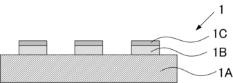
- FIG. 1A a first circuit member 1 is prepared.
- the first circuit member 1 has a base material 1A and a terminal 1B on the base material 1A. Further, the terminal 1B is subjected to a rust prevention treatment with a rust inhibitor 1C. Subsequently, as shown in FIG. 1B, the anisotropic conductive film 2 is disposed on the first circuit member 1.
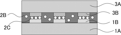
- the anisotropic conductive film 2 is formed by laminating a thermoplastic layer 2A and a conductive particle-containing layer 2B.
- the anisotropic conductive film 2 is disposed on the first circuit member 1 so that the thermoplastic layer 2 ⁇ / b> A is in contact with the terminal 1 ⁇ / b> B of the first circuit member 1.
- the conductive particle-containing layer 2B contains conductive particles 2C.
- the acid component in the thermoplastic layer 2A removes the rust inhibitor 1C from the terminal 1B.
- the second circuit member 3 is disposed on the conductive particle-containing layer 2 ⁇ / b> B of the anisotropic conductive film 2.
- the second circuit member 3 includes a base material 3A and a terminal 3B on the base material 3A.
- the second circuit member 3 is disposed on the conductive particle-containing layer 2B of the anisotropic conductive film 2 so that the terminals 3B are in contact with the conductive particle-containing layer 2B. Subsequently, as shown in FIG. 1E, the first circuit member 1 and the second circuit member 3 are connected by heating and pressing the second circuit member 3. In that case, since the rust preventive agent 1C does not exist on the terminal 1B, good connectivity is obtained. Further, since the thermoplastic layer 2A is extruded from at least between the terminal 1B and the terminal 3B during heating and pressing, the acid component in the thermoplastic layer 2A deteriorates the terminal 1B and the terminal 3B (for example, corrosion and dissolution). , Migration etc.). Therefore, the connection method of the present invention makes it possible to make a connection with excellent insulation between adjacent terminals and long-term conductivity between connection terminals even when connecting a rust-proof substrate.
- connection method of the present invention is not limited to this mode.
- the rust preventive agent is not removed from the terminal during the first arrangement step, the rust preventive agent only needs to be removed from the terminal in the heating and pressing step.
- Such an aspect is also included in the connection method of the present invention.
- a composition for the first layer was prepared. The obtained composition was applied to a release polyester film and dried by blowing hot air at 70 ° C. for 3 minutes to produce a first layer having an average thickness of 5 ⁇ m.
- Second Layer >> 45 parts by mass of phenoxy resin (manufactured by Nippon Steel Chemical Co., Ltd., trade name: YP-50), 20 parts by mass of bifunctional acrylic monomer (manufactured by Shin-Nakamura Chemical Co., Ltd., trade name: A-200), urethane acrylate (Shin Nakamura) 20 parts by mass of chemical product, product name: U-2PPA, 5 parts by mass of silica filler (average particle size 5 ⁇ m, manufactured by Nippon Aerosil Co., Ltd., product name: Aerosil RY200), dilauroyl peroxide (manufactured by NOF Corporation)
- the composition for the second layer was prepared by uniformly mixing 5 parts by mass of manufactured product name: Parroyl L) and 3 parts by mass of nickel-plated resin particles having an average particle diameter of 10 ⁇ m by a conventional method. The obtained composition was applied to a release polyester film and dried by blowing hot air at 70 ° C. for 5 minutes to produce
- the first layer and the second layer were bonded using a laminator to obtain an anisotropic conductive film having a two-layer structure.
- Example 2 An anisotropic conductive film was produced in the same manner as in Example 1 except that the average thickness of the first layer was 3 ⁇ m and the average thickness of the second layer was 32 ⁇ m.
- Example 3 An anisotropic conductive film was produced in the same manner as in Example 1 except that the composition of the first layer was changed to the composition shown in Table 1 in Example 1.
- Example 4 In Example 1, the composition of the first layer, the average thickness of the first layer, and the average thickness of the second layer were changed in the same manner as in Example 1 except that the average thickness was changed as shown in Table 1. A conductive film was produced.
- Example 5 An anisotropic conductive film was produced in the same manner as in Example 1 except that the composition of the first layer was changed as shown in Table 1 in Example 1.
- Example 6 An anisotropic conductive film was produced in the same manner as in Example 1 except that the composition of the first layer was changed as shown in Table 1 in Example 1.
- Example 1 An anisotropic conductive film was produced in the same manner as in Example 1 except that the composition of the first layer was changed as shown in Table 1 in Example 1.
- Example 2 (Comparative Example 2) In Example 1, the composition of the first layer, the average thickness of the first layer, and the average thickness of the second layer were changed in the same manner as in Example 1 except that the average thickness was changed as shown in Table 1. A conductive film was produced.
- the first circuit member PWB (Dexerials evaluation base material, 200 ⁇ m P, Cu 35 ⁇ mt—with antirust treatment, FR-4 base material)
- COF Dexerials' evaluation base material, 200 ⁇ mP, Cu 8 ⁇ mt-Sn plating, 38 ⁇ mt-S′perflex base material
- the first circuit member and the second circuit member were connected.
- the 1st circuit member used what passed the reflow furnace of Top temperature 250 degreeC 3 times.
- the anisotropic conductive film slit to a width of 2.0 mm is attached to the first circuit member so that the first layer is in contact with the terminal of the first circuit member, and the second circuit member is formed thereon.
- the heat-pressing tool buffer material 250 ⁇ mt silicon rubber, 2.0 mm width
- melt viscosity of the 1st layer and the 2nd layer in an Example and a comparative example was measured using the rheometer (made by HAAKE). The measurement was performed using each layer before bonding the first layer and the second layer using a laminator. The measurement was performed at the temperature in the flow region, and the results are shown in Table 1 as the results when the set temperature at the time of viscosity measurement was 85 ° C.
- THB evaluation was performed using the produced joined body.
- the joined body was exposed in an environment of 60 ° C.-95% RH, and a DC voltage of 50 V was applied for 250 hours. After completion of the test, it was confirmed whether or not there was a decrease in insulation due to corrosion, migration, etc., and evaluated according to the following evaluation criteria.
- the results are shown in Table 1.
- the unit of the compounding amount shown in Table 1 is part by mass.
- jER-4004P Bisphenol F type epoxy resin, manufactured by Mitsubishi Chemical Corporation YP-70: Bisphenol A / F type epoxy type phenoxy resin, manufactured by Nippon Steel Chemical Co., Ltd.
- YP-50 Bisphenol A type epoxy type phenoxy resin, Nippon Steel Chemical Co., Ltd.
- A-200 bifunctional acrylic monomer
- U-2PPA urethane acrylate, Shin-Nakamura Chemical Co., Ltd.
- PM-2 phosphate ester acrylate, Nippon Kayaku Co., Ltd.
- KE-604 rosin
- Arakawa Parroyl L Dilauroyl peroxide, manufactured by NOF Corporation Aerosil RY200: Silica filler, manufactured by Nippon Aerosil Co., Ltd.
- Example 1 the insulation between adjacent terminals and the long-term conductivity between connection terminals were excellent.
- the first layer contained an acid component, but since it contained a curing component and a curing agent, it was not a thermoplastic layer, so that the insulation resistance was insufficient. This is presumably because the first layer was not extruded from above the terminal after fabrication of the joined body, so that the acid component in the first layer damaged the terminal and caused migration at the terminal.
- the conduction resistance was insufficient. This is probably because the first layer is a thermoplastic layer but does not contain an acid component, so the rust preventive agent on the terminals could not be removed, and as a result, the rust preventive agent reduced the connectivity between the terminals. .
- the insulation resistance was insufficient. This is considered to be because the acid component damaged the terminal after the bonded body was produced, and the terminal was migrated.
- the anisotropic conductive film of the present invention is excellent in insulation between adjacent terminals and long-term conductivity between connection terminals even when connecting a substrate that has been subjected to rust prevention treatment, and thus has been subjected to rust prevention treatment. It can be suitably used for connection between a substrate and another substrate.
Landscapes
- Chemical & Material Sciences (AREA)
- Organic Chemistry (AREA)
- Engineering & Computer Science (AREA)
- Microelectronics & Electronic Packaging (AREA)
- Manufacturing & Machinery (AREA)
- Inorganic Chemistry (AREA)
- Non-Insulated Conductors (AREA)
- Adhesive Tapes (AREA)
- Adhesives Or Adhesive Processes (AREA)
- Manufacturing Of Electrical Connectors (AREA)
- Electric Connection Of Electric Components To Printed Circuits (AREA)
- Combinations Of Printed Boards (AREA)
Priority Applications (2)
| Application Number | Priority Date | Filing Date | Title |
|---|---|---|---|
| KR1020177015870A KR102006090B1 (ko) | 2015-01-22 | 2016-01-06 | 이방성 도전 필름 및 접속 방법 |
| CN201680005263.9A CN107112658B (zh) | 2015-01-22 | 2016-01-06 | 各向异性导电膜和连接方法 |
Applications Claiming Priority (2)
| Application Number | Priority Date | Filing Date | Title |
|---|---|---|---|
| JP2015-010310 | 2015-01-22 | ||
| JP2015010310A JP6474620B2 (ja) | 2015-01-22 | 2015-01-22 | 異方性導電フィルム、及び接続方法 |
Publications (1)
| Publication Number | Publication Date |
|---|---|
| WO2016117350A1 true WO2016117350A1 (ja) | 2016-07-28 |
Family
ID=56416899
Family Applications (1)
| Application Number | Title | Priority Date | Filing Date |
|---|---|---|---|
| PCT/JP2016/050191 Ceased WO2016117350A1 (ja) | 2015-01-22 | 2016-01-06 | 異方性導電フィルム、及び接続方法 |
Country Status (5)
| Country | Link |
|---|---|
| JP (1) | JP6474620B2 (https=) |
| KR (1) | KR102006090B1 (https=) |
| CN (1) | CN107112658B (https=) |
| TW (1) | TWI681694B (https=) |
| WO (1) | WO2016117350A1 (https=) |
Cited By (3)
| Publication number | Priority date | Publication date | Assignee | Title |
|---|---|---|---|---|
| WO2018225323A1 (ja) * | 2017-06-07 | 2018-12-13 | 日立化成株式会社 | 半導体用フィルム状接着剤、半導体装置の製造方法及び半導体装置 |
| JPWO2019050006A1 (ja) * | 2017-09-11 | 2020-08-20 | 日立化成株式会社 | 回路接続用接着剤フィルム及びその製造方法、回路接続構造体の製造方法、並びに、接着剤フィルム収容セット |
| KR20240158885A (ko) | 2023-04-24 | 2024-11-05 | 가부시끼가이샤 레조낙 | 반도체용 필름상 접착제, 반도체용 필름상 접착제의 제조 방법, 접착제 테이프, 반도체 장치의 제조 방법 및 반도체 장치 |
Families Citing this family (5)
| Publication number | Priority date | Publication date | Assignee | Title |
|---|---|---|---|---|
| JP6798165B2 (ja) | 2016-07-06 | 2020-12-09 | スズキ株式会社 | 車両用排気管のマウント装置 |
| KR102569980B1 (ko) * | 2017-09-11 | 2023-08-24 | 가부시끼가이샤 레조낙 | 회로 접속용 접착제 필름 및 그의 제조 방법, 회로 접속 구조체의 제조 방법, 그리고 접착제 필름 수용 세트 |
| JP6939542B2 (ja) | 2017-12-28 | 2021-09-22 | 株式会社オートネットワーク技術研究所 | 電気接続装置 |
| CN112210321A (zh) * | 2019-07-12 | 2021-01-12 | 臻鼎科技股份有限公司 | 导电粘着剂以及使用其的电磁波屏蔽膜和电路板 |
| WO2023276792A1 (ja) * | 2021-07-01 | 2023-01-05 | 日東電工株式会社 | 接合シートおよび電子部品の製造方法 |
Citations (7)
| Publication number | Priority date | Publication date | Assignee | Title |
|---|---|---|---|---|
| JPH06103819A (ja) * | 1992-09-21 | 1994-04-15 | Hitachi Chem Co Ltd | 異方導電性接着フィルム |
| JPH08148211A (ja) * | 1994-11-25 | 1996-06-07 | Hitachi Chem Co Ltd | 接続部材及び該接続部材を用いた電極の接続構造・接続方法 |
| JP2006318990A (ja) * | 2005-05-10 | 2006-11-24 | Hitachi Chem Co Ltd | 回路接続材料、回路部材の接続構造及び回路部材の接続方法。 |
| WO2008023670A1 (fr) * | 2006-08-22 | 2008-02-28 | Hitachi Chemical Company, Ltd. | matériau de connexion de circuits, structure de connexion d'un élément de circuit et procédés de fabrication de ladite structure |
| WO2009051043A1 (ja) * | 2007-10-15 | 2009-04-23 | Hitachi Chemical Company, Ltd. | 回路接続用接着フィルム及び回路接続構造体 |
| WO2013027575A1 (ja) * | 2011-08-23 | 2013-02-28 | デクセリアルズ株式会社 | 異方性導電フィルム、異方性導電フィルムの製造方法、接続方法、及び接合体 |
| WO2014156930A1 (ja) * | 2013-03-28 | 2014-10-02 | デクセリアルズ株式会社 | 回路部材の接続方法、及び接合体 |
Family Cites Families (3)
| Publication number | Priority date | Publication date | Assignee | Title |
|---|---|---|---|---|
| JP4466650B2 (ja) * | 2004-06-09 | 2010-05-26 | 日立化成工業株式会社 | フィルム状接着剤、フィルム状回路接続材、回路部材の接続方法及び半導体装置 |
| JP2009277769A (ja) | 2008-05-13 | 2009-11-26 | Hitachi Chem Co Ltd | 回路接続材料及びそれを用いた回路部材の接続構造 |
| JP5690648B2 (ja) * | 2011-04-28 | 2015-03-25 | デクセリアルズ株式会社 | 異方性導電フィルム、接続方法及び接続構造体 |
-
2015
- 2015-01-22 JP JP2015010310A patent/JP6474620B2/ja active Active
-
2016
- 2016-01-06 KR KR1020177015870A patent/KR102006090B1/ko active Active
- 2016-01-06 WO PCT/JP2016/050191 patent/WO2016117350A1/ja not_active Ceased
- 2016-01-06 CN CN201680005263.9A patent/CN107112658B/zh active Active
- 2016-01-12 TW TW105100817A patent/TWI681694B/zh active
Patent Citations (7)
| Publication number | Priority date | Publication date | Assignee | Title |
|---|---|---|---|---|
| JPH06103819A (ja) * | 1992-09-21 | 1994-04-15 | Hitachi Chem Co Ltd | 異方導電性接着フィルム |
| JPH08148211A (ja) * | 1994-11-25 | 1996-06-07 | Hitachi Chem Co Ltd | 接続部材及び該接続部材を用いた電極の接続構造・接続方法 |
| JP2006318990A (ja) * | 2005-05-10 | 2006-11-24 | Hitachi Chem Co Ltd | 回路接続材料、回路部材の接続構造及び回路部材の接続方法。 |
| WO2008023670A1 (fr) * | 2006-08-22 | 2008-02-28 | Hitachi Chemical Company, Ltd. | matériau de connexion de circuits, structure de connexion d'un élément de circuit et procédés de fabrication de ladite structure |
| WO2009051043A1 (ja) * | 2007-10-15 | 2009-04-23 | Hitachi Chemical Company, Ltd. | 回路接続用接着フィルム及び回路接続構造体 |
| WO2013027575A1 (ja) * | 2011-08-23 | 2013-02-28 | デクセリアルズ株式会社 | 異方性導電フィルム、異方性導電フィルムの製造方法、接続方法、及び接合体 |
| WO2014156930A1 (ja) * | 2013-03-28 | 2014-10-02 | デクセリアルズ株式会社 | 回路部材の接続方法、及び接合体 |
Cited By (19)
| Publication number | Priority date | Publication date | Assignee | Title |
|---|---|---|---|---|
| KR102455211B1 (ko) * | 2017-06-07 | 2022-10-14 | 쇼와덴코머티리얼즈가부시끼가이샤 | 반도체용 필름형 접착제, 반도체 장치의 제조 방법 및 반도체 장치 |
| JP2022186809A (ja) * | 2017-06-07 | 2022-12-15 | 昭和電工マテリアルズ株式会社 | 半導体用フィルム状接着剤、半導体装置の製造方法及び半導体装置 |
| WO2018225191A1 (ja) * | 2017-06-07 | 2018-12-13 | 日立化成株式会社 | 半導体用フィルム状接着剤、半導体装置の製造方法及び半導体装置 |
| JP7173002B2 (ja) | 2017-06-07 | 2022-11-16 | 昭和電工マテリアルズ株式会社 | 半導体用フィルム状接着剤、半導体装置の製造方法及び半導体装置 |
| JPWO2018225191A1 (ja) * | 2017-06-07 | 2020-04-09 | 日立化成株式会社 | 半導体用フィルム状接着剤、半導体装置の製造方法及び半導体装置 |
| JPWO2018225323A1 (ja) * | 2017-06-07 | 2020-04-09 | 日立化成株式会社 | 半導体用フィルム状接着剤、半導体装置の製造方法及び半導体装置 |
| JPWO2018225800A1 (ja) * | 2017-06-07 | 2020-04-16 | 日立化成株式会社 | 半導体用フィルム状接着剤、半導体装置の製造方法及び半導体装置 |
| TWI857859B (zh) * | 2017-06-07 | 2024-10-01 | 日商力森諾科股份有限公司 | 半導體裝置 |
| WO2018225800A1 (ja) * | 2017-06-07 | 2018-12-13 | 日立化成株式会社 | 半導体用フィルム状接着剤、半導体装置の製造方法及び半導体装置 |
| WO2018225323A1 (ja) * | 2017-06-07 | 2018-12-13 | 日立化成株式会社 | 半導体用フィルム状接着剤、半導体装置の製造方法及び半導体装置 |
| KR20200016840A (ko) * | 2017-06-07 | 2020-02-17 | 히타치가세이가부시끼가이샤 | 반도체용 필름형 접착제, 반도체 장치의 제조 방법 및 반도체 장치 |
| JP7196839B2 (ja) | 2017-06-07 | 2022-12-27 | 昭和電工マテリアルズ株式会社 | 半導体用フィルム状接着剤、基材付きフィルム状接着剤、半導体用フィルム状接着剤の製造方法、半導体装置の製造方法及び半導体装置 |
| JP2023041754A (ja) * | 2017-06-07 | 2023-03-24 | 株式会社レゾナック | 半導体用フィルム状接着剤、半導体装置の製造方法及び半導体装置 |
| TWI804062B (zh) * | 2017-06-07 | 2023-06-01 | 日商力森諾科股份有限公司 | 半導體用膜狀接著劑、半導體裝置的製造方法及半導體裝置 |
| JP7351393B2 (ja) | 2017-06-07 | 2023-09-27 | 株式会社レゾナック | 半導体用フィルム状接着剤、半導体装置の製造方法及び半導体装置 |
| JP7380926B2 (ja) | 2017-06-07 | 2023-11-15 | 株式会社レゾナック | 半導体用フィルム状接着剤、半導体装置の製造方法及び半導体装置 |
| TWI827512B (zh) * | 2017-06-07 | 2023-12-21 | 日商力森諾科股份有限公司 | 半導體用膜狀接著劑、半導體裝置的製造方法及半導體裝置 |
| JPWO2019050006A1 (ja) * | 2017-09-11 | 2020-08-20 | 日立化成株式会社 | 回路接続用接着剤フィルム及びその製造方法、回路接続構造体の製造方法、並びに、接着剤フィルム収容セット |
| KR20240158885A (ko) | 2023-04-24 | 2024-11-05 | 가부시끼가이샤 레조낙 | 반도체용 필름상 접착제, 반도체용 필름상 접착제의 제조 방법, 접착제 테이프, 반도체 장치의 제조 방법 및 반도체 장치 |
Also Published As
| Publication number | Publication date |
|---|---|
| KR20170083113A (ko) | 2017-07-17 |
| TWI681694B (zh) | 2020-01-01 |
| KR102006090B1 (ko) | 2019-07-31 |
| JP2016134366A (ja) | 2016-07-25 |
| JP6474620B2 (ja) | 2019-02-27 |
| CN107112658A (zh) | 2017-08-29 |
| CN107112658B (zh) | 2019-07-12 |
| TW201633863A (zh) | 2016-09-16 |
Similar Documents
| Publication | Publication Date | Title |
|---|---|---|
| JP6474620B2 (ja) | 異方性導電フィルム、及び接続方法 | |
| TWI655267B (zh) | Conductive adhesive and connection method of electronic parts | |
| CN1926675B (zh) | 各向异性导电连接方法及各向异性导电粘合膜 | |
| CN104822773B (zh) | 导电材料及连接结构体 | |
| JP7196839B2 (ja) | 半導体用フィルム状接着剤、基材付きフィルム状接着剤、半導体用フィルム状接着剤の製造方法、半導体装置の製造方法及び半導体装置 | |
| WO2013146604A1 (ja) | 導電材料及び接続構造体 | |
| JP7384171B2 (ja) | 半導体用フィルム状接着剤、半導体装置及びその製造方法 | |
| JP5613220B2 (ja) | 電子部品接続材料及び接続構造体 | |
| JP6328996B2 (ja) | 導電ペースト、接続構造体及び接続構造体の製造方法 | |
| WO2020241818A1 (ja) | 等方導電性粘着シート | |
| JP6133069B2 (ja) | 加熱硬化型接着フィルム | |
| HK1240406A1 (en) | Anisotropic conductive film and connection method | |
| JP6307294B2 (ja) | 回路接続材料、及び電子部品の製造方法 | |
| WO2015133211A1 (ja) | 接続構造体、接続構造体の製造方法、及び回路接続材料 | |
| TW201442584A (zh) | 回路構件之接續方法及接合體 | |
| JP6794592B1 (ja) | 等方導電性粘着シート | |
| HK1240406B (zh) | 各向异性导电膜和连接方法 | |
| JP2014067998A (ja) | 導電接続シート、端子間の接続方法、接続部の形成方法、半導体装置および電子機器 | |
| JP2015185490A (ja) | 接続構造体の製造方法、及び接続構造体 | |
| JP6286473B2 (ja) | 接合体 | |
| JP5924896B2 (ja) | 接合体の製造方法 | |
| US20190085211A1 (en) | Adhesive agent, and method for connecting electronic component |
Legal Events
| Date | Code | Title | Description |
|---|---|---|---|
| 121 | Ep: the epo has been informed by wipo that ep was designated in this application |
Ref document number: 16739957 Country of ref document: EP Kind code of ref document: A1 |
|
| ENP | Entry into the national phase |
Ref document number: 20177015870 Country of ref document: KR Kind code of ref document: A |
|
| NENP | Non-entry into the national phase |
Ref country code: DE |
|
| 122 | Ep: pct application non-entry in european phase |
Ref document number: 16739957 Country of ref document: EP Kind code of ref document: A1 |