WO2016114160A1 - 異方性導電フィルム、その製造方法及び接続構造体 - Google Patents
異方性導電フィルム、その製造方法及び接続構造体 Download PDFInfo
- Publication number
- WO2016114160A1 WO2016114160A1 PCT/JP2016/050065 JP2016050065W WO2016114160A1 WO 2016114160 A1 WO2016114160 A1 WO 2016114160A1 JP 2016050065 W JP2016050065 W JP 2016050065W WO 2016114160 A1 WO2016114160 A1 WO 2016114160A1
- Authority
- WO
- WIPO (PCT)
- Prior art keywords
- anisotropic conductive
- conductive film
- metal particles
- flux
- insulating film
- Prior art date
- Legal status (The legal status is an assumption and is not a legal conclusion. Google has not performed a legal analysis and makes no representation as to the accuracy of the status listed.)
- Ceased
Links
Images








Classifications
-
- H—ELECTRICITY
- H05—ELECTRIC TECHNIQUES NOT OTHERWISE PROVIDED FOR
- H05K—PRINTED CIRCUITS; CASINGS OR CONSTRUCTIONAL DETAILS OF ELECTRIC APPARATUS; MANUFACTURE OF ASSEMBLAGES OF ELECTRICAL COMPONENTS
- H05K3/00—Apparatus or processes for manufacturing printed circuits
- H05K3/30—Assembling printed circuits with electric components, e.g. with resistors
- H05K3/32—Assembling printed circuits with electric components, e.g. with resistors electrically connecting electric components or wires to printed circuits
- H05K3/321—Assembling printed circuits with electric components, e.g. with resistors electrically connecting electric components or wires to printed circuits by conductive adhesives
- H05K3/323—Assembling printed circuits with electric components, e.g. with resistors electrically connecting electric components or wires to printed circuits by conductive adhesives by applying an anisotropic conductive adhesive layer over an array of pads
-
- C—CHEMISTRY; METALLURGY
- C09—DYES; PAINTS; POLISHES; NATURAL RESINS; ADHESIVES; COMPOSITIONS NOT OTHERWISE PROVIDED FOR; APPLICATIONS OF MATERIALS NOT OTHERWISE PROVIDED FOR
- C09J—ADHESIVES; NON-MECHANICAL ASPECTS OF ADHESIVE PROCESSES IN GENERAL; ADHESIVE PROCESSES NOT PROVIDED FOR ELSEWHERE; USE OF MATERIALS AS ADHESIVES
- C09J5/00—Adhesive processes in general; Adhesive processes not provided for elsewhere, e.g. relating to primers
- C09J5/06—Adhesive processes in general; Adhesive processes not provided for elsewhere, e.g. relating to primers involving heating of the applied adhesive
-
- C—CHEMISTRY; METALLURGY
- C09—DYES; PAINTS; POLISHES; NATURAL RESINS; ADHESIVES; COMPOSITIONS NOT OTHERWISE PROVIDED FOR; APPLICATIONS OF MATERIALS NOT OTHERWISE PROVIDED FOR
- C09J—ADHESIVES; NON-MECHANICAL ASPECTS OF ADHESIVE PROCESSES IN GENERAL; ADHESIVE PROCESSES NOT PROVIDED FOR ELSEWHERE; USE OF MATERIALS AS ADHESIVES
- C09J7/00—Adhesives in the form of films or foils
- C09J7/30—Adhesives in the form of films or foils characterised by the adhesive composition
- C09J7/35—Heat-activated
-
- C—CHEMISTRY; METALLURGY
- C09—DYES; PAINTS; POLISHES; NATURAL RESINS; ADHESIVES; COMPOSITIONS NOT OTHERWISE PROVIDED FOR; APPLICATIONS OF MATERIALS NOT OTHERWISE PROVIDED FOR
- C09J—ADHESIVES; NON-MECHANICAL ASPECTS OF ADHESIVE PROCESSES IN GENERAL; ADHESIVE PROCESSES NOT PROVIDED FOR ELSEWHERE; USE OF MATERIALS AS ADHESIVES
- C09J9/00—Adhesives characterised by their physical nature or the effects produced, e.g. glue sticks
- C09J9/02—Electrically-conducting adhesives
-
- H—ELECTRICITY
- H01—ELECTRIC ELEMENTS
- H01B—CABLES; CONDUCTORS; INSULATORS; SELECTION OF MATERIALS FOR THEIR CONDUCTIVE, INSULATING OR DIELECTRIC PROPERTIES
- H01B1/00—Conductors or conductive bodies characterised by the conductive materials; Selection of materials as conductors
- H01B1/20—Conductive material dispersed in non-conductive organic material
- H01B1/22—Conductive material dispersed in non-conductive organic material the conductive material comprising metals or alloys
-
- H—ELECTRICITY
- H01—ELECTRIC ELEMENTS
- H01B—CABLES; CONDUCTORS; INSULATORS; SELECTION OF MATERIALS FOR THEIR CONDUCTIVE, INSULATING OR DIELECTRIC PROPERTIES
- H01B13/00—Apparatus or processes specially adapted for manufacturing conductors or cables
- H01B13/0016—Apparatus or processes specially adapted for manufacturing conductors or cables for heat treatment
-
- H—ELECTRICITY
- H01—ELECTRIC ELEMENTS
- H01B—CABLES; CONDUCTORS; INSULATORS; SELECTION OF MATERIALS FOR THEIR CONDUCTIVE, INSULATING OR DIELECTRIC PROPERTIES
- H01B13/00—Apparatus or processes specially adapted for manufacturing conductors or cables
- H01B13/0026—Apparatus for manufacturing conducting or semi-conducting layers, e.g. deposition of metal
-
- H—ELECTRICITY
- H01—ELECTRIC ELEMENTS
- H01B—CABLES; CONDUCTORS; INSULATORS; SELECTION OF MATERIALS FOR THEIR CONDUCTIVE, INSULATING OR DIELECTRIC PROPERTIES
- H01B5/00—Non-insulated conductors or conductive bodies characterised by their form
- H01B5/16—Non-insulated conductors or conductive bodies characterised by their form comprising conductive material in insulating or poorly conductive material, e.g. conductive rubber
-
- H—ELECTRICITY
- H01—ELECTRIC ELEMENTS
- H01R—ELECTRICALLY-CONDUCTIVE CONNECTIONS; STRUCTURAL ASSOCIATIONS OF A PLURALITY OF MUTUALLY-INSULATED ELECTRICAL CONNECTING ELEMENTS; COUPLING DEVICES; CURRENT COLLECTORS
- H01R11/00—Individual connecting elements providing two or more spaced connecting locations for conductive members which are, or may be, thereby interconnected, e.g. end pieces for wires or cables supported by the wire or cable and having means for facilitating electrical connection to some other wire, terminal, or conductive member, blocks of binding posts
- H01R11/01—Individual connecting elements providing two or more spaced connecting locations for conductive members which are, or may be, thereby interconnected, e.g. end pieces for wires or cables supported by the wire or cable and having means for facilitating electrical connection to some other wire, terminal, or conductive member, blocks of binding posts characterised by the form or arrangement of the conductive interconnection between the connecting locations
-
- H—ELECTRICITY
- H01—ELECTRIC ELEMENTS
- H01R—ELECTRICALLY-CONDUCTIVE CONNECTIONS; STRUCTURAL ASSOCIATIONS OF A PLURALITY OF MUTUALLY-INSULATED ELECTRICAL CONNECTING ELEMENTS; COUPLING DEVICES; CURRENT COLLECTORS
- H01R4/00—Electrically-conductive connections between two or more conductive members in direct contact, i.e. touching one another; Means for effecting or maintaining such contact; Electrically-conductive connections having two or more spaced connecting locations for conductors and using contact members penetrating insulation
- H01R4/04—Electrically-conductive connections between two or more conductive members in direct contact, i.e. touching one another; Means for effecting or maintaining such contact; Electrically-conductive connections having two or more spaced connecting locations for conductors and using contact members penetrating insulation using electrically conductive adhesives
-
- H—ELECTRICITY
- H01—ELECTRIC ELEMENTS
- H01R—ELECTRICALLY-CONDUCTIVE CONNECTIONS; STRUCTURAL ASSOCIATIONS OF A PLURALITY OF MUTUALLY-INSULATED ELECTRICAL CONNECTING ELEMENTS; COUPLING DEVICES; CURRENT COLLECTORS
- H01R43/00—Apparatus or processes specially adapted for manufacturing, assembling, maintaining, or repairing of line connectors or current collectors or for joining electric conductors
-
- H—ELECTRICITY
- H05—ELECTRIC TECHNIQUES NOT OTHERWISE PROVIDED FOR
- H05K—PRINTED CIRCUITS; CASINGS OR CONSTRUCTIONAL DETAILS OF ELECTRIC APPARATUS; MANUFACTURE OF ASSEMBLAGES OF ELECTRICAL COMPONENTS
- H05K3/00—Apparatus or processes for manufacturing printed circuits
- H05K3/30—Assembling printed circuits with electric components, e.g. with resistors
- H05K3/32—Assembling printed circuits with electric components, e.g. with resistors electrically connecting electric components or wires to printed circuits
- H05K3/34—Assembling printed circuits with electric components, e.g. with resistors electrically connecting electric components or wires to printed circuits by soldering
-
- H—ELECTRICITY
- H05—ELECTRIC TECHNIQUES NOT OTHERWISE PROVIDED FOR
- H05K—PRINTED CIRCUITS; CASINGS OR CONSTRUCTIONAL DETAILS OF ELECTRIC APPARATUS; MANUFACTURE OF ASSEMBLAGES OF ELECTRICAL COMPONENTS
- H05K3/00—Apparatus or processes for manufacturing printed circuits
- H05K3/30—Assembling printed circuits with electric components, e.g. with resistors
- H05K3/32—Assembling printed circuits with electric components, e.g. with resistors electrically connecting electric components or wires to printed circuits
- H05K3/34—Assembling printed circuits with electric components, e.g. with resistors electrically connecting electric components or wires to printed circuits by soldering
- H05K3/3465—Application of solder
- H05K3/3485—Application of solder paste, slurry or powder
-
- H—ELECTRICITY
- H10—SEMICONDUCTOR DEVICES; ELECTRIC SOLID-STATE DEVICES NOT OTHERWISE PROVIDED FOR
- H10W—GENERIC PACKAGES, INTERCONNECTIONS, CONNECTORS OR OTHER CONSTRUCTIONAL DETAILS OF DEVICES COVERED BY CLASS H10
- H10W72/00—Interconnections or connectors in packages
- H10W72/30—Die-attach connectors
-
- C—CHEMISTRY; METALLURGY
- C08—ORGANIC MACROMOLECULAR COMPOUNDS; THEIR PREPARATION OR CHEMICAL WORKING-UP; COMPOSITIONS BASED THEREON
- C08K—Use of inorganic or non-macromolecular organic substances as compounding ingredients
- C08K3/00—Use of inorganic substances as compounding ingredients
- C08K3/02—Elements
- C08K3/08—Metals
-
- C—CHEMISTRY; METALLURGY
- C09—DYES; PAINTS; POLISHES; NATURAL RESINS; ADHESIVES; COMPOSITIONS NOT OTHERWISE PROVIDED FOR; APPLICATIONS OF MATERIALS NOT OTHERWISE PROVIDED FOR
- C09J—ADHESIVES; NON-MECHANICAL ASPECTS OF ADHESIVE PROCESSES IN GENERAL; ADHESIVE PROCESSES NOT PROVIDED FOR ELSEWHERE; USE OF MATERIALS AS ADHESIVES
- C09J2301/00—Additional features of adhesives in the form of films or foils
- C09J2301/30—Additional features of adhesives in the form of films or foils characterized by the chemical, physicochemical or physical properties of the adhesive or the carrier
- C09J2301/304—Additional features of adhesives in the form of films or foils characterized by the chemical, physicochemical or physical properties of the adhesive or the carrier the adhesive being heat-activatable, i.e. not tacky at temperatures inferior to 30°C
-
- C—CHEMISTRY; METALLURGY
- C09—DYES; PAINTS; POLISHES; NATURAL RESINS; ADHESIVES; COMPOSITIONS NOT OTHERWISE PROVIDED FOR; APPLICATIONS OF MATERIALS NOT OTHERWISE PROVIDED FOR
- C09J—ADHESIVES; NON-MECHANICAL ASPECTS OF ADHESIVE PROCESSES IN GENERAL; ADHESIVE PROCESSES NOT PROVIDED FOR ELSEWHERE; USE OF MATERIALS AS ADHESIVES
- C09J2301/00—Additional features of adhesives in the form of films or foils
- C09J2301/30—Additional features of adhesives in the form of films or foils characterized by the chemical, physicochemical or physical properties of the adhesive or the carrier
- C09J2301/314—Additional features of adhesives in the form of films or foils characterized by the chemical, physicochemical or physical properties of the adhesive or the carrier the adhesive layer and/or the carrier being conductive
-
- C—CHEMISTRY; METALLURGY
- C09—DYES; PAINTS; POLISHES; NATURAL RESINS; ADHESIVES; COMPOSITIONS NOT OTHERWISE PROVIDED FOR; APPLICATIONS OF MATERIALS NOT OTHERWISE PROVIDED FOR
- C09J—ADHESIVES; NON-MECHANICAL ASPECTS OF ADHESIVE PROCESSES IN GENERAL; ADHESIVE PROCESSES NOT PROVIDED FOR ELSEWHERE; USE OF MATERIALS AS ADHESIVES
- C09J2301/00—Additional features of adhesives in the form of films or foils
- C09J2301/40—Additional features of adhesives in the form of films or foils characterized by the presence of essential components
- C09J2301/408—Additional features of adhesives in the form of films or foils characterized by the presence of essential components additives as essential feature of the adhesive layer
-
- H—ELECTRICITY
- H05—ELECTRIC TECHNIQUES NOT OTHERWISE PROVIDED FOR
- H05K—PRINTED CIRCUITS; CASINGS OR CONSTRUCTIONAL DETAILS OF ELECTRIC APPARATUS; MANUFACTURE OF ASSEMBLAGES OF ELECTRICAL COMPONENTS
- H05K2203/00—Indexing scheme relating to apparatus or processes for manufacturing printed circuits covered by H05K3/00
- H05K2203/04—Soldering or other types of metallurgic bonding
- H05K2203/0425—Solder powder or solder coated metal powder
-
- H—ELECTRICITY
- H10—SEMICONDUCTOR DEVICES; ELECTRIC SOLID-STATE DEVICES NOT OTHERWISE PROVIDED FOR
- H10W—GENERIC PACKAGES, INTERCONNECTIONS, CONNECTORS OR OTHER CONSTRUCTIONAL DETAILS OF DEVICES COVERED BY CLASS H10
- H10W72/00—Interconnections or connectors in packages
- H10W72/01—Manufacture or treatment
- H10W72/013—Manufacture or treatment of die-attach connectors
-
- H—ELECTRICITY
- H10—SEMICONDUCTOR DEVICES; ELECTRIC SOLID-STATE DEVICES NOT OTHERWISE PROVIDED FOR
- H10W—GENERIC PACKAGES, INTERCONNECTIONS, CONNECTORS OR OTHER CONSTRUCTIONAL DETAILS OF DEVICES COVERED BY CLASS H10
- H10W72/00—Interconnections or connectors in packages
- H10W72/01—Manufacture or treatment
- H10W72/0198—Manufacture or treatment batch processes
-
- H—ELECTRICITY
- H10—SEMICONDUCTOR DEVICES; ELECTRIC SOLID-STATE DEVICES NOT OTHERWISE PROVIDED FOR
- H10W—GENERIC PACKAGES, INTERCONNECTIONS, CONNECTORS OR OTHER CONSTRUCTIONAL DETAILS OF DEVICES COVERED BY CLASS H10
- H10W72/00—Interconnections or connectors in packages
- H10W72/071—Connecting or disconnecting
- H10W72/072—Connecting or disconnecting of bump connectors
-
- H—ELECTRICITY
- H10—SEMICONDUCTOR DEVICES; ELECTRIC SOLID-STATE DEVICES NOT OTHERWISE PROVIDED FOR
- H10W—GENERIC PACKAGES, INTERCONNECTIONS, CONNECTORS OR OTHER CONSTRUCTIONAL DETAILS OF DEVICES COVERED BY CLASS H10
- H10W72/00—Interconnections or connectors in packages
- H10W72/071—Connecting or disconnecting
- H10W72/073—Connecting or disconnecting of die-attach connectors
-
- H—ELECTRICITY
- H10—SEMICONDUCTOR DEVICES; ELECTRIC SOLID-STATE DEVICES NOT OTHERWISE PROVIDED FOR
- H10W—GENERIC PACKAGES, INTERCONNECTIONS, CONNECTORS OR OTHER CONSTRUCTIONAL DETAILS OF DEVICES COVERED BY CLASS H10
- H10W72/00—Interconnections or connectors in packages
- H10W72/071—Connecting or disconnecting
- H10W72/073—Connecting or disconnecting of die-attach connectors
- H10W72/07331—Connecting techniques
- H10W72/07332—Compression bonding, e.g. thermocompression bonding
-
- H—ELECTRICITY
- H10—SEMICONDUCTOR DEVICES; ELECTRIC SOLID-STATE DEVICES NOT OTHERWISE PROVIDED FOR
- H10W—GENERIC PACKAGES, INTERCONNECTIONS, CONNECTORS OR OTHER CONSTRUCTIONAL DETAILS OF DEVICES COVERED BY CLASS H10
- H10W72/00—Interconnections or connectors in packages
- H10W72/071—Connecting or disconnecting
- H10W72/073—Connecting or disconnecting of die-attach connectors
- H10W72/07331—Connecting techniques
- H10W72/07337—Connecting techniques using a polymer adhesive, e.g. an adhesive based on silicone or epoxy
- H10W72/07338—Connecting techniques using a polymer adhesive, e.g. an adhesive based on silicone or epoxy hardening the adhesive by curing, e.g. thermosetting
-
- H—ELECTRICITY
- H10—SEMICONDUCTOR DEVICES; ELECTRIC SOLID-STATE DEVICES NOT OTHERWISE PROVIDED FOR
- H10W—GENERIC PACKAGES, INTERCONNECTIONS, CONNECTORS OR OTHER CONSTRUCTIONAL DETAILS OF DEVICES COVERED BY CLASS H10
- H10W72/00—Interconnections or connectors in packages
- H10W72/071—Connecting or disconnecting
- H10W72/073—Connecting or disconnecting of die-attach connectors
- H10W72/07331—Connecting techniques
- H10W72/07337—Connecting techniques using a polymer adhesive, e.g. an adhesive based on silicone or epoxy
- H10W72/07339—Connecting techniques using a polymer adhesive, e.g. an adhesive based on silicone or epoxy hardening the adhesive by cooling, e.g. thermoplastics
-
- H—ELECTRICITY
- H10—SEMICONDUCTOR DEVICES; ELECTRIC SOLID-STATE DEVICES NOT OTHERWISE PROVIDED FOR
- H10W—GENERIC PACKAGES, INTERCONNECTIONS, CONNECTORS OR OTHER CONSTRUCTIONAL DETAILS OF DEVICES COVERED BY CLASS H10
- H10W72/00—Interconnections or connectors in packages
- H10W72/071—Connecting or disconnecting
- H10W72/074—Connecting or disconnecting of anisotropic conductive adhesives
-
- H—ELECTRICITY
- H10—SEMICONDUCTOR DEVICES; ELECTRIC SOLID-STATE DEVICES NOT OTHERWISE PROVIDED FOR
- H10W—GENERIC PACKAGES, INTERCONNECTIONS, CONNECTORS OR OTHER CONSTRUCTIONAL DETAILS OF DEVICES COVERED BY CLASS H10
- H10W72/00—Interconnections or connectors in packages
- H10W72/20—Bump connectors, e.g. solder bumps or copper pillars; Dummy bumps; Thermal bumps
- H10W72/241—Dispositions, e.g. layouts
-
- H—ELECTRICITY
- H10—SEMICONDUCTOR DEVICES; ELECTRIC SOLID-STATE DEVICES NOT OTHERWISE PROVIDED FOR
- H10W—GENERIC PACKAGES, INTERCONNECTIONS, CONNECTORS OR OTHER CONSTRUCTIONAL DETAILS OF DEVICES COVERED BY CLASS H10
- H10W72/00—Interconnections or connectors in packages
- H10W72/20—Bump connectors, e.g. solder bumps or copper pillars; Dummy bumps; Thermal bumps
- H10W72/251—Materials
- H10W72/252—Materials comprising solid metals or solid metalloids, e.g. PbSn, Ag or Cu
-
- H—ELECTRICITY
- H10—SEMICONDUCTOR DEVICES; ELECTRIC SOLID-STATE DEVICES NOT OTHERWISE PROVIDED FOR
- H10W—GENERIC PACKAGES, INTERCONNECTIONS, CONNECTORS OR OTHER CONSTRUCTIONAL DETAILS OF DEVICES COVERED BY CLASS H10
- H10W72/00—Interconnections or connectors in packages
- H10W72/20—Bump connectors, e.g. solder bumps or copper pillars; Dummy bumps; Thermal bumps
- H10W72/261—Functions other than electrical connecting
-
- H—ELECTRICITY
- H10—SEMICONDUCTOR DEVICES; ELECTRIC SOLID-STATE DEVICES NOT OTHERWISE PROVIDED FOR
- H10W—GENERIC PACKAGES, INTERCONNECTIONS, CONNECTORS OR OTHER CONSTRUCTIONAL DETAILS OF DEVICES COVERED BY CLASS H10
- H10W72/00—Interconnections or connectors in packages
- H10W72/30—Die-attach connectors
- H10W72/321—Structures or relative sizes of die-attach connectors
- H10W72/322—Multilayered die-attach connectors, e.g. a coating on a top surface of a core
-
- H—ELECTRICITY
- H10—SEMICONDUCTOR DEVICES; ELECTRIC SOLID-STATE DEVICES NOT OTHERWISE PROVIDED FOR
- H10W—GENERIC PACKAGES, INTERCONNECTIONS, CONNECTORS OR OTHER CONSTRUCTIONAL DETAILS OF DEVICES COVERED BY CLASS H10
- H10W72/00—Interconnections or connectors in packages
- H10W72/30—Die-attach connectors
- H10W72/321—Structures or relative sizes of die-attach connectors
- H10W72/325—Die-attach connectors having a filler embedded in a matrix
-
- H—ELECTRICITY
- H10—SEMICONDUCTOR DEVICES; ELECTRIC SOLID-STATE DEVICES NOT OTHERWISE PROVIDED FOR
- H10W—GENERIC PACKAGES, INTERCONNECTIONS, CONNECTORS OR OTHER CONSTRUCTIONAL DETAILS OF DEVICES COVERED BY CLASS H10
- H10W72/00—Interconnections or connectors in packages
- H10W72/30—Die-attach connectors
- H10W72/351—Materials of die-attach connectors
-
- H—ELECTRICITY
- H10—SEMICONDUCTOR DEVICES; ELECTRIC SOLID-STATE DEVICES NOT OTHERWISE PROVIDED FOR
- H10W—GENERIC PACKAGES, INTERCONNECTIONS, CONNECTORS OR OTHER CONSTRUCTIONAL DETAILS OF DEVICES COVERED BY CLASS H10
- H10W72/00—Interconnections or connectors in packages
- H10W72/30—Die-attach connectors
- H10W72/351—Materials of die-attach connectors
- H10W72/352—Materials of die-attach connectors comprising metals or metalloids, e.g. solders
-
- H—ELECTRICITY
- H10—SEMICONDUCTOR DEVICES; ELECTRIC SOLID-STATE DEVICES NOT OTHERWISE PROVIDED FOR
- H10W—GENERIC PACKAGES, INTERCONNECTIONS, CONNECTORS OR OTHER CONSTRUCTIONAL DETAILS OF DEVICES COVERED BY CLASS H10
- H10W72/00—Interconnections or connectors in packages
- H10W72/30—Die-attach connectors
- H10W72/351—Materials of die-attach connectors
- H10W72/353—Materials of die-attach connectors not comprising solid metals or solid metalloids, e.g. ceramics
-
- H—ELECTRICITY
- H10—SEMICONDUCTOR DEVICES; ELECTRIC SOLID-STATE DEVICES NOT OTHERWISE PROVIDED FOR
- H10W—GENERIC PACKAGES, INTERCONNECTIONS, CONNECTORS OR OTHER CONSTRUCTIONAL DETAILS OF DEVICES COVERED BY CLASS H10
- H10W72/00—Interconnections or connectors in packages
- H10W72/30—Die-attach connectors
- H10W72/351—Materials of die-attach connectors
- H10W72/353—Materials of die-attach connectors not comprising solid metals or solid metalloids, e.g. ceramics
- H10W72/354—Materials of die-attach connectors not comprising solid metals or solid metalloids, e.g. ceramics comprising polymers
-
- H—ELECTRICITY
- H10—SEMICONDUCTOR DEVICES; ELECTRIC SOLID-STATE DEVICES NOT OTHERWISE PROVIDED FOR
- H10W—GENERIC PACKAGES, INTERCONNECTIONS, CONNECTORS OR OTHER CONSTRUCTIONAL DETAILS OF DEVICES COVERED BY CLASS H10
- H10W90/00—Package configurations
- H10W90/701—Package configurations characterised by the relative positions of pads or connectors relative to package parts
- H10W90/731—Package configurations characterised by the relative positions of pads or connectors relative to package parts of die-attach connectors
- H10W90/732—Package configurations characterised by the relative positions of pads or connectors relative to package parts of die-attach connectors between stacked chips
-
- H—ELECTRICITY
- H10—SEMICONDUCTOR DEVICES; ELECTRIC SOLID-STATE DEVICES NOT OTHERWISE PROVIDED FOR
- H10W—GENERIC PACKAGES, INTERCONNECTIONS, CONNECTORS OR OTHER CONSTRUCTIONAL DETAILS OF DEVICES COVERED BY CLASS H10
- H10W90/00—Package configurations
- H10W90/701—Package configurations characterised by the relative positions of pads or connectors relative to package parts
- H10W90/731—Package configurations characterised by the relative positions of pads or connectors relative to package parts of die-attach connectors
- H10W90/734—Package configurations characterised by the relative positions of pads or connectors relative to package parts of die-attach connectors between a chip and a stacked insulating package substrate, interposer or RDL
-
- H—ELECTRICITY
- H10—SEMICONDUCTOR DEVICES; ELECTRIC SOLID-STATE DEVICES NOT OTHERWISE PROVIDED FOR
- H10W—GENERIC PACKAGES, INTERCONNECTIONS, CONNECTORS OR OTHER CONSTRUCTIONAL DETAILS OF DEVICES COVERED BY CLASS H10
- H10W99/00—Subject matter not provided for in other groups of this subclass
Definitions
- the present invention relates to an anisotropic conductive film in which metal particles and a flux are present in contact with or close to each other in the film.
- Patent Document 1 It has been proposed to use an anisotropic conductive film in which conductive particles having a nickel / gold plating layer formed on the surface of a resin core are dispersed in an insulating adhesive composition when an IC chip is mounted on a substrate.
- Patent Document 1 the conductive particles are crushed between the terminals of the IC chip and the terminals of the substrate, or the conductive particles bite into the respective terminals to ensure conduction, and the insulating adhesive composition is used for the IC chip, the substrate, and the conductive particles. And are fixed.
- connection structure obtained by connecting the IC chip to the substrate using an anisotropic conductive film is high temperature and high pressure. Or, when stored in a high-temperature and high-humidity environment, there is a problem that conduction reliability is lowered.
- the conductive particles of the anisotropic conductive film it is possible to employ solder particles that form a metal bond with copper or the like at a relatively low temperature as compared with metals such as copper and aluminum that are widely used as terminal materials for IC chips. It is considered.
- An object of the present invention is to solve the above-described problems of the prior art, and an anisotropic conductive film having metal particles such as solder particles having an oxide film on the surface as conductive particles for anisotropic conductive connection. In this case, it is possible to suppress occurrence of a short circuit and to realize high conduction reliability.
- the present inventors have used metal particles in order to suppress the occurrence of short circuit. Rather than randomly dispersing in the insulating adhesive composition, the anisotropic conductive film should be regularly arranged when viewed in plan, and in order to achieve high conduction reliability, the flux in the film Has been found to be present in contact with or close to the metal particles, and the present invention has been completed.
- the present invention is an anisotropic conductive film having metal particles in an insulating film, wherein the metal particles are regularly arranged in a plan view, and the anisotropic conductive film surface side end of the metal particles or a different surface.
- an anisotropic conductive film in which a flux is disposed so as to be in contact with or close to at least one of the end portions on the back side of the isotropic conductive film.
- the present invention also relates to a method for producing the above anisotropic conductive film, which comprises the following steps (A) to (C): (A) a step of disposing a flux on at least the bottom of the concave portion of the transfer mold having the concave portions arranged regularly; (B) a step of placing metal particles in the recesses in which the flux is disposed; and (C) the insulating film is brought into contact with the insulating film from the recess side of the transfer mold in which the metal particles are disposed, and the metal particles are applied to the insulating film by heating and pressing.
- a production method is provided. This production method preferably further comprises step (D) (D) There is a step of thermocompression bonding another insulating film to the metal particle transfer surface of the insulating film to which the metal particles have been transferred.
- the present invention is another method for producing the above-mentioned anisotropic conductive film, which comprises the following steps (a) to (d): (A) a step of disposing metal particles in the recesses of the transfer mold having regularly arranged recesses; (B) a step of disposing a flux on a recess forming surface on which transfer-type metal particles are disposed; (C) a step of bringing the insulating film into contact with the transfer-type flux arrangement surface side and applying heat and pressure to transfer the metal particles to the insulating film; , Thermocompression bonding another insulating film; Have
- the present invention provides the first electronic component by disposing the aforementioned anisotropic conductive film disposed between the terminal of the first electronic component and the terminal of the second electronic component, and heating and pressing the first electronic component.
- a connection structure in which the second electronic component and the second electronic component are anisotropically conductively connected.
- the metal particles are regularly arranged in a plan view, so that the occurrence of short-circuits can be suppressed when applied to anisotropic conductive connection. it can. Also, since the flux is arranged so that the flux contacts or is close to at least one of the anisotropic conductive film surface side end portion or the anisotropic conductive film back surface side end portion of the metal particles, The oxide film on the surface of the metal particles can be removed at the time of conductive connection, and high conduction reliability can be realized.
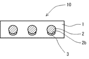
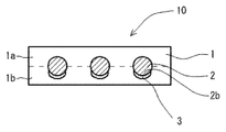
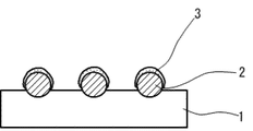
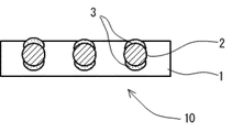
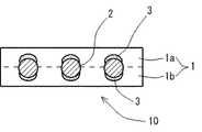
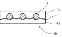
- FIG. 1A is a cross-sectional view of the anisotropic conductive film of the present invention.
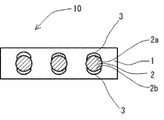
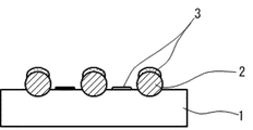
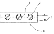
- FIG. 1B is a cross-sectional view of the anisotropic conductive film of the present invention.
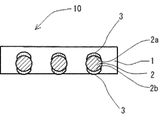
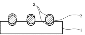
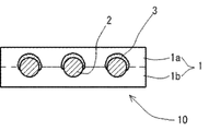
- FIG. 1C is a cross-sectional view of the anisotropic conductive film of the present invention.
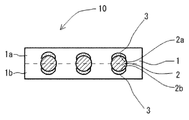
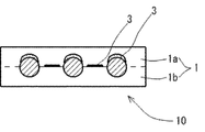
- FIG. 2A is a cross-sectional view of the anisotropic conductive film of the present invention.
- FIG. 2B is a cross-sectional view of the anisotropic conductive film of the present invention.
- FIG. 2C is a cross-sectional view of the anisotropic conductive film of the present invention.
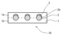
- FIG. 3 is a cross-sectional view of the anisotropic conductive film of the present invention.
- FIG. 4 is a cross-sectional view of the anisotropic conductive film of the present invention.
- FIG. 5 is a cross-sectional view of the anisotropic conductive film of the present invention.
- FIG. 6 is a cross-sectional view of the anisotropic conductive film of the present invention.
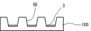
- FIG. 7A is a process explanatory diagram of the method for producing an anisotropic conductive film of the present invention.
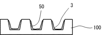
- FIG. 7B is a process explanatory diagram of the method for producing an anisotropic conductive film of the present invention.
- FIG. 7C is a process explanatory diagram of the method for producing an anisotropic conductive film of the present invention.
- FIG. 7A is a process explanatory diagram of the method for producing an anisotropic conductive film of the present invention.
- FIG. 7B is a process explanatory diagram of the method for producing an anisotropic conductive film of the present invention.
- FIG. 7C is a process explanatory diagram of
- FIG. 8A is a process explanatory diagram of the method for producing an anisotropic conductive film of the present invention.
- FIG. 8B is a process explanatory diagram of the method for producing an anisotropic conductive film of the present invention.
- FIG. 8C is a process explanatory diagram of the method for producing an anisotropic conductive film of the present invention.
- FIG. 8D is a process explanatory diagram of the method for producing an anisotropic conductive film of the present invention.
- FIG. 9A is a process explanatory diagram of the method for producing an anisotropic conductive film of the present invention.
- FIG. 9B is a process explanatory diagram of the method for producing an anisotropic conductive film of the present invention.
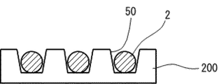
- FIG. 9C is a process explanatory diagram of the method for producing an anisotropic conductive film of the present invention.
- FIG. 9D is a process explanatory diagram of the method for producing an anisotropic conductive film of the present invention.
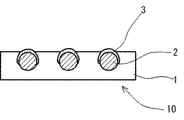
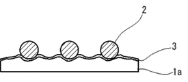
- FIG. 10A is a cross-sectional view of the anisotropic conductive film of the present invention.
- FIG. 10B is a cross-sectional view of the anisotropic conductive film of the present invention.
- FIG. 10C is a cross-sectional view of the anisotropic conductive film of the present invention.
- FIG. 10D is a cross-sectional view of the anisotropic conductive film of the present invention.
- FIG. 11A is a cross-sectional view of the anisotropic conductive film of the present invention.
- FIG. 11B is a cross-sectional view of the anisotropic conductive film of the present invention.
- FIG. 11C is a cross-sectional view of the anisotropic conductive film of the present invention.
- FIG. 11D is a cross-sectional view of the anisotropic conductive film of the present invention.
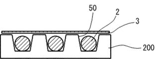
- FIG. 12A is a process explanatory diagram of the method for producing an anisotropic conductive film of the present invention.
- FIG. 12B is a process explanatory diagram of the method for producing an anisotropic conductive film of the present invention.
- FIG. 12C is a process explanatory diagram of the method for producing an anisotropic conductive film of the present invention.
- FIG. 12D is a process explanatory diagram of the method for producing an anisotropic conductive film of the present invention.
- the insulating film 1 can be used by appropriately selecting from the insulating films employed in conventionally known anisotropic conductive films.
- a thermoplastic acrylic or epoxy resin film, a thermosetting or photocuring acrylic or epoxy resin film, and the like can be given.
- the thickness of such an insulating film is usually 10 to 40 ⁇ m.
- the insulating film 1 should just be a film in the state of an anisotropic conductive film at least, and may be a highly viscous liquid at the time of the manufacture.
- the metal particles 2 are used as anisotropic conductive film metal particles in an anisotropic conductive film and can be used by appropriately selecting from those having an oxide film formed on the surface. it can. Among these, solder particles having an average particle diameter of 10 to 40 ⁇ m when measured with an image type particle size distribution meter are preferred.
- the flux 3 is in contact with or close to at least one end of the anisotropic conductive film surface side end or the anisotropic conductive film back side end of the metal particles. Is arranged.
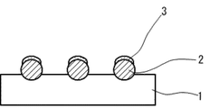
- the flux 3 is arranged so as to contact the anisotropic conductive film surface side end 2 a of the metal particles 2.
- the flux 3 is disposed so as to contact the anisotropic conductive film back surface side end 2 b of the metal particles 2.
- FIG. 1A the flux 3 is disposed so as to contact the anisotropic conductive film back surface side end 2 b of the metal particles 2.
- the flux 3 is arranged so as to contact the anisotropic conductive film surface side end 2 a and the anisotropic conductive film back side end 2 b of the metal particles 2. As described above, when the metal particles 2 and the flux 3 are in contact with each other, the oxide film on the surface of the metal particles 2 is removed by the flux 3 by the heat in the anisotropic conductive connection, and the metal particles 2 are connected. A metal bond is formed with the terminal to be.
- the quantitative relationship between the metal particles 2 and the flux 3 in contact with or close to the metal particles 2 is such that the thickness of the flux 3 is 0.001 to 0.4 times the average particle diameter of the metal particles 2. If it is this range, the surface of the metal particle 2 can be cleaned and an anisotropic conductive connection thing will not be corroded.
- the flux 3 When the flux 3 is placed in contact with or close to the metal particles 2, the flux diluted in a solvent (preferred dilution ratio: 0.1 to 40 wt% with respect to the solvent) What is necessary is just to apply
- the flux 3 removes the oxide film on the surface of the metal particles 2 under the heating condition in the anisotropic conductive connection.
- a known flux according to the material of the metal particles 2 can be applied.
- the insulating film 1 is a single layer. However, as shown in FIG. 3, the insulating film 1 has a two-layer structure (1a and 1b), and a metal is interposed between these layers. Particles 2 may be arranged. With such a two-layer structure, the manufacturing flexibility can be expanded.
- the anisotropic conductive film 10 of the present invention includes an embodiment in which a part of the surface of the metal particle 2 is not in contact with the flux 3.
- the surface portion of the metal particle 2 that is not in contact with the flux 3 faces the side surface direction of the film, but may face the front surface side of the film or may face the back surface side.
- the surface portion of the metal particles 2 that is not in contact with the flux 3 is preferably disposed on the opposite side of the surface portion of the metal particles that are in contact with the flux.
- the flux 3 may be arrange
- the flux 3 disposed between the adjacent metal particles 2 is attracted to the metal particles 2 at the time of anisotropic conductive connection.
- the surface of the particles can be cleaned and delamination of the insulating film having a two-layer structure does not occur.
- the amount of flux per unit area arranged at least one of the anisotropic conductive film surface side end 2a or the anisotropic conductive film back side end 2b of the metal particles 2 is adjacent.
- the amount of flux per unit area disposed between the metal particles 2 is preferably larger.
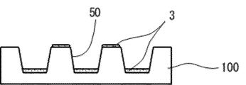
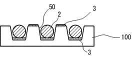
- the flux 3 is disposed on at least the bottom of the recess 50 of the transfer mold 100 having the recesses 50 arranged regularly. Specifically, as shown in FIG. 7A, the flux 3 may be disposed only at the bottom of the recess 50, or as shown in FIG. 7B, the flux 3 may be disposed on the entire inner wall surface including the bottom of the recess 50. Good. Further, as shown in FIG. 7C, the flux 3 may be disposed on the bottom of the recess 50 and the surface between the adjacent recesses 50 of the transfer body 100. In the case of FIG. 7C, the amount of flux per unit area at the bottom of the recess 50 is preferably larger than the amount of flux per unit area of the surface between adjacent recesses 50.
- the flux 3 is applied to the entire surface of the transfer mold by a screen printing method, and the flux on the outermost surface is applied if necessary. Scraping with a blade.
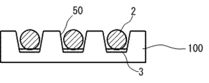
- the metal particles 2 are arranged in the recesses 50 in which the flux 3 is arranged.
- a known method can be employed.
- metal particles may be dispersed on the surface of the transfer mold, and the metal particles present on the transfer mold surface other than the recesses may be removed by air blow or a blade.
- you may supply a metal particle to a recessed part one by one with a micro dispenser.
- the flux 3 may be arranged on the surface of the metal particles 2 by using a process technique as shown in FIG. 8D.
- FIGS. 9A to 9D the insulating film 1 is brought into contact with the transfer mold 100 (FIGS. 8A to 8D) of FIGS.
- the metal particles 2 are transferred to the insulating film 1 by applying pressure. If the insulating film 1 is wound around the roll in this state, the anisotropic conductive film 10 of FIG. 10A is obtained from the embodiment of FIG. 9A, and the anisotropic conductive film 10 of FIG. 10B is obtained from the embodiment of FIG. 9C is obtained, and the anisotropic conductive film 10 of FIG. 10C is obtained from the embodiment of FIG. 9C, and the anisotropic conductive film 10 of FIG. 10D is obtained from the embodiment of FIG. 9D.
- step (D) in order to make the insulating film have a two-layer structure.
- the anisotropic conductive film of the present invention can also be produced by another production method having the following steps (a) to (c).
- the metal particles 2 are arranged in the recesses 50 of the transfer mold 200 having the recesses 50 arranged in a regular arrangement.
- the anisotropic conductive film of the present invention is disposed between a terminal of a first electronic component such as an IC chip or a semiconductor wafer and a terminal of a second electronic component such as a wiring board or a halfway wafer, and is heated. It is useful for manufacturing a connection structure in which the first electronic component and the second electronic component are anisotropically conductively connected by applying pressure. Such a connection structure is also one embodiment of the present invention.
- Example 1 A nickel plate having a thickness of 2 mm was prepared, and cylindrical convex portions (outer diameter 25 ⁇ m, height 20 ⁇ m) were formed in a tetragonal lattice pattern to obtain a transfer material master. The distance between the centers of adjacent convex portions was 40 ⁇ m. Therefore, the density of the convex portions was 625 pieces / mm 2 .
- a flux (ESR-250T4, Senju Metal Industry Co., Ltd.) diluted with toluene using a squeegee is applied to the transfer mold peeled off from the transfer mold master, and the flux thickness in the recess becomes 1 ⁇ m after drying. The flux on the surface of the transfer mold was scraped off.
- solder particles fine solder powder, Mitsui Mining & Smelting Co., Ltd.
- the recesses were filled with solder particles by air blowing.
- insulating film 60 ⁇ m of insulating film (phenoxy resin (YP-50, Nippon Steel & Sumikin Chemical Co., Ltd.) with a thickness of 20 ⁇ m, epoxy resin (jER828, Mitsubishi Chemical Co., Ltd.) on the transfer type solder particle adhesion surface to which conductive particles have adhered. ) 40 parts by weight, and a cationic curing agent (SI-60L, Sanshin Chemical Industry Co., Ltd.) 2 parts by weight), and press at a temperature of 50 ° C. and a pressure of 0.5 MPa to form an insulating film. Solder particles were transferred.
- Example 2 A transfer mold similar to that of Example 1 was prepared. Solder particles (fine solder powder, Mitsui Mining & Smelting Co., Ltd.) having an average particle diameter of 20 ⁇ m were sprayed on the transfer mold, and then air blowed to form solder particles in the recesses. Filled.
- Solder particles fine solder powder, Mitsui Mining & Smelting Co., Ltd.
- a flux diluted to 20 wt% with toluene using a squeegee was applied to the surface of the transfer mold filled with solder particles so that the flux thickness after drying was 1 ⁇ m. .
- An insulating film (phenoxy resin (YP-50, Nippon Steel & Sumikin Chemical Co., Ltd.) 60 parts by mass, epoxy resin (jER828, Mitsubishi Chemical Co., Ltd.) 40 parts by mass, and cationic curing with respect to the flux surface
- An agent (SI-60L, a film consisting of 2 parts by mass of Sanshin Chemical Industry Co., Ltd.) was placed and pressed at a temperature of 50 ° C. and a pressure of 0.5 MPa to transfer the solder particles to the insulating film.
- Comparative Example 1 An anisotropic conductive film was obtained by repeating Example 1 except that no flux was used.
- Example 3 A transfer mold similar to that in Example 1 was prepared, and a flux was disposed on the bottom of the recess of the transfer mold in the same manner as in Example 1. Then, the recess was filled with solder particles. On the surface of the transfer mold, a flux (ESR-250T4, Senju Metal Industry Co., Ltd.) diluted to 5 wt% with toluene was applied again using a squeegee. Then, the anisotropic conductive film was obtained by repeating the same operation as Example 1. The coating thickness after drying of the flux was 1 ⁇ m at the end of the solder particles on the film interface side, and less than 1 ⁇ m between the solder particles.
- ESR-250T4 Senju Metal Industry Co., Ltd.
- Example 4 Example 1 is repeated except that the dilution of the flux (ESR-250T4, Senju Metal Industry Co., Ltd.) with toluene is changed from 5 wt% to 10 wt% in Example 1 and the coating thickness after drying is changed to 2 ⁇ m. Thus, an anisotropic conductive film was obtained.
- ESR-250T4, Senju Metal Industry Co., Ltd. Senju Metal Industry Co., Ltd.
- the initial conduction resistance value needs to be less than 1 ⁇
- the conduction resistance value after PCT and after the high temperature and high humidity bias test needs to be less than 15 ⁇ .
Landscapes
- Engineering & Computer Science (AREA)
- Chemical & Material Sciences (AREA)
- Manufacturing & Machinery (AREA)
- Organic Chemistry (AREA)
- Microelectronics & Electronic Packaging (AREA)
- Physics & Mathematics (AREA)
- Spectroscopy & Molecular Physics (AREA)
- Dispersion Chemistry (AREA)
- Thermal Sciences (AREA)
- Non-Insulated Conductors (AREA)
- Adhesives Or Adhesive Processes (AREA)
- Manufacturing Of Electrical Connectors (AREA)
- Conductive Materials (AREA)
Abstract
Description
(A)規則配列された凹部を有する転写型の当該凹部の少なくとも底部にフラックスを配置する工程;
(B)フラックスが配置された凹部に金属粒子を配置する工程;及び
(C)金属粒子が配置された転写型の凹部側より絶縁フィルムを当接させて加熱加圧して絶縁フィルムに金属粒子を転写する工程;
を有する製造方法を提供する。この製造方法は、好ましくは、更に工程(D)
(D)金属粒子が転写された絶縁フィルムの金属粒子転写面に、別の絶縁フィルムを熱圧着する工程
を有する。
(a)規則配列された凹部を有する転写型の当該凹部に金属粒子を配置する工程;
(b)転写型の金属粒子が配置された凹部形成面にフラックスを配置する工程;
(c)転写型のフラックス配置面側より絶縁フィルムを当接させて加熱加圧して絶縁フィルムに金属粒子を転写する工程;及び
(d)金属粒子が転写された絶縁フィルムの金属粒子転写面に、別の絶縁フィルムを熱圧着する工程;
を有する。
以下、本発明の具体例を図面を参照しながら説明する。
本発明の異方性導電フィルムは、以下の工程(A)~(C)を有する製造方法により製造することができる。
まず、図7A~図7Cに示すように、規則配列された凹部50を有する転写型100の当該凹部50の少なくとも底部にフラックス3を配置する。具体的には、図7Aに示すように、凹部50の底部だけにフラックス3を配置してよく、図7Bに示すように、凹部50の底部を含む内壁面全体にフラックス3を配置してもよい。また、図7Cに示すように、凹部50の底部と、転写体100の隣接凹部50間の表面とにフラックス3を配置してもよい。図7Cの場合、凹部50の底部の単位面積当たりのフラックス量が、隣接凹部50間の表面の単位面積当たりのフラックス量より大とすることが好ましい。
次に、図8A~図8Cに示すように、フラックス3が配置された凹部50に金属粒子2を配置する。金属粒子2を配置する手法としては、公知の手法を採用することができる。例えば、転写型の表面に金属粒子を散布し、凹部以外の転写型表面に存在する金属粒子をエアブローやブレードで除去すればよい。また、マイクロディスペンサーにより凹部に金属粒子を一個ずつ供給してもよい。
次に、図9A~図9Dに示すように、金属粒子2が配置された図8A~図8Dの転写型100(図8A~図8D)の凹部50側より絶縁フィルム1を当接させて加熱加圧して絶縁フィルム1に金属粒子2を転写する。この状態で、絶縁フィルム1をロールに巻き締めれば、図9Aの態様からは、図10Aの異方性導電フィルム10が得られ、図9Bの態様からは、図10Bの異方性導電フィルム10が得られ、図9Cの態様からは、図10Cの異方性導電フィルム10が得られ、そして図9Dの態様からは、図10Dの異方性導電フィルム10が得られる。
即ち、金属粒子が転写された絶縁フィルム(図9A~図9D)の金属粒子転写面に、別の絶縁フィルムを熱圧着することにより、図9Aの態様からは、2層構造の絶縁フィルム1(1aと1b)を有する図11Aの異方性導電フィルム10が得られ、図9Bの態様からは、2層構造の絶縁フィルム1(1aと1b)を有する図11Bの異方性導電フィルム10が得られ、図9Cの態様からは、2層構造の絶縁フィルム1(1aと1b)を有する図11Cの異方性導電フィルム10が得られ、そして図9Dの態様からは、2層構造の絶縁フィルム1(1aと1b)を有する図11Dの異方性導電フィルム10が得られる。
まず、図12Aに示すように、規則配列された凹部50を有する転写型200の当該凹部50に金属粒子2を配置する。
次に、図12Bに示すように、転写型200の金属粒子2が配置された凹部形成面にフラックス3を配置する。
次に、図12Cに示すように、金属粒子2が配置された転写型200の凹部50側より絶縁フィルム1aを当接させて加熱加圧して絶縁フィルム1aにフラックス3と共に金属粒子2を転写する。
次に、図12Dに示すように、金属粒子2が転写された絶縁フィルム1aの金属粒子転写面に、別の絶縁フィルム1bを熱圧着する。これにより、2層構造の絶縁フィルム1aと別の絶縁フィルム1bとの層間にフラックス3が配置された異方性導電フィルム10が得られる。
本発明の異方性導電フィルムは、ICチップ、半導体ウエハ等の第1の電子部品の端子と、配線基板や半道体ウエハ等の第2の電子部品の端子との間に配置され、加熱加圧することにより第1の電子部品と第2の電子部品とが異方性導電接続された接続構造体の製造に有用である。このような接続構造体も本発明の一態様である。
厚さ2mmのニッケルプレートを用意し、四方格子パターンで円柱状の凸部(外径25μm、高さ20μm)を形成し、転写体原盤とした。隣接凸部中心間距離は40μmであった。従って、凸部の密度は625個/mm2であった。
実施例1と同様の転写型を用意し、この転写型に対し、平均粒子径20μmの半田粒子(微粉半田粉、三井金属鉱業(株))を散布した後、エアブロアすることにより凹部に半田粒子を充填した。
フラックスを使用しないこと以外は、実施例1を繰り返すことにより異方性導電フィルムを得た。
実施例1と同様の転写型を用意し、実施例1と同様に転写型の凹部の底部にフラックスを配した後、その凹部に半田粒子を充填した。この転写型の表面に、再度、スキージを用いてトルエンで5wt%に希釈したフラックス(ESR-250T4、千住金属工業(株))を塗布した。その後、実施例1と同様の操作を繰り返すことにより異方性導電フィルムを得た。フラックスの乾燥後の塗布厚は、半田粒子のフィルム界面側の端部では1μmであり、半田粒子間では1μm未満であった。
実施例1においてトルエンによるフラックス(ESR-250T4、千住金属工業(株))の希釈を5wt%から10wt%に変更し、乾燥後の塗布厚を2μmにしたこと以外は、実施例1を繰り返すことにより異方性導電フィルムを得た。
得られた異方性導電フィルムを用いて、100μm×100μm×15μm(高さ)のサイズの金バンプが形成されたテスト用ICチップを、IC実装用ガラスエポキシ基板(材質:FR4)に、温度180℃、圧力40mPa、加熱加圧時間20秒という条件で異方性導電接続し、接続構造体を得た。得られた接続構造体について、初期導通抵抗値、プレッシャークッカーテスト(PCT)(試験条件:温度121℃、圧力2atmの環境下に200時間放置)後の導通抵抗値、及び高温高湿バイアス試験(試験条件:温度85℃、湿度85%の環境下で50v印可)後の導通抵抗値を測定した。得られた結果を表1に示す。

半田粒子が転写される厚さ20μmの絶縁フィルムとして、フェノキシ樹脂(YP-50、新日鉄住金化学(株))60質量部、エポキシ樹脂(jER828、三菱化学(株))40質量部、フュームドシリカ(R200、日本アエロジル(株))10質量部、及びカチオン系硬化剤(SI-60L、三新化学工業(株))2質量部からなるフィルムを使用すること以外、実施例1の操作を繰り返すことにより、異方性導電フィルムを得た。得られた異方性導電フィルムは、実施例1の異方性導電フィルムと同様に、いずれの評価項目についても良好な結果が得られた。
2 金属粒子
2a、2b 金属粒子の異方性導電フィルムの表面乃至裏面側端部
3 フラックス
10 異方性導電フィルム
50 転写型の凹部
100、200 転写型
Claims (12)
- 絶縁フィルム内に金属粒子を備えた異方性導電フィルムであって、平面視において金属粒子が規則配列されており、金属粒子の異方性導電フィルム表面側端部又は異方性導電フィルム裏面側端部の少なくともいずれか一方の端部にフラックスが接触もしくは近接するように配置されている異方性導電フィルム。
- 金属粒子が、半田粒子である請求項1記載の異方性導電フィルム。
- 絶縁フィルムが2層構造となっており、その層間に金属粒子が配置されている請求項1又は2記載の異方性導電フィルム。
- 金属粒子の表面の一部が、フラックスと接触していない請求項1~3のいずれかに記載の異方性導電フィルム。
- 金属粒子のフラックスと接触していない表面部分が、金属粒子のフラックスと接触している表面部分の反対側に配置されている請求項1~4のいずれかに記載の異方性導電フィルム。
- 異方性導電フィルムの面方向において、隣接する金属粒子間にフラックスが配置されている請求項1~5のいずれかに記載の異方性導電フィルム。
- 隣接する金属粒子間に配置されたフラックスが、2層構造の絶縁フィルムの層間に配置されている請求項6記載の異方性導電フィルム。
- 金属粒子の異方性導電フィルム表面側端部又は異方性導電フィルム裏面側端部の少なくともいずれか一方の端部に配置された単位面積当たりのフラックス量が、隣接する金属粒子間に配置された単位面積当たりのフラックス量よりも大である請求項6又は7記載の異方性導電フィルム。
- 請求項1記載の異方性導電フィルムの製造方法であって、以下の工程(A)~(C):
(A)規則配列された凹部を有する転写型の当該凹部の少なくとも底部にフラックスを配置する工程;
(B)フラックスが配置された凹部に金属粒子を配置する工程;及び
(C)金属粒子が配置された転写型の凹部側より絶縁フィルムを当接させて加熱加圧して絶縁フィルムに金属粒子を転写する工程;
を有する製造方法。 - 更に、工程(D)
(D)金属粒子が転写された絶縁フィルムの金属粒子転写面に、別の絶縁フィルムを熱圧着する工程
を有する請求項9記載の製造方法。 - 請求項1記載の異方性導電フィルムの製造方法であって、以下の工程(a)~(d):
(a)規則配列された凹部を有する転写型の当該凹部に金属粒子を配置する工程;
(b)転写型の金属粒子が配置された凹部形成面にフラックスを配置する工程;
(c)転写型のフラックス配置面側より絶縁フィルムを当接させて加熱加圧して絶縁フィルムに金属粒子を転写する工程;及び
(d)金属粒子が転写された絶縁フィルムの金属粒子転写面に、別の絶縁フィルムを熱圧着する工程;
を有する製造方法。 - 第1の電子部品の端子と第2の電子部品の端子との間に配置された、請求項1記載の異方性導電フィルムを配置し、加熱加圧することにより第1の電子部品と第2の電子部品とが異方性導電接続された接続構造体。
Priority Applications (3)
| Application Number | Priority Date | Filing Date | Title |
|---|---|---|---|
| CN201680004593.6A CN107112657B (zh) | 2015-01-13 | 2016-01-05 | 各向异性导电膜、其制造方法及连接构造体 |
| US15/541,621 US10575410B2 (en) | 2015-01-13 | 2016-01-05 | Anisotropic conductive film, manufacturing method thereof, and connection structure |
| KR1020177010334A KR102028900B1 (ko) | 2015-01-13 | 2016-01-05 | 이방성 도전 필름, 그 제조 방법 및 접속 구조체 |
Applications Claiming Priority (2)
| Application Number | Priority Date | Filing Date | Title |
|---|---|---|---|
| JP2015004592A JP6458503B2 (ja) | 2015-01-13 | 2015-01-13 | 異方性導電フィルム、その製造方法及び接続構造体 |
| JP2015-004592 | 2015-01-13 |
Publications (1)
| Publication Number | Publication Date |
|---|---|
| WO2016114160A1 true WO2016114160A1 (ja) | 2016-07-21 |
Family
ID=56405707
Family Applications (1)
| Application Number | Title | Priority Date | Filing Date |
|---|---|---|---|
| PCT/JP2016/050065 Ceased WO2016114160A1 (ja) | 2015-01-13 | 2016-01-05 | 異方性導電フィルム、その製造方法及び接続構造体 |
Country Status (6)
| Country | Link |
|---|---|
| US (1) | US10575410B2 (ja) |
| JP (1) | JP6458503B2 (ja) |
| KR (1) | KR102028900B1 (ja) |
| CN (1) | CN107112657B (ja) |
| TW (1) | TWI691976B (ja) |
| WO (1) | WO2016114160A1 (ja) |
Cited By (5)
| Publication number | Priority date | Publication date | Assignee | Title |
|---|---|---|---|---|
| JP2019160620A (ja) * | 2018-03-14 | 2019-09-19 | デクセリアルズ株式会社 | 異方導電性シート、及び異方導電性シートの製造方法 |
| WO2021187591A1 (ja) * | 2020-03-19 | 2021-09-23 | デクセリアルズ株式会社 | 接続体、及び接続体の製造方法 |
| JP2021153049A (ja) * | 2020-03-19 | 2021-09-30 | デクセリアルズ株式会社 | 接続体、及び接続体の製造方法 |
| KR20240006491A (ko) | 2021-05-12 | 2024-01-15 | 세키스이가가쿠 고교가부시키가이샤 | 도전성 입자, 도전 재료 및 접속 구조체 |
| WO2024195546A1 (ja) * | 2023-03-23 | 2024-09-26 | デクセリアルズ株式会社 | フィラー含有フィルム、接続構造体及びその製造方法 |
Families Citing this family (9)
| Publication number | Priority date | Publication date | Assignee | Title |
|---|---|---|---|---|
| CN113078486B (zh) * | 2016-10-24 | 2023-10-20 | 迪睿合株式会社 | 各向异性导电膜的制造方法 |
| JP6935702B2 (ja) * | 2016-10-24 | 2021-09-15 | デクセリアルズ株式会社 | 異方性導電フィルム |
| JP7077963B2 (ja) * | 2017-01-27 | 2022-05-31 | 昭和電工マテリアルズ株式会社 | 絶縁被覆導電粒子、異方導電フィルム、異方導電フィルムの製造方法、接続構造体及び接続構造体の製造方法 |
| JP2019029135A (ja) * | 2017-07-27 | 2019-02-21 | 日立化成株式会社 | 異方性導電フィルム及びその製造方法、並びに接続構造体及びその製造方法 |
| JP7452418B2 (ja) * | 2018-06-26 | 2024-03-19 | 株式会社レゾナック | 異方性導電フィルム及びその製造方法並びに接続構造体の製造方法 |
| WO2020004513A1 (ja) | 2018-06-26 | 2020-01-02 | 日立化成株式会社 | はんだ粒子 |
| CN110767348A (zh) * | 2019-11-12 | 2020-02-07 | 业成科技(成都)有限公司 | 异方性导电膜及其制作方法 |
| KR20230107273A (ko) * | 2020-11-12 | 2023-07-14 | 가부시끼가이샤 레조낙 | 회로 접속용 접착제 필름 및 그 제조 방법, 및 접속 구조체 및 그 제조 방법 |
| US20240139887A1 (en) * | 2021-03-09 | 2024-05-02 | Nitto Denko Corporation | Bonding sheet |
Citations (5)
| Publication number | Priority date | Publication date | Assignee | Title |
|---|---|---|---|---|
| JPS62123607A (ja) * | 1985-11-25 | 1987-06-04 | シャープ株式会社 | 異方導電性テ−プの製造方法 |
| JP2003286457A (ja) * | 2002-03-28 | 2003-10-10 | Asahi Kasei Corp | 異方導電性接着シートおよびその製造方法 |
| JP2009152160A (ja) * | 2007-12-25 | 2009-07-09 | Tokai Rubber Ind Ltd | 粒子転写型およびその製造方法、粒子転写膜の製造方法ならびに異方性導電膜 |
| JP2010073395A (ja) * | 2008-09-17 | 2010-04-02 | Sekisui Chem Co Ltd | フラックス内包カプセル含有導電性粒子、異方性導電材料及び接続構造体 |
| JP2014060150A (ja) * | 2012-08-24 | 2014-04-03 | Dexerials Corp | 異方性導電フィルム及びその製造方法 |
Family Cites Families (15)
| Publication number | Priority date | Publication date | Assignee | Title |
|---|---|---|---|---|
| TW277152B (ja) * | 1994-05-10 | 1996-06-01 | Hitachi Chemical Co Ltd | |
| JP3196845B2 (ja) * | 1999-02-22 | 2001-08-06 | 日本電気株式会社 | バンプ電極形成方法 |
| JP2001185570A (ja) * | 1999-10-15 | 2001-07-06 | Nec Corp | バンプ形成方法 |
| CN101483080A (zh) * | 2003-12-04 | 2009-07-15 | 旭化成电子材料元件株式会社 | 各向异性的导电粘合片材及连接结构体 |
| US20060280912A1 (en) * | 2005-06-13 | 2006-12-14 | Rong-Chang Liang | Non-random array anisotropic conductive film (ACF) and manufacturing processes |
| WO2008044357A1 (fr) * | 2006-10-10 | 2008-04-17 | Hitachi Chemical Company, Ltd. | Structure connectée et son procédé de fabrication |
| WO2010013668A1 (ja) * | 2008-07-31 | 2010-02-04 | 積水化学工業株式会社 | 重合体粒子、導電性粒子、異方性導電材料及び接続構造体 |
| KR20120064701A (ko) * | 2009-09-16 | 2012-06-19 | 스미또모 베이크라이트 가부시키가이샤 | 접착 필름, 다층 회로 기판, 전자 부품 및 반도체 장치 |
| JP2011185570A (ja) | 2010-03-10 | 2011-09-22 | Osaka Gas Co Ltd | 排熱回収装置 |
| KR20130077816A (ko) | 2010-04-22 | 2013-07-09 | 세키스이가가쿠 고교가부시키가이샤 | 이방성 도전 재료 및 접속 구조체 |
| US9084373B2 (en) * | 2011-02-24 | 2015-07-14 | Dexerials Corporation | Thermally conductive adhesive |
| JP5162728B1 (ja) * | 2011-08-05 | 2013-03-13 | 積水化学工業株式会社 | 導電材料及び接続構造体 |
| JP5445558B2 (ja) * | 2011-10-24 | 2014-03-19 | デクセリアルズ株式会社 | 異方導電性接着シート及び接続方法 |
| US8877561B2 (en) * | 2012-06-07 | 2014-11-04 | Cooledge Lighting Inc. | Methods of fabricating wafer-level flip chip device packages |
| KR20150092077A (ko) * | 2012-12-06 | 2015-08-12 | 세키스이가가쿠 고교가부시키가이샤 | 도전 재료, 접속 구조체 및 접속 구조체의 제조 방법 |
-
2015
- 2015-01-13 JP JP2015004592A patent/JP6458503B2/ja active Active
-
2016
- 2016-01-05 KR KR1020177010334A patent/KR102028900B1/ko active Active
- 2016-01-05 US US15/541,621 patent/US10575410B2/en active Active
- 2016-01-05 WO PCT/JP2016/050065 patent/WO2016114160A1/ja not_active Ceased
- 2016-01-05 CN CN201680004593.6A patent/CN107112657B/zh active Active
- 2016-01-11 TW TW105100669A patent/TWI691976B/zh active
Patent Citations (5)
| Publication number | Priority date | Publication date | Assignee | Title |
|---|---|---|---|---|
| JPS62123607A (ja) * | 1985-11-25 | 1987-06-04 | シャープ株式会社 | 異方導電性テ−プの製造方法 |
| JP2003286457A (ja) * | 2002-03-28 | 2003-10-10 | Asahi Kasei Corp | 異方導電性接着シートおよびその製造方法 |
| JP2009152160A (ja) * | 2007-12-25 | 2009-07-09 | Tokai Rubber Ind Ltd | 粒子転写型およびその製造方法、粒子転写膜の製造方法ならびに異方性導電膜 |
| JP2010073395A (ja) * | 2008-09-17 | 2010-04-02 | Sekisui Chem Co Ltd | フラックス内包カプセル含有導電性粒子、異方性導電材料及び接続構造体 |
| JP2014060150A (ja) * | 2012-08-24 | 2014-04-03 | Dexerials Corp | 異方性導電フィルム及びその製造方法 |
Cited By (8)
| Publication number | Priority date | Publication date | Assignee | Title |
|---|---|---|---|---|
| JP2019160620A (ja) * | 2018-03-14 | 2019-09-19 | デクセリアルズ株式会社 | 異方導電性シート、及び異方導電性シートの製造方法 |
| WO2019176545A1 (ja) * | 2018-03-14 | 2019-09-19 | デクセリアルズ株式会社 | 異方導電性シート、及び異方導電性シートの製造方法 |
| JP7042121B2 (ja) | 2018-03-14 | 2022-03-25 | デクセリアルズ株式会社 | 異方導電性シート、及び異方導電性シートの製造方法 |
| WO2021187591A1 (ja) * | 2020-03-19 | 2021-09-23 | デクセリアルズ株式会社 | 接続体、及び接続体の製造方法 |
| JP2021153049A (ja) * | 2020-03-19 | 2021-09-30 | デクセリアルズ株式会社 | 接続体、及び接続体の製造方法 |
| US12418130B2 (en) | 2020-03-19 | 2025-09-16 | Dexerials Corporation | Connection body and method for manufacturing connection body |
| KR20240006491A (ko) | 2021-05-12 | 2024-01-15 | 세키스이가가쿠 고교가부시키가이샤 | 도전성 입자, 도전 재료 및 접속 구조체 |
| WO2024195546A1 (ja) * | 2023-03-23 | 2024-09-26 | デクセリアルズ株式会社 | フィラー含有フィルム、接続構造体及びその製造方法 |
Also Published As
| Publication number | Publication date |
|---|---|
| KR20170057363A (ko) | 2017-05-24 |
| KR102028900B1 (ko) | 2019-10-07 |
| TW201643892A (zh) | 2016-12-16 |
| US20170359904A1 (en) | 2017-12-14 |
| TWI691976B (zh) | 2020-04-21 |
| US10575410B2 (en) | 2020-02-25 |
| CN107112657A (zh) | 2017-08-29 |
| JP2016131082A (ja) | 2016-07-21 |
| CN107112657B (zh) | 2019-05-17 |
| JP6458503B2 (ja) | 2019-01-30 |
Similar Documents
| Publication | Publication Date | Title |
|---|---|---|
| JP6458503B2 (ja) | 異方性導電フィルム、その製造方法及び接続構造体 | |
| JP6146007B2 (ja) | 接合体の製造方法、パワーモジュールの製造方法、パワーモジュール用基板及びパワーモジュール | |
| JP6950797B2 (ja) | 異方性導電フィルム | |
| TWI824740B (zh) | 異向性導電膜、連接構造體、及連接構造體之製造方法 | |
| JP2010199087A (ja) | 異方性導電膜及びその製造方法、並びに、接合体及びその製造方法 | |
| WO2016114293A1 (ja) | バンプ形成用フィルム、半導体装置及びその製造方法、並びに接続構造体 | |
| JP2022075723A (ja) | フィラー含有フィルム | |
| JP2022097589A (ja) | 異方性導電フィルム | |
| JP5100715B2 (ja) | 半導体装置及び半導体装置の製造方法 | |
| JP2024152864A (ja) | 異方性導電フィルム | |
| TW202412970A (zh) | 金屬粒子凝集體、導電性膜、連接構造體、及其等之製造方法 | |
| JP6093633B2 (ja) | 電子部品の接合方法 | |
| CN110692110A (zh) | 导体形成用组合物及其制造方法,导体及其制造方法,芯片电阻器 | |
| JP2013168630A (ja) | セラミック多層基板の製造方法、接着用セラミックシート、接着用セラミックシート付き未焼成セラミックシート | |
| JP6160037B2 (ja) | 接合体の製造方法、パワーモジュールの製造方法、及び、接合体、パワーモジュール、パワーモジュール用基板 | |
| HK1240407B (zh) | 各向异性导电膜、其制造方法及连接构造体 | |
| HK1240407A1 (en) | Anisotropic electrically-conductive film, method for manufacturing same, and connection structure | |
| KR102936168B1 (ko) | 전도성 접합 필름, 그 제조방법 및 이를 이용한 접합 방법 | |
| JP2000174066A (ja) | 半導体装置の実装方法 | |
| WO2018088191A1 (ja) | セラミック基板及びセラミック基板の製造方法 | |
| JP2007266042A (ja) | 積層構造体の製造方法 | |
| JP2016085986A (ja) | 異方性導電フィルム | |
| JP6682804B2 (ja) | 異方性導電フィルム | |
| JP6077224B2 (ja) | セラミック多層基板の製造方法 | |
| HK1240400B (zh) | 多层基板 |
Legal Events
| Date | Code | Title | Description |
|---|---|---|---|
| 121 | Ep: the epo has been informed by wipo that ep was designated in this application |
Ref document number: 16737231 Country of ref document: EP Kind code of ref document: A1 |
|
| ENP | Entry into the national phase |
Ref document number: 20177010334 Country of ref document: KR Kind code of ref document: A |
|
| WWE | Wipo information: entry into national phase |
Ref document number: 15541621 Country of ref document: US |
|
| NENP | Non-entry into the national phase |
Ref country code: DE |
|
| 122 | Ep: pct application non-entry in european phase |
Ref document number: 16737231 Country of ref document: EP Kind code of ref document: A1 |