WO2016111187A1 - 電気接点対およびコネクタ用端子対 - Google Patents
電気接点対およびコネクタ用端子対 Download PDFInfo
- Publication number
- WO2016111187A1 WO2016111187A1 PCT/JP2015/086125 JP2015086125W WO2016111187A1 WO 2016111187 A1 WO2016111187 A1 WO 2016111187A1 JP 2015086125 W JP2015086125 W JP 2015086125W WO 2016111187 A1 WO2016111187 A1 WO 2016111187A1
- Authority
- WO
- WIPO (PCT)
- Prior art keywords
- electrical contact
- plating film
- pair
- base material
- plating
- Prior art date
- Legal status (The legal status is an assumption and is not a legal conclusion. Google has not performed a legal analysis and makes no representation as to the accuracy of the status listed.)
- Ceased
Links
Images



Classifications
-
- H—ELECTRICITY
- H01—ELECTRIC ELEMENTS
- H01R—ELECTRICALLY-CONDUCTIVE CONNECTIONS; STRUCTURAL ASSOCIATIONS OF A PLURALITY OF MUTUALLY-INSULATED ELECTRICAL CONNECTING ELEMENTS; COUPLING DEVICES; CURRENT COLLECTORS
- H01R13/00—Details of coupling devices of the kinds covered by groups H01R12/70 or H01R24/00 - H01R33/00
- H01R13/02—Contact members
- H01R13/03—Contact members characterised by the material, e.g. plating, or coating materials
-
- B—PERFORMING OPERATIONS; TRANSPORTING
- B32—LAYERED PRODUCTS
- B32B—LAYERED PRODUCTS, i.e. PRODUCTS BUILT-UP OF STRATA OF FLAT OR NON-FLAT, e.g. CELLULAR OR HONEYCOMB, FORM
- B32B15/00—Layered products comprising a layer of metal
- B32B15/01—Layered products comprising a layer of metal all layers being exclusively metallic
-
- B—PERFORMING OPERATIONS; TRANSPORTING
- B32—LAYERED PRODUCTS
- B32B—LAYERED PRODUCTS, i.e. PRODUCTS BUILT-UP OF STRATA OF FLAT OR NON-FLAT, e.g. CELLULAR OR HONEYCOMB, FORM
- B32B15/00—Layered products comprising a layer of metal
- B32B15/01—Layered products comprising a layer of metal all layers being exclusively metallic
- B32B15/018—Layered products comprising a layer of metal all layers being exclusively metallic one layer being formed of a noble metal or a noble metal alloy
-
- C—CHEMISTRY; METALLURGY
- C22—METALLURGY; FERROUS OR NON-FERROUS ALLOYS; TREATMENT OF ALLOYS OR NON-FERROUS METALS
- C22C—ALLOYS
- C22C5/00—Alloys based on noble metals
- C22C5/04—Alloys based on a platinum group metal
-
- C—CHEMISTRY; METALLURGY
- C22—METALLURGY; FERROUS OR NON-FERROUS ALLOYS; TREATMENT OF ALLOYS OR NON-FERROUS METALS
- C22C—ALLOYS
- C22C5/00—Alloys based on noble metals
- C22C5/06—Alloys based on silver
-
- C—CHEMISTRY; METALLURGY
- C22—METALLURGY; FERROUS OR NON-FERROUS ALLOYS; TREATMENT OF ALLOYS OR NON-FERROUS METALS
- C22C—ALLOYS
- C22C9/00—Alloys based on copper
-
- C—CHEMISTRY; METALLURGY
- C23—COATING METALLIC MATERIAL; COATING MATERIAL WITH METALLIC MATERIAL; CHEMICAL SURFACE TREATMENT; DIFFUSION TREATMENT OF METALLIC MATERIAL; COATING BY VACUUM EVAPORATION, BY SPUTTERING, BY ION IMPLANTATION OR BY CHEMICAL VAPOUR DEPOSITION, IN GENERAL; INHIBITING CORROSION OF METALLIC MATERIAL OR INCRUSTATION IN GENERAL
- C23C—COATING METALLIC MATERIAL; COATING MATERIAL WITH METALLIC MATERIAL; SURFACE TREATMENT OF METALLIC MATERIAL BY DIFFUSION INTO THE SURFACE, BY CHEMICAL CONVERSION OR SUBSTITUTION; COATING BY VACUUM EVAPORATION, BY SPUTTERING, BY ION IMPLANTATION OR BY CHEMICAL VAPOUR DEPOSITION, IN GENERAL
- C23C30/00—Coating with metallic material characterised only by the composition of the metallic material, i.e. not characterised by the coating process
-
- C—CHEMISTRY; METALLURGY
- C25—ELECTROLYTIC OR ELECTROPHORETIC PROCESSES; APPARATUS THEREFOR
- C25D—PROCESSES FOR THE ELECTROLYTIC OR ELECTROPHORETIC PRODUCTION OF COATINGS; ELECTROFORMING; APPARATUS THEREFOR
- C25D5/00—Electroplating characterised by the process; Pretreatment or after-treatment of workpieces
- C25D5/10—Electroplating with more than one layer of the same or of different metals
- C25D5/12—Electroplating with more than one layer of the same or of different metals at least one layer being of nickel or chromium
-
- C—CHEMISTRY; METALLURGY
- C25—ELECTROLYTIC OR ELECTROPHORETIC PROCESSES; APPARATUS THEREFOR
- C25D—PROCESSES FOR THE ELECTROLYTIC OR ELECTROPHORETIC PRODUCTION OF COATINGS; ELECTROFORMING; APPARATUS THEREFOR
- C25D7/00—Electroplating characterised by the article coated
-
- B—PERFORMING OPERATIONS; TRANSPORTING
- B60—VEHICLES IN GENERAL
- B60R—VEHICLES, VEHICLE FITTINGS, OR VEHICLE PARTS, NOT OTHERWISE PROVIDED FOR
- B60R16/00—Electric or fluid circuits specially adapted for vehicles and not otherwise provided for; Arrangement of elements of electric or fluid circuits specially adapted for vehicles and not otherwise provided for
- B60R16/02—Electric or fluid circuits specially adapted for vehicles and not otherwise provided for; Arrangement of elements of electric or fluid circuits specially adapted for vehicles and not otherwise provided for electric constitutive elements
- B60R16/0207—Wire harnesses
-
- B—PERFORMING OPERATIONS; TRANSPORTING
- B60—VEHICLES IN GENERAL
- B60R—VEHICLES, VEHICLE FITTINGS, OR VEHICLE PARTS, NOT OTHERWISE PROVIDED FOR
- B60R16/00—Electric or fluid circuits specially adapted for vehicles and not otherwise provided for; Arrangement of elements of electric or fluid circuits specially adapted for vehicles and not otherwise provided for
- B60R16/02—Electric or fluid circuits specially adapted for vehicles and not otherwise provided for; Arrangement of elements of electric or fluid circuits specially adapted for vehicles and not otherwise provided for electric constitutive elements
- B60R16/03—Electric or fluid circuits specially adapted for vehicles and not otherwise provided for; Arrangement of elements of electric or fluid circuits specially adapted for vehicles and not otherwise provided for electric constitutive elements for supply of electrical power to vehicle subsystems or for
-
- C—CHEMISTRY; METALLURGY
- C22—METALLURGY; FERROUS OR NON-FERROUS ALLOYS; TREATMENT OF ALLOYS OR NON-FERROUS METALS
- C22C—ALLOYS
- C22C19/00—Alloys based on nickel or cobalt
- C22C19/03—Alloys based on nickel or cobalt based on nickel
-
- C—CHEMISTRY; METALLURGY
- C22—METALLURGY; FERROUS OR NON-FERROUS ALLOYS; TREATMENT OF ALLOYS OR NON-FERROUS METALS
- C22C—ALLOYS
- C22C21/00—Alloys based on aluminium
-
- H—ELECTRICITY
- H01—ELECTRIC ELEMENTS
- H01H—ELECTRIC SWITCHES; RELAYS; SELECTORS; EMERGENCY PROTECTIVE DEVICES
- H01H1/00—Contacts
- H01H1/02—Contacts characterised by the material thereof
- H01H1/04—Co-operating contacts of different material
-
- H—ELECTRICITY
- H01—ELECTRIC ELEMENTS
- H01H—ELECTRIC SWITCHES; RELAYS; SELECTORS; EMERGENCY PROTECTIVE DEVICES
- H01H1/00—Contacts
- H01H1/12—Contacts characterised by the manner in which co-operating contacts engage
- H01H1/36—Contacts characterised by the manner in which co-operating contacts engage by sliding
- H01H1/42—Knife-and-clip contacts
-
- H—ELECTRICITY
- H01—ELECTRIC ELEMENTS
- H01R—ELECTRICALLY-CONDUCTIVE CONNECTIONS; STRUCTURAL ASSOCIATIONS OF A PLURALITY OF MUTUALLY-INSULATED ELECTRICAL CONNECTING ELEMENTS; COUPLING DEVICES; CURRENT COLLECTORS
- H01R2201/00—Connectors or connections adapted for particular applications
- H01R2201/26—Connectors or connections adapted for particular applications for vehicles
Definitions
- the present invention relates to an electrical contact pair and a connector terminal pair.
- Patent Document 1 a base material made of Cu or Cu alloy for forming a terminal, an Ag—Sn alloy plating film covering the surface of the base material, and an Ag—Sn alloy plating film are coated on the outermost surface.
- the connector terminal which has an Ag plating film exposed to is disclosed.
- Patent Document 2 discloses an electrical contact having a composite plating film in which a certain amount of carbon particles is incorporated in an Ag plating film.
- the conventional technology has room for improvement in the following points. That is, Ag has a relatively high conductivity. Therefore, the electrical contact pair configured to electrically contact the Ag plating films can reduce the contact resistance.
- Ag is a metal that is relatively soft and easy to adhere. Therefore, the electrical contact pair is likely to be worn due to adhesion between Ag plating films, and is inferior in wear resistance. In particular, when friction due to sliding acts on the electrical contact pair, wear due to the adhesion becomes significant.
- the electrical contact pair in which a relatively hard Ag—Sn alloy plating film is provided under the Ag plating film can reduce the friction coefficient by increasing the hardness of the plating film. Therefore, the electrical contact pair can improve wear resistance by reducing friction.
- the electrical contact pair makes the Ag plating films electrically contact with each other in the same manner as described above, it is difficult to prevent wear due to adhesion between the Ag plating films. Further, in order to form the Ag plating film on the Ag—Sn alloy plating film, a process of laminating and reflowing several layers of plating films is required. Therefore, manufacturability is bad.
- an electrical contact pair using a composite plating film in which carbon particles are taken in may increase contact resistance when the carbon particles are exposed due to wear. Moreover, since it is necessary to fully incorporate carbon particles into the plating film, there is a concern that the plating rate becomes slow and the productivity is inferior.
- the present invention has been made in view of the above background, and has a low contact resistance, a high wear resistance, a good manufacturability, and a connector terminal pair using the same. Is to provide.
- One aspect of the present invention is an electrical contact pair having a first electrical contact and a second electrical contact that makes electrical contact with the first electrical contact,
- the first electrical contact has a first plating film made of Ag or an Ag alloy on the outermost surface
- the second electric contact has a second plating film made of Rh or an Rh alloy on the outermost surface.
- the electrical contact pair is characterized by being.
- the connector terminal pair includes a first terminal having the first electrical contact and a second terminal having the second electrical contact.
- the electrical contact pair electrically contacts the first plating film of the first electrical contact made of Ag or Ag alloy and the second plating film of the second electrical contact made of Rh or Rh alloy. Ag and Rh have relatively high conductivity. Therefore, the electrical contact pair can realize a low contact resistance.
- the above-mentioned electrical contact pair is not in contact with the Ag plating films.
- Ag and Rh are difficult to make an alloy. Therefore, the electrical contact pair does not cause severe adhesion as seen in the electrical contact pair that electrically contacts the Ag plating films. Therefore, the electrical contact pair can reduce wear due to adhesion between the first plating film and the second plating film.
- Rh is harder than Ag. Therefore, wear can be reduced also by this. Therefore, the electrical contact pair can exhibit high wear resistance due to the combination of two effects of the optimum combination of plating film materials and the selection of relatively hard Rh.
- the electrical contact pair is formed by laminating a plurality of plating films as in the prior art, or by depositing carbon particles in the plating film. Normal plating is sufficient. Therefore, the electrical contact pair can simplify the plating process at the time of manufacture and can also relatively speed the plating. Therefore, the electrical contact pair has good manufacturability.
- the electrical contact pair can be constituted by the first electrical contact of the first terminal and the second electrical contact of the second terminal.
- FIG. 3 is a cross-sectional view schematically showing an electrical contact pair of Example 1.
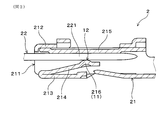
- FIG. 3 is a cross-sectional view schematically illustrating a connector terminal pair according to the first embodiment.
- 6 is a cross-sectional view schematically showing an electric contact pair of Example 2.
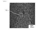
- FIG. In an experimental example, it is the photograph which looked at the top part of the projection part in sample 2 (Rh plating film) after a sliding friction test from the upper part. In an experimental example, it is the photograph which looked at the top part of the projection part in sample 3 (Ag plating film) after a sliding friction test from the upper part.
- the first plating film is laminated on the first conductive base material
- the second plating film is laminated on the second conductive base material
- the first conductive base material and the first conductive base material Two conductive base materials can be made of copper or copper alloy, or aluminum or aluminum alloy.
- an electrical contact pair suitable for a connector terminal pair using copper or a copper alloy, or aluminum or an aluminum alloy as a conductive base material can be obtained.
- the first plating film may be disposed above the first conductive base material, and the second plating film may be disposed above the second conductive base material. Therefore, the first plating film may not be in contact with the first conductive base material or may be in contact with the first conductive base material. In the former case, another plating film may be interposed between the first conductive base material and the first plating film as necessary. Similarly, the second plating film may not be in contact with the second conductive base material or may be in contact with the second conductive base material. In the former case, another plating film may be interposed between the second conductive base material and the second plating film as necessary.
- the electrical contact pair may have a base plating film made of Ni or Ni alloy below the first plating film and / or below the second plating film.
- the base plating film made of Ni or Ni alloy has high heat resistance. Therefore, in this case, even when the electrical contact pair is exposed to a high temperature environment, the oxidation diffuses from below the underlying plating film toward the surface of the first plating film or the second plating film.
- An object forming element for example, a Cu component of a conductive base material used for a connector terminal pair
- the first electrical contact may have a configuration in which a base plating layer and a first plating film are laminated in this order on the surface of the first conductive base material as necessary. it can.
- the second electrical contact can be specifically configured such that a base plating layer and a second plating film are laminated in this order on the surface of the second conductive base material as necessary.
- the thickness of the second plating film can be made thinner than the thickness of the first plating film. In this case, the basis weight of the second plating film is reduced, and there are advantages such as cost reduction.
- the friction coefficient between the first plating film and the second plating film is preferably 1/2 or less of the friction coefficient between the Ag plating films. In this case, it becomes easy to obtain an electrical contact pair having high wear resistance.
- the friction coefficient between the Ag plating films is such that the first plating film in the first electric contact is an Ag plating film, and the second plating film in the second electric contact is the same Ag plating film as described above. It can be measured using pairs. A method for measuring the friction coefficient will be described later.
- the first electrical contact has a protruding shape
- the second electrical contact has a plate shape that is in electrical contact with the top of the protruding first electrical contact. be able to.
- the second electrical contact has a projecting shape
- the first electrical contact has a plate shape that is in electrical contact with the top of the projecting second electrical contact. Can do.
- the first terminal can have a female terminal shape having a protrusion
- the second terminal has a male terminal shape having a plate-like portion that contacts the top of the protrusion. Can do.
- the second terminal can have a female terminal shape having a protrusion
- the first terminal can have a male terminal shape having a plate-like portion in contact with the top of the protrusion.
- Example 1 The electrical contact pair and connector terminal pair of Example 1 will be described with reference to FIGS.
- the electrical contact pair 1 of this example includes a first electrical contact 11 and a second electrical contact 12 that is in electrical contact with the first electrical contact 11.
- the first electrical contact 11 has a first plating film 111 made of Ag or an Ag alloy on the outermost surface.
- the second electrical contact 12 has a second plating film 121 made of Rh or Rh alloy on the outermost surface. This will be described in detail below.
- the first electrical contact 11 has a protruding shape.
- the second electrical contact 12 has a plate shape that is in electrical contact with the top of the protruding first electrical contact 11. More specifically, the first electrical contact 11 includes a protruding first conductive base material 112, a base plating film 13 laminated on the surface of the first conductive base material 112, and a surface of the base plating film 13. And a first plating film 111 laminated on the substrate.
- the second electrical contact 12 is a plate-shaped second conductive base material 122, a base plating film 13 stacked on the surface of the second conductive base material 122, and a base plating film 13. A second plating film 121.
- the first conductive base material 112 and the second conductive base material 122 are made of copper or a copper alloy.
- the base plating film 13 is made of Ni or Ni alloy.
- the thickness of the first conductive base material 112 is 250 ⁇ m.
- the thickness of the second conductive base material 122 is 250 ⁇ m.
- the thickness of the base plating film 13 formed on the surface of the first conductive base material 112 is 1 ⁇ m.
- the thickness of the base plating film 13 formed on the surface of the second conductive base material 122 is 1 ⁇ m.
- the thickness of the first plating film 111 is 5 ⁇ m.
- the thickness of the second plating film 121 is 0.3 ⁇ m.
- the connector terminal pair 2 of this example has a first terminal 21 and a second terminal 22.
- the first terminal 21 has the first electrical contact 11 described above.
- the second terminal 22 has the second electrical contact 12 described above. The details will be described below.
- the connector terminal pair 2 is used for an automobile wire harness (not shown). More specifically, the connector terminal pair 2 is applied to a power supply line through which a large current flows in an automobile.
- the first terminal 21 is a female terminal.
- the second terminal 22 is a male terminal.
- the first terminal 21 has a cylindrical portion 212 having an insertion port 211 opened at the front end.
- the second terminal 22 has a plate-like portion 221 for insertion into the insertion port 211 of the first terminal 21.
- the elastic contact piece 214 is for applying an upward force to the plate-like portion 221 of the inserted second terminal 22.
- the plate-like portion 221 of the second terminal 22 is pressed against the inner surface of the ceiling plate 215 of the tubular portion 212 by the elastic contact piece 214. As a result, the plate-like portion 221 of the second terminal 22 is held between the elastic contact piece 214 and the inner surface of the ceiling plate 215 in a compressed state.
- a protrusion 216 is formed on the elastic contact piece 214.
- the protrusion 216 is formed by causing the elastic contact piece 214 to swell in a hemispherical shape from the back side to the surface.
- the protrusion 216 of the elastic contact piece 214 is the first electrical contact 11.
- a portion that contacts the top portion of the protruding portion 216 and its peripheral portion serve as the second electrical contact 12.
- the portion other than the elastic contact piece 214 including the first electrical contact 11 in the first terminal 21 is a base plating made of Ni or a Ni plating alloy film on the surface of a conductive base material made of copper or a copper alloy.
- the film is covered, and the surface of the base plating film is covered with a Sn or Sn alloy plating film.
- the conductive base material constituting the first terminal 21 is continuous with the first conductive base material 112 of the first electrical contact 11.
- a portion (not shown) other than the plate-like portion 221 including the second electrical contact 12 in the second terminal 22 is a base plating made of Ni or a Ni plating alloy film on the surface of a conductive base material made of copper or a copper alloy.
- the film is covered, and the surface of the base plating film is covered with a Sn or Sn alloy plating film.
- the conductive base material constituting the second terminal 22 is continuous with the second conductive base material 122 of the second electrical contact 12.
- the electrical contact pair 1 of this example electrically connects the first plating film 111 of the first electrical contact 11 made of Ag or Ag alloy and the second plating film 121 of the second electrical contact 12 made of Rh or Rh alloy. Make contact. Ag and Rh have relatively high conductivity. Therefore, the electrical contact pair 1 of this example can achieve a low contact resistance.
- the electrical contact pair 1 in this example does not contact between the Ag plating films. Ag and Rh are difficult to make an alloy. Therefore, the electrical contact pair 1 of the present example does not cause severe adhesion as seen in the electrical contact pair that electrically contacts the Ag plating films. Therefore, the electrical contact pair 1 of this example can reduce wear due to adhesion between the first plating film 111 and the second plating film 121. Furthermore, Rh is harder than Ag. Therefore, wear can be reduced also by this. Therefore, the electrical contact pair 1 of this example can exhibit high wear resistance due to the combination of two effects of the optimal combination of plating film materials and the selection of relatively hard Rh.
- the electrical contact pair 1 of this example is formed by laminating a plurality of plating films as in the prior art in order to form the outermost plating films 111 and 121 in the respective electrical contacts 11 and 12, There is no need to deposit carbon particles in the plating film, and normal plating is sufficient. Therefore, the electrical contact pair 1 of this example can simplify the plating process at the time of manufacture, and can also make the plating rate relatively fast. Therefore, the electrical contact pair 1 of this example has good manufacturability.
- the first electrical contact 11 included in the first terminal 21 and the second electrical contact 12 included in the second terminal 22 constitute the electrical contact pair 1 of this example. Can be configured.
- Example 2 The electrical contact pair and connector terminal pair of Example 2 will be described with reference to FIG.
- the second electrical contact 12 has a protruding shape.
- the first electrical contact 11 has a plate shape that is in electrical contact with the top of the protruding second electrical contact 12.
- the second electrical contact 12 includes a protruding second conductive base material 122, a base plating film 13 laminated on the surface of the second conductive base material 122, and a surface of the base plating film 13. And a second plating film 121 laminated on the substrate.
- the first electrical contact 11 is a plate-shaped first conductive base material 112, a base plating film 13 stacked on the surface of the first conductive base material 112, and a base plating film 13.
- the first plating film 111 is included.
- the description of the electrical contact pair 1 of Example 1 is applied mutatis mutandis.
- the first terminal is a male terminal and the second terminal is a female terminal. That is, the connector terminal pair of this example has the male and female configurations opposite to those of the connector terminal pair of the first embodiment. Therefore, in this example, the protrusion of the elastic contact piece is the second electrical contact. Moreover, the part which contacts the top part of a projection part among the plate-shaped parts of a 1st terminal, and its peripheral part are made into a 1st electrical contact. For the other configurations, the description of the connector terminal pair of Example 1 is applied mutatis mutandis.
- the electrical contact pair and connector terminal pair of this example can also exhibit the same effects as the electrical contact pair and connector terminal pair of Example 1.
- Example preparation- An Ni plating film having a thickness of 1 ⁇ m was formed as a base plating film on the surface of a clean copper plate by an electrolytic plating method. Next, an Ag plating film having a thickness of 5 ⁇ m was formed on the surface of the Ni plating film by electrolytic plating. Thereby, Sample 1 was obtained.
- a 1 ⁇ m thick Ni plating film was formed as a base plating film on the surface of a clean copper plate by an electrolytic plating method.
- an Rh plating film having a thickness of 0.3 ⁇ m was formed on the surface of the Ni plating film by electrolytic plating.
- a substantially hemispherical protrusion was formed by bulging a part of the copper plate from the back side to the front side so as to have a curvature radius of 3 mm. As a result, Sample 2 was obtained.
- a 1 ⁇ m thick Ni plating film was formed as a base plating film on the surface of a clean copper plate by an electrolytic plating method.
- an Ag plating film having a thickness of 5 ⁇ m was formed on the surface of the Ni plating film by electrolytic plating.
- a substantially hemispherical protrusion was formed by bulging a part of the copper plate from the back side to the front side so as to have a curvature radius of 3 mm. As a result, Sample 3 was obtained.
- the dynamic friction force acting on the contact portions of both samples was measured using a load cell.
- a value obtained by dividing the dynamic friction force by the load was defined as a friction coefficient.
- the contact resistance and the friction coefficient were calculated from the average value for each sliding cycle in order to eliminate the influence of noise.
- the contact resistance of the pair consisting of Sample 1 and Sample 2 was 0.3 to 0.4 m ⁇ , and the friction coefficient was 0.3 to 0.4.
- the contact resistance of the pair consisting of Sample 1 and Sample 3 was 0.2 to 0.3 m ⁇ , and the friction coefficient was about 1.0.
- a pair consisting of a plate-like sample 1 having an Ag plating film on the outermost surface and a sample 3 having a projection having an Ag plating film on the outermost surface is subjected to Ag plating by sliding.
- Y1 is an exposed undercoat film.
- Y2 is the part which rose by the excavation by the adhesion of Ag plating films.
- a pair consisting of a plate-like sample 1 having an Ag plating film on the outermost surface and a sample 2 having a protrusion having an Rh plating film on the outermost surface is a sliding
- the scar (Y3 part) formed by rubbing by was observed.
- the underlying plating film was not exposed at this portion.
- the abrasion by adhesion with Ag plating film and Rh plating film was not seen.
- the first electrical contact having the first plating film made of Ag or Ag alloy on the outermost surface and the second electric contact having the second plating film made of Rh or Rh alloy on the outermost surface are combined for electric By configuring the contact pair, it can be said that an electrical contact pair having low contact resistance and high wear resistance can be obtained.
- the first plating film and the second plating film can be formed relatively easily by single layer plating. Therefore, it can be said that the electrical contact pair is excellent in manufacturability.
Landscapes
- Chemical & Material Sciences (AREA)
- Engineering & Computer Science (AREA)
- Materials Engineering (AREA)
- Metallurgy (AREA)
- Organic Chemistry (AREA)
- Mechanical Engineering (AREA)
- Chemical Kinetics & Catalysis (AREA)
- Electrochemistry (AREA)
- Electroplating Methods And Accessories (AREA)
- Contacts (AREA)
Abstract
電気接点対(1)は、第1電気接点(11)と、第1電気接点(11)に電気的に接触させる第2電気接点(12)とを有する。第1電気接点(11)は、最表面にAgまたはAg合金からなる第1めっき膜(111)を有しており、第2電気接点(12)は、最表面にRhまたはRh合金からなる第2めっき膜(121)を有している。第1めっき膜(111)は、第1導電性母材(112)上に積層されており、第2めっき膜(121)は、第2導電性母材(122)上に積層されており、第1導電性母材(112)および第2導電性母材(122)は、銅または銅合金、あるいは、アルミニウムまたはアルミニウム合金からなる構成とすることができる。コネクタ用端子対(2)は、第1電気接点(11)を有する第1端子(21)と、第2電気接点(12)を有する第2端子(22)とを有している。
Description
本発明は、電気接点対およびコネクタ用端子対に関する。
近年、ハイブリッド自動車や電気自動車等の普及に伴い、モーター等へ電力を供給する電力供給線等に大電流用のコネクタ用端子が使用されるようになっている。この種のコネクタ用端子同士を嵌合させてコネクタ用端子対を構成する場合、各コネクタ用端子の電気接点には、通常、接触抵抗の低いAgめっき膜が用いられる。
例えば、特許文献1には、端子を形成するためのCuまたはCu合金よりなる母材と、母材表面を被覆するAg-Sn合金めっき膜と、Ag-Sn合金めっき膜を被覆し、最表面に露出するAgめっき膜とを有するコネクタ用端子が開示されている。
他にも、特許文献2には、Agめっき膜中に一定量の炭素粒子を取り込んだ複合めっき膜を有する電気接点が開示されている。
しかしながら、従来技術は、以下の点で改善の余地がある。すなわち、Agは、比較的高い導電性を有する。そのため、Agめっき膜同士を電気的に接触させる構成の電気接点対は、接触抵抗を低くすることができる。しかしながら、Agは、比較的軟質で凝着しやすい金属である。そのため、当該電気接点対は、Agめっき膜同士の凝着による摩耗を生じやすく、耐摩耗性に劣る。特に、電気接点対に摺動による摩擦が作用する場合に、上記凝着による摩耗が顕著になる。
また、Agめっき膜の下に比較的硬いAg-Sn合金めっき膜を設けた電気接点対は、めっき膜の硬度上昇により摩擦係数を小さくすることが可能である。そのため、当該電気接点対は、低摩擦化により耐摩耗性の向上を図ることができる。しかしながら、当該電気接点対は、上記と同様に、Agめっき膜同士を電気的に接触させているため、Agめっき膜同士の凝着による摩耗を防ぐことが難しい。また、Ag-Sn合金めっき膜の上にAgめっき膜を形成するために、何層ものめっき膜を積層し、リフローする工程が必要になる。そのため、製造性が悪い。
また、炭素粒子を取り込んだ複合めっき膜を用いた電気接点対は、摩耗によって炭素粒子が露出した際に、接触抵抗が上昇するおそれがある。また、めっき膜中に炭素粒子を十分に取り込ませる必要があるため、めっき速度が遅くなり、製造性に劣ることが懸念される。
本発明は、上記背景に鑑みてなされたものであり、低接触抵抗であり、高い耐摩耗性を有しており、製造性の良好な電気接点対、また、これを用いたコネクタ用端子対を提供しようとするものである。
本発明の一態様は、第1電気接点と、該第1電気接点に電気的に接触させる第2電気接点とを有する電気接点対であって、
上記第1電気接点は、最表面にAgまたはAg合金からなる第1めっき膜を有しており、上記第2電気接点は、最表面にRhまたはRh合金からなる第2めっき膜を有していることを特徴とする電気接点対にある。
上記第1電気接点は、最表面にAgまたはAg合金からなる第1めっき膜を有しており、上記第2電気接点は、最表面にRhまたはRh合金からなる第2めっき膜を有していることを特徴とする電気接点対にある。
本発明の他の態様は、上記電気接点対を有するコネクタ用端子対であって、
上記第1電気接点を有する第1端子と、上記第2電気接点を有する第2端子とを有することを特徴とするコネクタ用端子対にある。
上記第1電気接点を有する第1端子と、上記第2電気接点を有する第2端子とを有することを特徴とするコネクタ用端子対にある。
上記電気接点対は、AgまたはAg合金からなる第1電気接点の第1めっき膜と、RhまたはRh合金からなる第2電気接点の第2めっき膜とを電気的に接触させる。Ag、Rhは、比較的高い導電性を有する。そのため、上記電気接点対は、低接触抵抗を実現することができる。
また、上記電気接点対は、Agめっき膜同士の接触にならない。また、AgとRhとは合金をつくり難い。そのため、上記電気接点対は、Agめっき膜同士を電気的に接触させる電気接点対に見られるような激しい凝着を生じることがない。それ故、上記電気接点対は、第1めっき膜と第2めっき膜との凝着による摩耗を低減することができる。さらに、Rhは、Agよりも硬質である。そのため、これによっても、摩耗を低減することができる。したがって、上記電気接点対は、めっき膜材料の最適な組み合わせと比較的硬いRhの選択とによる2つの効果が相まって、高い耐摩耗性を発揮することができる。
また、上記電気接点対は、各電気接点における最表面のめっき膜を形成するために、従来技術のように複数のめっき膜を積層してリフロー処理したり、めっき膜中に炭素粒子を析出させたりする必要がなく、通常のめっきで済む。そのため、上記電気接点対は、製造時におけるめっき工程が簡略化できるとともに、めっき速度も比較的早くすることができる。それ故、上記電気接点対は、良好な製造性を有している。
よって、本発明によれば、低接触抵抗であり、高い耐摩耗性を有しており、製造性の良好な電気接点対を得ることができる。
また、上記コネクタ用端子対によれば、第1端子が有する上記第1電気接点と、第2端子が有する上記第2電気接点とにより、上記電気接点対を構成することができる。
よって、本発明によれば、低接触抵抗であり、高い耐摩耗性を有しており、製造性の良好な電気接点対を有するコネクタ用端子対を提供することができる。
上記電気接点対は、第1めっき膜が第1導電性母材上に積層されており、第2めっき膜が第2導電性母材上に積層されており、第1導電性母材および第2導電性母材が、銅または銅合金、あるいは、アルミニウムまたはアルミニウム合金からなる構成とすることができる。
この場合には、銅または銅合金、あるいは、アルミニウムまたはアルミニウム合金を導電性母材とするコネクタ用端子対に好適な電気接点対が得られる。
なお、第1めっき膜は第1導電性母材の上方、第2めっき膜は第2導電性母材の上方に配置されておればよい。したがって、第1めっき膜は、第1導電性母材に接していなくてもよいし、第1導電性母材に接していてもよい。前者の場合には、第1導電性母材と第1めっき膜との間に、必要に応じて、他のめっき膜が介在していてもよい。同様に、第2めっき膜は、第2導電性母材に接していなくてもよいし、第2導電性母材に接していてもよい。前者の場合には、第2導電性母材と第2めっき膜との間に、必要に応じて、他のめっき膜が介在していてもよい。
上記電気接点対は、第1めっき膜の下方、および/または、第2めっき膜の下方に、NiまたはNi合金からなる下地めっき膜を有している構成とすることができる。
NiまたはNi合金からなる下地めっき膜は、高い耐熱性を有する。そのため、この場合には、上記電気接点対が高温環境下に曝された場合であっても、下地めっき膜の下方から第1めっき膜や第2めっき膜の表面に向かって拡散してくる酸化物形成元素(例えば、コネクタ用端子対に用いられる導電性母材のCu成分等)を、下地めっき膜にて遮断することができる。そのため、第1めっき膜や第2めっき膜の表面に絶縁性の酸化物が形成され難くなり、接触抵抗の増大を抑制しやすくなる。
上記電気接点対において、第1電気接点は、具体的には、第1導電性母材の表面に、必要に応じて下地めっき層、第1めっき膜がこの順に積層された構成とすることができる。また、第2電気接点は、具体的には、第2導電性母材の表面に、必要に応じて下地めっき層、第2めっき膜がこの順に積層された構成とすることができる。
上記電気接点対において、第2めっき膜の厚みは、第1めっき膜の厚みよりも薄くされている構成とすることができる。この場合には、第2めっき膜の目付量が低減され、コスト低減などの利点がある。
上記電気接点対において、第1めっき膜と第2めっき膜との間の摩擦係数は、Agめっき膜同士間の摩擦係数の1/2以下であることが好ましい。この場合には、高い耐摩耗性を有する電気接点対を得やすくなる。
なお、Agめっき膜同士間の摩擦係数は、第1電気接点における第1めっき膜をAgめっき膜とするとともに、第2電気接点における第2めっき膜を上記と同じAgめっき膜として構成した電気接点対を用いて測定することができる。摩擦係数の測定方法は、後述する。
上記電気接点対において、第1電気接点は、突起状の形状を有しており、第2電気接点は、突起状の第1電気接点の頂部と電気的に接触する板形状を有する構成とすることができる。また他にも、第2電気接点は、突起状の形状を有しており、第1電気接点は、突起状の第2電気接点の頂部と電気的に接触する板形状を有する構成とすることができる。
上記コネクタ用端子対において、第1端子は、突起部を有するメス型端子形状を呈することができ、第2端子は、突起部の頂部と接触する板状部を有するオス型端子形状を呈することができる。また、第2端子は、突起部を有するメス型端子形状を呈することができ、第1端子は、突起部の頂部と接触する板状部を有するオス型端子形状を呈することができる。
なお、上述した各構成は、上述した各作用効果等を得るなどのために必要に応じて任意に組み合わせることができる。
以下、実施例の電気接点対およびコネクタ用端子対について、図面を用いて説明する。なお、同一部材については同一の符号を用いて説明する。
(実施例1)
実施例1の電気接点対およびコネクタ用端子対について、図1、図2を用いて説明する。図1に示されるように、本例の電気接点対1は、第1電気接点11と、第1電気接点11に電気的に接触させる第2電気接点12とを有している。第1電気接点11は、最表面にAgまたはAg合金からなる第1めっき膜111を有している。第2電気接点12は、最表面にRhまたはRh合金からなる第2めっき膜121を有している。以下、これを詳説する。
実施例1の電気接点対およびコネクタ用端子対について、図1、図2を用いて説明する。図1に示されるように、本例の電気接点対1は、第1電気接点11と、第1電気接点11に電気的に接触させる第2電気接点12とを有している。第1電気接点11は、最表面にAgまたはAg合金からなる第1めっき膜111を有している。第2電気接点12は、最表面にRhまたはRh合金からなる第2めっき膜121を有している。以下、これを詳説する。
本例では、具体的には、第1電気接点11は、突起状の形状を有している。また、第2電気接点12は、突起状の第1電気接点11の頂部と電気的に接触する板形状を有している。より具体的には、第1電気接点11は、突起状の第1導電性母材112と、第1導電性母材112の表面に積層された下地めっき膜13と、下地めっき膜13の表面に積層された第1めっき膜111とを有している。また、第2電気接点12は、板形状の第2導電性母材122と、第2導電性母材122の表面に積層された下地めっき膜13と、下地めっき膜13の表面に積層された第2めっき膜121とを有している。
本例では、第1導電性母材112および第2導電性母材122は、銅または銅合金からなる。下地めっき膜13は、NiまたはNi合金からなる。第1導電性母材112の厚みは、250μmである。第2導電性母材122の厚みは、250μmである。第1導電性母材112の表面に形成されている下地めっき膜13の厚みは、1μmである。第2導電性母材122の表面に形成されている下地めっき膜13の厚みは、1μmである。第1めっき膜111の厚みは、5μmである。第2めっき膜121の厚みは、0.3μmである。
次に、図2に示されるように、本例のコネクタ用端子対2は、第1端子21と、第2端子22とを有している。第1端子21は、上記の第1電気接点11を有している。第2端子22は、上記の第2電気接点12を有している。以下、詳説する。
本例において、コネクタ用端子対2は、自動車用ワイヤーハーネス(不図示)に用いられるものである。より具体的には、コネクタ用端子対2は、自動車において大電流が流れる電力供給線に適用される。第1端子21は、具体的には、メス型端子である。第2端子22は、具体的には、オス型端子である。
第1端子21は、前端に挿入口211が開口した筒状部212を有している。一方、第2端子22は、第1端子21の挿入口211内に挿入させるための板状部221を有している。第1端子21の筒状部212の内部には、底面板213が内側後方へ折り返されて形成された弾性接触片214が設けられている。弾性接触片214は、挿入された第2端子22の板状部221に上向きの力を加えるためのものである。第2端子22の板状部221は、弾性接触片214によって筒状部212の天井板215の内側面に押し付けられる。これにより、第2端子22の板状部221が弾性接触片214と天井板215の内側面との間に挟圧状態で保持される。
弾性接触片214には、突起部216が形成されている。突起部216は、弾性接触片214を裏側から表面に向かって半球状に膨出させることによって形成されている。本例では、弾性接触片214の突起部216が第1電気接点11とされる。また、第2端子22の板状部221のうち、突起部216の頂部と接触する部分とその周辺部分が、第2電気接点12とされる。
なお、本例では、第1端子21における第1電気接点11を含む弾性接触片214以外の部分は、銅または銅合金からなる導電性母材の表面にNiまたはNiめっき合金膜からなる下地めっき膜が被覆され、下地めっき膜の表面にSnまたはSn合金めっき膜が被覆されている。なお、第1端子21を構成する導電性母材は、第1電気接点11の第1導電性母材112と連続している。また、第2端子22における第2電気接点12を含む板状部221以外の部分(不図示)は、銅または銅合金からなる導電性母材の表面にNiまたはNiめっき合金膜からなる下地めっき膜が被覆され、下地めっき膜の表面にSnまたはSn合金めっき膜が被覆されている。なお、第2端子22を構成する導電性母材は、第2電気接点12の第2導電性母材122と連続している。
次に、本例の電気接点対およびコネクタ用端子対の作用効果について説明する。
本例の電気接点対1は、AgまたはAg合金からなる第1電気接点11の第1めっき膜111と、RhまたはRh合金からなる第2電気接点12の第2めっき膜121とを電気的に接触させる。Ag、Rhは、比較的高い導電性を有する。そのため、本例の電気接点対1は、低接触抵抗を実現することができる。
また、本例の電気接点対1は、Agめっき膜同士の接触にならない。また、AgとRhとは合金をつくり難い。そのため、本例の電気接点対1は、Agめっき膜同士を電気的に接触させる電気接点対に見られるような激しい凝着を生じることがない。それ故、本例の電気接点対1は、第1めっき膜111と第2めっき膜121との凝着による摩耗を低減することができる。さらに、Rhは、Agよりも硬質である。そのため、これによっても、摩耗を低減することができる。したがって、本例の電気接点対1は、めっき膜材料の最適な組み合わせと比較的硬いRhの選択とによる2つの効果が相まって、高い耐摩耗性を発揮することができる。
また、本例の電気接点対1は、各電気接点11、12における最表面のめっき膜111、121を形成するために、従来技術のように複数のめっき膜を積層してリフロー処理したり、めっき膜中に炭素粒子を析出させたりする必要がなく、通常のめっきで済む。そのため、本例の電気接点対1は、製造時におけるめっき工程が簡略化できるとともに、めっき速度も比較的早くすることができる。それ故、本例の電気接点対1は、良好な製造性を有している。
また、本例のコネクタ用端子対2によれば、第1端子21が有する上記第1電気接点11と、第2端子22が有する上記第2電気接点12とにより、本例の電気接点対1を構成することができる。
(実施例2)
実施例2の電気接点対およびコネクタ用端子対について、図3を用いて説明する。図3に示されるように、本例の電気接点対1において、第2電気接点12は、突起状の形状を有している。また、第1電気接点11は、突起状の第2電気接点12の頂部と電気的に接触する板形状を有している。より具体的には、第2電気接点12は、突起状の第2導電性母材122と、第2導電性母材122の表面に積層された下地めっき膜13と、下地めっき膜13の表面に積層された第2めっき膜121とを有している。また、第1電気接点11は、板形状の第1導電性母材112と、第1導電性母材112の表面に積層された下地めっき膜13と、下地めっき膜13の表面に積層された第1めっき膜111とを有している。その他の構成については、実施例1の電気接点対1の記載が準用される。
実施例2の電気接点対およびコネクタ用端子対について、図3を用いて説明する。図3に示されるように、本例の電気接点対1において、第2電気接点12は、突起状の形状を有している。また、第1電気接点11は、突起状の第2電気接点12の頂部と電気的に接触する板形状を有している。より具体的には、第2電気接点12は、突起状の第2導電性母材122と、第2導電性母材122の表面に積層された下地めっき膜13と、下地めっき膜13の表面に積層された第2めっき膜121とを有している。また、第1電気接点11は、板形状の第1導電性母材112と、第1導電性母材112の表面に積層された下地めっき膜13と、下地めっき膜13の表面に積層された第1めっき膜111とを有している。その他の構成については、実施例1の電気接点対1の記載が準用される。
また、本例のコネクタ用端子対(不図示)は、第1端子がオス型端子であり、第2端子がメス型端子である。つまり、本例のコネクタ用端子対は、実施例1のコネクタ用端子対とオス、メスの構成が逆になっている。したがって、本例では、弾性接触片の突起部が第2電気接点とされる。また、第1端子の板状部のうち、突起部の頂部と接触する部分とその周辺部分が、第1電気接点とされる。その他の構成については、実施例1のコネクタ用端子対の記載が準用される。
本例の電気接点対およびコネクタ用端子対についても、実施例1の電気接点対およびコネクタ用端子対と同様の作用効果を奏することができる。
<実験例>
以下、実験例を用いてより具体的に説明する。
以下、実験例を用いてより具体的に説明する。
-試料の作製-
清浄な銅板の表面に、電解めっき法により、下地めっき膜として、厚み1μmのNiめっき膜を形成した。次いで、このNiめっき膜の表面に、電解めっき法により、厚み5μmのAgめっき膜を形成した。これにより、試料1を得た。
清浄な銅板の表面に、電解めっき法により、下地めっき膜として、厚み1μmのNiめっき膜を形成した。次いで、このNiめっき膜の表面に、電解めっき法により、厚み5μmのAgめっき膜を形成した。これにより、試料1を得た。
また、清浄な銅板の表面に、電解めっき法により、下地めっき膜として、厚み1μmのNiめっき膜を形成した。次いで、このNiめっき膜の表面に、電解めっき法により、厚み0.3μmのRhめっき膜を形成した。次いで、この銅板の一部を曲率半径3mmとなるように裏側から表側に向かって膨出させることにより、略半球状の突起部を形成した。これにより試料2を得た。
また、清浄な銅板の表面に、電解めっき法により、下地めっき膜として、厚み1μmのNiめっき膜を形成した。次いで、このNiめっき膜の表面に、電解めっき法により、厚み5μmのAgめっき膜を形成した。次いで、この銅板の一部を曲率半径3mmとなるように裏側から表側に向かって膨出させることにより、略半球状の突起部を形成した。これにより試料3を得た。
-摺動時の接触抵抗と摩擦係数の測定-
最表面にAgめっき膜を有する板状の試料1と、最表面にRhめっき膜を有する突起部を備えた試料2とを、試料1のAgめっき膜に試料2の突起部の頂部を鉛直方向に接触させた状態で保持し、ピエゾアクチュエータを用いて鉛直方向に5Nの荷重を印加しながら、10mm/min.の速度で試料2を水平方向に引張り、7mmの距離を繰り返し往復させることにより摺動させた。繰り返し摺動を行う間、両試料間の接触抵抗を四端子法により測定した。この際、開放電圧を20mV、通電電流を10mAとした。また、これと同時に、ロードセルを使用して両試料の接点部に働く動摩擦力を測定した。そして、動摩擦力を荷重で割った値を摩擦係数とした。上記摺動は、25往復にわたって行った。したがって、本試験における摺動距離は、摺動1回の距離14mm×25往復=350mmである。また、当該測定は、室温にて行った。
最表面にAgめっき膜を有する板状の試料1と、最表面にRhめっき膜を有する突起部を備えた試料2とを、試料1のAgめっき膜に試料2の突起部の頂部を鉛直方向に接触させた状態で保持し、ピエゾアクチュエータを用いて鉛直方向に5Nの荷重を印加しながら、10mm/min.の速度で試料2を水平方向に引張り、7mmの距離を繰り返し往復させることにより摺動させた。繰り返し摺動を行う間、両試料間の接触抵抗を四端子法により測定した。この際、開放電圧を20mV、通電電流を10mAとした。また、これと同時に、ロードセルを使用して両試料の接点部に働く動摩擦力を測定した。そして、動摩擦力を荷重で割った値を摩擦係数とした。上記摺動は、25往復にわたって行った。したがって、本試験における摺動距離は、摺動1回の距離14mm×25往復=350mmである。また、当該測定は、室温にて行った。
また、最表面にAgめっき膜を有する板状の試料1と、最表面にAgめっき膜を有する突起部を備えた試料3とを用いた以外は上記同様にして、摺動時の接触抵抗と摩擦係数とを測定した。
なお、上記接触抵抗、摩擦係数は、ノイズの影響を除くために摺動回数1回ごとの平均値から算出した。
上記の結果、試料1と試料2とからなる対における接触抵抗は、0.3~0.4mΩであり、摩擦係数は、0.3~0.4であった。一方、試料1と試料3とからなる対における接触抵抗は、0.2~0.3mΩであり、摩擦係数は、約1.0であった。
-摺動摩擦試験後の摩耗痕の観察-
図5に示されるように、最表面にAgめっき膜を有する板状の試料1と、最表面にAgめっき膜を有する突起部を備えた試料3とからなる対は、摺動により、Agめっき膜同士が凝着し、下地めっき膜が露出した。なお、図5中、Y1が露出した下地めっき膜である。また、Y2がAgめっき膜同士の凝着による掘り起こしによって盛り上がった部分である。
図5に示されるように、最表面にAgめっき膜を有する板状の試料1と、最表面にAgめっき膜を有する突起部を備えた試料3とからなる対は、摺動により、Agめっき膜同士が凝着し、下地めっき膜が露出した。なお、図5中、Y1が露出した下地めっき膜である。また、Y2がAgめっき膜同士の凝着による掘り起こしによって盛り上がった部分である。
これに対し、図4に示されるように、最表面にAgめっき膜を有する板状の試料1と、最表面にRhめっき膜を有する突起部を備えた試料2とからなる対は、摺動によるこすれによって形成された傷跡(Y3の部分)が見られた。しかしながら、この部分で下地めっき膜は露出していなかった。また、Agめっき膜とRhめっき膜との凝着による摩耗は見られなかった。
上記の結果から、最表面にAgまたはAg合金からなる第1めっき膜を有する第1電気接点と、最表面にRhまたはRh合金からなる第2めっき膜を有する第2電気接点とを組み合わせて電気接点対を構成することにより、低接触抵抗であり、高い耐摩耗性を有する電気接点対を得ることができるといえる。また、第1めっき膜、第2めっき膜は、単層めっきで比較的簡単に形成することができる。そのため、電気接点対の製造性にも優れているといえる。
以上、本発明の実施例について詳細に説明したが、本発明は上記実施例に限定されるものではなく、本発明の趣旨を損なわない範囲内で種々の変更が可能である。
Claims (5)
- 第1電気接点と、該第1電気接点に電気的に接触させる第2電気接点とを有する電気接点対であって、
上記第1電気接点は、最表面にAgまたはAg合金からなる第1めっき膜を有しており、上記第2電気接点は、最表面にRhまたはRh合金からなる第2めっき膜を有している、電気接点対。 - 上記第1めっき膜は、第1導電性母材上に積層されており、
上記第2めっき膜は、第2導電性母材上に積層されており、
上記第1導電性母材および上記第2導電性母材は、銅または銅合金、あるいは、アルミニウムまたはアルミニウム合金からなる、請求項1に記載の電気接点対。 - 上記第1めっき膜の下方、および/または、上記第2めっき膜の下方に、
NiまたはNi合金からなる下地めっき膜を有している、請求項1または2に記載の電気接点対。 - 上記第1めっき膜と上記第2めっき膜との間の摩擦係数は、Agめっき膜同士間の摩擦係数の1/2以下である、請求項1~3のいずれか1項に記載の電気接点対。
- 請求項1~4の何れか1項に記載の電気接点対を有するコネクタ用端子対であって、
上記第1電気接点を有する第1端子と、上記第2電気接点を有する第2端子とを有する、コネクタ用端子対。
Priority Applications (3)
| Application Number | Priority Date | Filing Date | Title |
|---|---|---|---|
| DE112015005914.8T DE112015005914B4 (de) | 2015-01-09 | 2015-12-24 | Verbindungsanschlusspaar |
| US15/541,561 US10069231B2 (en) | 2015-01-09 | 2015-12-24 | Connector terminal pair |
| CN201580069712.1A CN107112671B (zh) | 2015-01-09 | 2015-12-24 | 连接器用端子对 |
Applications Claiming Priority (2)
| Application Number | Priority Date | Filing Date | Title |
|---|---|---|---|
| JP2015-003473 | 2015-01-09 | ||
| JP2015003473A JP6332043B2 (ja) | 2015-01-09 | 2015-01-09 | コネクタ用端子対 |
Publications (1)
| Publication Number | Publication Date |
|---|---|
| WO2016111187A1 true WO2016111187A1 (ja) | 2016-07-14 |
Family
ID=56355886
Family Applications (1)
| Application Number | Title | Priority Date | Filing Date |
|---|---|---|---|
| PCT/JP2015/086125 Ceased WO2016111187A1 (ja) | 2015-01-09 | 2015-12-24 | 電気接点対およびコネクタ用端子対 |
Country Status (5)
| Country | Link |
|---|---|
| US (1) | US10069231B2 (ja) |
| JP (1) | JP6332043B2 (ja) |
| CN (1) | CN107112671B (ja) |
| DE (1) | DE112015005914B4 (ja) |
| WO (1) | WO2016111187A1 (ja) |
Families Citing this family (7)
| Publication number | Priority date | Publication date | Assignee | Title |
|---|---|---|---|---|
| JP6267404B1 (ja) * | 2017-01-30 | 2018-01-24 | Jx金属株式会社 | 表面処理めっき材、コネクタ端子、コネクタ、ffc端子、ffc、fpc及び電子部品 |
| US10186795B2 (en) * | 2017-06-15 | 2019-01-22 | Yazaki Corporation | Electrical contact member, plated terminal, terminal-attached electrical wire, and wire harness |
| JP7014617B2 (ja) | 2018-01-17 | 2022-02-01 | 富士通コンポーネント株式会社 | 電磁継電器 |
| JP2019197691A (ja) * | 2018-05-11 | 2019-11-14 | 矢崎総業株式会社 | 接点接続構造 |
| CN109687225B (zh) * | 2018-12-17 | 2020-09-11 | 新奥科技发展有限公司 | 一种真空高温环境的电连接器 |
| CN111755932B (zh) * | 2019-03-26 | 2025-01-17 | 富士康(昆山)电脑接插件有限公司 | 一种导电端子的制造方法 |
| JP7758487B2 (ja) * | 2021-07-02 | 2025-10-22 | Dowaメタルテック株式会社 | 複合材、複合材の製造方法、端子及び端子の製造方法 |
Citations (8)
| Publication number | Priority date | Publication date | Assignee | Title |
|---|---|---|---|---|
| JPS51125892A (en) * | 1975-04-22 | 1976-11-02 | Hitachi Ltd | Connecting equipment for very low- temperature electric device |
| JPS59177817A (ja) * | 1983-03-26 | 1984-10-08 | 富士通株式会社 | 電気接触子 |
| JP2004190064A (ja) * | 2002-12-09 | 2004-07-08 | Matsushita Electric Works Ltd | 金属端子の表面処理方法及び金属端子 |
| JP2006108057A (ja) * | 2004-10-08 | 2006-04-20 | Matsushita Electric Works Ltd | コネクタ接続端子 |
| JP2008095186A (ja) * | 2006-09-13 | 2008-04-24 | Furukawa Electric Co Ltd:The | 接点材用銅基析出型合金板材およびその製造方法 |
| JP2010146925A (ja) * | 2008-12-19 | 2010-07-01 | Furukawa Electric Co Ltd:The | モータ用接触子材料およびその製造方法 |
| JP2011124141A (ja) * | 2009-12-11 | 2011-06-23 | Autonetworks Technologies Ltd | 電気接点及びコネクタ端子 |
| JP2014175196A (ja) * | 2013-03-11 | 2014-09-22 | Auto Network Gijutsu Kenkyusho:Kk | コネクタ用接続端子 |
Family Cites Families (22)
| Publication number | Priority date | Publication date | Assignee | Title |
|---|---|---|---|---|
| US5476211A (en) * | 1993-11-16 | 1995-12-19 | Form Factor, Inc. | Method of manufacturing electrical contacts, using a sacrificial member |
| WO1998027620A1 (en) * | 1996-12-19 | 1998-06-25 | Ritson John D | Battery connector with conductive coating |
| TW575688B (en) * | 2001-01-19 | 2004-02-11 | Furukawa Electric Co Ltd | Metal-plated material and method for preparation thereof, and electric and electronic parts using the same |
| US6860769B2 (en) * | 2002-01-12 | 2005-03-01 | Taiwan Semiconductor Manufacturing Co., Ltd | Cathode contact pin for an electroplating process |
| US6793544B2 (en) * | 2003-02-05 | 2004-09-21 | General Motors Corporation | Corrosion resistant fuel cell terminal plates |
| JP3795898B2 (ja) * | 2003-06-20 | 2006-07-12 | アルプス電気株式会社 | 接続装置 |
| JP4806808B2 (ja) | 2005-07-05 | 2011-11-02 | Dowaメタルテック株式会社 | 複合めっき材およびその製造方法 |
| JP5128153B2 (ja) | 2006-03-17 | 2013-01-23 | 古河電気工業株式会社 | 電気接点材料及びその製造方法 |
| CN101535512A (zh) * | 2006-09-13 | 2009-09-16 | 古河电气工业株式会社 | 触点材料用铜基析出型合金板材及其制造方法 |
| US9694562B2 (en) * | 2010-03-12 | 2017-07-04 | Xtalic Corporation | Coated articles and methods |
| JP5625166B2 (ja) | 2011-01-05 | 2014-11-19 | Dowaメタルテック株式会社 | 複合めっき材およびその製造方法 |
| JP5086485B1 (ja) * | 2011-09-20 | 2012-11-28 | Jx日鉱日石金属株式会社 | 電子部品用金属材料及びその製造方法 |
| JP5284526B1 (ja) * | 2011-10-04 | 2013-09-11 | Jx日鉱日石金属株式会社 | 電子部品用金属材料及びその製造方法 |
| TWI493798B (zh) * | 2012-02-03 | 2015-07-21 | Jx日鑛日石金屬股份有限公司 | Push-in terminals and electronic parts for their use |
| JP5387742B2 (ja) | 2012-04-06 | 2014-01-15 | 株式会社オートネットワーク技術研究所 | めっき部材、コネクタ用めっき端子、めっき部材の製造方法、及びコネクタ用めっき端子の製造方法 |
| JP6029435B2 (ja) * | 2012-06-27 | 2016-11-24 | Jx金属株式会社 | 電子部品用金属材料及びその製造方法、それを用いたコネクタ端子、コネクタ及び電子部品 |
| JP6050664B2 (ja) * | 2012-06-27 | 2016-12-21 | Jx金属株式会社 | 電子部品用金属材料及びその製造方法、それを用いたコネクタ端子、コネクタ及び電子部品 |
| JP5427945B2 (ja) * | 2012-06-27 | 2014-02-26 | Jx日鉱日石金属株式会社 | 電子部品用金属材料及びその製造方法、それを用いたコネクタ端子、コネクタ及び電子部品 |
| ES2643901T3 (es) * | 2012-07-25 | 2017-11-27 | Jx Nippon Mining & Metals Corporation | Material metálico para componentes electrónicos y método de producción del mismo, y terminales de conector, conectores y componentes electrónicos que usan el mismo |
| JP5667152B2 (ja) * | 2012-09-19 | 2015-02-12 | Jx日鉱日石金属株式会社 | 表面処理めっき材およびその製造方法、並びに電子部品 |
| TWI488733B (zh) * | 2012-10-04 | 2015-06-21 | Jx日鑛日石金屬股份有限公司 | Metal material for electronic parts and manufacturing method thereof |
| JP6330689B2 (ja) * | 2015-02-19 | 2018-05-30 | 株式会社オートネットワーク技術研究所 | 電気接点対およびコネクタ用端子対 |
-
2015
- 2015-01-09 JP JP2015003473A patent/JP6332043B2/ja not_active Expired - Fee Related
- 2015-12-24 DE DE112015005914.8T patent/DE112015005914B4/de not_active Expired - Fee Related
- 2015-12-24 WO PCT/JP2015/086125 patent/WO2016111187A1/ja not_active Ceased
- 2015-12-24 CN CN201580069712.1A patent/CN107112671B/zh not_active Expired - Fee Related
- 2015-12-24 US US15/541,561 patent/US10069231B2/en active Active
Patent Citations (8)
| Publication number | Priority date | Publication date | Assignee | Title |
|---|---|---|---|---|
| JPS51125892A (en) * | 1975-04-22 | 1976-11-02 | Hitachi Ltd | Connecting equipment for very low- temperature electric device |
| JPS59177817A (ja) * | 1983-03-26 | 1984-10-08 | 富士通株式会社 | 電気接触子 |
| JP2004190064A (ja) * | 2002-12-09 | 2004-07-08 | Matsushita Electric Works Ltd | 金属端子の表面処理方法及び金属端子 |
| JP2006108057A (ja) * | 2004-10-08 | 2006-04-20 | Matsushita Electric Works Ltd | コネクタ接続端子 |
| JP2008095186A (ja) * | 2006-09-13 | 2008-04-24 | Furukawa Electric Co Ltd:The | 接点材用銅基析出型合金板材およびその製造方法 |
| JP2010146925A (ja) * | 2008-12-19 | 2010-07-01 | Furukawa Electric Co Ltd:The | モータ用接触子材料およびその製造方法 |
| JP2011124141A (ja) * | 2009-12-11 | 2011-06-23 | Autonetworks Technologies Ltd | 電気接点及びコネクタ端子 |
| JP2014175196A (ja) * | 2013-03-11 | 2014-09-22 | Auto Network Gijutsu Kenkyusho:Kk | コネクタ用接続端子 |
Also Published As
| Publication number | Publication date |
|---|---|
| JP6332043B2 (ja) | 2018-05-30 |
| DE112015005914T5 (de) | 2017-09-21 |
| US10069231B2 (en) | 2018-09-04 |
| DE112015005914B4 (de) | 2022-05-25 |
| US20170352972A1 (en) | 2017-12-07 |
| CN107112671B (zh) | 2019-09-20 |
| CN107112671A (zh) | 2017-08-29 |
| JP2016129119A (ja) | 2016-07-14 |
Similar Documents
| Publication | Publication Date | Title |
|---|---|---|
| JP6332043B2 (ja) | コネクタ用端子対 | |
| JP5696811B2 (ja) | コネクタ用めっき端子および端子対 | |
| US9692162B2 (en) | Electric contact and connector terminal pair | |
| US20150236439A1 (en) | Plated terminal for connector, and terminal pair | |
| US10367288B1 (en) | Electric contact and connector terminal pair | |
| JPWO2015151959A1 (ja) | 端子対及び端子対を備えたコネクタ対 | |
| WO2015045856A1 (ja) | コネクタ用電気接点材料及びその製造方法 | |
| US10418736B2 (en) | Metal plate for terminal, terminal, and terminal pair | |
| JP2012237055A (ja) | コネクタ用電気接点材料とその製造方法およびコネクタ用電気接点 | |
| WO2015108004A1 (ja) | コネクタ用電気接点材料及びその製造方法 | |
| JP6377599B2 (ja) | 端子対およびコネクタ | |
| JP6330689B2 (ja) | 電気接点対およびコネクタ用端子対 | |
| JP5261278B2 (ja) | コネクタおよびコネクタ用金属材料 | |
| US10804633B2 (en) | Electrical contact point, connector terminal pair and connector pair | |
| US10804632B2 (en) | Connection terminal and method for producing connection terminal | |
| JP2015059260A (ja) | コネクタ用電気接点材料及びその製造方法 | |
| WO2016147894A1 (ja) | 電気接点対およびコネクタ用端子対 | |
| JP6282205B2 (ja) | 電気接点材料の製造方法 |
Legal Events
| Date | Code | Title | Description |
|---|---|---|---|
| 121 | Ep: the epo has been informed by wipo that ep was designated in this application |
Ref document number: 15877060 Country of ref document: EP Kind code of ref document: A1 |
|
| WWE | Wipo information: entry into national phase |
Ref document number: 15541561 Country of ref document: US |
|
| WWE | Wipo information: entry into national phase |
Ref document number: 112015005914 Country of ref document: DE |
|
| 122 | Ep: pct application non-entry in european phase |
Ref document number: 15877060 Country of ref document: EP Kind code of ref document: A1 |