WO2016103328A1 - スイッチング装置、モータ駆動装置、電力変換装置およびスイッチング方法 - Google Patents
スイッチング装置、モータ駆動装置、電力変換装置およびスイッチング方法 Download PDFInfo
- Publication number
- WO2016103328A1 WO2016103328A1 PCT/JP2014/083942 JP2014083942W WO2016103328A1 WO 2016103328 A1 WO2016103328 A1 WO 2016103328A1 JP 2014083942 W JP2014083942 W JP 2014083942W WO 2016103328 A1 WO2016103328 A1 WO 2016103328A1
- Authority
- WO
- WIPO (PCT)
- Prior art keywords
- switching
- switching element
- control
- circuit unit
- igbt
- Prior art date
Links
Images


Classifications
-
- H—ELECTRICITY
- H02—GENERATION; CONVERSION OR DISTRIBUTION OF ELECTRIC POWER
- H02M—APPARATUS FOR CONVERSION BETWEEN AC AND AC, BETWEEN AC AND DC, OR BETWEEN DC AND DC, AND FOR USE WITH MAINS OR SIMILAR POWER SUPPLY SYSTEMS; CONVERSION OF DC OR AC INPUT POWER INTO SURGE OUTPUT POWER; CONTROL OR REGULATION THEREOF
- H02M7/00—Conversion of ac power input into dc power output; Conversion of dc power input into ac power output
- H02M7/42—Conversion of dc power input into ac power output without possibility of reversal
- H02M7/44—Conversion of dc power input into ac power output without possibility of reversal by static converters
- H02M7/48—Conversion of dc power input into ac power output without possibility of reversal by static converters using discharge tubes with control electrode or semiconductor devices with control electrode
-
- H—ELECTRICITY
- H03—ELECTRONIC CIRCUITRY
- H03K—PULSE TECHNIQUE
- H03K17/00—Electronic switching or gating, i.e. not by contact-making and –breaking
- H03K17/04—Modifications for accelerating switching
- H03K17/041—Modifications for accelerating switching without feedback from the output circuit to the control circuit
- H03K17/0412—Modifications for accelerating switching without feedback from the output circuit to the control circuit by measures taken in the control circuit
-
- H—ELECTRICITY
- H03—ELECTRONIC CIRCUITRY
- H03K—PULSE TECHNIQUE
- H03K17/00—Electronic switching or gating, i.e. not by contact-making and –breaking
- H03K17/12—Modifications for increasing the maximum permissible switched current
- H03K17/122—Modifications for increasing the maximum permissible switched current in field-effect transistor switches
-
- H—ELECTRICITY
- H03—ELECTRONIC CIRCUITRY
- H03K—PULSE TECHNIQUE
- H03K17/00—Electronic switching or gating, i.e. not by contact-making and –breaking
- H03K17/12—Modifications for increasing the maximum permissible switched current
- H03K17/127—Modifications for increasing the maximum permissible switched current in composite switches
-
- H—ELECTRICITY
- H02—GENERATION; CONVERSION OR DISTRIBUTION OF ELECTRIC POWER
- H02M—APPARATUS FOR CONVERSION BETWEEN AC AND AC, BETWEEN AC AND DC, OR BETWEEN DC AND DC, AND FOR USE WITH MAINS OR SIMILAR POWER SUPPLY SYSTEMS; CONVERSION OF DC OR AC INPUT POWER INTO SURGE OUTPUT POWER; CONTROL OR REGULATION THEREOF
- H02M1/00—Details of apparatus for conversion
- H02M1/0048—Circuits or arrangements for reducing losses
-
- H—ELECTRICITY
- H02—GENERATION; CONVERSION OR DISTRIBUTION OF ELECTRIC POWER
- H02M—APPARATUS FOR CONVERSION BETWEEN AC AND AC, BETWEEN AC AND DC, OR BETWEEN DC AND DC, AND FOR USE WITH MAINS OR SIMILAR POWER SUPPLY SYSTEMS; CONVERSION OF DC OR AC INPUT POWER INTO SURGE OUTPUT POWER; CONTROL OR REGULATION THEREOF
- H02M1/00—Details of apparatus for conversion
- H02M1/08—Circuits specially adapted for the generation of control voltages for semiconductor devices incorporated in static converters
-
- H—ELECTRICITY
- H03—ELECTRONIC CIRCUITRY
- H03K—PULSE TECHNIQUE
- H03K2217/00—Indexing scheme related to electronic switching or gating, i.e. not by contact-making or -breaking covered by H03K17/00
- H03K2217/0036—Means reducing energy consumption
-
- Y—GENERAL TAGGING OF NEW TECHNOLOGICAL DEVELOPMENTS; GENERAL TAGGING OF CROSS-SECTIONAL TECHNOLOGIES SPANNING OVER SEVERAL SECTIONS OF THE IPC; TECHNICAL SUBJECTS COVERED BY FORMER USPC CROSS-REFERENCE ART COLLECTIONS [XRACs] AND DIGESTS
- Y02—TECHNOLOGIES OR APPLICATIONS FOR MITIGATION OR ADAPTATION AGAINST CLIMATE CHANGE
- Y02B—CLIMATE CHANGE MITIGATION TECHNOLOGIES RELATED TO BUILDINGS, e.g. HOUSING, HOUSE APPLIANCES OR RELATED END-USER APPLICATIONS
- Y02B70/00—Technologies for an efficient end-user side electric power management and consumption
- Y02B70/10—Technologies improving the efficiency by using switched-mode power supplies [SMPS], i.e. efficient power electronics conversion e.g. power factor correction or reduction of losses in power supplies or efficient standby modes
Definitions
- the present invention relates to a switching device, a motor driving device, a power conversion device, and a switching method for controlling a switching circuit unit.
- switching loss at the time of switching is reduced by using a switching element having a high switching speed such as a MOSFET (Metal-Oxide-Semiconductor Field-Effect Transistor).
- MOSFET Metal-Oxide-Semiconductor Field-Effect Transistor
- Patent Document 1 a device has been proposed in which a switching element having a high switching speed and a switching element having a low switching speed but a low steady loss are connected in parallel, and the switching element is switched based on the magnitude of the load.
- a MOSFET is exemplified as a switching element having a high switching speed
- an IGBT Insulated Gate Bipolar Transistor
- Patent Document 1 describes that “when the current is smaller than I1, the loss is reduced by the FET as usual, and when the current is larger than the current I1, the burden on the IGBT is increased and the increase in the loss of the FET is reduced”.
- the collector-emitter saturation voltage is referred to as VCEsat.
- Patent Document 1 uses a MOSFET with a high switching speed in a region where the operation load is small and a large amount of switching. Therefore, the switching loss in switching can be reduced, but the steady loss in a steady state increases. In the region where the operating load is large and the switching is low, the IGBT having a slow switching speed is used, so that the steady loss in the steady state can be reduced. Therefore, the load cannot be efficiently driven in a region where the operation load is large.
- the present invention has been made in view of the above, and provides a switching device, a motor drive device, a power conversion device, and a switching method capable of efficiently driving a load in a region where the operation load is large from a region where the operation load is large.
- the purpose is to provide.
- a switching device includes a first switching element and a second switching element having a switching speed higher than that of the first switching element connected in parallel.
- the load can be efficiently driven in a region where the operation load is large from a region where the operation load is small.
- Configuration diagram of switching device according to Embodiment 1 The figure which uses for description about the change of the electric current by switching control of the switching apparatus which concerns on Embodiment 1.
- FIG. Configuration diagram of motor drive device according to Embodiment 2 Configuration diagram of power conversion device according to Embodiment 3
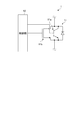
- FIG. 1 is a configuration diagram of a switching device 1 according to the first embodiment.
- FIG. 2 is a diagram for explaining a change in current by switching control of the switching device 1 according to the first embodiment.
- the switching device 1 includes a switching circuit unit 11 configured by switching elements and a control unit 12 that controls the switching elements.
- the switching circuit unit 11 includes an IGBT (Insulated Gate Bipolar Transistor) 11a as a first switching element that performs switching, and a MOSFET (Metal-Oxide-Semiconductor Field-Effect Transistor) 11b as a second switching element that performs switching. Connected to and configured.
- the MOSFET 11b is a switching element that has a higher switching speed than the IGBT 11a.
- the control unit 12 When performing the on control, the control unit 12 performs the turn-on of the IGBT 11a after the MOSFET 11b is turned on. When performing the off control, the control unit 12 performs the turn-off of the MOSFET 11b after performing the turn-off of the IGBT 11a.
- the turn-on means that the switching element is shifted from the off state to the on state.
- the turn-off refers to shifting the switching element from the on state to the off state.
- the IGBT 11a has a lower VCEsat than the MOSFET 11b. Further, the MOSFET 11b has a switching loss smaller than that of the IGBT 11a.
- FIG. 2 shows a change in the current flowing through the IGBT 11a due to turn-on and turn-off.
- B in FIG. 2 shows a change in VCE of the switching circuit unit 11 by turn-on and turn-off.
- C) in FIG. 2 shows a change in the current flowing through the MOSFET 11b due to turn-on and turn-off.
- D in FIG. 2 shows a change in the current flowing through the switching circuit unit 11 due to turn-on and turn-off.
- time t1 in FIG. 2 indicates the time until the set time elapses after the current flowing through the MOSFET 11b rises to the set value v1 based on the turn-on by the control unit 12.
- a time t2 in FIG. 2 indicates a time until the current flowing through the IGBT 11a rises to a set value v2 based on the turn-on by the control unit 12.
- the time required for the switching circuit unit 11 to turn on is the total time of the time t1 and the time t2.
- the time t3 in FIG. 2 indicates the time until the set time elapses after the current flowing through the IGBT 11a drops to the set value v3 based on the off control by the control unit 12.
- a time t4 in FIG. 2 indicates a time until the current flowing through the MOSFET 11b drops to the set value v4 based on the off control by the control unit 12.
- the time required for the switching circuit unit 11 to turn off is the total time of time t3 and time t4.
- the control unit 12 turns on the MOSFET 11b.
- the control unit 12 turns on the IGBT 11a at the timing when the time t1 has passed since the MOSFET 11b is turned on and a steady current starts to flow through the MOSFET 11b.
- the switching device 1 turns on the IGBT 11a, the current flows through the MOSFET 11b that is turned on first, and therefore the current is already flowing through the entire switching circuit 11.
- the resistance component of the IGBT 11 a is large from when the IGBT 11 a starts to turn on until it reaches a steady state, most of the current flows through the MOSFET 11 b.
- the VCEsat of the IGBT 11a is low in the switching device 1 when the IGBT 11a is in a steady state, the same current as that of the MOSFET 11b flows through the IGBT 11a.
- the switching device 1 as shown in FIGS. 2A and 2C, when the IGBT 11a is in a steady state, a steady current flows through the IGBT 11a, while a steady current flowing through the MOSFET 11b decreases.
- the control unit 12 turns off the IGBT 11a. Due to the turn-off, the resistance component of the IGBT 11a is increased. However, since the MOSFET 11b is in a steady state, the resistance component is low. Therefore, most of the current flows through the MOSFET 11b as shown in FIG.
- control unit 12 turns off the MOSFET 11b after the IGBT 11a is turned off.
- the MOSFET 11b having a smaller switching loss than the IGBT 11a is turned on first, so that the switching loss can be reduced.
- the switching device 1 can reduce the current flowing through the IGBT 11a that is turned on after the MOSFET 11b, the switching loss due to the IGBT 11a can be reduced.
- the switching device 1 since the switching device 1 has a low VCEsat of the IGBT 11a and the MOSFET 11b, the steady loss in the steady state can be reduced.
- the MOSFET 11b is turned off after the IGBT 11a is turned off, so that almost no current flows through the IGBT 11a, and the switching loss of the IGBT 11a can be reduced.
- the switching device 1 can reduce the switching loss when performing the off control.
- the switching device 1 does not cause a large current to flow through the IGBT 11a and the MOSFET 11b by performing the switching control as described above on the IGBT 11a and the MOSFET 11b, the switching circuit 11 is a large switching element in order to cope with the large current. Can be reduced in size.
- the switching device 1 since the switching device 1 has a fast on-control and off-control in the entire switching circuit unit 11 and uses a IGBT 11a and a MOSFET 11b in a steady state to flow a steady current at a low VCEsat, the switching loss and the steady loss are reduced. Thus, the load can be efficiently driven from a region where the operation load is small to a region where the operation load is large. In addition, since the switching device 1 can efficiently drive the load in the region where the operation load is large from the region where the operation load is small, the energy consumption can be reduced as compared with the conventional configuration, This has the effect of extending the life cycle and reducing the environmental impact.
- the second switching element has been described as a MOSFET, it may be an element formed of a wide band gap semiconductor made of SiC, GaN, or diamond, or a SJMOS (Super Junction Metal-Oxide-Semiconductor).
- a MOSFET Metal-Oxide-Semiconductor
- Embodiment 2 FIG. In the first embodiment, the configuration and operation of a switching device including a switching circuit in which two switching elements are connected in parallel have been described. In the second embodiment, the configuration and operation of a motor drive device 2 including a switching device will be described. .
- FIG. 3 is a configuration diagram of the motor drive device 2 according to the second embodiment.
- the motor drive device 2 includes a switching circuit unit 21 configured by switching elements, a motor unit 22 that converts electrical energy into mechanical energy, and a control unit 23 that controls the switching elements.
- IGBTs 21a, 22a, 23a, 24a, 25a, and 26a as first switching elements and MOSFETs 21b, 22b, 23b, 24b, 25b, and 26b as second switching elements are connected in parallel.
- One switching element group is configured, and a plurality of switching element groups are connected.
- the motor unit 22 is driven by the switching circuit unit 21.
- the motor unit 22 is exemplified by a three-phase motor.
- control unit 23 selects one or a plurality of switching element groups from the switching circuit unit 21 and performs on-control, the control unit 23 performs the first switching after turning on the second switching elements constituting the selected switching element group.
- the control unit 23 performs the first switching after turning on the second switching elements constituting the selected switching element group.
- the element is turned on and turned off, the first switching element constituting the selected switching element group is turned off and then the second switching element is turned off.
- the IGBTs 21a, 22a, 23a, 24a, 25a, and 26a are composed of switching elements having a low VCEsat and a slower switching speed than the MOSFETs 21b, 22b, 23b, 24b, 25b, and 26b.
- the MOSFETs 21b, 22b, 23b, 24b, 25b, and 26b are composed of switching elements having a low VCEsat and a faster switching speed than the IGBTs 21a, 22a, 23a, 24a, 25a, and 26a.
- the IGBT 21a and the MOSFET 21b, the IGBT 22a and the MOSFET 22b, the IGBT 23a and the MOSFET 23b are connected in parallel.
- the collector terminals of the IGBTs 21a, 22a, and 23a and the drain terminals of the MOSFETs 21b, 22b, and 23b are connected to the positive side of a DC power supply (not shown), the emitter terminals of the IGBTs 21a, 22a, and 23a, and the sources of the MOSFETs 21b, 22b, and 23b.
- the terminal is connected to the motor 22.
- the IGBT 24a and the MOSFET 24b, the IGBT 25a and the MOSFET 25b, the IGBT 26a and the MOSFET 26b are connected in parallel.
- the collector terminals of the IGBTs 24a, 25a and 26a and the drain terminals of the MOSFETs 24b, 25b and 26b are connected to the motor 22, and the emitter terminals of the IGBTs 24a, 25a and 26a and the source terminals of the MOSFETs 24b, 25b and 26b are not shown. Connected to the negative side of the DC power supply.
- the motor drive device 2 follows the on control and the off control described with reference to FIG. 2 in the first embodiment, and the IGBTs 21 a, 22 a, 23 a, 24 a, 25 a, 26 a and the MOSFETs 21 b, 22 b, Since switching control of 23b, 24b, 25b, and 26b is performed, it is not necessary to pass a large current through the IGBTs 21a, 22a, 23a, 24a, 25a, and 26a and the MOSFETs 21b, 22b, 23b, 24b, 25b, and 26b. In order to cope with the current, it is not necessary to configure the switching circuit 21 with a large switching element, and the size can be reduced.
- the motor drive device 2 has a fast on-control and off-control in the entire switching circuit unit 21, and in a steady state, the IGBTs 21a, 22a, 23a, 24a, 25a, 26a and the MOSFETs 21b, 22b, 23b, 24b, 25b, Since the steady current is caused to flow at a low VCEsat by using 26b, the switching loss and the steady loss can be reduced, and the motor 22 can be efficiently driven in the region where the operation load is large from the region where the operation load is small. Further, since the motor drive device 2 can efficiently drive the motor 22 in a region where the operation load is large from a region where the operation load is large, energy consumption can be reduced as compared with the conventional configuration. This also has the effect of extending the product life cycle and reducing the environmental impact.
- the load state or the temperature state is detected, and the drive control of the motor is performed based on the detection result.
- the motor drive device 2 since the switching operation can be performed in the same switching operation from the small current region where the load is small to the large current region where the load is large, it is not necessary to detect the load state or the temperature state. By performing on control and off control, switching loss and steady loss can be reduced.
- Embodiment 3 In the first embodiment, the configuration and operation of a switching device including a switching circuit in which two switching elements are connected in parallel have been described. In the third embodiment, the configuration and operation of a power conversion device 3 including a switching device will be described. .
- FIG. 4 is a configuration diagram of the power conversion device 3 according to the third embodiment.
- the power conversion device 3 is boosted by a rectifier circuit unit 31 that rectifies alternating current output from the alternating current power supply unit 4 into direct current, a booster circuit unit 32 that boosts the voltage, and a control unit 33 that controls the booster circuit unit 32. And a smoothing circuit unit 34 for smoothing the voltage.
- the power conversion device 3 converts AC power output from the AC power supply unit 4 into DC power, and supplies the converted DC power to the DC load 5.
- the rectifier circuit unit 32 is disposed in front of the switching circuit unit 31.
- the smoothing circuit unit 34 is disposed at the subsequent stage of the switching circuit unit 31.
- the step-up circuit unit 32 converts electrical energy into magnetic energy and stores it, and discharges the stored magnetic energy, a diode 42 that prevents backflow of current, and a switching circuit unit 43 that includes switching elements. With.
- the reactor 41 is connected to the plus side of the rectifier circuit unit 31.
- the diode 42 is connected to the output side of the reactor 41.
- a smoothing circuit unit 34 is connected to the cathode side of the diode 42.
- the switching circuit unit 43 is connected between a connection point between the output side of the reactor 42 and the anode side of the diode 42 and the minus side of the rectifying circuit unit 31.
- the switching circuit unit 43 has the same configuration as the switching circuit unit 11 described in the first embodiment, and an IGBT 43a as a first switching element that performs switching and a MOSFET 43b as a second switching element that performs switching are in parallel. It is connected.
- the IGBT 43a is composed of switching elements having a low VCEsat and a slower switching speed than the MOSFET 43b.
- the MOSFET 43b is composed of an element having a low VCEsat and a faster switching speed than the IGBT 43a.
- the control unit 33 controls the voltage across the smoothing circuit unit 34 to be a set DC voltage, and the current output from the AC power supply unit 4 is a sine in phase with the voltage output from the AC power supply unit 4. Power factor correction control is performed by controlling the switching circuit unit 43 so as to be a wave.
- control unit 33 performs switching control of the IGBT 43a and the MOSFET 43b in accordance with the on control and the off control described with reference to FIG. Do.
- the power conversion device 3 does not require a large current to flow through the IGBT 43a and the MOSFET 43b in the power factor correction control, it is not necessary to configure the switching circuit unit 43 with a large switching element to cope with the large current, and the power conversion device 3 can be downsized. can do.
- the power conversion device 3 has a fast ON control and an OFF control in the entire switching circuit unit 43 and allows a steady current to flow at a low VCEsat by using the IGBT 43a and the MOSFET 43b in a steady state, the switching loss and the steady loss are reduced.
- the DC load 5 can be efficiently driven in a region where the operation load is large from a region where the operation load is large.
- the power converter 3 can drive the DC load 5 efficiently in a region where the operation load is large from a region where the operation load is large, energy consumption can be reduced as compared with the conventional configuration. It can also increase the product life cycle and, as a result, reduce the environmental impact.
- the state or temperature state of the DC load 5 is detected, and power factor improvement control is performed based on the detection result.
- the switching operation can be performed in the same switching operation from the small current region where the load is small to the large current region where the load is large, it is not necessary to detect the state of the DC load 5 or the temperature state.
- the configuration described in the above embodiment shows an example of the contents of the present invention, and can be combined with another known technique, and can be combined with other configurations without departing from the gist of the present invention. It is also possible to omit or change the part.
Abstract
IGBT11aと、IGBT11aよりもスイッチング速度が速いMOSFET11bとが並列に接続されて構成されるスイッチング回路部11と、オン制御を行う場合、MOSFET11bのターンオンを行った後にIGBT11aのターンオンを行い、オフ制御を行う場合、IGBT11aのターンオフを行った後にMOSFET11bのターンオフを行う制御部12とを備えるスイッチング装置1を提供する。これにより、低負荷から高負荷の運転範囲において負荷を効率的に駆動することが可能になる。
Description
本発明は、スイッチング回路部の制御を行うスイッチング装置、モータ駆動装置、電力変換装置およびスイッチング方法に関する。
電力変換装置では、MOSFET(Metal-Oxide-Semiconductor Field-Effect Transistor)のようなスイッチングスピードが速いスイッチング素子を用いることによりスイッチングの際のスイッチング損失を低減させている。
また、スイッチングスピードの速いスイッチング素子と、スイッチングスピードが遅いが定常損失の低いスイッチング素子とを並列に接続し、負荷の大きさに基づいてスイッチング素子を切り替える装置が提案されている(下記特許文献1)。なお、特許文献1では、スイッチングスピードの速いスイッチング素子は、MOSFETが例示され、スイッチングスピードが遅いが定常損失の低いスイッチング素子は、IGBT(Insulated Gate Bipolar Transistor)が例示されている。
特許文献1には、「電流I1より小さいときは従来どおりFETで損失を小さくし、電流I1より大きいときはIGBTに負担を大きくさせFETの損失増加を小さく」することが記載されている。
ところで、電力変換装置に用いられているIGBTは、コレクタエミッタ間飽和電圧が大きいと、定常状態におけるコレクタエミッタ間飽和電圧による損失が大きくなってしまう。そのため、定常状態における損失を低減させるのに、コレクタエミッタ間飽和電圧が低いスイッチング素子が必要とされている。以下では、コレクタエミッタ間飽和電圧は、VCEsatと称する。
近年、スイッチングスピードが速く、VCEsatの低いスイッチング素子が開発されているが、大電流に対応させようとすると、スイッチング素子のサイズを大きくする必要があり、価格が高くなってしまう。
また、従来から、低コストでVCEsatが低く大電流を流せるスイッチング素子は存在するが、高耐圧のスイッチング素子の場合、VCEsatが低いと、スイッチングスピードが遅く、ターンオンまたはターンオフの際のスイッチング損失が大きいという問題がある。
上述した特許文献1は、運転負荷が小さくスイッチングの多い領域において、スイッチングスピードの速いMOSFETを使用するので、スイッチングにおけるスイッチング損失を低減することができるが、定常状態における定常損失が増大し、一方、運転負荷が大きくスイッチングが少ない領域において、スイッチングスピードの遅いIGBTを利用するので、定常状態における定常損失を低減することができるが、スイッチング時におけるスイッチング損失が増大する問題があり、運転負荷が小さい領域から運転負荷が大きい領域において負荷を効率的に駆動することができない。
本発明は、上記に鑑みてなされたものであり、運転負荷が小さい領域から運転負荷が大きい領域において負荷を効率的に駆動することができるスイッチング装置、モータ駆動装置、電力変換装置およびスイッチング方法を提供することを目的とする。
上述した課題を解決し、目的を達成するために、本発明に係るスイッチング装置は、第1スイッチング素子と、前記第1スイッチング素子よりもスイッチング速度が速い第2スイッチング素子とが並列に接続されて構成されるスイッチング回路部と、オン制御を行う場合、前記第2スイッチング素子のターンオンを行った後に前記第1スイッチング素子のターンオンを行い、オフ制御を行う場合、前記第1スイッチング素子のターンオフを行った後に前記第2スイッチング素子のターンオフを行う制御部とを備える。
本発明によれば、運転負荷が小さい領域から運転負荷が大きい領域において負荷を効率的に駆動することができる。
以下に、本発明の実施の形態に係るスイッチング装置、モータ駆動装置、電力変換装置およびスイッチング方法を図面に基づいて詳細に説明する。なお、この実施の形態によりこの発明が限定されるものではない。
実施の形態1.
図1は、実施の形態1に係るスイッチング装置1の構成図である。図2は、実施の形態1に係るスイッチング装置1のスイッチング制御による電流の変化についての説明に供する図である。
図1は、実施の形態1に係るスイッチング装置1の構成図である。図2は、実施の形態1に係るスイッチング装置1のスイッチング制御による電流の変化についての説明に供する図である。
スイッチング装置1は、スイッチング素子により構成されているスイッチング回路部11と、スイッチング素子を制御する制御部12とを備える。
スイッチング回路部11は、スイッチングを行う第1スイッチング素子としてのIGBT(Insulated Gate Bipolar Transistor)11aと、スイッチングを行う第2スイッチング素子としてのMOSFET(Metal-Oxide-Semiconductor Field-Effect Transistor)11bとが並列に接続されて構成されている。また、MOSFET11bは、IGBT11aよりも、スイッチング速度が速いスイッチング素子である。
制御部12は、オン制御を行う場合、MOSFET11bのターンオンを行った後にIGBT11aのターンオンを行い、オフ制御を行う場合、IGBT11aのターンオフを行った後にMOSFET11bのターンオフを行う。ターンオンとは、スイッチング素子をオフ状態からオン状態に移行させることをいう。ターンオフとは、スイッチング素子をオン状態からオフ状態に移行することをいう。
IGBT11aは、MOSFET11bよりもVCEsatが低い。また、MOSFET11bは、IGBT11aよりもスイッチング損失が小さい。
ここで、スイッチング装置1の具体的な動作について図2を参照しながら説明する。なお、図2中の(a)は、ターンオンおよびターンオフによりIGBT11aに流れる電流の変化を示している。図2中の(b)は、ターンオンおよびターンオフによりスイッチング回路部11のVCEの変化を示している。図2中の(c)は、ターンオンおよびターンオフによりMOSFET11bに流れる電流の変化を示している。図2中の(d)は、ターンオンおよびターンオフによりスイッチング回路部11に流れる電流の変化を示している。
また、図2中の時間t1は、制御部12によるターンオンに基づいて、MOSFET11bに流れる電流が設定された値v1まで上昇した後、設定された時間が経過するまでの時間を示している。図2中の時間t2は、制御部12によるターンオンに基づいて、IGBT11aに流れる電流が設定された値v2まで上昇するまでの時間を示している。スイッチング回路部11がターンオンに要する時間は、時間t1と時間t2の合計時間である。
図2中の時間t3は、制御部12によるオフ制御に基づいて、IGBT11aに流れる電流が設定された値v3まで下降した後、設定された時間が経過するまでの時間を示している。図2中の時間t4は、制御部12によるオフ制御に基づいて、MOSFET11bに流れる電流が設定された値v4まで下降するまでの時間を示している。スイッチング回路部11がターンオフに要する時間は、時間t3と時間t4の合計時間である。
まず、オン制御について説明する。制御部12は、MOSFET11bをターンオンする。制御部12は、MOSFET11bをターンオンしてから時間t1が経過し、MOSFET11bに定常電流が流れ始めたタイミングでIGBT11aをターンオンする。
上述したように、スイッチング装置1は、IGBT11aをターンオンするときには、先にターンオンしているMOSFET11bに電流が流れているため、スイッチング回路11全体ではすでに電流が流れている。
また、スイッチング装置1は、IGBT11aがターンオンし始めてから定常状態になるまでの間は、IGBT11aの抵抗成分が大きいため、殆どの電流はMOSFET11bに流れる。
また、スイッチング装置1は、IGBT11aが定常状態になると、IGBT11aのVCEsatが低いため、MOSFET11bと同じ電流がIGBT11aに流れる。スイッチング装置1は、図2(a)、(c)に示すように、IGBT11aが定常状態になると、IGBT11aにも定常電流が流れる一方、MOSFET11bに流れていた定常電流が小さくなる。
次に、オフ制御を行う場合について説明する。制御部12は、IGBT11aをターンオフする。ターンオフにより、IGBT11aの抵抗成分は、高くなる。しかし、MOSFET11bは、定常状態にあるので抵抗成分が低い。よって、殆どの電流は、図2(c)に示すように、MOSFET11bに流れる。
そして、制御部12は、IGBT11aがオフになった後にMOSFET11bをターンオフする。
よって、スイッチング装置1は、オン制御を行う場合、IGBT11aよりもスイッチング損失が小さいMOSFET11bを先にターンオンするため、スイッチング損失を小さくすることができる。
また、スイッチング装置1は、MOSFET11bの後にターンオンするIGBT11aに流れる電流を小さくできるので、IGBT11aによるスイッチング損失を小さくすることができる。
また、スイッチング装置1は、IGBT11aおよびMOSFET11bのVCEsatが低いため、定常状態における定常損失も小さくすることができる。
また、スイッチング装置1は、オフ制御を行う場合、IGBT11aをターンオフした後に、MOSFET11bをターンオフするので、IGBT11aに電流が殆ど流れず、IGBT11aのスイッチング損失を小さくすることができる。
また、スイッチング装置1は、IGBT11aの後にターンオフするMOSFET11bのスイッチング損失が小さいので、オフ制御を行うときのスイッチング損失を小さくすることができる。
また、スイッチング装置1は、IGBT11aおよびMOSFET11bを上述のようなスイッチング制御を行うことにより、IGBT11aおよびMOSFET11bに大電流を流さなくてすむので、大電流に対応するために大型のスイッチング素子でスイッチング回路11を構成する必要がなく、小型化することができる。
さらに、スイッチング装置1は、スイッチング回路部11全体で、オン制御およびオフ制御が速く、かつ、定常状態においてIGBT11aおよびMOSFET11bを用いることによって低いVCEsatで定常電流を流すので、スイッチング損失および定常損失を低減することができ、運転負荷が小さい領域から運転負荷が大きい領域において負荷を効率的に駆動することができる。また、スイッチング装置1は、運転負荷が小さい領域から運転負荷が大きい領域において負荷を効率的に駆動することができるので、従来の構成に比して、エネルギー消費量を削減することができ、製品のライフサイクルを伸ばし、結果、環境負荷を低減する効果もある。
なお、第2スイッチング素子は、MOSFETとして説明したが、SiC、GaN、またはダイヤモンドを材料とするワイドバンドギャップ半導体で形成された素子、またはSJMOS(Super Junction Metal-Oxide-Semiconductor)でもよい。
実施の形態2.
実施の形態1では二つのスイッチング素子を並列に接続したスイッチング回路を備えるスイッチング装置の構成と動作について説明したが、実施の形態2では、スイッチング装置を備えるモータ駆動装置2の構成と動作について説明する。
実施の形態1では二つのスイッチング素子を並列に接続したスイッチング回路を備えるスイッチング装置の構成と動作について説明したが、実施の形態2では、スイッチング装置を備えるモータ駆動装置2の構成と動作について説明する。
図3は、実施の形態2に係るモータ駆動装置2の構成図である。モータ駆動装置2は、スイッチング素子により構成されているスイッチング回路部21と、電気エネルギーを機械エネルギーに変換するモータ部22と、スイッチング素子を制御する制御部23とを備える。
スイッチング回路部21は、第1スイッチング素子としてのIGBT21a、22a、23a、24a、25a、26aと第2スイッチング素子としてのMOSFET21b、22b、23b、24b、25b、26bとが並列に接続されることにより一のスイッチング素子群を構成し、スイッチング素子群が複数個接続されることにより構成される。
モータ部22は、スイッチング回路部21により駆動される。モータ部22は、三相電動機が例示される。
制御部23は、スイッチング回路部21の中から一又は複数のスイッチング素子群を選択し、オン制御を行う場合、選択したスイッチング素子群を構成する第2スイッチング素子のターンオンを行った後に第1スイッチング素子のターンオンを行い、オフ制御を行う場合、選択したスイッチング素子群を構成する第1スイッチング素子のターンオフを行った後に第2スイッチング素子のターンオフを行う。
ここで、モータ駆動装置2の詳細な構成について説明する。
IGBT21a、22a、23a、24a、25a、26aは、VCEsatが低く、MOSFET21b、22b、23b、24b、25b、26bよりもスイッチングスピードが遅いスイッチング素子で構成されている。
MOSFET21b、22b、23b、24b、25b、26bは、VCEsatが低く、IGBT21a、22a、23a、24a、25a、26aよりもスイッチングスピードが速いスイッチング素子で構成されている。
また、IGBT21aおよびMOSFET21b、IGBT22aおよびMOSFET22b、IGBT23aおよびMOSFET23bは、並列に接続されている。
IGBT21a、22a、23aのコレクタ端子と、MOSFET21b、22b、23bのドレイン端子とは、不図示の直流電源のプラス側に接続され、IGBT21a、22a、23aのエミッタ端子と、MOSFET21b、22b、23bのソース端子は、モータ22に接続される。
また、IGBT24aおよびMOSFET24b、IGBT25aおよびMOSFET25b、IGBT26aおよびMOSFET26bは、並列に接続されている。
IGBT24a、25a、26aのコレクタ端子と、MOSFET24b、25b、26bのドレイン端子とは、モータ22に接続され、IGBT24a、25a、26aのエミッタ端子と、MOSFET24b、25b、26bのソース端子は、不図示の直流電源のマイナス側に接続されている。
モータ駆動装置2は、モータ22を駆動するために、実施の形態1において図2を用いて説明したオン制御およびオフ制御にしたがって、IGBT21a、22a、23a、24a、25a、26aとMOSFET21b、22b、23b、24b、25b、26bのスイッチングとをスイッチング制御するので、IGBT21a、22a、23a、24a、25a、26aおよびMOSFET21b、22b、23b、24b、25b、26bに大電流を流さなくてすむので、大電流に対応するために大型のスイッチング素子でスイッチング回路21を構成する必要がなく、小型化することができる。
さらに、モータ駆動装置2は、スイッチング回路部21全体で、オン制御およびオフ制御が速く、かつ、定常状態においてIGBT21a、22a、23a、24a、25a、26aおよびMOSFET21b、22b、23b、24b、25b、26bを用いることによって低いVCEsatで定常電流を流すので、スイッチング損失および定常損失を低減することができ、運転負荷が小さい領域から運転負荷が大きい領域においてモータ22を効率的に駆動することができる。また、モータ駆動装置2は、運転負荷が小さい領域から運転負荷が大きい領域においてモータ22を効率的に駆動することができるので、従来の構成に比して、エネルギー消費量を削減することができ、製品のライフサイクルを伸ばし、結果、環境負荷を低減する効果もある。
また、従来の装置では、負荷の状態または温度状態を検出し、検出結果に基づいてモータの駆動制御を行っていた。モータ駆動装置2では、スイッチング動作を負荷が小さい小電流の領域から負荷が大きい大電流の領域まで、同じスイッチング動作で行うことができるため、負荷の状態または温度状態の検出を不要とし、上述したオン制御およびオフ制御を行うことにより、スイッチング損失および定常損失を低減することができる。
実施の形態3.
実施の形態1では二つのスイッチング素子を並列に接続したスイッチング回路を備えるスイッチング装置の構成と動作について説明したが、実施の形態3では、スイッチング装置を備える電力変換装置3の構成と動作について説明する。
実施の形態1では二つのスイッチング素子を並列に接続したスイッチング回路を備えるスイッチング装置の構成と動作について説明したが、実施の形態3では、スイッチング装置を備える電力変換装置3の構成と動作について説明する。
図4は、実施の形態3に係る電力変換装置3の構成図である。電力変換装置3は、交流電源部4から出力された交流を直流に整流する整流回路部31と、電圧を昇圧する昇圧回路部32と、昇圧回路部32を制御する制御部33と、昇圧された電圧を平滑する平滑回路部34とを備える。電力変換装置3は、交流電源部4から出力された交流電力を直流電力に変換し、変換した直流電力を直流負荷5に供給する。
図4に示すように、整流回路部32は、スイッチング回路部31の前段に配置される。平滑回路部34は、スイッチング回路部31の後段に配置される。
昇圧回路部32は、電気エネルギーを磁気エネルギーに変換して蓄積し、蓄積した磁気エネルギーを放出するリアクタ41と、電流の逆流を防止するダイオード42と、スイッチング素子により構成されているスイッチング回路部43とを備える。
リアクタ41は、整流回路部31のプラス側に接続される。ダイオード42は、リアクタ41の出力側に接続される。ダイオード42のカソード側には、平滑回路部34が接続される。スイッチング回路部43は、リアクタ42の出力側とダイオード42のアノード側との接続点と、整流回路部31のマイナス側との間に接続される。
スイッチング回路部43は、実施の形態1で説明したスイッチング回路部11と同様の構成であり、スイッチングを行う第1スイッチング素子としてのIGBT43aと、スイッチングを行う第2スイッチング素子としてのMOSFET43bとが並列に接続されている。
IGBT43aは、VCEsatが低く、MOSFET43bよりもスイッチングスピードが遅いスイッチング素子で構成されている。
MOSFET43bは、VCEsatが低く、IGBT43aよりもスイッチングスピードが速い素子で構成されている。
制御部33は、平滑回路部34の両端電圧が、設定された直流電圧になるように制御し、交流電源部4から出力される電流が交流電源部4から出力される電圧と同位相の正弦波になるように、スイッチング回路部43を制御することにより、力率改善制御を行う。
制御部33は、直流負荷5を駆動するために、実施の形態1において図2を用いて説明したオン制御およびオフ制御にしたがって、IGBT43aとMOSFET43bとをスイッチング制御することにより、力率改善制御を行う。
電力変換装置3は、力率改善制御において、IGBT43aおよびMOSFET43bに大電流を流さなくてすむので、大電流に対応するために大型のスイッチング素子でスイッチング回路部43を構成する必要がなく、小型化することができる。
さらに、電力変換装置3は、スイッチング回路部43全体で、オン制御およびオフ制御が速く、かつ、定常状態においてIGBT43aおよびMOSFET43bを用いることによって低いVCEsatで定常電流を流すので、スイッチング損失および定常損失を低減することができ、運転負荷が小さい領域から運転負荷が大きい領域において直流負荷5を効率的に駆動することができる。また、電力変換装置3は、運転負荷が小さい領域から運転負荷が大きい領域において直流負荷5を効率的に駆動することができるので、従来の構成に比して、エネルギー消費量を削減することができ、製品のライフサイクルを伸ばし、結果、環境負荷を低減する効果もある。
また、従来の装置では、直流負荷5の状態または温度状態を検出し、検出結果に基づいて力率改善制御を行っていた。電力変換装置3では、スイッチング動作を負荷が小さい小電流の領域から負荷が大きい大電流の領域まで、同じスイッチング動作で行うことができるため、直流負荷5の状態または温度状態の検出を不要とし、上述したオン制御およびオフ制御を行うことにより、力率改善制御の際のスイッチング損失および定常損失を低減することができる。
以上の実施の形態に示した構成は、本発明の内容の一例を示すものであり、別の公知の技術と組み合わせることも可能であるし、本発明の要旨を逸脱しない範囲で、構成の一部を省略、変更することも可能である。
1 スイッチング装置、2 モータ駆動装置、3 電力変換装置、4 交流電源部、5 直流負荷、11,21,43 スイッチング回路部、12,23 制御部、11a,21a,22a,23a,24a,25a,26a,43a IGBT、11b,21b,22b,23b,24b,25b,26b,43b MOSFET、22 モータ部、31 整流回路部、32 昇圧回路部、33 制御部、34 平滑回路部。
Claims (5)
- 第1スイッチング素子と、前記第1スイッチング素子よりもスイッチング速度が速い第2スイッチング素子とが並列に接続されて構成されるスイッチング回路部と、
オン制御を行う場合、前記第2スイッチング素子のターンオンを行った後に前記第1スイッチング素子のターンオンを行い、オフ制御を行う場合、前記第1スイッチング素子のターンオフを行った後に前記第2スイッチング素子のターンオフを行う制御部とを備えるスイッチング装置。 - 前記第1スイッチング素子は、前記第2スイッチング素子よりもコレクタエミッタ間飽和電圧が低く、
前記第2スイッチング素子は、前記第1スイッチング素子よりもスイッチング損失が小さい請求項1記載のスイッチング装置。 - 請求項1記載のスイッチング装置を備えるモータ駆動装置であって、
前記第1スイッチング素子および前記第2スイッチング素子が並列に接続されることにより一のスイッチング素子群を構成し、前記スイッチング素子群が複数個接続されることにより構成されるスイッチング回路部と、
前記スイッチング回路部により駆動されるモータ部とを備え、
前記スイッチング装置の制御部は、前記スイッチング回路部の中から一又は複数のスイッチング素子群を選択し、オン制御を行う場合、選択したスイッチング素子群を構成する第2スイッチング素子のターンオンを行った後に第1スイッチング素子のターンオンを行い、オフ制御を行う場合、選択したスイッチング素子群を構成する第1スイッチング素子のターンオフを行った後に第2スイッチング素子のターンオフを行うモータ駆動装置。 - 請求項1記載のスイッチング装置を備える電力変換装置であって、
前記スイッチング装置のスイッチング回路部の前段に配置される整流回路部と、
前記スイッチング回路部の後段に配置される平滑回路部とを備える電力変換装置。 - 第1スイッチング素子と、前記第1スイッチング素子よりも、スイッチング速度が速い第2スイッチング素子とが並列に接続されて構成されるスイッチング回路部を備えるスイッチング装置のスイッチング方法において、
オン制御を行う場合、
前記第2スイッチング素子のターンオンを行う第1工程と、
前記第1工程の後に前記第1スイッチング素子のターンオンを行う第2工程と、
オフ制御を行う場合、
前記第1スイッチング素子のターンオフを行う第3工程と、
前記第3工程の後に前記第2スイッチング素子のターンオフを行う第4工程とを有するスイッチング方法。
Priority Applications (3)
| Application Number | Priority Date | Filing Date | Title |
|---|---|---|---|
| EP14900339.4A EP3240177A4 (en) | 2014-12-22 | 2014-12-22 | Switching device, motor drive device, power conversion device, and switching method |
| PCT/JP2014/083942 WO2016103328A1 (ja) | 2014-12-22 | 2014-12-22 | スイッチング装置、モータ駆動装置、電力変換装置およびスイッチング方法 |
| JP2016565627A JPWO2016103328A1 (ja) | 2014-12-22 | 2014-12-22 | スイッチング装置、モータ駆動装置、電力変換装置およびスイッチング方法 |
Applications Claiming Priority (1)
| Application Number | Priority Date | Filing Date | Title |
|---|---|---|---|
| PCT/JP2014/083942 WO2016103328A1 (ja) | 2014-12-22 | 2014-12-22 | スイッチング装置、モータ駆動装置、電力変換装置およびスイッチング方法 |
Publications (1)
| Publication Number | Publication Date |
|---|---|
| WO2016103328A1 true WO2016103328A1 (ja) | 2016-06-30 |
Family
ID=56149432
Family Applications (1)
| Application Number | Title | Priority Date | Filing Date |
|---|---|---|---|
| PCT/JP2014/083942 WO2016103328A1 (ja) | 2014-12-22 | 2014-12-22 | スイッチング装置、モータ駆動装置、電力変換装置およびスイッチング方法 |
Country Status (3)
| Country | Link |
|---|---|
| EP (1) | EP3240177A4 (ja) |
| JP (1) | JPWO2016103328A1 (ja) |
| WO (1) | WO2016103328A1 (ja) |
Cited By (3)
| Publication number | Priority date | Publication date | Assignee | Title |
|---|---|---|---|---|
| JP2019080371A (ja) * | 2017-10-20 | 2019-05-23 | 株式会社デンソー | スイッチの駆動回路 |
| JP2020061810A (ja) * | 2018-10-05 | 2020-04-16 | トヨタ自動車株式会社 | 制御装置 |
| WO2023079820A1 (ja) * | 2021-11-08 | 2023-05-11 | ローム株式会社 | 半導体装置 |
Families Citing this family (4)
| Publication number | Priority date | Publication date | Assignee | Title |
|---|---|---|---|---|
| DE102017105712A1 (de) | 2017-03-16 | 2018-10-04 | Infineon Technologies Austria Ag | Transistorbauelement |
| CN109698608A (zh) * | 2018-12-21 | 2019-04-30 | 江苏固德威电源科技股份有限公司 | 一种开关器件及其采用的控制方法 |
| DE102021203851A1 (de) | 2021-04-19 | 2022-10-20 | Zf Friedrichshafen Ag | Inverteraufbau eines Elektronikmoduls für einen Elektroantrieb eines Fahrzeugs |
| EP4207601A1 (en) * | 2021-12-28 | 2023-07-05 | Infineon Technologies Austria AG | Electronic circuit and buck converter including the electronic circuit |
Citations (3)
| Publication number | Priority date | Publication date | Assignee | Title |
|---|---|---|---|---|
| JPH08140355A (ja) * | 1994-09-12 | 1996-05-31 | Fuji Electric Co Ltd | スイッチング電源 |
| JPH1080152A (ja) | 1996-09-06 | 1998-03-24 | Hitachi Ltd | フォークリフト用インバータ装置 |
| JP2012249509A (ja) * | 2011-05-02 | 2012-12-13 | Mitsubishi Electric Corp | 電力用半導体装置 |
Family Cites Families (3)
| Publication number | Priority date | Publication date | Assignee | Title |
|---|---|---|---|---|
| JP2009142070A (ja) * | 2007-12-06 | 2009-06-25 | Fuji Electric Systems Co Ltd | 電力用半導体素子のゲート駆動方式 |
| JP5932269B2 (ja) * | 2011-09-08 | 2016-06-08 | 株式会社東芝 | パワー半導体モジュール及びパワー半導体モジュールの駆動方法 |
| JP5591213B2 (ja) * | 2011-11-25 | 2014-09-17 | 三菱電機株式会社 | インバータ装置、およびそれを備えた空気調和機 |
-
2014
- 2014-12-22 WO PCT/JP2014/083942 patent/WO2016103328A1/ja active Application Filing
- 2014-12-22 EP EP14900339.4A patent/EP3240177A4/en not_active Withdrawn
- 2014-12-22 JP JP2016565627A patent/JPWO2016103328A1/ja active Pending
Patent Citations (3)
| Publication number | Priority date | Publication date | Assignee | Title |
|---|---|---|---|---|
| JPH08140355A (ja) * | 1994-09-12 | 1996-05-31 | Fuji Electric Co Ltd | スイッチング電源 |
| JPH1080152A (ja) | 1996-09-06 | 1998-03-24 | Hitachi Ltd | フォークリフト用インバータ装置 |
| JP2012249509A (ja) * | 2011-05-02 | 2012-12-13 | Mitsubishi Electric Corp | 電力用半導体装置 |
Non-Patent Citations (1)
| Title |
|---|
| See also references of EP3240177A4 * |
Cited By (4)
| Publication number | Priority date | Publication date | Assignee | Title |
|---|---|---|---|---|
| JP2019080371A (ja) * | 2017-10-20 | 2019-05-23 | 株式会社デンソー | スイッチの駆動回路 |
| JP2020061810A (ja) * | 2018-10-05 | 2020-04-16 | トヨタ自動車株式会社 | 制御装置 |
| JP7180264B2 (ja) | 2018-10-05 | 2022-11-30 | 株式会社デンソー | 制御装置 |
| WO2023079820A1 (ja) * | 2021-11-08 | 2023-05-11 | ローム株式会社 | 半導体装置 |
Also Published As
| Publication number | Publication date |
|---|---|
| JPWO2016103328A1 (ja) | 2017-04-27 |
| EP3240177A4 (en) | 2018-01-03 |
| EP3240177A1 (en) | 2017-11-01 |
Similar Documents
| Publication | Publication Date | Title |
|---|---|---|
| WO2016103328A1 (ja) | スイッチング装置、モータ駆動装置、電力変換装置およびスイッチング方法 | |
| JP5521796B2 (ja) | 整流回路 | |
| WO2012176403A1 (ja) | 昇降圧型ac/dcコンバータ | |
| JP5940133B2 (ja) | 直流電源装置および電力変換方法 | |
| US8901906B2 (en) | Control circuit and electronic apparatus using the same | |
| JP5950890B2 (ja) | 電源装置、およびその電源装置を備えた空気調和機 | |
| JP2009011013A (ja) | 電力変換装置 | |
| JP2017195691A (ja) | 電力変換装置 | |
| JP2010172078A (ja) | スイッチ回路 | |
| US9479049B2 (en) | Semiconductor module and boost rectifier circuit | |
| JP2017028878A (ja) | 電力変換装置 | |
| US20150207428A1 (en) | Inverter drive circuit | |
| US10938318B2 (en) | AC-DC converting apparatus, motor drive control apparatus, blower, compressor, and air conditioner | |
| JP2007129848A (ja) | インバータ装置 | |
| JP2010124627A (ja) | ゲート回路 | |
| JP2006158001A (ja) | インバータ装置 | |
| JP6705234B2 (ja) | インバータ装置の制御方法 | |
| JP2015204723A (ja) | 半導体装置及びそれを用いた電力変換装置 | |
| RU98651U1 (ru) | Ключевой усилитель мощности | |
| JP5734120B2 (ja) | 電力変換装置 | |
| JP7063082B2 (ja) | スイッチング素子制御回路 | |
| JP5857189B2 (ja) | インバータ装置 | |
| JP2018082525A (ja) | スイッチング装置 | |
| JP2018121475A (ja) | 電力変換装置 | |
| CN111615783B (zh) | 半导体元件的驱动电路、半导体元件的驱动方法以及马达控制装置 |
Legal Events
| Date | Code | Title | Description |
|---|---|---|---|
| REEP | Request for entry into the european phase |
Ref document number: 2014900339 Country of ref document: EP |
|
| 121 | Ep: the epo has been informed by wipo that ep was designated in this application |
Ref document number: 14900339 Country of ref document: EP Kind code of ref document: A1 |
|
| ENP | Entry into the national phase |
Ref document number: 2016565627 Country of ref document: JP Kind code of ref document: A |
|
| NENP | Non-entry into the national phase |
Ref country code: DE |