WO2016098518A1 - SUBSTRAT EN GaN - Google Patents
SUBSTRAT EN GaN Download PDFInfo
- Publication number
- WO2016098518A1 WO2016098518A1 PCT/JP2015/082439 JP2015082439W WO2016098518A1 WO 2016098518 A1 WO2016098518 A1 WO 2016098518A1 JP 2015082439 W JP2015082439 W JP 2015082439W WO 2016098518 A1 WO2016098518 A1 WO 2016098518A1
- Authority
- WO
- WIPO (PCT)
- Prior art keywords
- gan
- substrate
- gan substrate
- crystal
- plane
- Prior art date
Links
- JMASRVWKEDWRBT-UHFFFAOYSA-N Gallium nitride Chemical compound [Ga]#N JMASRVWKEDWRBT-UHFFFAOYSA-N 0.000 title claims abstract description 295
- 238000002441 X-ray diffraction Methods 0.000 claims abstract description 39
- 239000013078 crystal Substances 0.000 claims description 226
- 239000000758 substrate Substances 0.000 claims description 100
- 229910052783 alkali metal Inorganic materials 0.000 claims description 7
- 150000001340 alkali metals Chemical class 0.000 claims description 7
- 229910052736 halogen Inorganic materials 0.000 claims description 5
- 150000002367 halogens Chemical class 0.000 claims description 5
- 238000010521 absorption reaction Methods 0.000 claims description 4
- GYHNNYVSQQEPJS-UHFFFAOYSA-N Gallium Chemical compound [Ga] GYHNNYVSQQEPJS-UHFFFAOYSA-N 0.000 claims description 3
- 238000000862 absorption spectrum Methods 0.000 claims description 3
- 229910052733 gallium Inorganic materials 0.000 claims description 3
- 239000001257 hydrogen Substances 0.000 claims description 3
- 229910052739 hydrogen Inorganic materials 0.000 claims description 3
- 229910002601 GaN Inorganic materials 0.000 description 140
- 238000000034 method Methods 0.000 description 59
- 238000002248 hydride vapour-phase epitaxy Methods 0.000 description 24
- 239000004065 semiconductor Substances 0.000 description 16
- IJGRMHOSHXDMSA-UHFFFAOYSA-N Atomic nitrogen Chemical compound N#N IJGRMHOSHXDMSA-UHFFFAOYSA-N 0.000 description 11
- 238000000227 grinding Methods 0.000 description 10
- 238000004519 manufacturing process Methods 0.000 description 10
- 238000012360 testing method Methods 0.000 description 10
- 150000004767 nitrides Chemical class 0.000 description 9
- 238000002474 experimental method Methods 0.000 description 8
- QGZKDVFQNNGYKY-UHFFFAOYSA-N Ammonia Chemical compound N QGZKDVFQNNGYKY-UHFFFAOYSA-N 0.000 description 6
- 238000012545 processing Methods 0.000 description 6
- 238000005259 measurement Methods 0.000 description 5
- 239000002994 raw material Substances 0.000 description 5
- 239000012535 impurity Substances 0.000 description 4
- 229910052757 nitrogen Inorganic materials 0.000 description 4
- ZCYVEMRRCGMTRW-UHFFFAOYSA-N 7553-56-2 Chemical group [I] ZCYVEMRRCGMTRW-UHFFFAOYSA-N 0.000 description 3
- 229910017855 NH 4 F Inorganic materials 0.000 description 3
- 229910021529 ammonia Inorganic materials 0.000 description 3
- 239000012159 carrier gas Substances 0.000 description 3
- 150000001875 compounds Chemical class 0.000 description 3
- 238000005520 cutting process Methods 0.000 description 3
- 229910001873 dinitrogen Inorganic materials 0.000 description 3
- 238000004090 dissolution Methods 0.000 description 3
- 125000001153 fluoro group Chemical group F* 0.000 description 3
- UPWPDUACHOATKO-UHFFFAOYSA-K gallium trichloride Chemical compound Cl[Ga](Cl)Cl UPWPDUACHOATKO-UHFFFAOYSA-K 0.000 description 3
- XMBWDFGMSWQBCA-UHFFFAOYSA-N hydrogen iodide Chemical compound I XMBWDFGMSWQBCA-UHFFFAOYSA-N 0.000 description 3
- 239000000463 material Substances 0.000 description 3
- 238000002488 metal-organic chemical vapour deposition Methods 0.000 description 3
- 239000012808 vapor phase Substances 0.000 description 3
- 238000012795 verification Methods 0.000 description 3
- 238000005530 etching Methods 0.000 description 2
- 238000007716 flux method Methods 0.000 description 2
- 229910000043 hydrogen iodide Inorganic materials 0.000 description 2
- 239000011777 magnesium Substances 0.000 description 2
- 238000002360 preparation method Methods 0.000 description 2
- 238000001004 secondary ion mass spectrometry Methods 0.000 description 2
- 239000011734 sodium Substances 0.000 description 2
- 238000010897 surface acoustic wave method Methods 0.000 description 2
- DDFHBQSCUXNBSA-UHFFFAOYSA-N 5-(5-carboxythiophen-2-yl)thiophene-2-carboxylic acid Chemical compound S1C(C(=O)O)=CC=C1C1=CC=C(C(O)=O)S1 DDFHBQSCUXNBSA-UHFFFAOYSA-N 0.000 description 1
- 229910002704 AlGaN Inorganic materials 0.000 description 1
- ZAMOUSCENKQFHK-UHFFFAOYSA-N Chlorine atom Chemical compound [Cl] ZAMOUSCENKQFHK-UHFFFAOYSA-N 0.000 description 1
- PXGOKWXKJXAPGV-UHFFFAOYSA-N Fluorine Chemical compound FF PXGOKWXKJXAPGV-UHFFFAOYSA-N 0.000 description 1
- DGAQECJNVWCQMB-PUAWFVPOSA-M Ilexoside XXIX Chemical compound C[C@@H]1CC[C@@]2(CC[C@@]3(C(=CC[C@H]4[C@]3(CC[C@@H]5[C@@]4(CC[C@@H](C5(C)C)OS(=O)(=O)[O-])C)C)[C@@H]2[C@]1(C)O)C)C(=O)O[C@H]6[C@@H]([C@H]([C@@H]([C@H](O6)CO)O)O)O.[Na+] DGAQECJNVWCQMB-PUAWFVPOSA-M 0.000 description 1
- XEEYBQQBJWHFJM-UHFFFAOYSA-N Iron Chemical compound [Fe] XEEYBQQBJWHFJM-UHFFFAOYSA-N 0.000 description 1
- WHXSMMKQMYFTQS-UHFFFAOYSA-N Lithium Chemical compound [Li] WHXSMMKQMYFTQS-UHFFFAOYSA-N 0.000 description 1
- FYYHWMGAXLPEAU-UHFFFAOYSA-N Magnesium Chemical compound [Mg] FYYHWMGAXLPEAU-UHFFFAOYSA-N 0.000 description 1
- ZLMJMSJWJFRBEC-UHFFFAOYSA-N Potassium Chemical compound [K] ZLMJMSJWJFRBEC-UHFFFAOYSA-N 0.000 description 1
- XUIMIQQOPSSXEZ-UHFFFAOYSA-N Silicon Chemical compound [Si] XUIMIQQOPSSXEZ-UHFFFAOYSA-N 0.000 description 1
- 238000004854 X-ray topography Methods 0.000 description 1
- 239000000956 alloy Substances 0.000 description 1
- 229910045601 alloy Inorganic materials 0.000 description 1
- 229910052782 aluminium Inorganic materials 0.000 description 1
- 238000004458 analytical method Methods 0.000 description 1
- QVGXLLKOCUKJST-UHFFFAOYSA-N atomic oxygen Chemical compound [O] QVGXLLKOCUKJST-UHFFFAOYSA-N 0.000 description 1
- 230000015572 biosynthetic process Effects 0.000 description 1
- 229910052796 boron Inorganic materials 0.000 description 1
- 229910052795 boron group element Inorganic materials 0.000 description 1
- 239000000460 chlorine Substances 0.000 description 1
- 229910052801 chlorine Inorganic materials 0.000 description 1
- 230000003247 decreasing effect Effects 0.000 description 1
- 230000007547 defect Effects 0.000 description 1
- 238000010586 diagram Methods 0.000 description 1
- 238000011156 evaluation Methods 0.000 description 1
- 230000005284 excitation Effects 0.000 description 1
- 230000005669 field effect Effects 0.000 description 1
- 239000010408 film Substances 0.000 description 1
- 229910052731 fluorine Inorganic materials 0.000 description 1
- 239000011737 fluorine Substances 0.000 description 1
- 229910052732 germanium Inorganic materials 0.000 description 1
- GNPVGFCGXDBREM-UHFFFAOYSA-N germanium atom Chemical compound [Ge] GNPVGFCGXDBREM-UHFFFAOYSA-N 0.000 description 1
- 229910052738 indium Inorganic materials 0.000 description 1
- 239000012212 insulator Substances 0.000 description 1
- 229910052744 lithium Inorganic materials 0.000 description 1
- 229910052749 magnesium Inorganic materials 0.000 description 1
- 238000013507 mapping Methods 0.000 description 1
- 239000001301 oxygen Substances 0.000 description 1
- 229910052760 oxygen Inorganic materials 0.000 description 1
- 230000000737 periodic effect Effects 0.000 description 1
- 230000002093 peripheral effect Effects 0.000 description 1
- 238000005424 photoluminescence Methods 0.000 description 1
- 229910052700 potassium Inorganic materials 0.000 description 1
- 239000011591 potassium Substances 0.000 description 1
- 230000005855 radiation Effects 0.000 description 1
- 229910052594 sapphire Inorganic materials 0.000 description 1
- 239000010980 sapphire Substances 0.000 description 1
- 229910052710 silicon Inorganic materials 0.000 description 1
- 239000010703 silicon Substances 0.000 description 1
- 229910052708 sodium Inorganic materials 0.000 description 1
- 239000007858 starting material Substances 0.000 description 1
- JBQYATWDVHIOAR-UHFFFAOYSA-N tellanylidenegermanium Chemical compound [Te]=[Ge] JBQYATWDVHIOAR-UHFFFAOYSA-N 0.000 description 1
- 239000010409 thin film Substances 0.000 description 1
- 238000007740 vapor deposition Methods 0.000 description 1
- 238000001947 vapour-phase growth Methods 0.000 description 1
- 229910052984 zinc sulfide Inorganic materials 0.000 description 1
Images


Classifications
-
- C—CHEMISTRY; METALLURGY
- C30—CRYSTAL GROWTH
- C30B—SINGLE-CRYSTAL GROWTH; UNIDIRECTIONAL SOLIDIFICATION OF EUTECTIC MATERIAL OR UNIDIRECTIONAL DEMIXING OF EUTECTOID MATERIAL; REFINING BY ZONE-MELTING OF MATERIAL; PRODUCTION OF A HOMOGENEOUS POLYCRYSTALLINE MATERIAL WITH DEFINED STRUCTURE; SINGLE CRYSTALS OR HOMOGENEOUS POLYCRYSTALLINE MATERIAL WITH DEFINED STRUCTURE; AFTER-TREATMENT OF SINGLE CRYSTALS OR A HOMOGENEOUS POLYCRYSTALLINE MATERIAL WITH DEFINED STRUCTURE; APPARATUS THEREFOR
- C30B29/00—Single crystals or homogeneous polycrystalline material with defined structure characterised by the material or by their shape
- C30B29/10—Inorganic compounds or compositions
- C30B29/40—AIIIBV compounds wherein A is B, Al, Ga, In or Tl and B is N, P, As, Sb or Bi
- C30B29/403—AIII-nitrides
- C30B29/406—Gallium nitride
-
- C—CHEMISTRY; METALLURGY
- C30—CRYSTAL GROWTH
- C30B—SINGLE-CRYSTAL GROWTH; UNIDIRECTIONAL SOLIDIFICATION OF EUTECTIC MATERIAL OR UNIDIRECTIONAL DEMIXING OF EUTECTOID MATERIAL; REFINING BY ZONE-MELTING OF MATERIAL; PRODUCTION OF A HOMOGENEOUS POLYCRYSTALLINE MATERIAL WITH DEFINED STRUCTURE; SINGLE CRYSTALS OR HOMOGENEOUS POLYCRYSTALLINE MATERIAL WITH DEFINED STRUCTURE; AFTER-TREATMENT OF SINGLE CRYSTALS OR A HOMOGENEOUS POLYCRYSTALLINE MATERIAL WITH DEFINED STRUCTURE; APPARATUS THEREFOR
- C30B25/00—Single-crystal growth by chemical reaction of reactive gases, e.g. chemical vapour-deposition growth
- C30B25/02—Epitaxial-layer growth
- C30B25/18—Epitaxial-layer growth characterised by the substrate
- C30B25/20—Epitaxial-layer growth characterised by the substrate the substrate being of the same materials as the epitaxial layer
-
- H—ELECTRICITY
- H01—ELECTRIC ELEMENTS
- H01L—SEMICONDUCTOR DEVICES NOT COVERED BY CLASS H10
- H01L29/00—Semiconductor devices adapted for rectifying, amplifying, oscillating or switching, or capacitors or resistors with at least one potential-jump barrier or surface barrier, e.g. PN junction depletion layer or carrier concentration layer; Details of semiconductor bodies or of electrodes thereof ; Multistep manufacturing processes therefor
- H01L29/02—Semiconductor bodies ; Multistep manufacturing processes therefor
- H01L29/04—Semiconductor bodies ; Multistep manufacturing processes therefor characterised by their crystalline structure, e.g. polycrystalline, cubic or particular orientation of crystalline planes
- H01L29/045—Semiconductor bodies ; Multistep manufacturing processes therefor characterised by their crystalline structure, e.g. polycrystalline, cubic or particular orientation of crystalline planes by their particular orientation of crystalline planes
-
- H—ELECTRICITY
- H01—ELECTRIC ELEMENTS
- H01L—SEMICONDUCTOR DEVICES NOT COVERED BY CLASS H10
- H01L29/00—Semiconductor devices adapted for rectifying, amplifying, oscillating or switching, or capacitors or resistors with at least one potential-jump barrier or surface barrier, e.g. PN junction depletion layer or carrier concentration layer; Details of semiconductor bodies or of electrodes thereof ; Multistep manufacturing processes therefor
- H01L29/02—Semiconductor bodies ; Multistep manufacturing processes therefor
- H01L29/12—Semiconductor bodies ; Multistep manufacturing processes therefor characterised by the materials of which they are formed
- H01L29/20—Semiconductor bodies ; Multistep manufacturing processes therefor characterised by the materials of which they are formed including, apart from doping materials or other impurities, only AIIIBV compounds
- H01L29/2003—Nitride compounds
-
- H—ELECTRICITY
- H01—ELECTRIC ELEMENTS
- H01L—SEMICONDUCTOR DEVICES NOT COVERED BY CLASS H10
- H01L29/00—Semiconductor devices adapted for rectifying, amplifying, oscillating or switching, or capacitors or resistors with at least one potential-jump barrier or surface barrier, e.g. PN junction depletion layer or carrier concentration layer; Details of semiconductor bodies or of electrodes thereof ; Multistep manufacturing processes therefor
- H01L29/66—Types of semiconductor device ; Multistep manufacturing processes therefor
- H01L29/68—Types of semiconductor device ; Multistep manufacturing processes therefor controllable by only the electric current supplied, or only the electric potential applied, to an electrode which does not carry the current to be rectified, amplified or switched
- H01L29/76—Unipolar devices, e.g. field effect transistors
- H01L29/772—Field effect transistors
- H01L29/778—Field effect transistors with two-dimensional charge carrier gas channel, e.g. HEMT ; with two-dimensional charge-carrier layer formed at a heterojunction interface
-
- H—ELECTRICITY
- H01—ELECTRIC ELEMENTS
- H01L—SEMICONDUCTOR DEVICES NOT COVERED BY CLASS H10
- H01L33/00—Semiconductor devices with at least one potential-jump barrier or surface barrier specially adapted for light emission; Processes or apparatus specially adapted for the manufacture or treatment thereof or of parts thereof; Details thereof
- H01L33/02—Semiconductor devices with at least one potential-jump barrier or surface barrier specially adapted for light emission; Processes or apparatus specially adapted for the manufacture or treatment thereof or of parts thereof; Details thereof characterised by the semiconductor bodies
- H01L33/26—Materials of the light emitting region
- H01L33/30—Materials of the light emitting region containing only elements of group III and group V of the periodic system
- H01L33/32—Materials of the light emitting region containing only elements of group III and group V of the periodic system containing nitrogen
Landscapes
- Chemical & Material Sciences (AREA)
- Engineering & Computer Science (AREA)
- Power Engineering (AREA)
- Microelectronics & Electronic Packaging (AREA)
- Crystallography & Structural Chemistry (AREA)
- Materials Engineering (AREA)
- Metallurgy (AREA)
- Organic Chemistry (AREA)
- Physics & Mathematics (AREA)
- Ceramic Engineering (AREA)
- Condensed Matter Physics & Semiconductors (AREA)
- General Physics & Mathematics (AREA)
- Computer Hardware Design (AREA)
- General Chemical & Material Sciences (AREA)
- Chemical Kinetics & Catalysis (AREA)
- Inorganic Chemistry (AREA)
- Crystals, And After-Treatments Of Crystals (AREA)
Abstract
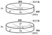
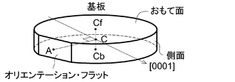
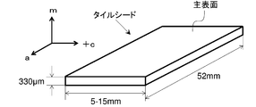
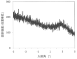
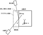
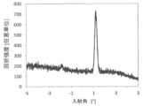
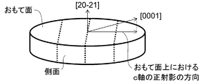
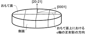
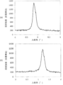
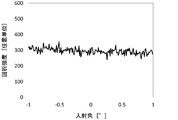
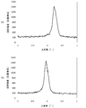
L'invention concerne un substrat en GaN, non polaire ou semi-polaire, présentant un diamètre de 2 pouces (environ 5 cm) ou plus, qui ne présente pas de parties dans lesquelles la cristallinité est réduite de manière significative au niveau des parties d'extrémité dans la direction orthogonale à l'axe c. Le substrat en GaN en forme de disque présentant un diamètre de 2 pouces (environ 5 cm) ou plus comprend une surface avant, qui présente, par rapport à un plan (0001), un angle d'inclinaison de 45° à 135° et une direction d'inclinaison qui est une direction dans une plage de ± 5° centrée dans la direction <10-10>, et une surface arrière, qui est une surface principale sur le côté opposé de la surface avant. Le substrat en GaN en forme de disque présente, sur une surface latérale correspondante, un premier point qui est positionné dans une direction orthogonale à l'axe c lors de l'observation à partir du centre du substrat en GaN. Un pic de diffraction unique apparaît dans le diagramme de diffraction des rayons X obtenu lorsqu'un faisceau de rayons X (CuKα1 : longueur d'onde 0,1542 nm) est incident sur le premier point et qu'un balayage θ est effectué par le changement de l'angle d'incidence θ du faisceau incident de rayons X, tout en fixant l'angle 2θ du faisceau diffracté de rayons X au double de l'angle de Bragg 28,99° du plan {11-20}.
Priority Applications (2)
| Application Number | Priority Date | Filing Date | Title |
|---|---|---|---|
| JP2016512147A JP5950070B1 (ja) | 2014-12-16 | 2015-11-18 | GaN基板 |
| US15/625,019 US10612161B2 (en) | 2014-12-16 | 2017-06-16 | GaN substrate |
Applications Claiming Priority (6)
| Application Number | Priority Date | Filing Date | Title |
|---|---|---|---|
| JP2014254462 | 2014-12-16 | ||
| JP2014-254462 | 2014-12-16 | ||
| JP2015-010670 | 2015-01-22 | ||
| JP2015010670 | 2015-01-22 | ||
| JP2015140702 | 2015-07-14 | ||
| JP2015-140702 | 2015-07-14 |
Related Child Applications (1)
| Application Number | Title | Priority Date | Filing Date |
|---|---|---|---|
| US15/625,019 Continuation US10612161B2 (en) | 2014-12-16 | 2017-06-16 | GaN substrate |
Publications (1)
| Publication Number | Publication Date |
|---|---|
| WO2016098518A1 true WO2016098518A1 (fr) | 2016-06-23 |
Family
ID=56126416
Family Applications (1)
| Application Number | Title | Priority Date | Filing Date |
|---|---|---|---|
| PCT/JP2015/082439 WO2016098518A1 (fr) | 2014-12-16 | 2015-11-18 | SUBSTRAT EN GaN |
Country Status (3)
| Country | Link |
|---|---|
| US (1) | US10612161B2 (fr) |
| JP (2) | JP5950070B1 (fr) |
| WO (1) | WO2016098518A1 (fr) |
Cited By (2)
| Publication number | Priority date | Publication date | Assignee | Title |
|---|---|---|---|---|
| JP2019085290A (ja) * | 2017-11-06 | 2019-06-06 | 古河機械金属株式会社 | Iii族窒化物半導体基板 |
| WO2020241760A1 (fr) * | 2019-05-30 | 2020-12-03 | 三菱ケミカル株式会社 | Tranche de substrat de gan et son procédé de fabrication |
Families Citing this family (9)
| Publication number | Priority date | Publication date | Assignee | Title |
|---|---|---|---|---|
| US9564320B2 (en) | 2010-06-18 | 2017-02-07 | Soraa, Inc. | Large area nitride crystal and method for making it |
| KR102335452B1 (ko) * | 2015-06-16 | 2021-12-07 | 서울바이오시스 주식회사 | 발광 소자 |
| CN108922849B (zh) * | 2018-07-13 | 2019-07-12 | 苏州汉骅半导体有限公司 | 半导体结构制造方法 |
| US11466384B2 (en) | 2019-01-08 | 2022-10-11 | Slt Technologies, Inc. | Method of forming a high quality group-III metal nitride boule or wafer using a patterned substrate |
| US11195973B1 (en) * | 2019-05-17 | 2021-12-07 | Facebook Technologies, Llc | III-nitride micro-LEDs on semi-polar oriented GaN |
| US11175447B1 (en) | 2019-08-13 | 2021-11-16 | Facebook Technologies, Llc | Waveguide in-coupling using polarized light emitting diodes |
| US11721549B2 (en) | 2020-02-11 | 2023-08-08 | Slt Technologies, Inc. | Large area group III nitride crystals and substrates, methods of making, and methods of use |
| CN115104174A (zh) | 2020-02-11 | 2022-09-23 | Slt科技公司 | 改进的iii族氮化物衬底、制备方法和使用方法 |
| EP4104202A1 (fr) * | 2020-02-11 | 2022-12-21 | SLT Technologies, Inc. | Cristaux et substrats de nitrure du groupe iii de grande surface, leurs procédés de fabrication et leurs procédés d'utilisation |
Citations (2)
| Publication number | Priority date | Publication date | Assignee | Title |
|---|---|---|---|---|
| JP2011126749A (ja) * | 2009-12-18 | 2011-06-30 | Mitsubishi Chemicals Corp | Iii族窒化物結晶の製造方法及びiii族窒化物結晶 |
| JP2014028720A (ja) * | 2012-07-31 | 2014-02-13 | Mitsubishi Chemicals Corp | 第13族窒化物基板 |
Family Cites Families (12)
| Publication number | Priority date | Publication date | Assignee | Title |
|---|---|---|---|---|
| US7053413B2 (en) * | 2000-10-23 | 2006-05-30 | General Electric Company | Homoepitaxial gallium-nitride-based light emitting device and method for producing |
| JP4915128B2 (ja) | 2005-04-11 | 2012-04-11 | 日亜化学工業株式会社 | 窒化物半導体ウエハ及びその製造方法 |
| WO2007119433A1 (fr) * | 2006-03-20 | 2007-10-25 | Kanagawa Academy Of Science And Technology | Couche de nitrure de groupe iii-v et son procédé de fabrication |
| JP5332168B2 (ja) | 2006-11-17 | 2013-11-06 | 住友電気工業株式会社 | Iii族窒化物結晶の製造方法 |
| JP5040977B2 (ja) * | 2009-09-24 | 2012-10-03 | 住友電気工業株式会社 | 窒化物半導体基板、半導体装置およびそれらの製造方法 |
| JP5821164B2 (ja) * | 2010-04-27 | 2015-11-24 | 住友電気工業株式会社 | GaN基板および発光デバイス |
| US8253162B2 (en) | 2010-04-27 | 2012-08-28 | Sumitomo Electric Industries, Ltd. | GaN substrate and light-emitting device |
| US9564320B2 (en) * | 2010-06-18 | 2017-02-07 | Soraa, Inc. | Large area nitride crystal and method for making it |
| JP5808208B2 (ja) * | 2011-09-15 | 2015-11-10 | 株式会社サイオクス | 窒化物半導体基板の製造方法 |
| US8471366B2 (en) * | 2011-11-30 | 2013-06-25 | Sumitomo Electric Industries, Ltd. | Nitride semiconductor substrate |
| JP2014043388A (ja) * | 2012-07-31 | 2014-03-13 | Mitsubishi Chemicals Corp | 第13族窒化物結晶の製造方法 |
| JP2014118323A (ja) * | 2012-12-17 | 2014-06-30 | Mitsubishi Chemicals Corp | 周期表第13族金属窒化物半導体結晶の製造方法及び周期表第13族金属窒化物半導体結晶 |
-
2015
- 2015-11-18 JP JP2016512147A patent/JP5950070B1/ja active Active
- 2015-11-18 WO PCT/JP2015/082439 patent/WO2016098518A1/fr active Application Filing
-
2016
- 2016-05-25 JP JP2016104578A patent/JP6597481B2/ja active Active
-
2017
- 2017-06-16 US US15/625,019 patent/US10612161B2/en active Active
Patent Citations (2)
| Publication number | Priority date | Publication date | Assignee | Title |
|---|---|---|---|---|
| JP2011126749A (ja) * | 2009-12-18 | 2011-06-30 | Mitsubishi Chemicals Corp | Iii族窒化物結晶の製造方法及びiii族窒化物結晶 |
| JP2014028720A (ja) * | 2012-07-31 | 2014-02-13 | Mitsubishi Chemicals Corp | 第13族窒化物基板 |
Cited By (4)
| Publication number | Priority date | Publication date | Assignee | Title |
|---|---|---|---|---|
| JP2019085290A (ja) * | 2017-11-06 | 2019-06-06 | 古河機械金属株式会社 | Iii族窒化物半導体基板 |
| JP7084123B2 (ja) | 2017-11-06 | 2022-06-14 | 古河機械金属株式会社 | Iii族窒化物半導体基板 |
| WO2020241760A1 (fr) * | 2019-05-30 | 2020-12-03 | 三菱ケミカル株式会社 | Tranche de substrat de gan et son procédé de fabrication |
| CN113906169A (zh) * | 2019-05-30 | 2022-01-07 | 三菱化学株式会社 | GaN基板晶片及其制造方法 |
Also Published As
| Publication number | Publication date |
|---|---|
| US20170362739A1 (en) | 2017-12-21 |
| JP5950070B1 (ja) | 2016-07-13 |
| JPWO2016098518A1 (ja) | 2017-04-27 |
| JP6597481B2 (ja) | 2019-10-30 |
| US10612161B2 (en) | 2020-04-07 |
| JP2017019709A (ja) | 2017-01-26 |
Similar Documents
| Publication | Publication Date | Title |
|---|---|---|
| JP6597481B2 (ja) | GaN基板 | |
| US10301745B2 (en) | Large area, low-defect gallium-containing nitride crystals, method of making, and method of use | |
| US10655244B2 (en) | GaN substrate, method for producing GaN substrate, method for producing GaN crystal, and method for manufacturing semiconductor device | |
| JP7347555B2 (ja) | 導電性C面GaN基板 | |
| US8536030B2 (en) | Semipolar semiconductor crystal and method for manufacturing the same | |
| CN109563641B (zh) | GaN结晶生长方法和C面GaN基板 | |
| JP6292080B2 (ja) | 非極性または半極性GaN基板 | |
| JP6885547B2 (ja) | GaN結晶の製造方法 | |
| JP2010168273A (ja) | Iii族窒化物半導体の製造方法、およびテンプレート基板 | |
| JP6759831B2 (ja) | C面GaN基板 | |
| JP7074168B2 (ja) | C面GaN基板 | |
| WO2021002349A1 (fr) | Cristal de gan en vrac, tranche de gan à plan c et procédé de fabrication de cristal de gan en vrac | |
| US11236439B2 (en) | Non-polar or semi-polar GaN wafer | |
| WO2023190969A1 (fr) | CRISTAL DE GaN ET TRANCHE DE GaN | |
| JP2019077601A (ja) | Iii族窒化物半導体基板、及び、iii族窒化物半導体基板の製造方法 | |
| JP2017088430A (ja) | GaNウエハ |
Legal Events
| Date | Code | Title | Description |
|---|---|---|---|
| ENP | Entry into the national phase |
Ref document number: 2016512147 Country of ref document: JP Kind code of ref document: A |
|
| 121 | Ep: the epo has been informed by wipo that ep was designated in this application |
Ref document number: 15869726 Country of ref document: EP Kind code of ref document: A1 |
|
| NENP | Non-entry into the national phase |
Ref country code: DE |
|
| 122 | Ep: pct application non-entry in european phase |
Ref document number: 15869726 Country of ref document: EP Kind code of ref document: A1 |