WO2016086484A1 - 一种低温多晶硅薄膜晶体管及其制造方法 - Google Patents
一种低温多晶硅薄膜晶体管及其制造方法 Download PDFInfo
- Publication number
- WO2016086484A1 WO2016086484A1 PCT/CN2014/095567 CN2014095567W WO2016086484A1 WO 2016086484 A1 WO2016086484 A1 WO 2016086484A1 CN 2014095567 W CN2014095567 W CN 2014095567W WO 2016086484 A1 WO2016086484 A1 WO 2016086484A1
- Authority
- WO
- WIPO (PCT)
- Prior art keywords
- layer
- doped
- forming
- amorphous silicon
- drain terminal
- Prior art date
- Legal status (The legal status is an assumption and is not a legal conclusion. Google has not performed a legal analysis and makes no representation as to the accuracy of the status listed.)
- Ceased
Links
Images


Classifications
-
- H—ELECTRICITY
- H10—SEMICONDUCTOR DEVICES; ELECTRIC SOLID-STATE DEVICES NOT OTHERWISE PROVIDED FOR
- H10D—INORGANIC ELECTRIC SEMICONDUCTOR DEVICES
- H10D30/00—Field-effect transistors [FET]
- H10D30/01—Manufacture or treatment
- H10D30/021—Manufacture or treatment of FETs having insulated gates [IGFET]
- H10D30/031—Manufacture or treatment of FETs having insulated gates [IGFET] of thin-film transistors [TFT]
- H10D30/0312—Manufacture or treatment of FETs having insulated gates [IGFET] of thin-film transistors [TFT] characterised by the gate electrodes
- H10D30/0314—Manufacture or treatment of FETs having insulated gates [IGFET] of thin-film transistors [TFT] characterised by the gate electrodes of lateral top-gate TFTs comprising only a single gate
-
- H—ELECTRICITY
- H10—SEMICONDUCTOR DEVICES; ELECTRIC SOLID-STATE DEVICES NOT OTHERWISE PROVIDED FOR
- H10D—INORGANIC ELECTRIC SEMICONDUCTOR DEVICES
- H10D30/00—Field-effect transistors [FET]
- H10D30/01—Manufacture or treatment
- H10D30/021—Manufacture or treatment of FETs having insulated gates [IGFET]
- H10D30/022—Manufacture or treatment of FETs having insulated gates [IGFET] having lightly-doped source or drain extensions selectively formed at the sides of the gates
-
- H—ELECTRICITY
- H10—SEMICONDUCTOR DEVICES; ELECTRIC SOLID-STATE DEVICES NOT OTHERWISE PROVIDED FOR
- H10D—INORGANIC ELECTRIC SEMICONDUCTOR DEVICES
- H10D30/00—Field-effect transistors [FET]
- H10D30/01—Manufacture or treatment
- H10D30/021—Manufacture or treatment of FETs having insulated gates [IGFET]
- H10D30/031—Manufacture or treatment of FETs having insulated gates [IGFET] of thin-film transistors [TFT]
- H10D30/0321—Manufacture or treatment of FETs having insulated gates [IGFET] of thin-film transistors [TFT] comprising silicon, e.g. amorphous silicon or polysilicon
-
- H—ELECTRICITY
- H10—SEMICONDUCTOR DEVICES; ELECTRIC SOLID-STATE DEVICES NOT OTHERWISE PROVIDED FOR
- H10D—INORGANIC ELECTRIC SEMICONDUCTOR DEVICES
- H10D30/00—Field-effect transistors [FET]
- H10D30/60—Insulated-gate field-effect transistors [IGFET]
- H10D30/601—Insulated-gate field-effect transistors [IGFET] having lightly-doped drain or source extensions, e.g. LDD IGFETs or DDD IGFETs
-
- H—ELECTRICITY
- H10—SEMICONDUCTOR DEVICES; ELECTRIC SOLID-STATE DEVICES NOT OTHERWISE PROVIDED FOR
- H10D—INORGANIC ELECTRIC SEMICONDUCTOR DEVICES
- H10D30/00—Field-effect transistors [FET]
- H10D30/60—Insulated-gate field-effect transistors [IGFET]
- H10D30/67—Thin-film transistors [TFT]
-
- H—ELECTRICITY
- H10—SEMICONDUCTOR DEVICES; ELECTRIC SOLID-STATE DEVICES NOT OTHERWISE PROVIDED FOR
- H10D—INORGANIC ELECTRIC SEMICONDUCTOR DEVICES
- H10D30/00—Field-effect transistors [FET]
- H10D30/60—Insulated-gate field-effect transistors [IGFET]
- H10D30/67—Thin-film transistors [TFT]
- H10D30/6704—Thin-film transistors [TFT] having supplementary regions or layers in the thin films or in the insulated bulk substrates for controlling properties of the device
- H10D30/6713—Thin-film transistors [TFT] having supplementary regions or layers in the thin films or in the insulated bulk substrates for controlling properties of the device characterised by the properties of the source or drain regions, e.g. compositions or sectional shapes
- H10D30/6715—Thin-film transistors [TFT] having supplementary regions or layers in the thin films or in the insulated bulk substrates for controlling properties of the device characterised by the properties of the source or drain regions, e.g. compositions or sectional shapes characterised by the doping profiles, e.g. having lightly-doped source or drain extensions
- H10D30/6719—Thin-film transistors [TFT] having supplementary regions or layers in the thin films or in the insulated bulk substrates for controlling properties of the device characterised by the properties of the source or drain regions, e.g. compositions or sectional shapes characterised by the doping profiles, e.g. having lightly-doped source or drain extensions having significant overlap between the lightly-doped drains and the gate electrodes, e.g. gate-overlapped LDD [GOLDD] TFTs
-
- H—ELECTRICITY
- H10—SEMICONDUCTOR DEVICES; ELECTRIC SOLID-STATE DEVICES NOT OTHERWISE PROVIDED FOR
- H10D—INORGANIC ELECTRIC SEMICONDUCTOR DEVICES
- H10D30/00—Field-effect transistors [FET]
- H10D30/60—Insulated-gate field-effect transistors [IGFET]
- H10D30/67—Thin-film transistors [TFT]
- H10D30/6729—Thin-film transistors [TFT] characterised by the electrodes
- H10D30/673—Thin-film transistors [TFT] characterised by the electrodes characterised by the shapes, relative sizes or dispositions of the gate electrodes
- H10D30/6731—Top-gate only TFTs
-
- H—ELECTRICITY
- H10—SEMICONDUCTOR DEVICES; ELECTRIC SOLID-STATE DEVICES NOT OTHERWISE PROVIDED FOR
- H10D—INORGANIC ELECTRIC SEMICONDUCTOR DEVICES
- H10D30/00—Field-effect transistors [FET]
- H10D30/60—Insulated-gate field-effect transistors [IGFET]
- H10D30/67—Thin-film transistors [TFT]
- H10D30/674—Thin-film transistors [TFT] characterised by the active materials
- H10D30/6741—Group IV materials, e.g. germanium or silicon carbide
- H10D30/6743—Silicon
- H10D30/6745—Polycrystalline or microcrystalline silicon
-
- H—ELECTRICITY
- H10—SEMICONDUCTOR DEVICES; ELECTRIC SOLID-STATE DEVICES NOT OTHERWISE PROVIDED FOR
- H10D—INORGANIC ELECTRIC SEMICONDUCTOR DEVICES
- H10D62/00—Semiconductor bodies, or regions thereof, of devices having potential barriers
- H10D62/10—Shapes, relative sizes or dispositions of the regions of the semiconductor bodies; Shapes of the semiconductor bodies
-
- H—ELECTRICITY
- H10—SEMICONDUCTOR DEVICES; ELECTRIC SOLID-STATE DEVICES NOT OTHERWISE PROVIDED FOR
- H10D—INORGANIC ELECTRIC SEMICONDUCTOR DEVICES
- H10D62/00—Semiconductor bodies, or regions thereof, of devices having potential barriers
- H10D62/10—Shapes, relative sizes or dispositions of the regions of the semiconductor bodies; Shapes of the semiconductor bodies
- H10D62/13—Semiconductor regions connected to electrodes carrying current to be rectified, amplified or switched, e.g. source or drain regions
-
- H—ELECTRICITY
- H10—SEMICONDUCTOR DEVICES; ELECTRIC SOLID-STATE DEVICES NOT OTHERWISE PROVIDED FOR
- H10P—GENERIC PROCESSES OR APPARATUS FOR THE MANUFACTURE OR TREATMENT OF DEVICES COVERED BY CLASS H10
- H10P14/00—Formation of materials, e.g. in the shape of layers or pillars
- H10P14/20—Formation of materials, e.g. in the shape of layers or pillars of semiconductor materials
- H10P14/34—Deposited materials, e.g. layers
- H10P14/3451—Structure
- H10P14/3452—Microstructure
- H10P14/3454—Amorphous
-
- H—ELECTRICITY
- H10—SEMICONDUCTOR DEVICES; ELECTRIC SOLID-STATE DEVICES NOT OTHERWISE PROVIDED FOR
- H10P—GENERIC PROCESSES OR APPARATUS FOR THE MANUFACTURE OR TREATMENT OF DEVICES COVERED BY CLASS H10
- H10P14/00—Formation of materials, e.g. in the shape of layers or pillars
- H10P14/20—Formation of materials, e.g. in the shape of layers or pillars of semiconductor materials
- H10P14/38—Formation of materials, e.g. in the shape of layers or pillars of semiconductor materials characterised by treatments done after the formation of the materials
- H10P14/3802—Crystallisation or recrystallisation of non-monocrystalline semiconductor materials, e.g. regrowth
- H10P14/3808—Crystallisation or recrystallisation of non-monocrystalline semiconductor materials, e.g. regrowth using laser beams
-
- H—ELECTRICITY
- H10—SEMICONDUCTOR DEVICES; ELECTRIC SOLID-STATE DEVICES NOT OTHERWISE PROVIDED FOR
- H10P—GENERIC PROCESSES OR APPARATUS FOR THE MANUFACTURE OR TREATMENT OF DEVICES COVERED BY CLASS H10
- H10P34/00—Irradiation with electromagnetic or particle radiation of wafers, substrates or parts of devices
- H10P34/40—Irradiation with electromagnetic or particle radiation of wafers, substrates or parts of devices with high-energy radiation
- H10P34/42—Irradiation with electromagnetic or particle radiation of wafers, substrates or parts of devices with high-energy radiation with electromagnetic radiation, e.g. laser annealing
-
- H—ELECTRICITY
- H10—SEMICONDUCTOR DEVICES; ELECTRIC SOLID-STATE DEVICES NOT OTHERWISE PROVIDED FOR
- H10P—GENERIC PROCESSES OR APPARATUS FOR THE MANUFACTURE OR TREATMENT OF DEVICES COVERED BY CLASS H10
- H10P95/00—Generic processes or apparatus for manufacture or treatments not covered by the other groups of this subclass
- H10P95/90—Thermal treatments, e.g. annealing or sintering
-
- H—ELECTRICITY
- H10—SEMICONDUCTOR DEVICES; ELECTRIC SOLID-STATE DEVICES NOT OTHERWISE PROVIDED FOR
- H10P—GENERIC PROCESSES OR APPARATUS FOR THE MANUFACTURE OR TREATMENT OF DEVICES COVERED BY CLASS H10
- H10P14/00—Formation of materials, e.g. in the shape of layers or pillars
- H10P14/20—Formation of materials, e.g. in the shape of layers or pillars of semiconductor materials
- H10P14/24—Formation of materials, e.g. in the shape of layers or pillars of semiconductor materials using chemical vapour deposition [CVD]
-
- H—ELECTRICITY
- H10—SEMICONDUCTOR DEVICES; ELECTRIC SOLID-STATE DEVICES NOT OTHERWISE PROVIDED FOR
- H10P—GENERIC PROCESSES OR APPARATUS FOR THE MANUFACTURE OR TREATMENT OF DEVICES COVERED BY CLASS H10
- H10P14/00—Formation of materials, e.g. in the shape of layers or pillars
- H10P14/20—Formation of materials, e.g. in the shape of layers or pillars of semiconductor materials
- H10P14/34—Deposited materials, e.g. layers
- H10P14/3402—Deposited materials, e.g. layers characterised by the chemical composition
- H10P14/3404—Deposited materials, e.g. layers characterised by the chemical composition being Group IVA materials
- H10P14/3411—Silicon, silicon germanium or germanium
-
- H—ELECTRICITY
- H10—SEMICONDUCTOR DEVICES; ELECTRIC SOLID-STATE DEVICES NOT OTHERWISE PROVIDED FOR
- H10P—GENERIC PROCESSES OR APPARATUS FOR THE MANUFACTURE OR TREATMENT OF DEVICES COVERED BY CLASS H10
- H10P14/00—Formation of materials, e.g. in the shape of layers or pillars
- H10P14/20—Formation of materials, e.g. in the shape of layers or pillars of semiconductor materials
- H10P14/34—Deposited materials, e.g. layers
- H10P14/3438—Doping during depositing
- H10P14/3441—Conductivity type
- H10P14/3442—N-type
Definitions
- the invention belongs to the technical field of transistor manufacturing, and particularly relates to a method for manufacturing a low temperature polysilicon thin film transistor, and to a low temperature polysilicon thin film transistor.
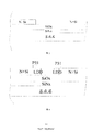
- FIG. 1 it is a prior art LTPS-TFT (Low Temperature).
- Poly-Silicon-Thin Film Transistor a schematic diagram of the structure of a low temperature polysilicon thin film transistor.
- a Substrate layer, a SiNx (silicon nitride) layer, and a SiOx (silicon oxide) layer are sequentially deposited to form a substrate layer, followed by deposition of an a-Si (amorphous silicon) layer, and a-Si is crystallized via Laser. It becomes a Poly-Si (polysilicon) film, and then a pattern layer structure is obtained by a yellow light/etching process.
- N+ (doped regions) and N- (LDD, lightly doped drain terminals) regions by yellow photoresist doping (mixed) in the N+ and N- regions Miscellaneous) different doses of P31 (phosphorus relative to molecular mass 31), ie, ion implantation of P31, yielding N-.
- the GI (silicon nitride) and GE (gate metal) layers, the Source (source metal) layer, the Drain (drain metal) layer, and the like shown in FIG. 1 are obtained by multiple deposition, yellow light, and etching.
- embodiments of the present invention provide a low temperature polysilicon thin film transistor and a method of fabricating the same to reduce the complexity of the process flow, reduce cost, and improve production efficiency.
- an embodiment of the present invention provides a method for fabricating a low temperature polysilicon thin film transistor, the method comprising: depositing a material comprising silane, phosphine, and hydrogen on a substrate layer to form an N+Si dopant.
- a hetero-layer and forming a first doped layer and a second doped layer by pattern etching; depositing an a-Si amorphous silicon layer on the N+Si doped layer, the a-Si amorphous silicon layer Performing a laser annealing, pattern etching process to form a portion of the a-Si amorphous silicon layer in the channel between the first doped layer and the second doped layer, and acting on the first doped layer by high temperature Forming a second lightly doped drain terminal between the portion of the a-Si amorphous silicon layer, the first lightly doped drain terminal, the first doped layer, and the portion of the a-Si amorphous silicon layer And forming a first phosphor material structure on the first doped layer and the first lightly doped drain terminal, and forming a second phosphor material structure on the second doped layer and the second lightly doped drain terminal; Forming a gate metal layer on the a-Si amorphous silicon layer and respectively
- first lightly doped drain terminal and the first phosphor material structure are formed by high temperature diffusion of a phosphor material of the first doped layer, the second lightly doped drain terminal and the second phosphor material
- the structure is formed by high temperature diffusion of the phosphor material of the second doped layer.
- excimer laser annealing is used.
- the a-Si amorphous silicon layer is subjected to laser crystallization to be converted into a Poly-Si film.
- the phosphor materials of the first doped layer and the second doped layer are formed by high-temperature diffusion in the direction of the Poly-Si film.
- the phosphorus material of the N+Si doped layer has a relative molecular mass of 31.
- the method further includes: controlling a mass fraction of the mass of the phosphine to control resistance values of the first lightly doped drain terminal and the second lightly doped drain terminal.
- etching is performed by yellow light irradiation.
- the step of performing laser annealing and pattern etching on the a-Si amorphous silicon layer includes performing dehydrogenation treatment on the a-Si amorphous silicon layer.
- an embodiment of the present invention further provides a low temperature polysilicon thin film transistor which is produced by any of the above manufacturing methods.
- the beneficial effects of the embodiments of the present invention are: the present invention automatically forms a lightly doped drain terminal and a phosphor material structure by diffusion by utilizing a phosphorus material contained in the N+Si doped layer by a high temperature action of laser annealing. Reduce the number of masks and simplify the production process. Compared with the prior art, the embodiment of the invention reduces the ion implantation process flow twice, reduces the number of times of using the mask, reduces the complexity of the process flow, reduces the cost, and improves the production efficiency.
- FIG. 1 is a partial schematic structural view of a prior art low temperature polysilicon thin film transistor
- FIG. 2 is a schematic flow chart of an embodiment of a method for fabricating a low temperature polysilicon thin film transistor of the present invention
- FIG. 6 is a partial structural view of the low-temperature polysilicon thin film transistor manufactured by the manufacturing method shown in FIG. 2.
- FIG. 2 is a schematic flow chart of an embodiment of a method for fabricating a low temperature polysilicon thin film transistor according to the present invention.
- the manufacturing method of the embodiment includes, but is not limited to, the following steps.
- step S100 an N+Si doped layer is deposited on the substrate layer by using a material comprising silane, phosphine and hydrogen, and the opposite first doped layer and the second doped layer are formed by pattern etching.
- the substrate layer of the present embodiment may include a substrate layer, a SiNx layer, and an SiOx layer, and the specific forming method and process flow can be obtained by the prior art method. It is not limited in the scope that the field personnel can easily understand.
- the silane described in this embodiment is SiH4, the phosphine is PH3, and the hydrogen is H2, which is the film forming gas used in the embodiment, and may of course include other materials. Further, the mass fraction between the silane, phosphine and hydrogen of the present embodiment can be adjusted according to the needs of the process flow.
- the pattern etching process of this embodiment may be irradiated and etched by a yellow light of the prior art, which will not be described in detail herein, and the first doped layer and the second doped layer are two spaced apart from each other as shown in FIG. N+Si.
- Step S101 depositing an a-Si amorphous silicon layer on the N+Si doped layer, performing laser annealing and pattern etching on the a-Si amorphous silicon layer to be in the first doped layer and a channel between the two doped layers forms a portion of the a-Si amorphous silicon layer, and forms a first lightly doped drain between the first doped layer and the portion of the a-Si amorphous silicon layer by high temperature action Forming a second lightly doped drain terminal between the first doped layer and the portion of the a-Si amorphous silicon layer, and forming a first layer on the first doped layer and the first lightly doped drain terminal A phosphor material structure, a second phosphor material structure is formed on the second doped layer and the second lightly doped drain terminal.
- the first lightly doped drain terminal LDD and the first phosphor material structure P31 are formed by high temperature diffusion of the phosphor material of the first doped layer N+Si, and the second lightly doped drain terminal LDD And the second phosphor material structure P31 is formed by high-temperature diffusion of the phosphor material of the second doped layer N+Si.
- the relative molecular mass of the phosphorus material of the N+Si doped layer of the present embodiment is 31. It should be noted that since the phosphorous material in N+Si is rapidly expanded under the condition of instantaneous high temperature, it is not necessary to adopt the prior art ion implantation process.
- the present embodiment preferably employs ELA (Excimer Laser). Annealer, excimer laser annealing) technology.
- ELA Excimer Laser
- the a-Si amorphous silicon layer is laser crystallized into a Poly-Si thin film (a structure between two LDDs), as shown in FIG. 4, the first doped layer and the second doped layer.
- the phosphor material of the layer is formed by high-temperature diffusion in the direction of the Poly-Si film to form the first and second lightly doped drain terminals LDD and the first and second phosphor material structures P31, respectively.
- the embodiment may specifically include a process flow for dehydrogenating the a-Si amorphous silicon layer.
- the present embodiment can control the resistance values of the first lightly doped drain terminal and the second lightly doped drain terminal by controlling the mass fraction of the quality of the phosphine.
- the present invention can appropriately adjust the concentration, volume, and the like formed at the time of high-temperature diffusion molding by controlling the mass fraction of the quality of the phosphine to obtain a preferable structure and performance.
- Step S102 forming a gate metal layer on the portion of the a-Si amorphous silicon layer, and respectively forming a source metal layer on the first doped layer on both sides of the gate metal layer, and in the second doping A drain metal layer is formed on the impurity layer.
- step S102 as shown in FIG. 5 and FIG. 6, respectively, a GI layer of SiNx and a GE layer of a metal material are formed to obtain a gate metal layer, and then an ILD layer formed of SiOx and SiNx may be formed (not shown). Etc., there is no limit here.
- the source metal layer is the Source layer shown in FIG. 6, and the drain metal layer is the Drain layer shown in FIG. 6.
- the high-temperature effect of laser annealing utilizes the phosphorus material contained in the N+Si doped layer to pass high temperature and diffusion.
- the first and second lightly doped drain terminals and the first and second phosphor materials are automatically formed, which can reduce the number of times of using the mask and simplify the manufacturing process.
- the embodiment of the invention reduces the ion implantation process flow twice, reduces the number of masks, reduces the complexity of the process flow, reduces the cost and improves the production efficiency.
- FIG. 6 is a low temperature polysilicon thin film transistor according to an embodiment of the present invention, which can be fabricated by the manufacturing method described in any of the preceding embodiments.
- the low temperature polysilicon thin film transistor includes, but is not limited to, a substrate layer (substrate layer, SiNx layer and SiOx layer which are sequentially stacked), oppositely disposed first doped layers N+Si and second doping.
- Layer N+Si first lightly doped drain terminal LDD and second lightly doped drain terminal LDD, first phosphor material structure P31 and second phosphor material structure P31, gate metal layer, source metal layer and drain metal Floor.
- the low temperature polysilicon thin film transistor of the embodiment can be used for an organic light emitting diode display.
- first and second lightly doped drain terminals LDD, and the first and second phosphor material structures P31 of the present embodiment are preferably formed by high-temperature diffusion of a phosphorus material contained in the N+Si doped layer. Simple and easy to manufacture, it reduces the number of ion implantation processes, reduces the number of times the mask is used, reduces the complexity of the process, reduces costs and increases productivity.
Landscapes
- Thin Film Transistor (AREA)
- Physics & Mathematics (AREA)
- Optics & Photonics (AREA)
- Electromagnetism (AREA)
Abstract
本发明实施例提供一种低温多晶硅薄膜晶体管及其制造方法,包括:在基材层上采用包括硅烷、磷化氢和氢气的材料沉积形成一N+Si掺杂层,并形成相对的第一掺杂层和第二掺杂层;在N+Si掺杂层上沉积一a-Si非晶硅层,对a-Si非晶硅层进行镭射退火、图形蚀刻处理,在第一掺杂层和第二掺杂层之间形成a-Si非晶硅层,且在第一掺杂层和a-Si非晶硅层之间形成第一轻掺杂漏极端、第一掺杂层和a-Si非晶硅层之间分别形成第二轻掺杂漏极端,以及在第一掺杂层和第一轻掺杂漏极端上形成第一磷材料结构、在第二掺杂层和第二轻掺杂漏极端上形成第二磷材料结构。本发明通过镭射退火的高温作用,利用N+Si掺杂层形成轻掺杂漏极端和磷材料结构,减少光罩的使用次数,简化制作工艺流程。
Description
【技术领域】
本发明属于晶体管制造技术领域,具体涉及一种低温多晶硅薄膜晶体管的制造方法,还涉及一种低温多晶硅薄膜晶体管。
【背景技术】
现有技术中,如图1所示,为现有技术的LTPS-TFT(Low Temperature
Poly-Silicon-Thin Film Transistor,低温多晶硅薄膜晶体管)的结构示意图。
从其结构中不难看出,其制造方法如下:
依序沉积Substrate(基底)层、SiNx(氮化硅)层、SiOx(氧化硅)层以形成基材层,接着沉积a-Si(非晶硅)层,a-Si经由Laser(镭射)结晶变为Poly-Si(多晶硅)薄膜,然后通过黄光/蚀刻制程得到图案图层结构。
接着,在图案图层上用两次Mask(镀膜)通过黄光光阻分别定义N+(掺杂区)和N-(LDD,轻掺杂漏极端)区域,其中,在N+和N-区域doping(掺杂)不同剂量的P31(相对分子质量为31的磷),即离子植入P31,得到N-。
通过多次沉积、黄光和蚀刻得到图1所示的GI(氮化硅)及GE(栅极金属)层、Source(源极金属)层和Drain(漏极金属)层等。
不难理解的是,现有技术需要通过反复多次沉积、黄光和刻蚀等工艺流程,增加了工艺流程的复杂度,制造成本高且生产效率均偏低。
【发明内容】
有鉴于此,本发明实施例提供一种低温多晶硅薄膜晶体管及其制造方法,以降低工艺流程的复杂度,降低成本并提高生产效率。
为解决上述技术问题,本发明实施例提供一种低温多晶硅薄膜晶体管的制造方法,所述制造方法包括:在基材层上采用包括硅烷、磷化氢和氢气的材料沉积形成一N+Si掺杂层,并通过图形蚀刻形成相对的第一掺杂层和第二掺杂层;在N+Si掺杂层上沉积一a-Si非晶硅层,对所述a-Si非晶硅层进行镭射退火、图形蚀刻处理,以在所述第一掺杂层和第二掺杂层之间的通道形成部分a-Si非晶硅层,且通过高温作用在所述第一掺杂层和所述部分a-Si非晶硅层之间形成第一轻掺杂漏极端、所述第一掺杂层和所述部分a-Si非晶硅层之间分别形成第二轻掺杂漏极端,以及在第一掺杂层和第一轻掺杂漏极端上形成第一磷材料结构、在第二掺杂层和第二轻掺杂漏极端上形成第二磷材料结构;在所述部分a-Si非晶硅层上制作栅极金属层,并分别在位于所述栅极金属层两侧的第一掺杂层上制作源极金属层、在第二掺杂层上制作漏极金属层。
其中,所述第一轻掺杂漏极端和所述第一磷材料结构经由所述第一掺杂层的磷材料高温扩散成型,所述第二轻掺杂漏极端和所述第二磷材料结构经由所述第二掺杂层的磷材料高温扩散成型。
其中,所述对所述a-Si非晶硅层进行镭射退火、图形蚀刻处理的步骤中,采用准分子镭射退火。
其中,所述对所述a-Si非晶硅层进行镭射退火、图形蚀刻处理的步骤中,对所述a-Si非晶硅层进行激光结晶转化为Poly-Si薄膜。
其中,所述第一掺杂层和所述第二掺杂层的磷材料往所述Poly-Si薄膜方向高温扩散成型。
其中,所述N+Si掺杂层的磷材料的相对分子质量为31。
其中,所述在基材层上采用包括硅烷、磷化氢和氢气的材料沉积形成一N+Si掺杂层,并通过图形蚀刻形成相对的第一掺杂层和第二掺杂层的步骤之前,还包括:控制所述磷化氢的质量所占的质量分数,以控制所述第一轻掺杂漏极端和所述第二轻掺杂漏极端的电阻值。
其中,所述通过图形蚀刻形成相对的第一掺杂层和第二掺杂层的步骤中,采用黄光照射蚀刻。
其中,所述对所述a-Si非晶硅层进行镭射退火、图形蚀刻处理的步骤中,包括对所述a-Si非晶硅层进行去氢处理。
为解决上述技术问题,本发明实施例还提供一种低温多晶硅薄膜晶体管,其采用任一上述的制造方法制得。
通过上述技术方案,本发明实施例的有益效果是:本发明通过镭射退火的高温作用,利用N+Si掺杂层含有的磷材料,通过扩散作用而自动形成轻掺杂漏极端和磷材料结构,减少光罩次数,简化制作工艺流程。相对于现有技术而言,本发明实施例减少两次的离子植入工艺流程,减少光罩的使用次数,降低工艺流程的复杂度,降低成本并提高生产效率。
【附图说明】
为了更清楚地说明本发明实施例中的技术方案,下面将对实施例描述中所需要使用的附图作简单地介绍,显而易见地,下面描述中的附图仅仅是本发明的一些实施例,对于本领域普通技术人员来讲,在不付出创造性劳动的前提下,还可以根据这些附图获得其他的附图。
图1是现有技术低温多晶硅薄膜晶体管的部分结构示意图;
图2是本发明低温多晶硅薄膜晶体管的制造方法一实施例的流程示意图;
图3到图6依序为图2所示制造方法的制造效果示意图,其中,图6为采用图2所示制造方法制造得到的低温多晶硅薄膜晶体管的部分结构示意图。
【具体实施方式】
下面将结合本发明实施例中的附图,对本发明实施例中的技术方案进行清楚、完整地描述,显然,本发明以下所描述的实施例仅仅是本发明的一部分实施例,而不是全部的实施例。基于本发明中的实施例,本领域普通技术人员在没有付出创造性劳动前提下所获得的所有其它实施例,都属于本发明保护的范围。
请参阅图2,图2是本发明低温多晶硅薄膜晶体管的制造方法一实施例的流程示意图,本实施例制造方法包括但不限于以下步骤。
步骤S100,在基材层上采用包括硅烷、磷化氢和氢气的材料沉积形成一N+Si掺杂层,并通过图形蚀刻形成相对的第一掺杂层和第二掺杂层。
在步骤S100中,如图3所示,本实施例的基材层可以包括substrate层、SiNx层和SiOx层,其具体形成方法和工艺流程,可以采用现有技术的方法制得,在本技术领域人员容易理解的范围内,不作限定。
不难理解的是,本实施例所述的硅烷为SiH4,磷化氢为PH3,氢气为H2,其为本实施例采用的成膜气体,当然,还可以包括其他材料。此外,本实施例的硅烷、磷化氢和氢气之间的质量分数可以根据工艺流程的需要而调整。
本实施例的图形蚀刻过程可以采用现有技术的黄光照射、蚀刻,在此不作细述,而第一掺杂层和第二掺杂层则为图3所示的彼此间隔成型的两个N+Si。
步骤S101,在N+Si掺杂层上沉积一a-Si非晶硅层,对所述a-Si非晶硅层进行镭射退火、图形蚀刻处理,以在所述第一掺杂层和第二掺杂层之间的通道形成部分a-Si非晶硅层,且通过高温作用在所述第一掺杂层和所述部分a-Si非晶硅层之间形成第一轻掺杂漏极端、所述第一掺杂层和所述部分a-Si非晶硅层之间分别形成第二轻掺杂漏极端,以及在第一掺杂层和第一轻掺杂漏极端上形成第一磷材料结构、在第二掺杂层和第二轻掺杂漏极端上形成第二磷材料结构。
值得注意的是,如图4所示,第一轻掺杂漏极端LDD和第一磷材料结构P31经由第一掺杂层N+Si的磷材料高温扩散成型,第二轻掺杂漏极端LDD和第二磷材料结构P31经由第二掺杂层N+Si的磷材料高温扩散成型。其中,不难理解的是,本实施例N+Si掺杂层的磷材料的相对分子质量为31。需要说明的是,由于N+Si里的磷材料在瞬间高温的状况下,其迅速进行扩展,而无需采用现有技术的离子植入的工艺流程。
其中,对a-Si非晶硅层进行镭射退火、图形蚀刻处理时,本实施例优选地采用ELA(Excimer Laser
Annealer,准分子镭射退火)技术。具体而言,本实施例对a-Si非晶硅层进行激光结晶转化为Poly-Si薄膜(两个LDD之间的结构),如图4所示,第一掺杂层和第二掺杂层的磷材料往Poly-Si薄膜方向高温扩散成型,以分别形成第一、第二轻掺杂漏极端LDD和第一、第二磷材料结构P31。
在上述镭射退火前,本实施例具体还可以包括对a-Si非晶硅层进行去氢处理的工艺流程。
需要说明的是,在步骤S100之前,本实施例可以通过控制磷化氢的质量所占的质量分数,以控制第一轻掺杂漏极端和第二轻掺杂漏极端的电阻值。换而言之,本发明通过控制磷化氢的质量所占的质量分数,使其高温扩散成型时所形成的浓度、体积等可以适当调整,以获得较佳的结构和性能。
步骤S102,在所述部分a-Si非晶硅层上制作栅极金属层,并分别在位于所述栅极金属层两侧的第一掺杂层上制作源极金属层、在第二掺杂层上制作漏极金属层。
在步骤S102中,如图5和图6所示,其分别制作SiNx的GI层和金属材料的GE层以得到栅极金属层,接着还可以制作SiOx和SiNx形成的ILD层(图未示)等,在此不作限定。
其中,源极金属层为图6所示的Source层,漏极金属层为图6所示的Drain层。
通过上述实施例描述的制造方法流程,不难看出,相对于现有技术而言,本发明实施例通过镭射退火的高温作用,利用N+Si掺杂层含有的磷材料,通过高温、扩散作用而自动形成第一、第二轻掺杂漏极端和第一、第二磷材料结构,可以减少光罩的使用次数,简化制作工艺流程。
本发明实施例减少两次的离子植入工艺流程,减少光罩次数,降低工艺流程的复杂度,降低成本并提高生产效率。
请参阅图6,为本发明实施例提供的一种低温多晶硅薄膜晶体管,其可以采用前面任一实施例所述的制造方法制得。
在本实施例中,低温多晶硅薄膜晶体管包括但不限于基材层(依序叠设成型的Substrate层、SiNx层和SiOx层)、相对设置的第一掺杂层N+Si和第二掺杂层N+Si、第一轻掺杂漏极端LDD和第二轻掺杂漏极端LDD、第一磷材料结构P31和第二磷材料结构P31、栅极金属层、源极金属层和漏极金属层。其中,其具体结构成型请参阅前面实施例的相关描述,在本技术领域人员容易结合理解的范围内,不作赘述。
其中,本实施例低温多晶硅薄膜晶体管可以用于有机发光二极管显示器。
同理,本实施例的第一、第二轻掺杂漏极端LDD,以及第一、第二磷材料结构P31,优选地采用N+Si掺杂层内含的磷材料高温扩散而成,结构简单且制造简便,能够减少两次的离子植入工艺流程,减少光罩的使用次数,降低工艺流程的复杂度,降低成本并提高生产效率。
以上所述仅为本发明的实施例,并非因此限制本发明的专利范围,凡是利用本发明说明书及附图内容所作的等效结构或等效流程变换,例如各实施例之间技术特征的相互结合,或直接或间接运用在其他相关的技术领域,均同理包括在本发明的专利保护范围内。
Claims (16)
- 一种低温多晶硅薄膜晶体管的制造方法,其中,所述制造方法包括:在基材层上采用包括硅烷、磷化氢和氢气的材料沉积形成一N+Si掺杂层,并通过图形蚀刻形成相对的第一掺杂层和第二掺杂层;在N+Si掺杂层上沉积一a-Si非晶硅层,对所述a-Si非晶硅层进行镭射退火、图形蚀刻处理,所述对所述a-Si非晶硅层进行镭射退火、图形蚀刻处理的步骤中,对所述a-Si非晶硅层进行激光结晶转化为Poly-Si薄膜,以在所述第一掺杂层和第二掺杂层之间的通道形成部分a-Si非晶硅层,且通过高温作用在所述第一掺杂层和所述部分a-Si非晶硅层之间形成第一轻掺杂漏极端、所述第一掺杂层和所述部分a-Si非晶硅层之间分别形成第二轻掺杂漏极端,以及在第一掺杂层和第一轻掺杂漏极端上形成第一磷材料结构、在第二掺杂层和第二轻掺杂漏极端上形成第二磷材料结构, 所述第一轻掺杂漏极端和所述第一磷材料结构经由所述第一掺杂层的磷材料高温扩散成型,所述第二轻掺杂漏极端和所述第二磷材料结构经由所述第二掺杂层的磷材料高温扩散成型;在所述部分a-Si非晶硅层上制作栅极金属层,并分别在位于所述栅极金属层两侧的第一掺杂层上制作源极金属层、在第二掺杂层上制作漏极金属层。
- 一种低温多晶硅薄膜晶体管的制造方法,其中,所述制造方法包括:在基材层上采用包括硅烷、磷化氢和氢气的材料沉积形成一N+Si掺杂层,并通过图形蚀刻形成相对的第一掺杂层和第二掺杂层;在N+Si掺杂层上沉积一a-Si非晶硅层,对所述a-Si非晶硅层进行镭射退火、图形蚀刻处理,以在所述第一掺杂层和第二掺杂层之间的通道形成部分a-Si非晶硅层,且通过高温作用在所述第一掺杂层和所述部分a-Si非晶硅层之间形成第一轻掺杂漏极端、所述第一掺杂层和所述部分a-Si非晶硅层之间分别形成第二轻掺杂漏极端,以及在第一掺杂层和第一轻掺杂漏极端上形成第一磷材料结构、在第二掺杂层和第二轻掺杂漏极端上形成第二磷材料结构;在所述部分a-Si非晶硅层上制作栅极金属层,并分别在位于所述栅极金属层两侧的第一掺杂层上制作源极金属层、在第二掺杂层上制作漏极金属层。
- 根据权利要求2所述的制造方法,其中,所述第一轻掺杂漏极端和所述第一磷材料结构经由所述第一掺杂层的磷材料高温扩散成型,所述第二轻掺杂漏极端和所述第二磷材料结构经由所述第二掺杂层的磷材料高温扩散成型。
- 根据权利要求3所述的制造方法,其中,所述对所述a-Si非晶硅层进行镭射退火、图形蚀刻处理的步骤中,采用准分子镭射退火。
- 根据权利要求2所述的制造方法,其中,所述对所述a-Si非晶硅层进行镭射退火、图形蚀刻处理的步骤中,对所述a-Si非晶硅层进行激光结晶转化为Poly-Si薄膜。
- 根据权利要求5所述的制造方法,其中,所述第一掺杂层和所述第二掺杂层的磷材料往所述Poly-Si薄膜方向高温扩散成型。
- 根据权利要求2所述的制造方法,其中,所述N+Si掺杂层的磷材料的相对分子质量为31。
- 根据权利要求2所述的制造方法,其中,所述在基材层上采用包括硅烷、磷化氢和氢气的材料沉积形成一N+Si掺杂层,并通过图形蚀刻形成相对的第一掺杂层和第二掺杂层的步骤之前,还包括:控制所述磷化氢的质量所占的质量分数,以控制所述第一轻掺杂漏极端和所述第二轻掺杂漏极端的电阻值。
- 根据权利要求3所述的制造方法,其中,所述在基材层上采用包括硅烷、磷化氢和氢气的材料沉积形成一N+Si掺杂层,并通过图形蚀刻形成相对的第一掺杂层和第二掺杂层的步骤之前,还包括:控制所述磷化氢的质量所占的质量分数,以控制所述第一轻掺杂漏极端和所述第二轻掺杂漏极端的电阻值。
- 根据权利要求4所述的制造方法,其中,所述在基材层上采用包括硅烷、磷化氢和氢气的材料沉积形成一N+Si掺杂层,并通过图形蚀刻形成相对的第一掺杂层和第二掺杂层的步骤之前,还包括:控制所述磷化氢的质量所占的质量分数,以控制所述第一轻掺杂漏极端和所述第二轻掺杂漏极端的电阻值。
- 根据权利要求5所述的制造方法,其中,所述在基材层上采用包括硅烷、磷化氢和氢气的材料沉积形成一N+Si掺杂层,并通过图形蚀刻形成相对的第一掺杂层和第二掺杂层的步骤之前,还包括:控制所述磷化氢的质量所占的质量分数,以控制所述第一轻掺杂漏极端和所述第二轻掺杂漏极端的电阻值。
- 根据权利要求6所述的制造方法,其中,所述在基材层上采用包括硅烷、磷化氢和氢气的材料沉积形成一N+Si掺杂层,并通过图形蚀刻形成相对的第一掺杂层和第二掺杂层的步骤之前,还包括:控制所述磷化氢的质量所占的质量分数,以控制所述第一轻掺杂漏极端和所述第二轻掺杂漏极端的电阻值。
- 根据权利要求7所述的制造方法,其中,所述在基材层上采用包括硅烷、磷化氢和氢气的材料沉积形成一N+Si掺杂层,并通过图形蚀刻形成相对的第一掺杂层和第二掺杂层的步骤之前,还包括:控制所述磷化氢的质量所占的质量分数,以控制所述第一轻掺杂漏极端和所述第二轻掺杂漏极端的电阻值。
- 根据权利要求2所述的制造方法,其中,所述通过图形蚀刻形成相对的第一掺杂层和第二掺杂层的步骤中,采用黄光照射蚀刻。
- 根据权利要求2所述的制造方法,其中,所述对所述a-Si非晶硅层进行镭射退火、图形蚀刻处理的步骤中,包括对所述a-Si非晶硅层进行去氢处理。
- 一种低温多晶硅薄膜晶体管,其中,其采用下述的制造方法制得,该制造方法包括:在基材层上采用包括硅烷、磷化氢和氢气的材料沉积形成一N+Si掺杂层,并通过图形蚀刻形成相对的第一掺杂层和第二掺杂层;在N+Si掺杂层上沉积一a-Si非晶硅层,对所述a-Si非晶硅层进行镭射退火、图形蚀刻处理,以在所述第一掺杂层和第二掺杂层之间的通道形成部分a-Si非晶硅层,且通过高温作用在所述第一掺杂层和所述部分a-Si非晶硅层之间形成第一轻掺杂漏极端、所述第一掺杂层和所述部分a-Si非晶硅层之间分别形成第二轻掺杂漏极端,以及在第一掺杂层和第一轻掺杂漏极端上形成第一磷材料结构、在第二掺杂层和第二轻掺杂漏极端上形成第二磷材料结构;在所述部分a-Si非晶硅层上制作栅极金属层,并分别在位于所述栅极金属层两侧的第一掺杂层上制作源极金属层、在第二掺杂层上制作漏极金属层。
Priority Applications (1)
| Application Number | Priority Date | Filing Date | Title |
|---|---|---|---|
| US14/426,247 US9685538B2 (en) | 2014-12-05 | 2014-12-30 | Low temperature polysilicon thin film transistor and method for fabricating same |
Applications Claiming Priority (2)
| Application Number | Priority Date | Filing Date | Title |
|---|---|---|---|
| CN201410737078.1A CN104465399B (zh) | 2014-12-05 | 2014-12-05 | 一种低温多晶硅薄膜晶体管及其制造方法 |
| CN201410737078.1 | 2014-12-05 |
Publications (1)
| Publication Number | Publication Date |
|---|---|
| WO2016086484A1 true WO2016086484A1 (zh) | 2016-06-09 |
Family
ID=52911257
Family Applications (1)
| Application Number | Title | Priority Date | Filing Date |
|---|---|---|---|
| PCT/CN2014/095567 Ceased WO2016086484A1 (zh) | 2014-12-05 | 2014-12-30 | 一种低温多晶硅薄膜晶体管及其制造方法 |
Country Status (3)
| Country | Link |
|---|---|
| US (1) | US9685538B2 (zh) |
| CN (1) | CN104465399B (zh) |
| WO (1) | WO2016086484A1 (zh) |
Families Citing this family (4)
| Publication number | Priority date | Publication date | Assignee | Title |
|---|---|---|---|---|
| CN105097550A (zh) * | 2015-08-04 | 2015-11-25 | 深圳市华星光电技术有限公司 | 低温多晶硅薄膜晶体管的制作方法及低温多晶硅薄膜晶体管 |
| CN105140128B (zh) * | 2015-09-08 | 2018-01-02 | 信利(惠州)智能显示有限公司 | 低温多晶硅薄膜晶体管及其制备方法 |
| CN105702622B (zh) * | 2016-02-01 | 2019-02-01 | 武汉华星光电技术有限公司 | 低温多晶硅tft基板的制作方法及低温多晶硅tft基板 |
| US10090415B1 (en) | 2017-11-29 | 2018-10-02 | International Business Machines Corporation | Thin film transistors with epitaxial source/drain contact regions |
Citations (4)
| Publication number | Priority date | Publication date | Assignee | Title |
|---|---|---|---|---|
| CN1525554A (zh) * | 2003-02-26 | 2004-09-01 | 友达光电股份有限公司 | 低温多晶硅薄膜晶体管的制作方法 |
| CN103000531A (zh) * | 2012-12-14 | 2013-03-27 | 友达光电股份有限公司 | 一种用于低温多晶硅薄膜晶体管的制造方法 |
| CN103839826A (zh) * | 2014-02-24 | 2014-06-04 | 京东方科技集团股份有限公司 | 一种低温多晶硅薄膜晶体管、阵列基板及其制作方法 |
| TW201448178A (zh) * | 2013-06-07 | 2014-12-16 | Everdisplay Optronics Shanghai Ltd | 薄膜電晶體和有源矩陣有機發光二極體組件及其製造方法 |
Family Cites Families (6)
| Publication number | Priority date | Publication date | Assignee | Title |
|---|---|---|---|---|
| US5913113A (en) * | 1997-02-24 | 1999-06-15 | Lg Electronics Inc. | Method for fabricating a thin film transistor of a liquid crystal display device |
| US20050191812A1 (en) * | 2004-03-01 | 2005-09-01 | Lsi Logic Corporation | Spacer-less transistor integration scheme for high-k gate dielectrics and small gate-to-gate spaces applicable to Si, SiGe strained silicon schemes |
| US20060060919A1 (en) * | 2004-09-21 | 2006-03-23 | Hsi-Ming Chang | Low temperature polysilicon thin film transistor and method of fabricating lightly doped drain thereof |
| KR101265331B1 (ko) * | 2006-06-28 | 2013-05-23 | 엘지디스플레이 주식회사 | 박막 트랜지스터, 그 제조방법, 이를 구비한 액정표시장치제조방법 |
| KR101206038B1 (ko) * | 2006-12-18 | 2012-11-28 | 삼성전자주식회사 | 박막 트랜지스터의 제조방법 |
| KR20110094837A (ko) * | 2010-02-18 | 2011-08-24 | 서울대학교산학협력단 | 박막 트랜지스터, 박막 트랜지스터의 제조 방법 및 이에 의한 박막 트랜지스터 |
-
2014
- 2014-12-05 CN CN201410737078.1A patent/CN104465399B/zh active Active
- 2014-12-30 US US14/426,247 patent/US9685538B2/en active Active
- 2014-12-30 WO PCT/CN2014/095567 patent/WO2016086484A1/zh not_active Ceased
Patent Citations (4)
| Publication number | Priority date | Publication date | Assignee | Title |
|---|---|---|---|---|
| CN1525554A (zh) * | 2003-02-26 | 2004-09-01 | 友达光电股份有限公司 | 低温多晶硅薄膜晶体管的制作方法 |
| CN103000531A (zh) * | 2012-12-14 | 2013-03-27 | 友达光电股份有限公司 | 一种用于低温多晶硅薄膜晶体管的制造方法 |
| TW201448178A (zh) * | 2013-06-07 | 2014-12-16 | Everdisplay Optronics Shanghai Ltd | 薄膜電晶體和有源矩陣有機發光二極體組件及其製造方法 |
| CN103839826A (zh) * | 2014-02-24 | 2014-06-04 | 京东方科技集团股份有限公司 | 一种低温多晶硅薄膜晶体管、阵列基板及其制作方法 |
Also Published As
| Publication number | Publication date |
|---|---|
| US20160343830A1 (en) | 2016-11-24 |
| CN104465399B (zh) | 2017-08-25 |
| US9685538B2 (en) | 2017-06-20 |
| CN104465399A (zh) | 2015-03-25 |
Similar Documents
| Publication | Publication Date | Title |
|---|---|---|
| WO2016074204A1 (zh) | 基于双栅极结构的低温多晶硅薄膜晶体管及其制备方法 | |
| US20180212061A1 (en) | Dual gate oxide thin-film transistor and manufacturing method for the same | |
| TW201330112A (zh) | 低溫多晶矽薄膜晶體管制造方法 | |
| WO2017219432A1 (zh) | 一种薄膜晶体管阵列基板及液晶面板 | |
| WO2016090689A1 (zh) | 一种阵列基板的掺杂方法及制造设备 | |
| WO2018035902A1 (zh) | 低温多晶硅阵列基板的制备方法、阵列基板以及显示面板 | |
| CN105448999B (zh) | 多晶硅薄膜晶体管元件及其制作方法 | |
| WO2016086484A1 (zh) | 一种低温多晶硅薄膜晶体管及其制造方法 | |
| CN107275390A (zh) | 薄膜晶体管及其制作方法、阵列基板及显示装置 | |
| CN107170759A (zh) | 一种阵列基板及其制作方法、显示装置 | |
| WO2015168961A1 (zh) | 薄膜晶体管阵列基板制造方法及薄膜晶体管阵列基板 | |
| CN105304641A (zh) | 一种低温多晶硅tft阵列基板的制造方法 | |
| WO2017000335A1 (zh) | Tft背板的制作方法及其结构 | |
| WO2014153841A1 (zh) | 低温多晶硅薄膜制作方法、薄膜晶体管制作方法 | |
| WO2019000508A1 (zh) | 薄膜晶体管阵列基板及其制备方法、显示装置 | |
| WO2016106923A1 (zh) | 一种ltps tft像素单元及其制造方法 | |
| TW200933892A (en) | Microcrystalline silicon thin film transistor and method for manufacturing the same | |
| WO2017152522A1 (zh) | 金属氧化物薄膜晶体管及其制作方法、阵列基板 | |
| WO2019100428A1 (zh) | 一种阵列基板及其制备方法 | |
| CN106783734B (zh) | 一种低温多晶硅阵列基板及其制作方法 | |
| WO2019056447A1 (zh) | 一种阵列基板及其制造方法 | |
| US20190221672A1 (en) | Low temperature polysilicon thin film transistor and preparation method thereof | |
| WO2019028934A1 (zh) | 低温多晶硅薄膜晶体管及其制备方法 | |
| WO2014201715A1 (zh) | 薄膜晶体管阵列基板及其沟道形成方法 | |
| WO2017096660A1 (zh) | 与数据线导通的薄膜晶体管的制备方法及薄膜晶体管 |
Legal Events
| Date | Code | Title | Description |
|---|---|---|---|
| WWE | Wipo information: entry into national phase |
Ref document number: 14426247 Country of ref document: US |
|
| 121 | Ep: the epo has been informed by wipo that ep was designated in this application |
Ref document number: 14907404 Country of ref document: EP Kind code of ref document: A1 |
|
| NENP | Non-entry into the national phase |
Ref country code: DE |
|
| 122 | Ep: pct application non-entry in european phase |
Ref document number: 14907404 Country of ref document: EP Kind code of ref document: A1 |