WO2016079798A1 - クロック伝送回路および半導体集積回路 - Google Patents
クロック伝送回路および半導体集積回路 Download PDFInfo
- Publication number
- WO2016079798A1 WO2016079798A1 PCT/JP2014/080472 JP2014080472W WO2016079798A1 WO 2016079798 A1 WO2016079798 A1 WO 2016079798A1 JP 2014080472 W JP2014080472 W JP 2014080472W WO 2016079798 A1 WO2016079798 A1 WO 2016079798A1
- Authority
- WO
- WIPO (PCT)
- Prior art keywords
- clock
- buffer
- inductor
- wiring
- transmission circuit
- Prior art date
- Legal status (The legal status is an assumption and is not a legal conclusion. Google has not performed a legal analysis and makes no representation as to the accuracy of the status listed.)
- Ceased
Links
Images



Classifications
-
- H—ELECTRICITY
- H03—ELECTRONIC CIRCUITRY
- H03K—PULSE TECHNIQUE
- H03K5/00—Manipulating of pulses not covered by one of the other main groups of this subclass
- H03K5/15—Arrangements in which pulses are delivered at different times at several outputs, i.e. pulse distributors
- H03K5/15013—Arrangements in which pulses are delivered at different times at several outputs, i.e. pulse distributors with more than two outputs
- H03K5/15026—Arrangements in which pulses are delivered at different times at several outputs, i.e. pulse distributors with more than two outputs with asynchronously driven series connected output stages
- H03K5/15033—Arrangements in which pulses are delivered at different times at several outputs, i.e. pulse distributors with more than two outputs with asynchronously driven series connected output stages using a chain of bistable devices
-
- G—PHYSICS
- G06—COMPUTING OR CALCULATING; COUNTING
- G06F—ELECTRIC DIGITAL DATA PROCESSING
- G06F1/00—Details not covered by groups G06F3/00 - G06F13/00 and G06F21/00
- G06F1/04—Generating or distributing clock signals or signals derived directly therefrom
- G06F1/10—Distribution of clock signals, e.g. skew
-
- G—PHYSICS
- G06—COMPUTING OR CALCULATING; COUNTING
- G06F—ELECTRIC DIGITAL DATA PROCESSING
- G06F1/00—Details not covered by groups G06F3/00 - G06F13/00 and G06F21/00
- G06F1/26—Power supply means, e.g. regulation thereof
- G06F1/266—Arrangements to supply power to external peripherals either directly from the computer or under computer control, e.g. supply of power through the communication port, computer controlled power-strips
-
- H—ELECTRICITY
- H04—ELECTRIC COMMUNICATION TECHNIQUE
- H04L—TRANSMISSION OF DIGITAL INFORMATION, e.g. TELEGRAPHIC COMMUNICATION
- H04L25/00—Baseband systems
- H04L25/02—Details ; arrangements for supplying electrical power along data transmission lines
-
- H—ELECTRICITY
- H04—ELECTRIC COMMUNICATION TECHNIQUE
- H04L—TRANSMISSION OF DIGITAL INFORMATION, e.g. TELEGRAPHIC COMMUNICATION
- H04L25/00—Baseband systems
- H04L25/02—Details ; arrangements for supplying electrical power along data transmission lines
- H04L25/03—Shaping networks in transmitter or receiver, e.g. adaptive shaping networks
Definitions
- the embodiment referred to in this application relates to a clock transmission circuit and a semiconductor integrated circuit.
- the clock transmission circuit is used to transmit a clock used in a semiconductor integrated circuit (LSI) from a clock oscillation source to each circuit block using the clock.
- Various clock signals such as a communication LSI and CPU are used. Widely used in various LSIs.
- the clock transmission circuit transmits the clock from the clock oscillation source to each circuit block while maintaining the waveform via a plurality of buffers.
- clock transmission by the clock transmission circuit is performed by applying, for example, a CMOS inverter or CML (Current Mode Logic).
- CMOS inverter or CML (Current Mode Logic)
- the load capacitance is charged and discharged, resulting in an increase in current consumption.
- the current consumption is proportional to the load capacity and the frequency.
- the frequency of internal clocks in LSIs has increased to several GHz or more with the increase in CPU processing speed and communication speed.
- the current consumption is proportional to the frequency, when the frequency of the internal clock increases to several GHz or more, an increase in the current consumption due to the clock transmission circuit has become a problem.
- inductor peaking resonant clock distribution
- the inductor peaking is also referred to as clock transmission by resonance.
- Inductor peaking is, for example, a technique of increasing the impedance viewed from the buffer of the clock transmission circuit by arranging an inductor in parallel with the load capacity and performing a clock transmission with a small load capacity.
- a device that performs clock transmission using inductor peaking has been proposed.
- a common voltage bias voltage
- a high resistance bias for example, a common voltage (bias voltage) is applied with a high resistance bias.
- a capacitive or resistive element is attached to a signal line that transmits a high-speed signal (clock) by an operational amplifier or a resistor. Has been done.
- the impedance when the impedance is increased, for example, it becomes easy to be affected by external noise, and jitter is generated in the transmitted clock or the duty ratio is shifted due to noise of the common voltage.
- a clock transmission circuit having a first buffer, a second buffer, and an inductor unit is provided.
- the first buffer receives one of the first clocks of the differential clock, buffers it, and outputs it to the first clock line.
- the second buffer receives the other second clock of the differential clock, buffers it, and outputs it to the second clock wiring.
- the inductor section is connected between a first node in the first clock line and a second node in the second clock line, and a common voltage is applied to the intermediate tap.
- the disclosed clock transmission circuit and semiconductor integrated circuit have an effect of stably transmitting a clock while suppressing a decrease in transmission band.
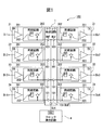
- FIG. 1 is a block diagram illustrating an example of a semiconductor integrated circuit to which a clock transmission circuit is applied.
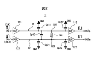
- FIG. 2 is a diagram for explaining an example of the clock transmission circuit shown in FIG.
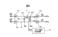
- FIG. 3 is a diagram for explaining application of a common voltage in the clock transmission circuit shown in FIG.
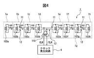
- FIG. 4 is a diagram for explaining another example of the clock transmission circuit shown in FIG.
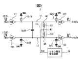
- FIG. 5 is a block diagram showing a first embodiment of the clock transmission circuit.
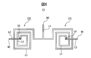
- FIG. 6 is a diagram for explaining an example of an inductor applied to the clock transmission circuit shown in FIG.
- FIG. 7 is a block diagram showing a second embodiment of the clock transmission circuit.
- FIG. 8 is a diagram for explaining an example of an inductor applied to the clock transmission circuit shown in FIG. FIG.
- FIG. 9 is a diagram for explaining an example of the common voltage generation circuit in the clock transmission circuit shown in FIG.
- FIG. 10 is a block diagram showing a third embodiment of the clock transmission circuit.
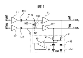
- FIG. 11 is a block diagram showing a fourth embodiment of the clock transmission circuit.
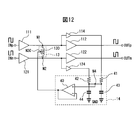
- FIG. 12 is a block diagram showing a fifth embodiment of the clock transmission circuit.
- FIG. 13 is a block diagram showing an example of a semiconductor integrated circuit to which the clock transmission circuit of this embodiment is applied.
- FIG. 1 is a block diagram showing an example of a semiconductor integrated circuit to which a clock transmission circuit is applied, and shows an example of a semiconductor integrated circuit for communication (communication LSI).
- a communication LSI 100 includes a clock transmission circuit 1, a plurality of data reception circuits (RX) 21 to 24, a plurality of data transmission circuits (TX) 31 to 34, and a clock generation circuit (clock oscillation source: Including oscillator OSC) 4.
- the clock generation circuit 4 generates a clock CLK by, for example, a PLL (Phase Locked Loop) and inputs it to the clock transmission circuit 1.
- the clock transmission circuit 1 includes a plurality of buffers (BUF) 101, and transmits the clock CLK to the data reception circuits 21 to 24 and the data transmission circuits 31 to 34 via the buffers 101.
- BAF buffers
- the data receiving circuit 21 (21 to 24) has the same configuration, and includes, for example, a buffer 201, a flip-flop (FF) 202, and a switch 203.
- the clock CLK from the clock transmission circuit 1 is used, for example, as a control signal for the flip-flop 202 and the switch 203 that form a synchronous circuit.
- the data receiving circuits 21 to 24 receive the input data (received signals) Di1 to Di4 and amplify them by the buffer 201, and reproduce the received signals Di1 to Di4 by the synchronizing circuit of the flip-flop 202 and the switch 203 based on the clock CLK. To do.
- the data transmission circuit 31 (31 to 34) has the same configuration, and includes, for example, an amplifier 301, a flip-flop 302 (FF), and a switch 303.
- the clock CLK from the clock transmission circuit 1 is used, for example, as a control signal for the flip-flop 302 and the switch 303 that form a synchronous circuit.
- the data transmission circuits 31 to 34 are processed by the synchronizing circuit of the flip-flop 302 and the switch 303 based on the clock CLK, and then amplified by the amplifier 301 to output output data (transmission signals) Do1 to Do4.
- the clock transmission circuit 1 sends the clock CLK from the clock generation circuit 4 to each of the data reception circuits 21 to 24 (202, 203) and each of the data transmission circuits 31 to 34 (302, 303) that use the clock. To transmit.
- FIG. 1 schematically illustrates the communication LSI 100.
- the clock CLK from the clock transmission circuit 1 is not limited to flip-flops and switches in the data reception circuit and the data transmission circuit, but is various. It is transmitted to the circuit block.
- FIG. 2 is a diagram for explaining an example of the clock transmission circuit shown in FIG. 1, and shows an example of the clock transmission circuit that performs clock transmission by applying inductor peaking.
- reference numerals 11 and 12 denote wirings (clock wirings)
- 111, 112, 121, and 122 denote buffers (BUF)
- 103 denotes an inductor
- Cp11, Cp12, Cp21, Cp22, and Cp30 Indicates parasitic capacitance.
- inductor peaking is a technique for performing clock transmission by increasing the impedance viewed from the buffer of the clock transmission circuit by, for example, arranging an inductor in parallel with the load capacitance and performing parallel resonance.
- the clock transmission circuit 1 receives differential (complementary) clocks CLK and / CLK at input terminals INp and INm, and includes buffers 111 and 112, clock wirings 11 and 12, and buffers 121 and 122, respectively. Via the output terminals OUTp and OUTm.
- capacitances (parasitic capacitances) Cp11 and Cp12 exist between the clock wiring 11 and the ground (ground) GND
- capacitances Cp21 and Cp22 exist between the clock wiring 12 and the ground GND
- a capacitance Cp30 exists between the clock wirings 11 and 12.
- the capacitor Cp30 is not a parasitic capacitor between the clock wirings 11 and 12, but may be a capacitor provided intentionally.
- the inductor 103 is connected to a node N11 of the clock wiring 11 between the buffers 111 and 112 that transmits the positive logic clock CLK and a node N21 of the clock wiring 12 between the buffers 121 and 122 that transmit the negative logic clock / CLK. It is connected.
- the load capacitance (parasitic capacitances Cp11, Cp12, Cp21, Cp22, Cp30) is caused to resonate in parallel, for example, the load capacitance seen from the buffers 111 and 121 is large. It seems to look small.
- the inductor 103 having the optimum inductance L between the clock wirings 11 and 12, for example, the sizes of the buffers 111 and 121 in the previous stage can be reduced, and current consumption can be reduced. It becomes.
- L 0.1 ⁇ H, which is difficult to realize in the chip.
- FIG. 3 is a diagram for explaining application of a common voltage in the clock transmission circuit shown in FIG.
- the load capacitances parasite capacitances Cp11, Cp12, Cp21, Cp22, Cp30
- the clock transmission circuit 1 shown in FIG. 3 generates resistors 151 and 152 provided in series between the clock wirings 11 and 12 and a common voltage Vcm.
- the common voltage generation circuit 14 is included.
- One end of the resistor 151 is connected to the node N11 of the clock line 11, one end of the resistor 152 is connected to the node N21 of the clock line 12, and the other ends of the resistors 151 and 152 are commonly connected at the node N300. Yes.
- the common voltage Vcm from the common voltage generation circuit 14 is applied to the common connection node N300 of the resistors 151 and 152.
- the clock transmission circuit shown in FIG. 3 is a technique of biasing (setting the common voltage by increasing the impedance) through the high-resistance elements (151 and 152: for example, several tens K ⁇ to several hundreds K ⁇ ). Is equivalent to the one applied.
- the high resistance element is formed on the semiconductor chip, for example, it is unavoidable to add a parasitic capacitance of several fF to several hundred fF, and the bandwidth of the clock transmission circuit is not avoided. Will be reduced.
- the impedance when the impedance is increased, for example, it becomes easy to be affected by external noise, and jitter is generated in the transmitted clock or the duty ratio is shifted due to noise of the common voltage.
- FIG. 4 is a diagram for explaining another example of the clock transmission circuit shown in FIG.
- the clock transmission circuit 1 includes, for example, buffering (for example, waveform shaping and amplification) the differential clocks CLK and / CLK from the clock generation circuit 4 with a buffer (BUF) 110. Transmit to circuits 1a-1h.
- buffering for example, waveform shaping and amplification
- inductors 103a to 103h are respectively provided for the plurality of internal circuits 1a to 1h (for example, the data transmission circuit TX) in the clock wirings 11 and 12 for transmitting the differential clocks CLK and / CLK. It is designed to be provided.
- the internal circuit 1h may be a dummy circuit of a data transmission circuit, for example.
- FIG. 5 is a block diagram showing a first embodiment of the clock transmission circuit.
- the clock transmission circuit 1 of the first embodiment has the inductors 131 and 132 in which the common voltage Vcm is provided in series between the clock wires 11 and 12. To the connection node N3.
- one first clock CLK of the differential clock is input from the input terminal INp to the first buffer 111, buffered (for example, waveform shaping and amplification), and passed through the first clock wiring 11 and the third buffer 112. And output from the output terminal OUTp.
- the other second clock / CLK of the differential clock is input from the input terminal INm to the second buffer 121, buffered, and output from the output terminal OUTm via the second clock line 12 and the fourth buffer 122.
- the inductor unit 13 includes a first inductor 131 and a second inductor 132, one end of the first inductor 131 is connected to the first node N1 of the first clock wiring 11, and one end of the second inductor 132 is the second inductor.
- the clock line 12 is connected to the second node N2.
- the other end of the first inductor 131 and the other end of the second inductor 132 are commonly connected at the third node N3, and the common voltage Vcm generated by the common voltage generation circuit 14 is applied to the third node N3. It has become so.
- first inductor 131 and the second inductor 132 have the same inductance.
- reference symbols Cp11, Cp12, Cp21, Cp22, and Cp30 indicate parasitic capacitances (load capacitances).
- the capacitor Cp30 may be a capacitor provided intentionally instead of a parasitic capacitor between the clock wirings 11 and 12.
- the inductors 131 and 132 are arranged in parallel with the load capacitances (Cp11, Cp12, Cp21, Cp22, and Cp30) and resonated in parallel, thereby performing inductor peaking that increases the impedance viewed from the buffers 111 and 121 of the clock transmission circuit 1. Use it to transmit the clock.
- the common voltage Vcm for bias application generated by the common voltage generation circuit 14 is applied to the common connection node N3 of the inductors 131 and 132 having the same inductance.
- the node N3 becomes the differential center of the differential clocks CLK and / CLK, the differential signal does not appear, and the transmitted differential clocks CLK, / CLK can be prevented from being adversely affected.
- the occurrence of jitter and the duty can be reduced without using a high resistance element as described with reference to FIG. 3 and without reducing the bandwidth of the clock transmission circuit.
- Stable clock transmission can be performed while suppressing the ratio deviation.
- FIG. 6 is a diagram for explaining an example of an inductor applied to the clock transmission circuit shown in FIG.
- reference numeral L1 indicates, for example, a first conductive layer (metal layer) in a semiconductor chip (semiconductor substrate, die), and L2 indicates a second conductive layer on the conductive layer L1.
- Reference numerals V1 and V2 indicate vias (contact holes) that electrically connect the first conductive layer L1 and the second conductive layer L2.
- the inductor section 13 in the clock transmission circuit of the first embodiment has two inductors 131 and 132.
- the first inductor 131 and the second inductor 132 are provided in a semiconductor chip. It is formed to have a symmetrical structure.
- the node N3 since the differential signals (clocks CLK and / CLK) are input to the nodes N1 and N2 of the two inductors 131 and 132 having the same inductance with a symmetrical structure, the node N3 has a differential center. It becomes. A bias due to the common voltage Vcm is applied to the node N3 at the differential center.
- the first clock wiring 11 is connected to, for example, an end portion (first node N1) of the second conductive layer L2 in the first inductor 131, and the second clock wiring 12 is connected to, for example, the second inductor 132.
- first node N1 an end portion of the second conductive layer L2 in the first inductor 131
- second clock wiring 12 is connected to, for example, the second inductor 132.
- second node N2 To the end of the second conductive layer L2 (second node N2).
- the common voltage Vcm generated by the common voltage generation circuit 14 is applied to, for example, the node N3 formed by the first conductive layer L1.
- the inductor unit 13 shown in FIG. 6 is merely an example, and various modifications and changes can be made.
- FIG. 7 is a block diagram showing a second embodiment of the clock transmission circuit
- FIG. 8 is a diagram for explaining an example of an inductor (common inductor 130) applied to the clock transmission circuit shown in FIG. .
- the load capacitors Cp11, Cp12, Cp21, Cp22, and Cp30 shown in FIG. 5 are omitted, and the omission of the load capacitors is the same in FIGS. 9 to 13 described later.
- reference numeral L1 indicates, for example, a first conductive layer in the semiconductor chip
- L2 indicates a second conductive layer on the conductive layer L1
- L3 indicates on the conductive layer L2.
- the third conductive layer is shown.
- V11, V12, V21, and V22 denote vias connecting the first conductive layer L1 and the second conductive layer L2, and V30 denotes the first conductive layer L1 and the third conductive layer.
- a via connecting L3 is shown.
- the inductor section 13 has an intermediate tap (center tap: third node) N30.
- One inductor (common inductor) 130 is used.
- the first inductor 131 in FIG. 5 corresponds to between the first node N 1 of the first clock line 11 and the intermediate tap N 30, and the second inductor 132 in FIG. 5 corresponds to the second clock line 12. Corresponds to between the second node N2 and the intermediate tap N30.
- the inductor corresponding to the first node N1 to the intermediate tap N30 and the inductor corresponding to the second node N2 to the intermediate tap N30 have the same inductance. .
- the inductor unit 13 formed by one common inductor 130 having the intermediate tap N30 is formed rather than the two inductors 131 and 132 formed.
- the occupied area can be reduced.
- the inductor unit 13 in the clock transmission circuit of the second embodiment has one common inductor 130, and the portions corresponding to the first and second inductors 131 and 132 described above are as follows.
- the semiconductor chip has a symmetrical structure.
- the node N30 is It becomes the differential center.
- a bias due to the common voltage Vcm is applied to the node N30 at the differential center.
- first clock line 11 is connected to, for example, one end (first node N1) of the first conductive layer L1 in the common inductor 130
- second clock line 12 is connected to, for example, the first layer in the common inductor 130.
- second node N2 Connected to the other end (second node N2) of the conductive layer L1.
- the common voltage Vcm generated by the common voltage generation circuit 14 is applied to, for example, the node N30 formed by the third conductive layer L3.
- the inductor section 13 shown in FIG. 8 is merely an example, and it is needless to say that various modifications and changes can be made.
- the inductor unit 13 is provided between the two-stage buffers 111, 121 and 112, 122 to which the differential clocks CLK, / CLK are transmitted. As shown in FIG. 4, it can be provided at a plurality of locations.
- the inductor unit 13 to which the common voltage Vcm is applied can be applied as the inductors 103a to 103h in FIG.
- the inductor section 13 is depicted as one common inductor 130 having an intermediate tap N30 as in the second embodiment described above, but as in the first embodiment, Needless to say, the two inductors 131 and 132 may be used.
- FIG. 9 is a diagram for explaining an example of the common voltage generation circuit in the clock transmission circuit shown in FIG. 7, and shows three examples 14a, 14b, and 14c of the common voltage generation circuit 14.
- FIG. 9 is a diagram for explaining an example of the common voltage generation circuit in the clock transmission circuit shown in FIG. 7, and shows three examples 14a, 14b, and 14c of the common voltage generation circuit 14.
- the common voltage generation circuit 14a connects resistors 141 and 142 in series to the high potential power supply line Vdd and the low potential power supply line (ground line) GND, and the voltage divided by the resistance division is the common voltage. It is generated as Vcm.
- the common voltage generation circuit 14b connects a current source 143 and a resistor 142 in series between Vdd and GND, and generates a common voltage Vcm by a current flowing through the resistor 142.
- the common voltage generation circuit 14c connects, for example, a current source 143 and a transistor (nMOS transistor) 144 having a gate / source connected between Vdd and GND in series, and generates a voltage by the transistor 144 as a common voltage Vcm. Is.
- the common voltage Vcm generated by each of the common voltage generation circuits 14a to 14c is set to, for example, an intermediate potential (common potential) between the differential clocks CLK and / CLK.
- FIG. 10 is a block diagram showing a third embodiment of the clock transmission circuit.
- the common voltage generation circuit 14 feeds back the output of the buffer (112, 122) at the subsequent stage to generate the common mode voltage Vcm. ing.
- the common voltage generation circuit 14 includes an operational amplifier (op-amp) 40, resistors 41 and 42, and capacitors 43 and 44.
- the resistor (first resistor element) 41 and the capacitor (third capacitor element) 43 are connected in series between the output wiring (node N10) of the third buffer 112 and the ground line GND.
- the resistor (second resistor element) 42 and the capacitor (third capacitor element) 44 are connected in series between the output wiring (node N20) of the fourth buffer 122 and the ground line GND.
- the capacitors 43 and 44 may be formed by one capacitor.
- the common connection node N4 of the resistor 41, the capacitor 43, the resistor 42, and the capacitor 44 is input to the non-inverting input terminal (+) of the operational amplifier 40, and the inverting input terminal ( ⁇ ) of the operational amplifier 40 is connected to the output terminal.
- the common voltage Vcm is output from the output terminal.
- the common mode voltage Vcm is generated based on the common mode voltage at the outputs of the third buffer 112 and the fourth buffer 122 in the subsequent stage and fed back to the node (intermediate tap) N30.
- the common voltage generation circuit 14 shown in FIG. 10 is merely an example, and various modifications and changes can be made.
- FIG. 11 is a block diagram showing a fourth embodiment of the clock transmission circuit, in which the outputs of the buffers (112, 122) at the subsequent stage are AC coupled and consumed without reducing the output impedance of the operational amplifier 40. It is intended to suppress an increase in power.
- a capacitor (first capacitor element) 113 is provided between the first buffer 111 and the first clock line 11, and a capacitor ( A second capacitor element 123 is provided.
- FIG. 12 is a block diagram showing a fifth embodiment of the clock transmission circuit, which corresponds to a clock transmission circuit of the third embodiment shown in FIG. 10 with a fifth buffer 114 and a sixth buffer 124 added thereto. .
- the fifth buffer 114 is formed of a transistor having a smaller size than the third buffer 112, that is, a gate length
- the sixth buffer 124 is smaller than the fourth buffer 122, that is, a gate length.
- the common voltage generation circuit 14 receives not the outputs of the buffers 111 and 121 but the outputs of the buffers 114 and 124.
- the common voltage generation circuit 14 generates the common voltage Vcm using the outputs of the dedicated small-size buffers 114 and 124, and thus the buffer 112 that transmits the differential clocks CLK and / CLK. , 122 is not adversely affected.
- the fifth and sixth buffers 114 and 124 for the common voltage generation circuit 14 do not need to drive a clock wiring with a load capacitance for transmitting the differential clocks CLK and / CLK.
- a buffer with a small size and low power consumption can be obtained.
- the fifth and sixth buffers 114 and 124 are not the same as the third and fourth buffers 112 and 122, and a small and small buffer that does not affect the capacity characteristics is sufficient.
- the common voltage Vcm from the common voltage generation circuit 14 is applied to the intermediate tap (N30) of the inductor 130 without affecting the transmitted differential clock. can do.
- the clock transmission circuit of the present embodiment it is possible to suppress a decrease in the operating band and to transmit a high-speed clock. Furthermore, according to the clock transmission circuit of the present embodiment, it is possible to suppress the generation of jitter and the duty ratio shift due to common mode noise and perform stable clock transmission.
- FIG. 13 is a block diagram showing an example of a semiconductor integrated circuit to which the clock transmission circuit of this embodiment is applied.
- the serializer 400 serializes (serializes) four inputs into one output of the clock transmission circuit of this embodiment. The example applied to is shown.
- the serializer 400 includes an oscillator (OSC) 401, a buffer 402, an inductor unit 13, a common voltage generation circuit 14, a frequency dividing circuit 403, flip-flops (FF) 440 to 443, 460, 461, and a selector. (SEL) 450, 451, 470 and buffer (BUF) 480 are included.
- the oscillator 401 corresponds to, for example, the clock generation circuit 4 in FIG. 1
- the buffer 402 corresponds to, for example, the buffers 111 and 121 in FIGS. 5, 7, and 9 to 11.
- the buffer 402 buffers the differential clocks CLK and / CLK output from the oscillator 401 and outputs them to the clock wirings 11 and 12.
- the output clock of the buffer 402 is transmitted to the flip-flops 460 and 461 and the selector 470 via the clock wirings 11 and 12, and is divided (divided by two) by the frequency dividing circuit 403 to be supplied to the flip-flops 440 to 443 and the selector 450. , 451.
- the flip-flops 440 to 443 fetch and hold the data signals DATA ⁇ 0> to DATA ⁇ 3> input in parallel, based on the low-speed clock divided by the frequency dividing circuit 403, and are controlled by the low-speed clock. Are input to flip-flops 460 and 461 via selectors 450 and 451.
- the flip-flops 460 and 461 take in and hold the outputs of the selectors 450 and 451 by the output clock (high-speed clock) of the buffer 402, and are converted into serial data via the selector 470 controlled by the high-speed clock.
- the output of the selector 470 is buffered by the buffer 480 and output as serial data output DATA ⁇ 0-3>.
- the clock transmission circuit of the present embodiment can be widely applied to various semiconductor integrated circuits including the above-described serializer or the communication LSI described with reference to FIG. It is suitable for those using a high-speed clock of GHz or higher.
Landscapes
- Engineering & Computer Science (AREA)
- Theoretical Computer Science (AREA)
- Physics & Mathematics (AREA)
- General Engineering & Computer Science (AREA)
- General Physics & Mathematics (AREA)
- Signal Processing (AREA)
- Computer Networks & Wireless Communication (AREA)
- Power Engineering (AREA)
- Nonlinear Science (AREA)
- Computer Hardware Design (AREA)
- Semiconductor Integrated Circuits (AREA)
- Manipulation Of Pulses (AREA)
- Dc Digital Transmission (AREA)
Abstract
差動クロックの一方の第1クロックを受け取り、バッファリングして第1クロック配線に出力する第1バッファと、前記差動クロックの他方の第2クロックを受け取り、バッファリングして第2クロック配線に出力する第2バッファと、前記第1クロック配線における第1ノードと、前記第2クロック配線における第2ノードの間に接続され、中間タップにコモン電圧が印加されるインダクタ部と、を有し、伝送帯域の減少を抑えつつ、安定して差動クロックを伝送する。
Description
この出願で言及する実施例は、クロック伝送回路および半導体集積回路に関する。
クロック伝送回路は、半導体集積回路(LSI)に用いられるクロックを、クロック発振源からクロックを使用する各回路ブロックまで伝送するためのものであり、通信用LSIやCPUを始めとしてクロック信号を用いる様々なLSI等で幅広く利用されている。
すなわち、クロック伝送回路は、例えば、クロック発振源からのクロックを、複数のバッファを介して波形を維持し、各回路ブロックまで伝送する。
ところで、一般的に、クロック伝送回路によるクロックの伝送は、例えば、CMOSインバータまたはCML(Current Mode Logic)を適用して行う。ここで、クロックを伝送する配線やCMOSインバータ(バッファ)には寄生容量(負荷容量)が存在するため、クロックを伝送する場合、その負荷容量を充放電することになり、消費電流が大きくなる。例えば、CMOSインバータを適用してクロック伝送を行う場合、消費電流は、負荷容量と周波数に比例することになる。
さらに、近年、CPUの処理速度や通信の高速化に伴って、LSIにおける内部クロックの周波数は、数GHzまたはそれ以上に増加している。上述のように、消費電流は、周波数に比例するため、内部クロックの周波数が数GHz以上に増加すると、クロック伝送回路による消費電流の増大が問題になって来ている。
そこで、クロック伝送を低消費電力で行う手法として、インダクタピーキング(共鳴によるクロック分配:Resonant Clock Distribution)という手法が提案されている。なお、インダクタピーキングは、共振によるクロック伝送とも称される。
インダクタピーキングとは、例えば、負荷容量と並列にインダクタを配置して並列共振させることにより、クロック伝送回路のバッファから見たインピーダンスを上げ、小さな負荷容量に見せてクロック伝送を行うという手法である。
ところで、従来、インダクタピーキングを利用してクロック伝送を行うものとしては、様々な提案がなされている。
Fukuda et al., "A 12.3mW 12.5Gb/s Complete Transceiver in 65nm CMOS," Solid-State Circuits IEEE International Conference-ISSCC, pp.368-369, February, 2010
前述したように、インダクタピーキングを利用してクロック伝送を行うものが提案されているが、このようなクロック伝送回路では、例えば、コモン電圧(バイアス電圧)を高抵抗バイアスにより印加している。
すなわち、コモン電圧を所望の値に設定するには、例えば、高速信号(クロック)を伝送する信号線に対して、オペアンプや抵抗によりバイアスするために、容量性または抵抗性の素子を付けることが行われている。
このとき、伝送されるクロックに対して、できるだけ影響を与えないようにするには、高抵抗素子を介してバイアスする手法、すなわち、インピーダンスを高くしてコモン電圧を設定する手法がある。なお、インピーダンスを低くしてコモン電圧を設定すると、例えば、伝送する差動(相補)のクロックに大きな影響を与えることになるため、通常行われない。
しかしながら、高抵抗素子を介してバイアスする手法では、高抵抗素子を半導体基板内作成(半導体チップ上に形成)するため、例えば、数fF~数100fF程度の寄生容量の付与は避けることができず、クロック伝送回路の帯域を減少させることになる。
また、インピーダンスを高くすると、例えば、外来ノイズの影響を受け易くなり、また、コモン電圧のノイズにより、伝送されるクロックにジッタが発生し、或いは、デューティ比がずれることにもなる。
一実施形態によれば、第1バッファと、第2バッファと、インダクタ部と、を有するクロック伝送回路が提供される。前記第1バッファは、差動クロックの一方の第1クロックを受け取り、バッファリングして第1クロック配線に出力する。
前記第2バッファは、前記差動クロックの他方の第2クロックを受け取り、バッファリングして第2クロック配線に出力する。前記インダクタ部は、前記第1クロック配線における第1ノードと、前記第2クロック配線における第2ノードの間に接続され、中間タップにコモン電圧が印加される。
開示のクロック伝送回路および半導体集積回路は、伝送帯域の減少を抑えつつ、安定してクロックを伝送することができるという効果を奏する。
まず、クロック伝送回路および半導体集積回路の実施例を詳述する前に、図1~図4を参照してクロック伝送回路および半導体集積回路の例、並びに、その課題を説明する。図1は、クロック伝送回路が適用される半導体集積回路の一例を示すブロック図であり、通信用半導体集積回路(通信用LSI)の一例を示すものである。
図1に示されるように、通信用LSI100は、クロック伝送回路1,複数のデータ受信回路(RX)21~24,複数のデータ送信回路(TX)31~34およびクロック発生回路(クロック発振源:オシレータOSC)4を含む。
クロック発生回路4は、例えば、PLL(Phase Locked Loop)によりクロックCLKを発生してクロック伝送回路1に入力する。クロック伝送回路1は、複数のバッファ(BUF)101を含み、これらバッファ101を介して、クロックCLKを各データ受信回路21~24および各データ送信回路31~34に伝送する。
データ受信回路21(21~24)は、それぞれ同様の構成を有し、例えば、バッファ201、フリップフロップ(FF)202およびスイッチ203を含む。ここで、クロック伝送回路1からのクロックCLKは、例えば、同期回路を形成するフリップフロップ202およびスイッチ203の制御信号として利用される。
そして、データ受信回路21~24は、それぞれ入力データ(受信信号)Di1~Di4を受け取ってバッファ201で増幅し、クロックCLKに基づくフリップフロップ202およびスイッチ203の同期回路により受信信号Di1~Di4を再生する。
データ送信回路31(31~34)は、それぞれ同様の構成を有し、例えば、増幅器301、フリップフロップ302(FF)およびスイッチ303を含む。ここで、クロック伝送回路1からのクロックCLKは、例えば、同期回路を形成するフリップフロップ302およびスイッチ303の制御信号として利用される。
そして、データ送信回路31~34は、クロックCLKに基づくフリップフロップ302およびスイッチ303の同期回路により処理した後、増幅器301で増幅して出力データ(送信信号)Do1~Do4を出力する。
このように、クロック伝送回路1は、クロック発生回路4からのクロックCLKを、クロックを使用する各データ受信回路21~24(202,203)および各データ送信回路31~34(302,303)に伝送する。
なお、図1は通信用LSI100を概略的に描いたものであり、実際には、クロック伝送回路1からのクロックCLKは、データ受信回路およびデータ送信回路におけるフリップフロップやスイッチだけでなく、様々な回路ブロックに対して伝送される。
図2は、図1に示すクロック伝送回路の一例を説明するための図であり、インダクタピーキングを適用してクロック伝送を行うクロック伝送回路の一例を示すものである。図2において、参照符号11,12は配線(クロック配線)を示し、111,112,121,122はバッファ(BUF)を示し、103はインダクタを示し、そして、Cp11,Cp12,Cp21,Cp22,Cp30は寄生容量を示す。
なお、インダクタピーキングとは、前述したように、例えば、負荷容量と並列にインダクタを配置して並列共振させることで、クロック伝送回路のバッファから見たインピーダンスを上げてクロック伝送を行う手法である。
図2に示されるように、クロック伝送回路1は、差動(相補)のクロックCLK,/CLKを入力端子INp,INmで受け取り、バッファ111,112、クロック配線11,12およびバッファ121,122を介して出力端子OUTp,OUTmから出力する。
ここで、例えば、クロック配線11と接地(グランド)GNDの間には、容量(寄生容量)Cp11およびCp12が存在し、クロック配線12と接地GNDの間には、容量Cp21およびCp22が存在し、クロック配線11と12の間には、容量Cp30が存在している。なお、例えば、容量Cp30は、クロック配線11と12の間に寄生する容量ではなく、意図的に設けた容量であってもよい。
インダクタ103は、正論理のクロックCLKを伝送するバッファ111と112の間のクロック配線11のノードN11と、負論理のクロック/CLKを伝送するバッファ121と122の間のクロック配線12のノードN21に接続されている。
すなわち、クロック配線11と12の間にインダクタ103を設けることにより、負荷容量(寄生容量Cp11,Cp12,Cp21,Cp22,Cp30)と並列共振させ、例えば、バッファ111,121から見た負荷容量の大きさを小さく見せるようになっている。
ここで、クロックCLKの周波数をf、負荷容量のキャパシタンス値をC、そして、インダクタ103のインダクタンスをLとすると、Lの最適値は、次の式で与えられる。
L=1/(4π2f2C)
L=1/(4π2f2C)
このような最適値のインダクタンスLを有するインダクタ103をクロック配線11と12の間に設けることにより、例えば、前段のバッファ111,121のサイズを縮小することができ、消費電流を低減することが可能となる。
ところで、例えば、1GHzよりも低い周波数のクロックを伝送するクロック伝送回路では、クロック伝送回路による消費電流が問題になることは殆どなかった。また、インダクタピーキングを適用したクロック伝送回路において、低い周波数のクロックを伝送する場合、最適なLの値を有するインダクタ103をLSI(半導体基板:チップ)に形成することは、例えば、占有面積の問題から困難であった。
具体的に、例えば、f=0.5GHz,C=1pFの場合、L=0.1μHとなるため、チップ内での実現は難しいものであった。しかしながら、動作速度が10倍になると、f=5GHz,C=1pFの場合、L=1nHとなる。
ここで、L=1nHのインダクタ103は、例えば、数100μm2で実現可能である。さらに、今後のCPUの処理速度や通信の高速化に伴って、より一層の高速化が見込まれるLSIでは、インダクタピーキングを適用したクロック伝送回路が広く適用され得るものと考えられる。
図3は、図2に示すクロック伝送回路におけるコモン電圧の印加を説明するための図である。なお、図3では、図2における負荷容量(寄生容量Cp11,Cp12,Cp21,Cp22,Cp30)は省略されている。
図3と前述した図2の比較から明らかなように、図3に示すクロック伝送回路1は、クロック配線11と12の間に直列に設けられた抵抗151,152、および、コモン電圧Vcmを生成するコモン電圧生成回路14を含む。
抵抗151の一端は、クロック配線11のノードN11に接続され、抵抗152の一端は、クロック配線12のノードN21に接続され、そして、抵抗151および152の他端は、ノードN300において共通接続されている。そして、コモン電圧生成回路14からのコモン電圧Vcmは、抵抗151と152の共通接続ノードN300に印加されるようになっている。
このように、図3に示すクロック伝送回路は、前述した高抵抗素子(151,152:例えば、数十KΩ~数百KΩ)を介してバイアス(インピーダンスを高くしてコモン電圧を設定)する手法を適用したものに相当する。
しかしながら、高抵抗素子を介してバイアスする手法では、高抵抗素子を半導体チップ上に形成するため、例えば、数fF~数100fF程度の寄生容量の付与は避けることができず、クロック伝送回路の帯域を減少させることになる。
また、インピーダンスを高くすると、例えば、外来ノイズの影響を受け易くなり、また、コモン電圧のノイズにより、伝送されるクロックにジッタが発生し、或いは、デューティ比がずれることにもなる。
図4は、図1に示すクロック伝送回路の他の例を説明するための図である。図4に示されるように、クロック伝送回路1は、例えば、クロック発生回路4からの差動クロックCLK,/CLKをバッファ(BUF)110でバッファリング(例えば、波形整形および増幅)して各内部回路1a~1hに伝送する。
ここで、図4の例では、差動クロックCLK,/CLKを伝送するクロック配線11,12における複数の内部回路1a~1h(例えば、データ送信回路TX)に対して、それぞれインダクタ103a~103hが設けられるようになっている。なお、内部回路1hは、例えば、データ送信回路のダミー回路としてもよい。
以下、クロック伝送回路および半導体集積回路の実施例を、添付図面を参照して詳述する。図5は、クロック伝送回路の第1実施例を示すブロック図である。図5と前述した図2および図3の比較から明らかなように、第1実施例のクロック伝送回路1は、コモン電圧Vcmを、クロック配線11および12の間に直列に設けたインダクタ131,132の接続ノードN3に印加する。
すなわち、差動クロックの一方の第1クロックCLKは、入力端子INpから第1バッファ111に入力され、バッファリング(例えば、波形整形および増幅)されて第1クロック配線11および第3バッファ112を介して出力端子OUTpから出力される。
また、差動クロックの他方の第2クロック/CLKは、入力端子INmから第2バッファ121に入力され、バッファリングされて第2クロック配線12および第4バッファ122を介して出力端子OUTmから出力される。
ここで、インダクタ部13は、第1インダクタ131および第2インダクタ132を含み、第1インダクタ131の一端が第1クロック配線11の第1ノードN1に接続され、第2インダクタ132の一端が第2クロック配線12の第2ノードN2に接続される。
第1インダクタ131の他端および第2インダクタ132の他端は、第3ノードN3で共通接続され、この第3ノードN3に対して、コモン電圧生成回路14で生成されたコモン電圧Vcmが印加されるようになっている。
なお、第1インダクタ131および第2インダクタ132は、同じインダクタンスを有している。また、図5において、参照符号Cp11,Cp12,Cp21,Cp22,Cp30は、寄生容量(負荷容量)を示す。さらに、図2を参照して説明したのと同様に、例えば、容量Cp30は、クロック配線11と12の間に寄生する容量ではなく、意図的に設けた容量であってもよい。
そして、インダクタ131,132を負荷容量(Cp11,Cp12,Cp21,Cp22,Cp30)と並列に配置して並列共振させることで、クロック伝送回路1のバッファ111,121から見たインピーダンスを上げるインダクタピーキングを利用してクロックを伝送する。
すなわち、第1実施例のクロック伝送回路において、コモン電圧生成回路14で生成されるバイアス印加用のコモン電圧Vcmは、等しいインダクタンスのインダクタ131と132の共通接続ノードN3に印加される。
これにより、ノードN3は、差動クロックCLK,/CLKの差動中心となり、差動信号が現れることはなく、低インピーダンス回路や大きな寄生容量が付いた状態でも、伝送される差動クロックCLK,/CLKに悪影響を与えないようにすることができる。
このように、第1実施例のクロック伝送回路によれば、図3を参照して説明したような高抵抗素子を使用せず、クロック伝送回路の帯域を減少させることなく、ジッタの発生やデューティ比のずれを抑えて安定したクロック伝送を行うことができる。
図6は、図5に示すクロック伝送回路に適用されるインダクタの一例を説明するための図である。図6において、参照符号L1は、例えば、半導体チップ(半導体基板,ダイ)における一層目の導電層(金属層)を示し、L2は、導電層L1の上の二層目の導電層を示す。また、参照符号V1,V2は、一層目の導電層L1と二層目の導電層L2を電気的に接続するビア(コンタクトホール)を示す。
図5および図6に示されるように、第1実施例のクロック伝送回路におけるインダクタ部13は、2つのインダクタ131,132を有し、これら第1インダクタ131と第2インダクタ132は、半導体チップにおいて対称な構造となるように形成されている。
すなわち、対称な構造で等しいインダクタンスを有する2つのインダクタ131,132のノードN1,N2に対して差動の信号(クロックCLK,/CLK)が入力されることになるため、ノードN3は差動中心となる。そして、この差動中心のノードN3に対してコモン電圧Vcmによるバイアスが与えられる。
ここで、第1クロック配線11は、例えば、第1インダクタ131における二層目の導電層L2の端部(第1ノードN1)に接続され、第2クロック配線12は、例えば、第2インダクタ132における二層目の導電層L2の端部(第2ノードN2)に接続される。
また、コモン電圧生成回路14で生成されたコモン電圧Vcmは、例えば、一層目の導電層L1で形成されたノードN3に印加される。なお、図6に示すインダクタ部13は、単なる例であり、様々な変形および変更が可能である。
図7は、クロック伝送回路の第2実施例を示すブロック図であり、図8は、図7に示すクロック伝送回路に適用されるインダクタ(共通インダクタ130)の一例を説明するための図である。なお、図7において、図5に示す負荷容量Cp11,Cp12,Cp21,Cp22,Cp30は、省略されており、この負荷容量の省略は、後述する図9~図13でも同様である。
図8において、参照符号L1は、例えば、半導体チップにおける一層目の導電層を示し、L2は、導電層L1の上の二層目の導電層を示し、そして、L3は、導電層L2の上の三層目の導電層を示す。
また、参照符号V11,V12,V21,V22は、一層目の導電層L1と二層目の導電層L2を接続するビアを示し、V30は、一層目の導電層L1と三層目の導電層L3を接続するビアを示す。
図7および図8と前述した図5および図6の比較から明らかなように、第2実施例のクロック伝送回路1において、インダクタ部13は、中間タップ(センタータップ:第3ノード)N30を有する1つのインダクタ(共通インダクタ)130とされている。
すなわち、共通インダクタ130において、図5の第1インダクタ131は、第1クロック配線11の第1ノードN1と中間タップN30の間に対応し、図5の第2インダクタ132は、第2クロック配線12の第2ノードN2と中間タップN30の間に対応する。
従って、図8に示す共通インダクタ130において、第1ノードN1から中間タップN30までに相当するインダクタと、第2ノードN2から中間タップN30までに相当するインダクタは、同じインダクタンスを有するようになっている。
なお、図8と前述した図6の比較から明らかなように、インダクタ部13を、中間タップN30を有する1つの共通インダクタ130で形成した方が、2つのインダクタ131,132を形成するよりも、占有面積を低減させることができる。
図7および図8に示されるように、第2実施例のクロック伝送回路におけるインダクタ部13は、1つの共通インダクタ130を有し、前述した第1および第2インダクタ131,132に対応する部分は、半導体チップにおいて対称な構造とされている。
すなわち、対称な構造で等しいインダクタンスを有する2つのインダクタ131,132に対応する部分のノードN1,N2に対して差動の信号(CLK,/CLK)が入力されることになるため、ノードN30は差動中心となる。そして、この差動中心のノードN30に対してコモン電圧Vcmによるバイアスが与えられる。
ここで、第1クロック配線11は、例えば、共通インダクタ130における一層目の導電層L1の一端(第1ノードN1)に接続され、第2クロック配線12は、例えば、共通インダクタ130における一層目の導電層L1の他端(第2ノードN2)に接続される。
また、コモン電圧生成回路14で生成されたコモン電圧Vcmは、例えば、三層目の導電層L3で形成されたノードN30に印加される。なお、図8に示すインダクタ部13は、単なる例であり、様々な変形および変更が可能なのはもちろんである。
さらに、上述した図5および図7では、インダクタ部13は、差動クロックCLK,/CLKが伝送される2段のバッファ111,121と112,122間に設けられているが、例えば、前述した図4のように、複数個所に設けることも可能である。例えば、図4におけるインダクタ103a~103hとして、それぞれコモン電圧Vcmが印加されるインダクタ部13を適用することができる。
以下に説明する図9~図13では、上述した第2実施例のように、インダクタ部13を、中間タップN30を有する1つの共通インダクタ130として描いているが、第1実施例のように、2つのインダクタ131,132とすることもできるのはいうまでもない。
図9は、図7に示すクロック伝送回路におけるコモン電圧生成回路の例を説明するための図であり、コモン電圧生成回路14の3つの例14a,14b,14cを示すものである。
すなわち、コモン電圧生成回路14aは、例えば、高電位電源線Vddと低電位電源線(接地線)GNDに対して直列に抵抗141,142を接続し、その抵抗分割により分圧した電圧をコモン電圧Vcmとして生成するものである。
また、コモン電圧生成回路14bは、例えば、VddとGNDの間に電流源143および抵抗142を直列に接続し、抵抗142を流れる電流によりコモン電圧Vcmを生成するものである。
さらに、コモン電圧生成回路14cは、例えば、VddとGNDの間に電流源143およびゲート/ソースを接続したトランジスタ(nMOSトランジスタ)144を直列に接続し、トランジスタ144による電圧をコモン電圧Vcmとして生成するものである。なお、それぞれのコモン電圧生成回路14a~14cにより生成するコモン電圧Vcmは、例えば、差動クロックCLK,/CLKの中間電位(コモン電位)に設定される。
図10は、クロック伝送回路の第3実施例を示すブロック図であり、コモン電圧生成回路14が、後段のバッファ(112,122)の出力をフィードバックしてコモンモード電圧Vcmを生成するようになっている。
図10に示されるように、コモン電圧生成回路14は、演算増幅器(オペアンプ)40、抵抗41,42および容量43,44を含む。抵抗(第1抵抗素子)41および容量(第3容量素子)43は、第3バッファ112の出力配線(ノードN10)と接地線GNDの間に直列接続されている。
また、抵抗(第2抵抗素子)42および容量(第3容量素子)44は、第4バッファ122の出力配線(ノードN20)と接地線GNDの間に直列接続されている。なお、容量43および44は、1つの容量により形成してもよい。
抵抗41,容量43,抵抗42および容量44の共通接続ノードN4は、演算増幅器40の非反転入力端子(+)に入力され、演算増幅器40の反転入力端子(-)は、出力端子に接続され、その出力端子からコモン電圧Vcmが出力されるようになっている。
すなわち、後段の第3バッファ112および第4バッファ122の出力におけるコモンモード電圧に基づいて、コモンモード電圧Vcmを生成してノード(中間タップ)N30にフィードバックするようになっている。なお、図10に示すコモン電圧生成回路14は、単なる例であり、様々な変形および変更が可能である。
図11は、クロック伝送回路の第4実施例を示すブロック図であり、後段のバッファ(112,122)の出力を交流結合(AC coupling)して演算増幅器40の出力インピーダンスを低下させずに消費電力の増加を抑えるようにしたものである。
第4実施例のクロック伝送回路では、第1バッファ111と第1クロック配線11の間に容量(第1容量素子)113が設けられ、第2バッファ121と第2クロック配線12の間に容量(第2容量素子)123が設けられている。
図12は、クロック伝送回路の第5実施例を示すブロック図であり、図10に示す第3実施例のクロック伝送回路に対して第5バッファ114および第6バッファ124を追加したものに相当する。
ここで、第5バッファ114は、第3バッファ112よりも小さいサイズ、すなわち、ゲート長が短いトランジスタで形成され、また、第6バッファ124は、第4バッファ122よりも小さいサイズ、すなわち、ゲート長が短いトランジスタで形成されている。なお、コモン電圧生成回路14には、バッファ111および121の出力ではなく、バッファ114および124の出力が入力されている。
すなわち、第5実施例において、コモン電圧生成回路14は、専用の小さいサイズのバッファ114,124の出力を使用してコモン電圧Vcmを生成するため、差動クロックCLK,/CLKを伝送するバッファ112,122の出力に悪影響を与える虞が無い。
ここで、コモン電圧生成回路14用の第5および第6バッファ114,124は、差動クロックCLK,/CLKを伝送するための、負荷容量が付いたクロック配線を駆動しなくてもよいため、小さいサイズで消費電力の少ないバッファとすることができる。
すなわち、第5および第6バッファ114,124は、第3および第4バッファ112,122と同じものとせずに、容量特性が影響を与えない程度のシュリンクした小型のバッファで十分である。
このように、第5実施例のクロック伝送回路によれば、伝送される差動クロックに影響を与えることなく、コモン電圧生成回路14からのコモン電圧Vcmをインダクタ130の中間タップ(N30)に印加することができる。
以上、詳述したように、本実施例のクロック伝送回路によれば、動作帯域の減少を抑えることができ、高速クロックの伝送が可能となる。さらに、本実施例のクロック伝送回路によれば、コモンモードノイズによるジッタの発生やデューティ比のずれを抑え、安定したクロック伝送を行うことが可能となる。
図13は、本実施例のクロック伝送回路が適用される半導体集積回路の一例を示すブロック図であり、本実施例のクロック伝送回路を、4入力を1出力に直列化(シリアライズ)するシリアライザ400に適用した例を示すものである。
図13に示されるように、シリアライザ400は、オシレータ(OSC)401,バッファ402,インダクタ部13,コモン電圧生成回路14,分周回路403,フリップフロップ(FF)440~443,460,461およびセレクタ(SEL)450,451,470およびバッファ(BUF)480を含む。ここで、オシレータ401は、例えば、図1におけるクロック発生回路4に対応し、バッファ402は、例えば、図5,図7および図9~図11におけるバッファ111および121に対応する。
バッファ402は、オシレータ401から出力される差動クロックCLK,/CLKをバッファリングしてクロック配線11,12に出力する。バッファ402の出力クロックは、クロック配線11,12を介してフリップフロップ460,461およびセレクタ470に伝送されると共に、分周回路403で分周(二分周)されてフリップフロップ440~443およびセレクタ450,451に伝送される。
フリップフロップ440~443は、それぞれ並列に入力されるデータ信号DATA<0>~DATA<3>を、分周回路403で分周された低速クロックに基づいて取り込んで保持し、その低速クロックで制御されるセレクタ450,451を介してフリップフロップ460,461に入力される。
フリップフロップ460,461は、バッファ402の出力クロック(高速クロック)により、セレクタ450,451の出力を取り込んで保持し、その高速クロックで制御されるセレクタ470を介してシリアルデータに変換される。そして、セレクタ470の出力は、バッファ480によりバッファリングされ、シリアルデータ出力DATA<0-3>として出力される。
なお、本実施例のクロック伝送回路は、上述したシリアライザ、或いは、図1を参照して説明した通信用LSIを始めとして、様々な半導体集積回路に対して幅広く適用することができ、特に、数GHz以上の高速クロックを適用するものに適している。
以上、実施形態を説明したが、ここに記載したすべての例や条件は、発明および技術に適用する発明の概念の理解を助ける目的で記載されたものであり、特に記載された例や条件は発明の範囲を制限することを意図するものではなく、明細書のそのような例の構成は発明の利点および欠点を示すものではない。発明の実施形態を詳細に記載したが、各種の変更、置き換え、変形が発明の精神および範囲を逸脱することなく行えることが理解されるべきである。
1 クロック伝送回路
4,401 クロック発生回路(クロック発振源,オシレータ:OSC)
11,12 クロック配線
13 インダクタ部
21~24 データ受信回路(RX)
31~34 データ送信回路(TX)
40 演算増幅器(オペアンプ)
41,42 抵抗(抵抗素子)
43,44,113,123 容量(容量素子)
100 半導体集積回路(通信用LSI)
101,111,112,114,121,122,124,201,402,480 バッファ(BUF)
103,130,131,132 インダクタ
202,302,440~443,460,461 フリップフロップ(FF)
203,303 スイッチ
400 半導体集積回路(シリアライザ)
403 分周回路
450,451,470 セレクタ(SEL)
4,401 クロック発生回路(クロック発振源,オシレータ:OSC)
11,12 クロック配線
13 インダクタ部
21~24 データ受信回路(RX)
31~34 データ送信回路(TX)
40 演算増幅器(オペアンプ)
41,42 抵抗(抵抗素子)
43,44,113,123 容量(容量素子)
100 半導体集積回路(通信用LSI)
101,111,112,114,121,122,124,201,402,480 バッファ(BUF)
103,130,131,132 インダクタ
202,302,440~443,460,461 フリップフロップ(FF)
203,303 スイッチ
400 半導体集積回路(シリアライザ)
403 分周回路
450,451,470 セレクタ(SEL)
Claims (21)
- 差動クロックの一方の第1クロックを受け取り、バッファリングして第1クロック配線に出力する第1バッファと、
前記差動クロックの他方の第2クロックを受け取り、バッファリングして第2クロック配線に出力する第2バッファと、
前記第1クロック配線における第1ノードと、前記第2クロック配線における第2ノードの間に接続され、中間タップにコモン電圧が印加されるインダクタ部と、を有する、
ことを特徴とするクロック伝送回路。 - 前記インダクタ部は、
一端が前記第1ノードに接続された第1インダクタと、
一端が前記第2ノードに接続された第2インダクタと、を含み、
前記第1インダクタおよび前記第2インダクタは、同じインダクタンスを有し、
前記第1インダクタの他端と、前記第2ノードの他端は、第3ノードで共通接続され、
前記コモン電圧は、前記第3ノードに印加される、
ことを特徴とする請求項1に記載のクロック伝送回路。 - 前記第1インダクタおよび前記第2インダクタは、1つの共通インダクタとして形成され、
前記第3ノードは、前記共通インダクタの中間タップとして形成される、
ことを特徴とする請求項2に記載のクロック伝送回路。 - 前記第1インダクタおよび前記第2インダクタは、前記第1クロック配線および前記第2クロック配線の負荷容量と並列共振するインダクピーキング回路を形成する、
ことを特徴とする請求項2に記載のクロック伝送回路。 - 前記負荷容量は、前記第1クロック配線および前記第2クロック配線に寄生する寄生容量を含む、
ことを特徴とする請求項4に記載のクロック伝送回路。 - さらに、
前記第1バッファの出力と、前記第1クロック配線の間に直列に設けられた第1容量素子と、
前記第2バッファの出力と、前記第2クロック配線の間に直列に設けられた第2容量素子と、を有する、
ことを特徴とする請求項1に記載のクロック伝送回路。 - さらに、
前記コモン電圧を生成するコモン電圧生成回路を有する、
ことを特徴とする請求項1乃至請求項6のいずれか1項に記載のクロック伝送回路。 - さらに、
前記第1クロック配線を介して前記第1クロックを受け取り、バッファリングして出力する第3バッファと、
前記第2クロック配線を介して前記第2クロックを受け取り、バッファリングして出力する第4バッファと、
前記第3バッファおよび前記第4バッファの出力を受け取って、前記コモン電圧を生成するコモン電圧生成回路と、を有する、
ことを特徴とする請求項1乃至請求項6のいずれか1項に記載のクロック伝送回路。 - 前記コモン電圧生成回路は、
前記第3バッファの出力配線に一端が接続された第1抵抗素子と、
前記第4バッファの出力配線に一端が接続された第2抵抗素子と、
固定電位の配線に一端が接続された第3容量素子と、
前記第1および第2抵抗素子の他端、並びに、前記第3容量素子の他端の共通接続ノードからの、前記第3および第4バッファの出力におけるコモンモード電圧をフィードバックして前記コモン電圧を生成する演算増幅器と、を含む、
ことを特徴とする請求項8に記載のクロック伝送回路。 - さらに、
前記第1クロック配線を介して前記第1クロックを受け取り、バッファリングして出力する第3バッファと、
前記第2クロック配線を介して前記第2クロックを受け取り、バッファリングして出力する第4バッファと、
前記第3バッファよりも小さいサイズで、前記第3バッファと並列に設けられ、前記第1クロック配線を介して前記第1クロックを受け取り、バッファリングして出力する第5バッファと、
前記第4バッファよりも小さいサイズで、前記第4バッファと並列に設けられ、前記第2クロック配線を介して前記第2クロックを受け取り、バッファリングして出力する第6バッファと、
前記第5バッファおよび前記第6バッファの出力を受け取って、前記コモン電圧を生成するコモン電圧生成回路と、を有する、
ことを特徴とする請求項1乃至請求項6のいずれか1項に記載のクロック伝送回路。 - 前記コモン電圧生成回路は、
前記第5バッファの出力配線に一端が接続された第1抵抗素子と、
前記第6バッファの出力配線に一端が接続された第2抵抗素子と、
固定電位の配線に一端が接続された第3容量素子と、
前記第1および第2抵抗素子の他端、並びに、前記第3容量素子の他端の共通接続ノードからの、前記第5および第6バッファの出力におけるコモンモード電圧をフィードバックして前記コモン電圧を生成する演算増幅器と、を含む、
ことを特徴とする請求項10に記載のクロック伝送回路。 - 前記コモン電圧は、前記差動クロックの中間電位に設定される、
ことを特徴とする請求項1に記載のクロック伝送回路。 - 前記第1バッファ、前記第2バッファおよび前記インダクタ部は、1つの半導体チップの内部に形成されている、
ことを特徴とする請求項1に記載のクロック伝送回路。 - 前記第1バッファ、前記第2バッファ、前記第1インダクタおよび前記第2インダクタは、1つの半導体チップの内部に形成され、
前記第1インダクタおよび前記第2インダクタは対称な構造を有している、
ことを特徴とする請求項2に記載のクロック伝送回路。 - 差動クロックの一方の第1クロックを受け取り、バッファリングして第1クロック配線に出力する第1バッファと、
前記差動クロックの他方の第2クロックを受け取り、バッファリングして第2クロック配線に出力する第2バッファと、
前記第1クロック配線における第1ノードと、前記第2クロック配線における第2ノードの間に接続され、中間タップにコモン電圧が印加されるインダクタ部と、を有する、クロック伝送回路と、
前記クロック伝送回路による前記差動クロックを受け取る内部回路と、を有する、
ことを特徴とする半導体集積回路。 - 前記インダクタ部は、
一端が前記第1ノードに接続された第1インダクタと、
一端が前記第2ノードに接続された第2インダクタと、を含み、
前記第1インダクタおよび前記第2インダクタは、同じインダクタンスを有し、
前記第1インダクタの他端と、前記第2ノードの他端は、第3ノードで共通接続され、
前記コモン電圧は、前記第3ノードに印加される、
ことを特徴とする請求項15に記載の半導体集積回路。 - 前記第1インダクタおよび前記第2インダクタは、1つの共通インダクタとして形成され、
前記第3ノードは、前記共通インダクタの中間タップとして形成される、
ことを特徴とする請求項16に記載の半導体集積回路。 - 前記第1インダクタおよび前記第2インダクタは、前記第1クロック配線および前記第2クロック配線の負荷容量と並列共振するインダクピーキング回路を形成する、
ことを特徴とする請求項16に記載の半導体集積回路。 - 前記クロック伝送回路は、さらに、
前記第1クロック配線を介して前記第1クロックを受け取り、バッファリングして出力する第3バッファと、
前記第2クロック配線を介して前記第2クロックを受け取り、バッファリングして出力する第4バッファと、
前記第3バッファおよび前記第4バッファの出力を受け取って、前記コモン電圧を生成するコモン電圧生成回路と、を有する、
ことを特徴とする請求項15乃至請求項18のいずれか1項に記載の半導体集積回路。 - 前記クロック伝送回路は、さらに、
前記第1クロック配線を介して前記第1クロックを受け取り、バッファリングして出力する第3バッファと、
前記第2クロック配線を介して前記第2クロックを受け取り、バッファリングして出力する第4バッファと、
前記第3バッファよりも小さいサイズで、前記第3バッファと並列に設けられ、前記第1クロック配線を介して前記第1クロックを受け取り、バッファリングして出力する第5バッファと、
前記第4バッファよりも小さいサイズで、前記第4バッファと並列に設けられ、前記第2クロック配線を介して前記第2クロックを受け取り、バッファリングして出力する第6バッファと、
前記第5バッファおよび前記第6バッファの出力を受け取って、前記コモン電圧を生成するコモン電圧生成回路と、を有する、
ことを特徴とする請求項15乃至請求項18のいずれか1項に記載の半導体集積回路。 - 前記第1バッファ、前記第2バッファ、前記第1インダクタおよび前記第2インダクタは、1つの半導体チップの内部に形成され、
前記第1インダクタおよび前記第2インダクタは対称な構造を有している、
ことを特徴とする請求項16に記載の半導体集積回路。
Priority Applications (3)
| Application Number | Priority Date | Filing Date | Title |
|---|---|---|---|
| JP2016528252A JP6332447B2 (ja) | 2014-11-18 | 2014-11-18 | クロック伝送回路および半導体集積回路 |
| PCT/JP2014/080472 WO2016079798A1 (ja) | 2014-11-18 | 2014-11-18 | クロック伝送回路および半導体集積回路 |
| US15/153,472 US9748938B2 (en) | 2014-11-18 | 2016-05-12 | Clock transmission circuit and semiconductor integrated circuit |
Applications Claiming Priority (1)
| Application Number | Priority Date | Filing Date | Title |
|---|---|---|---|
| PCT/JP2014/080472 WO2016079798A1 (ja) | 2014-11-18 | 2014-11-18 | クロック伝送回路および半導体集積回路 |
Related Child Applications (1)
| Application Number | Title | Priority Date | Filing Date |
|---|---|---|---|
| US15/153,472 Continuation US9748938B2 (en) | 2014-11-18 | 2016-05-12 | Clock transmission circuit and semiconductor integrated circuit |
Publications (1)
| Publication Number | Publication Date |
|---|---|
| WO2016079798A1 true WO2016079798A1 (ja) | 2016-05-26 |
Family
ID=56013414
Family Applications (1)
| Application Number | Title | Priority Date | Filing Date |
|---|---|---|---|
| PCT/JP2014/080472 Ceased WO2016079798A1 (ja) | 2014-11-18 | 2014-11-18 | クロック伝送回路および半導体集積回路 |
Country Status (3)
| Country | Link |
|---|---|
| US (1) | US9748938B2 (ja) |
| JP (1) | JP6332447B2 (ja) |
| WO (1) | WO2016079798A1 (ja) |
Cited By (3)
| Publication number | Priority date | Publication date | Assignee | Title |
|---|---|---|---|---|
| CN108881075A (zh) * | 2018-06-05 | 2018-11-23 | 浙江树人学院 | 一种冲击噪声环境中基于稳健自适应滤波的信道估计方法 |
| JP2020036171A (ja) * | 2018-08-29 | 2020-03-05 | 株式会社東芝 | アイソレータ及び通信システム |
| WO2020255722A1 (ja) * | 2019-06-19 | 2020-12-24 | ソニーセミコンダクタソリューションズ株式会社 | アバランシェフォトダイオードセンサ及び測距装置 |
Families Citing this family (5)
| Publication number | Priority date | Publication date | Assignee | Title |
|---|---|---|---|---|
| US10802533B2 (en) * | 2016-02-17 | 2020-10-13 | Jariet Technologies, Inc. | Band-pass clock distribution networks |
| US10601222B2 (en) * | 2017-09-01 | 2020-03-24 | Qualcomm Incorporated | Stacked symmetric T-coil with intrinsic bridge capacitance |
| US10498139B2 (en) * | 2017-09-01 | 2019-12-03 | Qualcomm Incorporated | T-coil design with optimized magnetic coupling coefficient for improving bandwidth extension |
| US10529480B2 (en) * | 2017-09-01 | 2020-01-07 | Qualcomm Incorporated | Asymmetrical T-coil design for high-speed transmitter IO ESD circuit applications |
| KR20230013557A (ko) * | 2021-07-19 | 2023-01-26 | 삼성전자주식회사 | 평면형 t-코일 및 이를 포함하는 집적 회로 |
Citations (3)
| Publication number | Priority date | Publication date | Assignee | Title |
|---|---|---|---|---|
| JPH1145130A (ja) * | 1997-07-25 | 1999-02-16 | Texas Instr Japan Ltd | データ通信システム |
| JPH11252185A (ja) * | 1998-02-27 | 1999-09-17 | Advantest Corp | 信号伝送回路 |
| JP2008160206A (ja) * | 2006-12-20 | 2008-07-10 | Sony Corp | クロック供給装置 |
Family Cites Families (3)
| Publication number | Priority date | Publication date | Assignee | Title |
|---|---|---|---|---|
| US6538499B1 (en) * | 2002-01-09 | 2003-03-25 | Xilinx, Inc. | Low jitter transmitter architecture with post PLL filter |
| JP4808247B2 (ja) | 2006-03-27 | 2011-11-02 | 富士通株式会社 | ピーキング制御回路 |
| JP2012227568A (ja) | 2011-04-14 | 2012-11-15 | Fujitsu Ltd | 差動増幅回路 |
-
2014
- 2014-11-18 JP JP2016528252A patent/JP6332447B2/ja active Active
- 2014-11-18 WO PCT/JP2014/080472 patent/WO2016079798A1/ja not_active Ceased
-
2016
- 2016-05-12 US US15/153,472 patent/US9748938B2/en active Active
Patent Citations (3)
| Publication number | Priority date | Publication date | Assignee | Title |
|---|---|---|---|---|
| JPH1145130A (ja) * | 1997-07-25 | 1999-02-16 | Texas Instr Japan Ltd | データ通信システム |
| JPH11252185A (ja) * | 1998-02-27 | 1999-09-17 | Advantest Corp | 信号伝送回路 |
| JP2008160206A (ja) * | 2006-12-20 | 2008-07-10 | Sony Corp | クロック供給装置 |
Cited By (6)
| Publication number | Priority date | Publication date | Assignee | Title |
|---|---|---|---|---|
| CN108881075A (zh) * | 2018-06-05 | 2018-11-23 | 浙江树人学院 | 一种冲击噪声环境中基于稳健自适应滤波的信道估计方法 |
| CN108881075B (zh) * | 2018-06-05 | 2021-02-23 | 浙江树人学院 | 一种冲击噪声环境中基于稳健自适应滤波的信道估计方法 |
| JP2020036171A (ja) * | 2018-08-29 | 2020-03-05 | 株式会社東芝 | アイソレータ及び通信システム |
| JP7023814B2 (ja) | 2018-08-29 | 2022-02-22 | 株式会社東芝 | アイソレータ及び通信システム |
| US11601108B2 (en) | 2018-08-29 | 2023-03-07 | Kabushiki Kaisha Toshiba | Isolator and communication system |
| WO2020255722A1 (ja) * | 2019-06-19 | 2020-12-24 | ソニーセミコンダクタソリューションズ株式会社 | アバランシェフォトダイオードセンサ及び測距装置 |
Also Published As
| Publication number | Publication date |
|---|---|
| US20160261256A1 (en) | 2016-09-08 |
| JP6332447B2 (ja) | 2018-05-30 |
| US9748938B2 (en) | 2017-08-29 |
| JPWO2016079798A1 (ja) | 2017-04-27 |
Similar Documents
| Publication | Publication Date | Title |
|---|---|---|
| JP6332447B2 (ja) | クロック伝送回路および半導体集積回路 | |
| JP5602662B2 (ja) | 信号配線システム及びジッタ抑制回路 | |
| CN107615647B (zh) | 低功率低相位噪声的振荡器 | |
| Song et al. | A 0.47–0.66 pJ/bit, 4.8–8 Gb/s I/O transceiver in 65 nm CMOS | |
| Frans et al. | A 40-to-64 Gb/s NRZ transmitter with supply-regulated front-end in 16 nm FinFET | |
| CN107565934B (zh) | 环形压控振荡器及锁相环 | |
| TWI769009B (zh) | 時脈分佈網路及其方法 | |
| TWI381642B (zh) | 信號源裝置及用以產生一輸出信號之信號源裝置 | |
| US10999055B2 (en) | SerDes systems and differential comparators | |
| CN112042122B (zh) | 电源补偿延迟单元 | |
| US9748934B1 (en) | Systems and methods for reducing power supply noise or jitter | |
| JP3998553B2 (ja) | 差動出力回路,及びそれを用いた回路 | |
| US9509253B2 (en) | Bandwidth improvement for amplifiers | |
| Delshadpour et al. | Low Power 20.625 Gbps Type-C USB3. 2/DPl. 4/Thunderbolt3 Combo Linear Redriver in 0.25 μm BiCMOS Technology | |
| JP4391976B2 (ja) | クロック分配回路 | |
| TW201635703A (zh) | 主動式電感器及其相關的放大器電路 | |
| KR101678738B1 (ko) | 병렬 파워결합 트랜스포머와 rf 부성저항 교차 결합 발진기 구조를 이용한 고출력 신호 발생기 | |
| Payandehnia et al. | High speed CML latch using active inductor in 0.18 μm CMOS technology | |
| US10637521B1 (en) | 25% duty cycle clock generator having a divider with an inverter ring arrangement | |
| EP1699135A2 (en) | Low amplitude differential output circuit and serial transmission interface using the same | |
| JP6538987B2 (ja) | メモリレス、コモンモード、低感度および低プリングvco | |
| US7443210B2 (en) | Transmission circuit for use in input/output interface | |
| TW202011688A (zh) | 時脈傳輸模組與網路傳輸方法 | |
| Lee et al. | Design of an active-inductor-based termination circuit for high-speed I/O | |
| JP2009117697A (ja) | 半導体集積回路および電子回路 |
Legal Events
| Date | Code | Title | Description |
|---|---|---|---|
| ENP | Entry into the national phase |
Ref document number: 2016528252 Country of ref document: JP Kind code of ref document: A |
|
| 121 | Ep: the epo has been informed by wipo that ep was designated in this application |
Ref document number: 14906623 Country of ref document: EP Kind code of ref document: A1 |
|
| NENP | Non-entry into the national phase |
Ref country code: DE |
|
| 122 | Ep: pct application non-entry in european phase |
Ref document number: 14906623 Country of ref document: EP Kind code of ref document: A1 |