WO2016063909A1 - 感光性接着剤組成物および半導体装置 - Google Patents
感光性接着剤組成物および半導体装置 Download PDFInfo
- Publication number
- WO2016063909A1 WO2016063909A1 PCT/JP2015/079692 JP2015079692W WO2016063909A1 WO 2016063909 A1 WO2016063909 A1 WO 2016063909A1 JP 2015079692 W JP2015079692 W JP 2015079692W WO 2016063909 A1 WO2016063909 A1 WO 2016063909A1
- Authority
- WO
- WIPO (PCT)
- Prior art keywords
- adhesive composition
- photosensitive adhesive
- composition according
- phenol compound
- phenol
- Prior art date
- Legal status (The legal status is an assumption and is not a legal conclusion. Google has not performed a legal analysis and makes no representation as to the accuracy of the status listed.)
- Ceased
Links
Images


Classifications
-
- H—ELECTRICITY
- H10—SEMICONDUCTOR DEVICES; ELECTRIC SOLID-STATE DEVICES NOT OTHERWISE PROVIDED FOR
- H10W—GENERIC PACKAGES, INTERCONNECTIONS, CONNECTORS OR OTHER CONSTRUCTIONAL DETAILS OF DEVICES COVERED BY CLASS H10
- H10W72/00—Interconnections or connectors in packages
- H10W72/071—Connecting or disconnecting
- H10W72/073—Connecting or disconnecting of die-attach connectors
-
- C—CHEMISTRY; METALLURGY
- C09—DYES; PAINTS; POLISHES; NATURAL RESINS; ADHESIVES; COMPOSITIONS NOT OTHERWISE PROVIDED FOR; APPLICATIONS OF MATERIALS NOT OTHERWISE PROVIDED FOR
- C09J—ADHESIVES; NON-MECHANICAL ASPECTS OF ADHESIVE PROCESSES IN GENERAL; ADHESIVE PROCESSES NOT PROVIDED FOR ELSEWHERE; USE OF MATERIALS AS ADHESIVES
- C09J11/00—Features of adhesives not provided for in group C09J9/00, e.g. additives
- C09J11/02—Non-macromolecular additives
- C09J11/06—Non-macromolecular additives organic
-
- C—CHEMISTRY; METALLURGY
- C09—DYES; PAINTS; POLISHES; NATURAL RESINS; ADHESIVES; COMPOSITIONS NOT OTHERWISE PROVIDED FOR; APPLICATIONS OF MATERIALS NOT OTHERWISE PROVIDED FOR
- C09J—ADHESIVES; NON-MECHANICAL ASPECTS OF ADHESIVE PROCESSES IN GENERAL; ADHESIVE PROCESSES NOT PROVIDED FOR ELSEWHERE; USE OF MATERIALS AS ADHESIVES
- C09J145/00—Adhesives based on homopolymers or copolymers of compounds having no unsaturated aliphatic radicals in a side chain, and having one or more carbon-to-carbon double bonds in a carbocyclic or in a heterocyclic system; Adhesives based on derivatives of such polymers
-
- C—CHEMISTRY; METALLURGY
- C09—DYES; PAINTS; POLISHES; NATURAL RESINS; ADHESIVES; COMPOSITIONS NOT OTHERWISE PROVIDED FOR; APPLICATIONS OF MATERIALS NOT OTHERWISE PROVIDED FOR
- C09J—ADHESIVES; NON-MECHANICAL ASPECTS OF ADHESIVE PROCESSES IN GENERAL; ADHESIVE PROCESSES NOT PROVIDED FOR ELSEWHERE; USE OF MATERIALS AS ADHESIVES
- C09J157/00—Adhesives based on unspecified polymers obtained by reactions only involving carbon-to-carbon unsaturated bonds
- C09J157/06—Homopolymers or copolymers containing elements other than carbon and hydrogen
- C09J157/10—Homopolymers or copolymers containing elements other than carbon and hydrogen containing oxygen atoms
-
- C—CHEMISTRY; METALLURGY
- C09—DYES; PAINTS; POLISHES; NATURAL RESINS; ADHESIVES; COMPOSITIONS NOT OTHERWISE PROVIDED FOR; APPLICATIONS OF MATERIALS NOT OTHERWISE PROVIDED FOR
- C09J—ADHESIVES; NON-MECHANICAL ASPECTS OF ADHESIVE PROCESSES IN GENERAL; ADHESIVE PROCESSES NOT PROVIDED FOR ELSEWHERE; USE OF MATERIALS AS ADHESIVES
- C09J163/00—Adhesives based on epoxy resins; Adhesives based on derivatives of epoxy resins
-
- C—CHEMISTRY; METALLURGY
- C09—DYES; PAINTS; POLISHES; NATURAL RESINS; ADHESIVES; COMPOSITIONS NOT OTHERWISE PROVIDED FOR; APPLICATIONS OF MATERIALS NOT OTHERWISE PROVIDED FOR
- C09J—ADHESIVES; NON-MECHANICAL ASPECTS OF ADHESIVE PROCESSES IN GENERAL; ADHESIVE PROCESSES NOT PROVIDED FOR ELSEWHERE; USE OF MATERIALS AS ADHESIVES
- C09J201/00—Adhesives based on unspecified macromolecular compounds
-
- H—ELECTRICITY
- H10—SEMICONDUCTOR DEVICES; ELECTRIC SOLID-STATE DEVICES NOT OTHERWISE PROVIDED FOR
- H10B—ELECTRONIC MEMORY DEVICES
- H10B80/00—Assemblies of multiple devices comprising at least one memory device covered by this subclass
-
- H—ELECTRICITY
- H10—SEMICONDUCTOR DEVICES; ELECTRIC SOLID-STATE DEVICES NOT OTHERWISE PROVIDED FOR
- H10W—GENERIC PACKAGES, INTERCONNECTIONS, CONNECTORS OR OTHER CONSTRUCTIONAL DETAILS OF DEVICES COVERED BY CLASS H10
- H10W72/00—Interconnections or connectors in packages
- H10W72/071—Connecting or disconnecting
-
- H—ELECTRICITY
- H10—SEMICONDUCTOR DEVICES; ELECTRIC SOLID-STATE DEVICES NOT OTHERWISE PROVIDED FOR
- H10W—GENERIC PACKAGES, INTERCONNECTIONS, CONNECTORS OR OTHER CONSTRUCTIONAL DETAILS OF DEVICES COVERED BY CLASS H10
- H10W90/00—Package configurations
-
- C—CHEMISTRY; METALLURGY
- C09—DYES; PAINTS; POLISHES; NATURAL RESINS; ADHESIVES; COMPOSITIONS NOT OTHERWISE PROVIDED FOR; APPLICATIONS OF MATERIALS NOT OTHERWISE PROVIDED FOR
- C09J—ADHESIVES; NON-MECHANICAL ASPECTS OF ADHESIVE PROCESSES IN GENERAL; ADHESIVE PROCESSES NOT PROVIDED FOR ELSEWHERE; USE OF MATERIALS AS ADHESIVES
- C09J2203/00—Applications of adhesives in processes or use of adhesives in the form of films or foils
- C09J2203/326—Applications of adhesives in processes or use of adhesives in the form of films or foils for bonding electronic components such as wafers, chips or semiconductors
-
- H—ELECTRICITY
- H10—SEMICONDUCTOR DEVICES; ELECTRIC SOLID-STATE DEVICES NOT OTHERWISE PROVIDED FOR
- H10W—GENERIC PACKAGES, INTERCONNECTIONS, CONNECTORS OR OTHER CONSTRUCTIONAL DETAILS OF DEVICES COVERED BY CLASS H10
- H10W72/00—Interconnections or connectors in packages
- H10W72/071—Connecting or disconnecting
- H10W72/075—Connecting or disconnecting of bond wires
-
- H—ELECTRICITY
- H10—SEMICONDUCTOR DEVICES; ELECTRIC SOLID-STATE DEVICES NOT OTHERWISE PROVIDED FOR
- H10W—GENERIC PACKAGES, INTERCONNECTIONS, CONNECTORS OR OTHER CONSTRUCTIONAL DETAILS OF DEVICES COVERED BY CLASS H10
- H10W72/00—Interconnections or connectors in packages
- H10W72/851—Dispositions of multiple connectors or interconnections
- H10W72/874—On different surfaces
- H10W72/884—Die-attach connectors and bond wires
-
- H—ELECTRICITY
- H10—SEMICONDUCTOR DEVICES; ELECTRIC SOLID-STATE DEVICES NOT OTHERWISE PROVIDED FOR
- H10W—GENERIC PACKAGES, INTERCONNECTIONS, CONNECTORS OR OTHER CONSTRUCTIONAL DETAILS OF DEVICES COVERED BY CLASS H10
- H10W74/00—Encapsulations, e.g. protective coatings
-
- H—ELECTRICITY
- H10—SEMICONDUCTOR DEVICES; ELECTRIC SOLID-STATE DEVICES NOT OTHERWISE PROVIDED FOR
- H10W—GENERIC PACKAGES, INTERCONNECTIONS, CONNECTORS OR OTHER CONSTRUCTIONAL DETAILS OF DEVICES COVERED BY CLASS H10
- H10W90/00—Package configurations
- H10W90/701—Package configurations characterised by the relative positions of pads or connectors relative to package parts
- H10W90/731—Package configurations characterised by the relative positions of pads or connectors relative to package parts of die-attach connectors
- H10W90/732—Package configurations characterised by the relative positions of pads or connectors relative to package parts of die-attach connectors between stacked chips
-
- H—ELECTRICITY
- H10—SEMICONDUCTOR DEVICES; ELECTRIC SOLID-STATE DEVICES NOT OTHERWISE PROVIDED FOR
- H10W—GENERIC PACKAGES, INTERCONNECTIONS, CONNECTORS OR OTHER CONSTRUCTIONAL DETAILS OF DEVICES COVERED BY CLASS H10
- H10W90/00—Package configurations
- H10W90/701—Package configurations characterised by the relative positions of pads or connectors relative to package parts
- H10W90/731—Package configurations characterised by the relative positions of pads or connectors relative to package parts of die-attach connectors
- H10W90/734—Package configurations characterised by the relative positions of pads or connectors relative to package parts of die-attach connectors between a chip and a stacked insulating package substrate, interposer or RDL
-
- H—ELECTRICITY
- H10—SEMICONDUCTOR DEVICES; ELECTRIC SOLID-STATE DEVICES NOT OTHERWISE PROVIDED FOR
- H10W—GENERIC PACKAGES, INTERCONNECTIONS, CONNECTORS OR OTHER CONSTRUCTIONAL DETAILS OF DEVICES COVERED BY CLASS H10
- H10W90/00—Package configurations
- H10W90/701—Package configurations characterised by the relative positions of pads or connectors relative to package parts
- H10W90/751—Package configurations characterised by the relative positions of pads or connectors relative to package parts of bond wires
- H10W90/754—Package configurations characterised by the relative positions of pads or connectors relative to package parts of bond wires between a chip and a stacked insulating package substrate, interposer or RDL
Definitions
- the present invention relates to a photosensitive adhesive composition and a semiconductor device.
- the lamination of a plurality of semiconductor elements is performed, for example, by adhering semiconductor elements (silicon pieces) to each other via a film adhesive (for example, see Patent Document 1).
- a thin semiconductor element can be formed by etching a wafer to be a semiconductor element to reduce the thickness. This etching is performed in a state where a film adhesive is adhered to the wafer in order to prevent damage to the wafer.
- the present inventors have found a problem that when etching is performed as described above, bubbles are generated at the interface between the wafer and the film adhesive when the etching time is long.
- the adhesiveness (adhesion) between the semiconductor elements is reduced by the bubbles. As a result, the reliability of the semiconductor device may be reduced.
- An object of the present invention is to provide a photosensitive adhesive composition capable of enhancing the adhesion (adhesion) between semiconductor elements, and a laminated semiconductor in which semiconductor elements are bonded to each other by a cured product of the photosensitive adhesive composition.
- An object is to provide a highly reliable semiconductor device including an element.
- a photosensitive adhesive composition comprising:
- z is an integer of 1 or more and 10 or less.
- a semiconductor device comprising a stacked semiconductor element, The laminated semiconductor element is a cured product of the photosensitive adhesive composition according to any one of the above (1) to (17), which is provided between a plurality of semiconductor elements and the semiconductor elements and joins the semiconductor elements.
- a semiconductor device comprising:
- the cured product of the photosensitive adhesive composition of the present invention as an adhesive layer for bonding semiconductor elements to each other, it is possible to reduce the occurrence of bubbles at the interface between the semiconductor element and the adhesive layer. In addition, even if bubbles are generated at the interface, the generated bubbles can be removed. Therefore, the adhesiveness (adhesion) between semiconductor elements can be improved.
- a highly reliable semiconductor device including a stacked semiconductor element having high adhesion between semiconductor elements can be obtained.
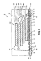
- FIG. 1 is a cross-sectional view showing an example of a semiconductor device of the present invention.
- FIG. 2 is a diagram for explaining a method of manufacturing the semiconductor device shown in FIG.
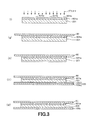
- FIG. 3 is a diagram for explaining a method of manufacturing the semiconductor device shown in FIG.
- FIG. 4 is a diagram for explaining a method of manufacturing the semiconductor device shown in FIG.
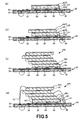
- FIG. 5 is a diagram for explaining a method of manufacturing the semiconductor device shown in FIG.
- FIG. 1 is a cross-sectional view showing an example of a semiconductor device of the present invention.
- a semiconductor device 10 shown in FIG. 1 is an example having a BGA (Ball Grid Array) type semiconductor package.
- the semiconductor device 10 includes a plurality of stacked semiconductor chips 20 (semiconductor elements), an adhesive layer 601 that bonds the semiconductor chips 20 to each other, a package substrate 30 that supports the semiconductor chips 20, a semiconductor chip 20 and a package substrate 30.
- An adhesive layer 101 for bonding the semiconductor chip 20, a mold part 50 for sealing the semiconductor chip 20, and a solder ball 80 provided below the package substrate 30.
- the configuration of each unit will be described in detail.
- the semiconductor chip 20 may be any kind of element, for example, a memory element such as a NAND (NotDRAMAND) flash memory, a DRAM (Dynamic ⁇ Random Access Memory), an IC (Integrated Circuit), or an LSI (Large Scale Integration). Such an integrated circuit element is mentioned.
- a memory element such as a NAND (NotDRAMAND) flash memory, a DRAM (Dynamic ⁇ Random Access Memory), an IC (Integrated Circuit), or an LSI (Large Scale Integration).
- a memory element such as a NAND (NotDRAMAND) flash memory, a DRAM (Dynamic ⁇ Random Access Memory), an IC (Integrated Circuit), or an LSI (Large Scale Integration).
- the constituent material of the semiconductor chip 20 is not particularly limited, and examples thereof include single crystal materials such as silicon, silicon carbide, and compound semiconductors, polycrystalline materials, and amorphous materials.
- the plurality of semiconductor chips 20 are stacked slightly shifted from each other in the in-plane direction, thereby forming a chip stack 200 (laminated semiconductor element).
- the semiconductor chips 20 are bonded to each other through an adhesive layer 601.
- the adhesive layer 601 is also provided on the upper surface of the chip stack 200.
- the adhesive layer 601 is composed of a cured product (photocured adhesive composition after curing) of the photosensitive adhesive composition of the present invention. The photosensitive adhesive composition will be described in detail later.
- a package substrate 30 shown in FIG. 1 is a build-up substrate including a core substrate 31, an insulating layer 32, a solder resist layer 33, wirings 34, and conductive vias 35.
- the core substrate 31 is a substrate that supports the package substrate 30 and is made of, for example, a composite material in which a glass cloth is filled with a resin material.
- the insulating layer 32 is an interlayer insulating layer that insulates the wirings 34 from each other and the wirings 34 and the conductive vias 35, and is made of, for example, a resin material.
- the solder resist layer 33 is a surface protective layer that protects the wiring formed on the outermost surface of the package substrate 30, and is made of, for example, a resin material.
- the wiring 34 and the conductive via 35 are each an electric signal transmission path, and are made of, for example, a metal material such as Au, Ag, Cu, Al, Ni alone or an alloy.
- the solder ball 80 is electrically connected to the wiring 34, and functions as an electrode for connecting the wiring 34 to another electric circuit by being fused to an external electric circuit.
- a chip stack 200 formed by stacking a plurality of semiconductor chips 20 is placed on the upper surface of the package substrate 30.
- the chip stack 200 and the package substrate 30 are bonded together by an adhesive layer 101.
- a part of the wiring 34 of the package substrate 30 is exposed on the upper surface of the package substrate 30 to constitute an exposed portion.
- the exposed portion and the electrode portion of each semiconductor chip 20 are connected by a bonding wire 70.
- Such a mold part 50 is comprised with various resin materials, such as an epoxy resin and a phenol resin, for example.
- FIGS. 2 to 5 are diagrams for explaining a method of manufacturing the semiconductor device shown in FIG.
- the upper part of FIGS. 2 to 5 is referred to as “upper” and the lower part is referred to as “lower”.
- the manufacturing method of the semiconductor device 10 includes a coating step of applying a liquid containing a photosensitive adhesive composition on a wafer (semiconductor substrate) to obtain a coating film, an exposure step of exposing the obtained coating film, and development.
- each process will be described sequentially.
- a wafer 201 (see FIG. 2A) for cutting out the semiconductor chip 20 is prepared, and a liquid containing the photosensitive adhesive composition is applied thereon (one surface side). Thereby, as shown in FIG. 2B, a coating film 601 a is formed on the wafer 201.
- a semiconductor circuit, an electrode pad, and the like are formed in advance corresponding to each semiconductor chip 20. That is, the wafer 201 is used for a so-called pre-process of the semiconductor manufacturing process. Therefore, a plurality of semiconductor chips 20 can be cut out from the wafer 201 by cutting the wafer 201 in steps described later and separating the wafer 201 into individual pieces.
- the coating method is not particularly limited, and examples thereof include a spin coating method, a spray coating method, an ink jet method, a roll coating method, and a printing method.
- a liquid (liquid film) containing the applied photosensitive adhesive composition may be heated and dried.
- the heating temperature is preferably 70 to 160 ° C., more preferably 80 to 150 ° C.
- the heating time is appropriately set according to the heating temperature, but is preferably 5 seconds to 30 minutes, and more preferably 10 seconds to 15 minutes.
- the liquid containing the photosensitive adhesive composition is prepared by appropriately adding a solvent or the like that can dissolve the liquid to the photosensitive adhesive composition of the present invention. Moreover, it is preferable that the solvent to be used can be removed by volatilization when heated in the process described later.
- solvents include toluene, xylene, benzene, dimethylformamide, tetrahydrofuran, ethyl cellosolve, ethyl acetate, N-methyl-2-pyrrolidone, ⁇ -butyrolactone, N, N-dimethylacetamide, dimethyl sulfoxide, diethylene glycol.
- a solvent containing any of propylene glycol monomethyl ether, propylene glycol monomethyl ether acetate, ⁇ -butyrolactone, and cyclohexanone is particularly preferable because of its high solubility and easy removal by volatilization.
- electromagnetic waves and particle beams having various wavelengths are used, and examples thereof include ultraviolet rays such as i-rays, visible rays, lasers, X-rays, and electron beams. Of these, ultraviolet rays or visible rays having a wavelength of about 200 to 700 ⁇ m are preferably used.
- the exposure process can be performed in, for example, an air atmosphere, an inert gas atmosphere, or a reduced pressure atmosphere.
- a mask provided apart from the coating film 601a may be used instead of the mask 4 provided in contact with the coating film 601a. Note that the use of a mask can be omitted when highly directional X-rays or electron beams are used for the exposure process.
- the exposure amount in the exposure process is appropriately set according to the thickness of the coating film 601a, the sensitivity of the photosensitive adhesive composition, and the like, but it is preferably about 30 to 3000 mJ / cm 2 as an example.
- the coating film 601a subjected to the exposure processing is subjected to development processing.
- the exposed portion is removed, and desired patterning is performed as shown in FIG.
- desired patterning for example, an electrode pad for connecting the bonding wire 70 to the semiconductor chip 20 can be exposed.
- the coating film 601a on the dicing line that is to be cut in the dicing process described later can be removed.
- a developer is brought into contact with the coating film 601a subjected to the exposure process. Thereby, the coating film 601a in the exposed portion is dissolved in the developer and removed. Thereby, the opening part 601b is formed in the coating film 601a.
- the developer include alkali metal carbonates, alkali metal hydroxides, alkali developers such as tetraammonium hydroxide, organic developers such as dimethylformamide and N-methyl-2-pyrrolidone, and the like. Can be mentioned.
- an alkaline developer is particularly preferably used as the developer. Note that the alkaline developer has a feature that a load on the environment is small and a residue is hardly generated.
- examples of the developer supply method include spraying, paddle, dipping, and ultrasonic methods.
- the coating film 601a has a so-called positive photosensitivity, but the coating film 601a may have a so-called negative photosensitivity.
- an etching process is performed on the wafer 201 provided with the coating film 601a.
- the coating film 601a including the opening 601b functions as an etching mask.
- an etching process is selectively performed on the surface (upper surface) of the wafer 201 in the region corresponding to the opening 601b.
- a passivation film is formed on the surface of the wafer 201, it can be removed and an electrode pad for connecting the bonding wire 70 can be exposed.
- Examples of the etching process include a plasma etching process (dry etching process) by supplying plasma to the wafer 201 and various wet etching processes as shown in FIG.
- the plasma etching process can be performed under generally known conditions.
- a fluorine compound gas CF 4 , CHF 3
- a fluorine compound gas CF 4 , CHF 3
- an oxygen gas O 2
- the output is 200 to 2000 W
- the time is 0.2 to 15 minutes
- the gas flow rate is 50 It can be performed under conditions of up to 1000 sccm.
- Examples of the ashing treatment include plasma treatment and wet treatment using a chemical.
- oxygen gas (O 2 ), a mixture gas of oxygen gas (O 2 ) and argon gas (Ar), or the like is used as the treatment gas, the output is 200 to 2000 W, and the treatment time is 0.2 to 15
- the gas flow rate can be set to 50 to 1000 sccm.
- a back grind film 90 is pasted on the coating film 601a.
- the back grind film 90 supports the wafer 201 during the back grind process, and suppresses occurrence of defects such as chipping and cracking in the wafer 201.
- the back surface (the other surface side) of the wafer 201 is ground (back grinding process). Thereby, the broken line portion in FIG. 3H is removed, and the thickness of the wafer 201 can be reduced.
- the thickness of the wafer 201 can be reduced to about 20 to 100 ⁇ m although it varies depending on the thickness of the original wafer 201.
- an apparatus called a back grinding wheel is used for the back grinding process.
- the adhesive layer 601 which expresses sufficient adhesive force between the semiconductor chips 20 can be cut out by cutting the coating film 601a obtained from the photosensitive adhesive composition of the present invention.
- the coating film 601a obtained from the photosensitive adhesive composition of the present invention also exhibits sufficient adhesive force to the back grind film 90. Therefore, by sticking the back grind film 90 on the coating film 601a, the back grind film 90 can reliably support the coating film 601a and the wafer 201. Thereby, since the position shift of the wafer 201 with respect to the back grind film 90 does not occur at the time of the back grind process, the highly accurate back grind process can be performed on the wafer 201. For this reason, the variation in the thickness of the wafer 201 can be suppressed. As a result, it is possible to obtain the semiconductor chip 20 in which inclination or the like hardly occurs when stacked.
- the coating film 601a is formed on the wafer 201 subjected to the back grinding process, and the back grinding process is performed in that state.
- the coating film 601a has mechanical characteristics that can reliably bond the semiconductor chips 20 to each other. Therefore, the coating film 601 a is interposed between the wafer 201 and the back grind film 90 and also has a function of mechanically supporting the wafer 201. Further, since the coating film 601a is slightly cured after being formed on the wafer 201 in a liquid phase state, the adhesion with the wafer 201 is good. Therefore, a more uniform process can be performed by performing the back grinding process on the wafer 201 provided with the coating film 601a.
- a UV peeling type back grind film can be used as the back grind film 90.
- the back grind film 90 is simply subjected to UV irradiation treatment through the back grind film 90.
- the adhesive force between 90 and the coating film 601a can be greatly reduced.
- the back grind film 90 can be smoothly peeled off from the coating film 601a without imposing a large burden on the coating film 601a.
- the dicing process is performed in a state where the wafer 201 is attached to a dicing die attach film or a dicing film.
- This dicing die attach film or dicing film is used for fixing the wafer 201 during the dicing process.
- FIGS. 3 (i1) and 3 (i2) are diagrams showing examples in which a dicing film 100a is attached to the back side of the wafer 201 ground in the back grinding process.
- FIG. 3I1 illustrates a wafer 201 and the like for cutting out the semiconductor chip 20 used for the lowermost layer (the layer closest to the package substrate 30) of the chip stack 200.
- FIG. 3 (i 2) illustrates a wafer 201 or the like for cutting out the semiconductor chip 20 used for a layer other than the lowermost layer of the chip stack 200.
- a dicing die attach film 100 which is a laminate of a dicing film 100a and a die attach film 100b, is attached to the back surface of the wafer 201.
- a dicing film 100 a is attached to the back surface of the wafer 201.
- the back grind film 90 is peeled from the coating film 601a.
- a dicing process is performed on the wafer 201 provided with the coating film 601a.
- the dicing process is performed so that the dicing blade 110 reaches the dicing film 100a as shown in FIGS. 4 (k1) and 4 (k2).
- the coating film 601a, the wafer 201, and the die attach film 100b are separated into individual pieces, and the adhesive layer 601, the semiconductor chip 20 (first semiconductor element), and the adhesive layer 101 are laminated as shown in FIG. 4 (k1).
- An individual piece 21 is cut out.
- the coating film 601a and the wafer 201 are separated into individual pieces, and as shown in FIG. 4 (k2), the individual piece 22 formed by laminating the adhesive layer 601 and the semiconductor chip 20 (second semiconductor element) is cut out. .
- a plurality of semiconductor chips 20 are cut out by performing a dicing process on one wafer 201 (a joined body of a plurality of semiconductor chips 20).
- the present invention is not limited to this, and for example, a plurality of semiconductor chips 20 that have been separated into pieces may be used.
- the dicing process can be omitted.
- the back grinding process can be omitted.
- the process order of the back grinding process and the dicing process is not limited to the order described above, and the order may be changed. That is, the back grinding process may be performed after the wafer 201 is subjected to the dicing process.
- FIG. 4 (L1) and FIG. 4 (L2) are diagrams illustrating an example in which the cut piece 21 and the piece 22 are picked up by the collet 121 of the bonding apparatus 120, respectively.
- the individual piece 21 is picked up by the collet 121 of the bonding apparatus 120 and is crimped (mounted) on the package substrate 30 as shown in FIG.
- the back surface of the semiconductor chip 20 and the package substrate 30 are bonded via the adhesive layer 101.
- the adhesive layer 101 is formed by separating the die attach film 100b.
- the adhesive layer 101 may be formed of, for example, an uncured product or a semi-cured product (photosensitive adhesive composition that has not been completely cured) of the photosensitive adhesive composition of the present invention.
- the package substrate 30 also corresponds to a non-joining member that is joined to the semiconductor element 20.
- the photosensitive adhesive composition of the present invention is used not only for bonding the semiconductor element 20 and the semiconductor element (bonded member) 20 but also for bonding the semiconductor element 20 and the package substrate (bonded member) 30. be able to.
- a to-be-joined member is not limited to these.
- the piece 22 is pressure-bonded onto the piece 21 previously mounted.
- two semiconductor chips 20 can be stacked via the adhesive layer 601.
- a chip stack 200 in which a large number of semiconductor chips 20 are stacked is obtained.
- the electrode portions of the semiconductor chip 20 can be exposed by laminating the semiconductor chips 20 while shifting the positions thereof.
- the adhesive layer 601 is heated. Thereby, the adhesive layer 601 exhibits a sufficient adhesive force, and the semiconductor chips 20 can be firmly bonded to each other.
- the heating temperature is preferably about 30 to 150 ° C.
- the crimping load at the time of mounting is about 0.1 to 100 N, and the crimping time is about 0.1 to 10 seconds.
- each semiconductor chip 20 and the exposed portion of the wiring 34 of the package substrate 30 are connected by a bonding wire 70 as shown in FIG.
- the semiconductor device 10 shown in FIG. 1 is obtained.
- the molding of the mold part 50 can be performed by, for example, using a transfer molding machine and injecting a sealing material into the mold.
- a transfer molding machine it is preferable that the temperature of the mold is about 130 to 250 ° C., the injection pressure is about 3 to 10 MPa, and the holding time after injection is about 10 seconds to 10 minutes.
- the molded part 50 and the adhesive layer 601 can be finally cured (completely cured) by heating the molded body as necessary.
- the heating temperature is preferably about 130 to 250 ° C.
- the heating time is preferably about 10 minutes to 10 hours.
- the manufacturing method of the semiconductor device of this invention may have a heating process between the said [3] image development process and a [4] processing process.
- this heating step the coating film 601a subjected to the development process is heated (see FIG. 2 (e)).
- a predetermined curing reaction thermalsetting reaction
- the photosensitive adhesive composition is slightly cured (semi-cured), and the adhesiveness of the coating film 601a is increased.
- the heating temperature of the coating film 601a is not particularly limited, but is preferably 80 to 170 ° C, and more preferably 120 to 160 ° C.
- the heating time is appropriately set according to the heating temperature, but is preferably 35 to 120 minutes, and more preferably 40 to 100 minutes. Thereby, mechanical properties such as the elastic modulus of the coating film 601a are optimized, and sufficient resistance to the etching process and the ashing process is imparted to the coating film 601a.
- the coating film 601a is formed of the photosensitive adhesive composition of the present invention, and the adhesive layer 601 formed from such a coating film 601a exhibits a relatively high solubility in an organic solvent. For this reason, for example, even when it is necessary to remove the coating film 601a after forming the coating film 601a on the wafer 201, the coating film 601a is efficiently dissolved while suppressing the generation of residues (residues). Can be removed. For this reason, the wafer 201 can be used again (reworked) without being wasted. As a result, the process yield of the semiconductor device 10 can be improved.
- the manufacturing method of the semiconductor device may include a step of irradiating light on the entire surface of the coating film (light irradiation step) in addition to the heating step or instead of the heating step.
- the photosensitive adhesive composition contains (A) an alkali-soluble resin, (B) a photoacid generator, (C) an epoxy compound, and (D) a phenol compound.
- the alkali-soluble resin is a material that becomes a base material of the adhesive layer 601.
- the photosensitive adhesive composition can enhance the adhesive force (adhesive force) of the adhesive layer 601 to the semiconductor chip 20 by including (A) an alkali-soluble resin. Therefore, the semiconductor chips 20 can be more firmly bonded to each other depending on the adhesive layer 601.
- the photosensitive adhesive composition contains (A) an alkali-soluble resin, the coating film 601a can be provided with solubility in an alkali developer. For this reason, an alkaline developer having a small environmental load can be used, and the environmental load in the development process can be reduced.
- the alkali-soluble resin examples include phenolic resins, acrylic resins, cyclic olefin resins, polyamide resins, polyimide resins, polyvinylphenol resins, etc. Species or a combination of two or more can be used. Among these, (A) the alkali-soluble resin is particularly preferably a cyclic olefin resin.
- cyclic olefin resins include norbornene resins and benzocyclobutene resins. Among these, as the cyclic olefin resin, a norbornene resin is preferable.
- an adhesive layer 601 that is particularly excellent in adhesive strength to the semiconductor chip 20 can be obtained.
- the adhesive force of the adhesive layer 601 to the semiconductor chip 20 can be further increased by using a photosensitive adhesive composition containing a norbornene-based resin.
- norbornene-type resin has high hydrophobicity, the adhesive layer 601 which cannot produce the dimensional change by water absorption etc. easily can be formed by using the photosensitive adhesive composition containing norbornene-type resin.
- the alkali-soluble resin is a cyclic olefin resin
- cyclic olefin resin has an acidic group (substituent which shows acidity).
- the cyclic olefin resin preferably has at least one repeating unit having an acidic group (first repeating unit).
- the first repeating unit has a structure derived from a cyclic olefin (cyclic olefin monomer) as a main skeleton and a substituent having an acidic group bonded to this structure.
- cyclic olefins monocyclic compounds such as cyclohexene and cyclooctene, norbornene, norbornadiene, dicyclopentadiene, dihydrodicyclopentadiene, tetracyclododecene, tricyclopentadiene, dihydrotricyclopentadiene, tetracyclopentadiene, Examples include structures derived from polycyclic compounds such as dihydrotetracyclopentadiene. Among these, the structure derived from a cyclic olefin is particularly preferably a structure derived from norbornene.
- the structure derived from norbornene contributes to an improvement in the adhesive force of the adhesive layer 601 to the semiconductor chip 20. Moreover, the structure derived from norbornene also contributes to the improvement of the heat resistance of the photosensitive adhesive composition and the flexibility of the photosensitive adhesive composition after curing.
- substituent having an acidic group examples include a substituent having a carboxyl group, a phenolic hydroxyl group, —C (OH) — (CF 3 ) 2 , —N (H) —S (O) 2 —CF 3, and the like.
- a substituent having either a carboxyl group or —C (OH) — (CF 3 ) 2 is particularly preferable.
- cyclic olefin resin contains the substituent which has such an acidic group, the solubility with respect to the alkaline developing solution of the photosensitive adhesive composition can be improved. Therefore, in the manufacture of a semiconductor device, the undissolved residue of the photosensitive adhesive composition after development can be reduced, and the patterning property during development can be further improved.
- the first repeating unit is particularly preferably at least one of the following formula (2) and the following formula (3).
- the cyclic olefin-based resin contains such a first repeating unit, the adhesiveness of the adhesive layer 601 to the semiconductor chip 20 and the solubility of the photosensitive adhesive composition in an alkaline developer can be further improved.
- x and y are each preferably an integer of 0 or more and 10 or less, and more preferably an integer of 1 or more and 5 or less.
- the cyclic olefin-based resin only needs to have at least one first repeating unit, but preferably has two or more different first repeating units, and the above-mentioned formulas (2) and (3) It is more preferable to have both first repeating units. Thereby, the adhesiveness with respect to the semiconductor chip 20 of the contact bonding layer 601 and the solubility with respect to the alkaline developing solution of a photosensitive adhesive composition can further be improved.
- the content of the first repeating unit in the cyclic olefin-based resin can be determined optimally in consideration of the solubility of the photosensitive adhesive composition in an alkaline developer, and is, for example, 10 to 80 mol%. It is preferable that it is 20 to 70 mol%. If the content of the first repeating unit is less than the lower limit, it may be difficult to sufficiently develop the solubility of the photosensitive adhesive composition in an alkaline developer. Moreover, when the content rate of a 1st repeating unit exceeds the said upper limit, depending on the kind of 1st repeating unit, the characteristic with which structures other than the 1st repeating unit of cyclic olefin resin are equipped is fully expressed. It may not be possible.
- the acidic group in the cyclic olefin resin is preferably 0.001 to 0.01 mol per 1 g of the polymer.
- the amount is more preferably 0.0015 to 0.006 mol.
- the cyclic olefin-based resin also has a second repeating unit different from the first repeating unit described above.
- the second repeating unit includes a structure derived from a cyclic olefin as a main skeleton and a substituent that is bonded to the structure and is different from the substituent of the first repeating unit.
- the main skeleton of the second repeating unit As the main skeleton of the second repeating unit, the structure exemplified in the first repeating unit described above can be used.
- the main skeleton of the second repeating unit is a structure derived from norbornene from the viewpoint of heat resistance of the photosensitive adhesive composition and flexibility of the photosensitive adhesive composition after curing. Is particularly preferred.
- the main skeletons of the first and second repeating units may be different from each other, but are preferably the same.
- the main skeletons of the first and second repeating units are preferably structures derived from norbornene.
- the semiconductor chip 20 of the contact bonding layer 601 can be more firmly bonded to each other by the adhesive layer 601, and the stress concentration generated at the bonding interface between the semiconductor chips 20 can be reduced by appropriately increasing the flexibility of the adhesive layer 601. Can do.
- the substituent of the second repeating unit preferably has 2 to 30 carbon atoms, and more preferably 4 to 15 carbon atoms.
- the carbon number is within the above range, the elastic modulus of the cured photosensitive adhesive composition is lowered, and the flexibility of the adhesive layer 601 can be increased. Thereby, the crack which arises in the semiconductor chip 20 and the contact bonding layer 601 accompanying the stress concentration in the joining interface of the semiconductor chips 20 and peeling with the semiconductor chip 20 and the contact bonding layer 601 can further be suppressed. In addition, it is possible to suppress the occurrence of damage to the semiconductor chip 20 and the adhesive layer 601 due to external impact.
- the substituent of the second repeating unit may be a cyclic structure, a branched structure, or the like, but is preferably a linear structure.
- linear substituent having 2 to 30 carbon atoms examples include an alkyl group, an alkenyl group, an alkynyl group, an aryl group, an aralkyl group, and a group having an alkyl ether structure.
- the linear substituent having 2 to 30 carbon atoms is particularly preferably a group having an alkyl ether structure.
- the group having an alkyl ether structure is particularly preferably a group represented by the following formula (1). Thereby, the softness
- z is preferably an integer of 1 or more and 10 or less, and more preferably an integer of 2 or more and 6 or less.
- the second repeating unit is particularly preferably the following formula (4).
- the alkali-soluble resin has a second repeating unit represented by the following formula (4), whereby a photosensitive adhesive composition for an alkaline developer by the first repeating unit.
- the function of sufficiently increasing the solubility of the product and the function of setting the elastic modulus of the photosensitive adhesive composition after curing by the second repeating unit to an appropriate value can be preferably achieved.
- z is preferably an integer of 1 to 10, more preferably an integer of 2 to 5.
- the content of the second repeating unit in the cyclic olefin-based resin is preferably, for example, 20 to 60 mol%, and preferably 25 to 50 mol%. Is more preferable.
- the content rate of the second repeating unit is less than the lower limit, it is difficult to adjust the elastic modulus of the photosensitive adhesive composition after curing to a desired value depending on the type of the second repeating unit. There is a case.
- the content rate of a 2nd repeating unit exceeds the said upper limit, depending on the kind of 2nd repeating unit, the characteristic with which structures other than a 2nd repeating unit of cyclic olefin resin are equipped fully is expressed. It may not be possible.
- a cyclic olefin resin represented by the following formula (5) is preferably used.
- the photosensitive adhesive composition imparts mechanical strength necessary for the adhesive layer 601 and more appropriate flexibility (stress relaxation). be able to.
- the photosensitive adhesive composition can exhibit particularly excellent solubility in an alkali developer.
- l, m, and n are integers of 1 to 100.
- x is preferably an integer of 0 or more and 10 or less
- y is preferably an integer of 0 or more and 10 or less
- z is an integer of 1 or more and 10 or less. preferable.
- the degree of polymerization of the second repeating unit relative to the degree of polymerization of the first repeating unit is preferably 0.3 to 2.0, 0 More preferably, it is 4 to 1.5.
- the weight average molecular weight (Mw) of the cyclic olefin resin is preferably 5,000 to 500,000, more preferably 7,000 to 200,000, and 8,000 to 100,000. Is more preferable. Thereby, it is possible to obtain the adhesive layer 601 that is particularly excellent in the adhesive force to the semiconductor chip 20.
- the weight average molecular weight (Mw) of the cyclic olefin resin can be measured by gel permeation chromatography (GPC) using a standard cyclic olefin resin according to ASTM D3536-91. .
- the glass transition temperature of the cyclic olefin resin is preferably 100 to 250 ° C.
- the glass transition temperature of the cyclic olefin-based resin can be determined as a temperature at which an exothermic reaction occurs when the temperature is raised from room temperature at a rate of temperature rise of 5 ° C./min, for example, by differential scanning calorimetry.
- the (A) alkali-soluble resin other than the cyclic olefin resin is also synthesized so as to satisfy the same conditions as described for the cyclic olefin resin, thereby obtaining the same effect as described above.
- the photo acid generator is a positive type light that can generate acid by photoreaction during exposure by energy beam irradiation and increase the solubility of the photosensitive adhesive composition in the alkali developer in the exposed area. It functions as an acid generator. Thereby, in manufacture of a semiconductor device, it can further reduce that the melt
- the photosensitive adhesive composition contains (B) a photoacid generator, so that, in the manufacture of a semiconductor device, (C) a reaction that crosslinks (A) an alkali-soluble resin with an epoxy compound described later by irradiation with energy rays. It may have a function as a negative photoacid generator capable of promoting the above.
- (B) photoacid generators include onium salts, halogenated organic compounds, quinonediazide compounds, ⁇ , ⁇ -bis (sulfonyl) diazomethane compounds, ⁇ -carbonyl- ⁇ -sulfonyl-diazomethane compounds. , Sulfone compounds, organic acid ester compounds, organic acid amide compounds, organic acid imide compounds, and the like, and one or more of these can be used in combination.
- a quinonediazide compound examples include compounds having a 1,2-benzoquinonediazide or 1,2-naphthoquinonediazide structure.
- the photoacid generator is an ester of 1,2-naphthoquinone-2-diazide-5-sulfonic acid or 1,2-naphthoquinone-2-diazide-4-sulfonic acid and a phenol compound. It is preferable to include a compound. Since these generate a carboxyl group by a photoreaction at the time of exposure by energy ray irradiation (particularly, radiation irradiation), it is possible to further increase the solubility of an exposed portion in an alkaline developer. For this reason, the photosensitive adhesive composition can exhibit higher solubility in an alkali developer even at a small exposure amount. As a result, the patterning property during development can be further improved.
- the content of the (B) photoacid generator is not particularly limited, but it is preferably 1 to 50 parts by mass, more preferably 5 to 30 parts by mass with respect to 100 parts by mass of the (A) alkali-soluble resin. preferable.
- the content of the photoacid generator is less than the lower limit, depending on the type of the (B) photoacid generator, the exposure and development characteristics of the photosensitive adhesive composition may be deteriorated. . Further, even if the content of (B) the photoacid generator exceeds the above upper limit, no further increase in effect can be expected, and depending on the type of (B) photoacid generator, in the photosensitive adhesive composition In (B), the characteristics of materials other than the photoacid generator may not be sufficiently exhibited.
- Epoxy compound has a function which bridge
- alkali-soluble resin especially cyclic olefin resin.
- the epoxy compound may be either an aromatic epoxy compound having an aromatic ring in the molecule or an aliphatic epoxy compound having no aromatic ring in the molecule.
- the (C) epoxy compound is more preferably an aliphatic epoxy compound.
- the (C) epoxy compound preferably has a branched structure or a linear structure, and more preferably has a branched structure.
- the crosslinking density of the (A) alkali-soluble resin in the photosensitive adhesive composition can be set to an appropriate value.
- the flexibility of the adhesive layer 601 can be increased moderately. As a result, an adhesive layer 601 that has the necessary mechanical strength and is superior in stress relaxation property that relieves stress concentration generated at the bonding interface between the semiconductor chips 20 can be obtained.
- the (C) epoxy compound preferably contains two or more glycidyl groups in the molecule, and more preferably contains 3 or more and 9 or less glycidyl groups in the molecule.
- the crosslink density of the (A) alkali-soluble resin in the photosensitive adhesive composition can be set to an appropriate value, and an adhesive layer 601 that has the necessary mechanical strength and is excellent in stress relaxation properties can be obtained. Can do.
- Examples of such (C) epoxy compounds include ethylene glycol diglycidyl ether, propylene glycol diglycidyl ether, polyethylene glycol diglycidyl ether, polypropylene glycol diglycidyl ether, trimethylolpropane triglycidyl ether, trimethylolethane triglycidyl ether.
- (C) epoxy compounds include trimethylolpropane triglycidyl ether, 1,6-hexanediol diglycidyl ether, polypropylene glycol diglycidyl ether, polyethylene glycol diglycidyl ether, polytetramethylene glycol diglycidyl ether, hydrogenated Bisphenol A diglycidyl ether is particularly preferred.
- the crosslinking reaction of the (A) alkali-soluble resin in the photosensitive adhesive composition can be promoted, and the adhesive layer 601 superior in stress relaxation can be obtained more easily and more reliably.
- the content of the epoxy compound is not particularly limited, but it is preferably 1 to 100 parts by mass, more preferably 5 to 50 parts by mass with respect to 100 parts by mass of (A) the alkali-soluble resin.
- the content of the (C) epoxy compound is less than the lower limit, the stress relaxation property of the adhesive layer 601 may be lowered depending on the type of the (C) epoxy compound.
- the content of the epoxy compound (C) exceeds the upper limit, the viscosity of the photosensitive adhesive composition may be unnecessarily high.
- the photosensitive adhesive composition includes, for example, a coating film 601a by including (D) a phenol compound having a melting point of 50 to 150 ° C. (hereinafter, also simply referred to as “(D) phenol compound”). It is possible to suppress the generation of bubbles between the adhesive layer 601 and the semiconductor chip 20 when the wafer 201 is etched or when the semiconductor chips 20 are pressure-bonded via the adhesive layer 601. Further, even when bubbles are generated between the adhesive layer 601 and the semiconductor chip 20, the generated bubbles can be removed.
- the adhesive force of the adhesive layer 601 to the semiconductor chip 20 can be increased, and thus the semiconductor chips 20 are firmly bonded to each other. be able to. Therefore, finally, a highly reliable chip stack 200 can be obtained.
- an adhesive layer 601 showing relatively high solubility in an organic solvent can be obtained. For this reason, for example, even when it becomes necessary to remove the coating film 601a obtained by applying the photosensitive adhesive composition to the wafer 201, the coating film 601a is made efficient while suppressing the generation of residues (residues). It can be dissolved and removed well. Thereby, the wafer 201 can be used again (reworked) without wasting it. Therefore, the process yield of the semiconductor device 10 can be improved.
- the (D) phenol compound has a melting point of 50 to 150 ° C., preferably a melting point of 60 to 130 ° C., more preferably 70 to 120 ° C. Thereby, the effect mentioned above by the photosensitive adhesive composition containing (D) phenolic compound can be exhibited more notably.
- Such (D) phenol compound preferably contains at least one of a phenol compound having a substituent containing an aliphatic hydrocarbon group and a phenol compound having a plurality of phenol skeletons.
- the (D) phenol compound (particularly a phenol compound having a substituent containing an aliphatic hydrocarbon group) preferably has a hydroxyl group equivalent of 150 to 250 g / eq, and a hydroxyl group equivalent of 160 to 240 g / eq. More preferably, the hydroxyl equivalent is 180 to 220 g / eq.
- the hydroxyl equivalent is within the above range, a photosensitive adhesive composition having more optimal solubility in an alkali developer can be obtained.
- the hydroxyl group equivalent is less than the lower limit, depending on the type and amount of the (D) phenol compound, the water absorption rate of the photosensitive adhesive composition is increased, and the reliability may be reduced. There is sex.
- the hydroxyl equivalent exceeds the upper limit, the solubility of the photosensitive adhesive composition in an alkaline developer is remarkably lowered, and the photosensitive adhesive composition may remain undissolved after development.
- the hydroxyl equivalent of (D) phenolic compound can be measured by a method of titrating a solution obtained by mixing (D) phenolic compound in standard alkaline solution.
- the adhesive layer 601 has more solubility in an organic solvent. Can be increased. For this reason, even when it is necessary to remove the coating film 601a, the coating film 601a can be dissolved and removed more efficiently, so that the reworkability can be improved.
- n is preferably 1 to 6, and more preferably 2 to 4.
- Examples of such a substituent containing an aliphatic hydrocarbon group include a methylene group, an ethylene group, a trimethylene group, a butyl group, and a 2,2-dimethylbutyl group.
- the phenol compound preferably has a structure derived from benzoic acid. Specifically, it preferably has a structure derived from monohydroxybenzoic acid such as benzoic acid, 2-hydroxybenzoic acid and 3-hydroxybenzoic acid, and dihydroxybenzoic acid such as 2,4-hydroxybenzoic acid.
- phenolic compounds include 4- (1,1-dimethylpropyl) phenol, 4-cyclohexylphenol, 4- (1,1,3,3-tetramethylbutyl).
- the hydroxyl equivalent is preferably 50 to 150 g / eq, more preferably 70 to 130 g / eq, and more preferably 90 to Particularly preferred is 110 g / eq.
- multiple phenol skeletons are linked polycyclic structures in which the phenol skeletons are linked by single bonds and are not directly bonded to each other, or condensed types in which the phenol skeletons are directly bonded to each other without a single bond (fusion) Type) polycyclic structures may be used, but a linked polycyclic structure is preferred.
- an adhesive layer 601 that has particularly high adhesion to the semiconductor chip 20 and is more soluble in organic solvents.
- the content of the phenolic compound is preferably 0.5 to 30 parts by mass and more preferably 1 to 20 parts by mass with respect to 100 parts by mass of the (A) alkali-soluble resin. If the content of the (D) phenol compound is less than the lower limit, the solubility of the photosensitive adhesive composition in the organic solvent may be reduced depending on the type of the (D) phenol compound. (D) Even if content of a phenol compound exceeds the said upper limit, the increase of the effect beyond it cannot be anticipated. In this case, depending on the type of the (D) phenol compound, the characteristics of materials other than the (D) phenol compound in the photosensitive adhesive composition may not be sufficiently exhibited.
- the photosensitive adhesive composition contains two or more (D) phenol compounds as described above. Specifically, it is preferable to include two or more types of (D) phenol compounds having different melting points, and more preferably to include two types of (D) phenol compounds having different melting points. Thereby, the adhesiveness of the photosensitive adhesive composition (adhesive layer 601), stress relaxation property, and the solubility with respect to the organic solvent can be improved more.
- the photosensitive adhesive composition contains (A) an alkali-soluble resin, (B) a photoacid generator, (C) an epoxy compound, and (D) a phenol compound as described above, thereby manufacturing a semiconductor device.
- A an alkali-soluble resin
- B a photoacid generator
- C an epoxy compound
- D a phenol compound as described above
- Such a semiconductor device 10 has a very small internal volume, such as a mobile device, and is particularly useful in an electronic device that is used while being carried. That is, such a semiconductor device 10 is useful in that it contributes to the reduction in size, thickness, and weight of the electronic device and that the function of the semiconductor device 10 is hardly impaired even when the electronic device is dropped or swung. It is.
- the cured product of the photosensitive adhesive composition containing (A) an alkali-soluble resin, (B) a photoacid generator, (C) an epoxy compound, and (D) a phenol compound is soluble in an organic solvent. Excellent reworkability.
- such a photosensitive adhesive composition further includes (X) a phenol compound having a higher melting point than (D) the phenol compound.
- the melting point of the (X) phenol compound is preferably 151 to 250 ° C, and more preferably 181 to 230 ° C.
- the (X) phenol compound preferably includes a phenol compound having a plurality of phenol skeletons.
- Such a phenol compound having a plurality of phenol skeletons preferably has a substituent containing a cyclic structure and has at least one substituent bonded to the phenol skeleton. Thereby, the said effect can be exhibited more notably.
- the content of the (X) phenol compound is preferably 0.2 to 20 parts by mass, more preferably 0.5 to 10 parts by mass with respect to 100 parts by mass of the (A) alkali-soluble resin. . (X) When content of a phenol compound exists in the said range, the effect mentioned above can be exhibited more notably.
- the photosensitive adhesive composition contains (D) two types of phenolic compounds and further contains (X) a phenolic compound. Thereby, it is possible to obtain an adhesive layer 601 that is particularly excellent in adhesiveness, stress relaxation, and solubility in an organic solvent.
- the photosensitive adhesive composition may contain (D) a phenol compound and (X) a phenol compound other than the phenol compound, a leveling agent, a flame retardant, a plasticizer, a curing accelerator, an antioxidant, an adhesion assistant, if necessary.
- An agent or the like may be further included.
- the antioxidant examples include a phenolic antioxidant, an amine antioxidant, a phosphorus antioxidant, and a thioether antioxidant, and one or a combination of two or more of these may be used. it can. However, among these, it is preferable to use a combination of a phenolic antioxidant and an amine antioxidant as the antioxidant.
- phenolic antioxidants include pentaerythrityl-tetrakis [3- (3,5-di-t-butyl-4-hydroxyphenyl) propionate], 3,9-bis ⁇ 2- [3- (3-t -Butyl-4-hydroxy-5-methylphenyl) propionyloxy] -1,1-dimethylethyl ⁇ 2,4,8,10-tetraoxaspiro [5,5] undecane, octadecyl-3- (3,5- Di-t-butyl-4-hydroxyphenyl) propionate, 1,6-hexanediol-bis [3- (3,5-di-t-butyl-4-hydroxyphenyl) propionate], 1,3,5-trimethyl -2,4,6-tris (3,5-di-t-butyl-4-hydroxybenzyl) benzene, 2,6-di-t-butyl-4-methylphenol, 2,6-di t-butyl-4-
- amine antioxidants include N, N′-di-sec-butyl-p-phenylenediamine, 4,4′-dimethoxydiphenylamine, 4-isopoloxydiphenylamine, and N-isopropyl-N′-phenyl-p-phenylene.
- examples thereof include diamine, N- (1,3-dimethylbutyl) -N′-phenyl-p-phenylenediamine, and 4,4′-di ( ⁇ , ⁇ -dimethylbenzyl) diphenylamine.
- the amine antioxidant is preferably a diphenylamine compound such as 4,4'-dimethoxydiphenylamine, 4-isopoloxydiphenylamine, or 4,4'-di ( ⁇ , ⁇ -dimethylbenzyl) diphenylamine.
- Phosphorus antioxidants include bis- (2,6-di-t-butyl-4-methylphenyl) pentapentaerythritol diphosphite, tris (2,4-di-t-butylphenylphosphite), tetrakis (2,4-di-t-butyl-5-methylphenyl) -4,4′-biphenylenediphosphonite, 3,5-di-t-butyl-4-hydroxybenzylphosphonate-diethyl ester, bis- (2,6 -Dicumylphenyl) pentaerythritol diphosphite, 2,2-methylenebis (4,6-di-t-butylphenyl) octyl phosphite, Tris (mixed mono and di-nonylphenyl phosphite), bis (2, 4-di-t-butylphenyl) pentapentaerythritol-di-
- Thioether antioxidants include dilauryl 3,3′-thiodipropionate, bis (2-methyl-4- (3-n-dodecyl) thiopropionyloxy) -5-t-butylphenyl) sulfide, distearyl- 3,3′-thiodipropionate, pentaerythritol-tetrakis (3-lauryl) thiopropionate, and the like.
- the content of the antioxidant is preferably 0.1 to 50 parts by mass with respect to 100 parts by mass of the (A) alkali-soluble resin, 0.5 More preferred is 30 parts by mass.
- adhesion assistants include vinyltrimethoxysilane, vinyltriethoxysilane, 3-glycidoxypropyltrimethoxysilane, 3-glycidoxypropylmethyldiethoxysilane, 3-glycidoxypropyltriethoxysilane, 5 , 6-epoxyhexyltriethoxysilane, p-styryltrimethoxysilane, 3-methacryloxypropylmethyldimethoxysilane, 3-methacryloxypropyltrimethoxysilane, 3-methacryloxypropylmethyldiethoxysilane, 3-methacryloxypropyltri Ethoxysilane, 3-acryloxypropyltrimethoxysilane, bis [3- (triethoxysilyl) propyl] tetrasulfide, bis [3- (triethoxysilyl) propyl] disulfide, 3-isocyanate propi Triethoxysilane, phenyltri
- the adhesion assistant is not limited to these. These may be used alone or in admixture of two or more. By including such an adhesion assistant in the photosensitive adhesive composition, the adhesive force (adhesion force) of the adhesive layer 601 to the semiconductor chip 20 can be further increased.
- the content of the adhesion assistant is preferably 0.1 to 30 parts by mass with respect to 100 parts by mass of the (A) alkali-soluble resin, 0.2 More preferred is 20 parts by mass.
- the elastic modulus at 25 ° C. of the photosensitive adhesive composition after curing is preferably 2.0 to 3.5 GPa.
- the elastic modulus at 25 ° C. of the photosensitive adhesive composition before curing is preferably 70 to 120% of the elastic modulus at 25 ° C. of the photosensitive adhesive composition after curing.
- the adhesive strength of the photosensitive adhesive composition before being subjected to etching treatment and ashing treatment to the semiconductor chip 20 at 25 ° C. is preferably 20.0 to 200.0 N.
- a film is formed on the semiconductor chip 20 having a size of 4 mm ⁇ 4 mm in plan view, and the film is not cured (completely cured) without being cured or semi-cured.
- the adhesion strength of the film to the semiconductor chip 20 at 25 ° C. is 20.0 to 200.0 N It is preferable that When this adhesive force is converted per unit area of the size of the semiconductor chip 20 in plan view, it is 1.25 to 12.5 MPa (N / mm 2 ).
- the elastic modulus at 25 ° C. of the photosensitive adhesive composition before curing is within a predetermined range with respect to the elastic modulus at 25 ° C. of the photosensitive adhesive composition after curing, for example, curing
- the risk of the previous photosensitive adhesive composition being significantly deformed or flowing out of the wafer 201 is reduced. For this reason, it is possible to improve the alignment accuracy when the semiconductor chips 20 are stacked.
- the amount of change in elastic modulus before and after curing is relatively small, the amount of shrinkage associated with exposure can also be reduced. As a result, it is possible to reduce stress generated at the interface between the adhesive layer 601 and the semiconductor chip 20 along with curing shrinkage. From this viewpoint, it contributes to improving the reliability of the chip stack 200.
- the pre-curing photosensitive adhesive composition that has been subjected to the etching process and the ashing process has sufficient adhesion to the semiconductor chip 20 required for die bonding.
- the adhesive layer 601 more firmly fixes the semiconductor chips 20 to each other and contributes to improving the reliability of the chip stack 200.
- the adhesive layer 601 combines the element protection function (buffer coating function) of the buffer coating film and the bonding function (die bonding function) of the die bonding film with one layer. For this reason, it is possible to form the chip stacked body 200 without reducing the reliability of the chip stacked body 200, and it is possible to make the chip stacked body 200 thinner than the conventional case where two layers are used. Further, as the chip stack 200 is made thinner, the volume of the mold part 50 can be reduced and the bonding wire 70 can be shortened, thereby contributing to weight reduction and cost reduction.
- the elastic modulus at 25 ° C. of the cured photosensitive adhesive composition is more preferably 2.2 to 3.2 GPa, and further preferably 2.4 to 3.0 GPa.
- the elasticity modulus of the photosensitive adhesive composition after hardening is less than the said lower limit, there exists a possibility that the adhesive force of the contact bonding layer 601 may fall a little depending on the composition of the photosensitive adhesive composition.
- the filler may penetrate the adhesive layer 601 and adversely affect the semiconductor chip 20.
- the elastic modulus of the cured photosensitive adhesive composition exceeds the upper limit, depending on the composition of the photosensitive adhesive composition, the flexibility of the adhesive layer 601 is reduced, so that the stress relaxation property is reduced. .
- the residual stress caused by the stacking of the semiconductor chips 20 and the local concentration of the thermal stress due to the thermal expansion difference between the semiconductor chip 20 and the adhesive layer 601 cannot be reduced, and the semiconductor chip 20 is cracked. May cause it.
- the elastic modulus of the cured photosensitive adhesive composition is, for example, using an ultra-micro hardness meter ENT-1000 (manufactured by Elionix Co., Ltd.), measuring temperature 25 ° C., load 2 mN, holding time 1 second, It can be determined by measuring in accordance with ISO14577 using a Berkovich indenter (triangular pyramid, opposite ridge angle 115 °).
- the elastic modulus of the cured photosensitive adhesive composition can be obtained as the elastic modulus of the coating film 601a after the mounting process.
- the elastic modulus at 25 ° C. of the photosensitive adhesive composition before curing is more preferably 75 to 115% with respect to the elastic modulus at 25 ° C. of the photosensitive adhesive composition after curing. More preferably, it is 80 to 110%.
- the elasticity modulus of the photosensitive adhesive composition before hardening is less than the said lower limit, the adhesiveness of the photosensitive adhesive composition increases, but the film of the photosensitive adhesive composition is easily deformed. As a result, for example, when the semiconductor chip 20 is temporarily arranged through this film, the position may be easily shifted, or the photosensitive adhesive composition may flow out of the wafer 201.
- the elastic modulus of the photosensitive adhesive composition before curing exceeds the upper limit value, the tackiness is lowered, and it may be difficult to temporarily arrange the semiconductor chip 20.
- the elasticity modulus of the photosensitive adhesive composition before hardening can also be measured similarly to the elasticity modulus of the photosensitive adhesive composition after hardening.
- the elastic modulus of the photosensitive adhesive composition before curing can be obtained as the elastic modulus of the coating film 601a after the processing step and before the mounting step.
- the adhesive strength at 25 ° C. of the photosensitive adhesive composition before being subjected to the etching treatment and the ashing treatment to the semiconductor chip 20 is more preferably 30 to 180 N (1.875 to 11.25 MPa). More preferably, the pressure is 40 to 160 N (2.5 to 10 MPa). Note that when the adhesive force is lower than the lower limit, bubbles may easily enter the interface between the adhesive layer 601 and the semiconductor chip 20. On the other hand, if the adhesive force exceeds the upper limit, if bubbles enter the interface between the adhesive layer 601 and the semiconductor chip 20, it may be difficult to remove.
- the adhesive force with respect to the semiconductor chip 20 of the photosensitive adhesive composition before being subjected to the etching treatment and the ashing treatment can be measured as follows. First, the semiconductor chips 20 are bonded to each other through the photosensitive adhesive composition of the present invention before being subjected to etching treatment and ashing treatment to obtain a semiconductor chip bonded body. Thereafter, the universal bond tester Dage4000 (manufactured by Daisy Japan Co., Ltd.) is used to determine the die shear strength of the bonded semiconductor chip as the adhesive strength to the semiconductor chip 20.
- the die shear strength is obtained when one semiconductor chip 20 is pushed in the horizontal direction (in-plane direction of the semiconductor chip 20) with a shear tool from the side (side surface) of the semiconductor chip bonded body, and the joint surface between the semiconductor chips 20 is broken. Required as strength.
- the adhesive force with respect to the semiconductor chip 20 of the photosensitive adhesive composition before being subjected to the etching process and the ashing process is obtained as an adhesive force with respect to the semiconductor chip 20 of the coating film 601a after the processing step and before the mounting step. be able to.
- the said etching process is a process which removes the passivation film on the surface of the semiconductor chip 20, and exposes the electrode pad for connecting the bonding wire 70, for example.
- a mixed gas of fluorine compound gas (CF 4 ), argon gas (Ar), and oxygen gas (O 2 ) is used as the gas, the output is 2500 W, the time is 6 minutes, and the CF 4 flow rate / Ar flow rate / O.
- the etching process performed on the conditions which 2 flow volume is 200 sccm / 200 sccm / 50 sccm is mentioned.
- the ashing process is a process for removing, for example, processing residues generated by the etching process and cleaning the surface of the adhesive layer 601 and the electrode pad surface.
- plasma treatment is performed using oxygen gas (O 2 ), an output of 600 W, a time of 12 minutes, and an O 2 flow rate of 200 sccm.
- etching treatment and ashing treatment may promote deterioration of the organic material. For this reason, when it is a coating film (adhesion layer) with low etching resistance and ashing resistance, there exists a possibility that the semiconductor chips 20 cannot fully be adhere
- the coating film 601a (adhesive layer 601) formed using the photosensitive adhesive composition has sufficient etching resistance and ashing resistance. For this reason, even after passing through such etching treatment and ashing treatment, a decrease in the adhesive strength of the coating film 601a is suppressed, and as a result, the adhesive strength as described above is exhibited. Therefore, such a photosensitive adhesive composition does not need to consider a decrease in adhesiveness in various treatments in the bonding process, and thus simplifies the manufacturing process and the cost reduction of the semiconductor device 10. It is useful in that it can.
- the rate of change of the elastic modulus of the photosensitive adhesive composition before and after the treatment step is preferably within a certain range. Therefore, it is preferable to appropriately set the heating conditions in the heating step that is considered to affect the resistance to the processing step (etching resistance and ashing resistance) so that the rate of change is within a certain range.
- the elastic modulus at 25 ° C. after the heating step and before the processing step of the photosensitive adhesive composition is X [GPa]
- the elastic modulus at 25 ° C. after the processing step is Y [GPa].
- X and Y preferably satisfy the relationship of 0.7 ⁇ X / Y ⁇ 1.5, and more preferably satisfy the relationship of 0.8 ⁇ X / Y ⁇ 1.3. Since the rate of change in elastic modulus before and after the treatment process satisfies the above relationship, the coating film 601a formed of the photosensitive adhesive composition has sufficient mechanical characteristics to maintain the patterned shape. At the same time, it has sufficient adhesiveness to bond the semiconductor chips 20 together.
- the coating film 601a in the processing step in which the etching process and the ashing process are performed, the deterioration of the coating film 601a is promoted, but when the rate of change in elastic modulus before and after the processing process satisfies the above relationship, the coating film 601a is In addition, the adhesive layer 601 functions sufficiently in the mounting process while sufficiently retaining the patterned shape. For this reason, when the change rate of the elastic modulus before and after the treatment process satisfies the above relationship, the coating film 601a composed of such a photosensitive adhesive composition has a function as an etching mask and an adhesive layer 601. Both functions can be achieved.
- the minimum melt viscosity at 100 to 200 ° C. of the photosensitive adhesive composition before curing is preferably 20 to 500 Pa ⁇ s. Since such a photosensitive adhesive composition is excellent in wettability with respect to the semiconductor chip 20, voids and the like hardly occur in the adhesive layer 601. Therefore, a uniform adhesive layer 601 with little variation in physical properties can be formed. As a result, when the semiconductor chips 20 are bonded to each other via the adhesive layer 601, local concentration of stress is less likely to occur, generation of cracks in the semiconductor chip 20, occurrence of peeling between the semiconductor chip 20 and the adhesive layer 601, and the like. Can be further suppressed. In addition, the minimum melt viscosity of the photosensitive adhesive composition before curing can be measured with a rheometer, and can be obtained as the minimum melt viscosity of the coating film 601a after the processing step and before the mounting step.
- the minimum melt viscosity of the photosensitive adhesive composition before curing is more preferably 25 to 400 Pa ⁇ s, and further preferably 30 to 300 Pa ⁇ s.
- the tackiness can be reduced by subjecting it to UV irradiation treatment. Therefore, the tackiness (adhesive strength) of the photosensitive adhesive composition before curing can be controlled by the presence or absence of UV irradiation treatment.
- the adhesive strength of the photosensitive adhesive composition before curing to the back grind film 90 will be described.
- the coating film 601a is formed on the wafer 201 using the photosensitive adhesive composition.
- the etching process and the ashing process described above are performed on the wafer 201 including the uncured or semi-cured coating film 601a (photosensitive adhesive composition before curing) without curing (completely curing) the coating film 601a.
- a UV peeling type back grind film 90 is stuck on the coating film 601a, and the adhesive strength of the back grind film 90 to the coating film 601a at 25 ° C. is measured.
- Such adhesive strength is preferably 3.0 N / 25 mm or more.
- Such a photosensitive adhesive composition can exhibit a sufficient adhesive force to the back grind film 90 even after being subjected to a treatment that promotes deterioration of the organic material such as an etching treatment or an ashing treatment. For this reason, for example, when the back grinding process is performed on the wafer 201 on which the coating film 601a of the photosensitive adhesive composition is formed, the wafer 201 can be securely fixed, and the accuracy of the back grinding process can be further increased. .
- the adhesive strength is more preferably 3.5 N / 25 mm or more and 10.0 N / 25 mm or less.
- the adhesive strength can be measured as follows. First, a UV peeling type back grind film 90 (width 25 mm, length 75 mm) is bonded so that the adhesive surface is in contact with the coating film 601 a of the photosensitive adhesive composition. Next, the measurement temperature is set to 25 ° C., the peeling speed is set to 10.0 ⁇ 0.2 mm / s, and one end in the longitudinal direction of the back grind film 90 is pulled so that the peeling angle is 180 °, The back grind film 90 is peeled off from the coating film 601a of the photosensitive adhesive composition. The adhesive force can be determined by measuring the average value of the load required for peeling at this time (180 ° peeling adhesive strength, unit: N / 25 mm, JIS Z 0237 compliant).
- the adhesive strength at 50 ° C. with respect to the back grind film 90 of the photosensitive adhesive composition before being cured after being subjected to the UV irradiation treatment is preferably 0.5 N / 25 mm or less.
- the adhesive force with respect to the back grind film 90 of the photosensitive adhesive composition before hardening after being provided with UV irradiation processing can be made small enough. Therefore, for example, when the back grind film 90 is peeled from the coating film 601a of the photosensitive adhesive composition after the back grinding treatment, the back grind film 90 can be smoothly peeled without exerting a large load on the coating film 601a.
- the back grind film 90 can be peeled without impairing the adhesion between the coating film 601a and the semiconductor chip 20. As a result, it is possible to prevent problems such as chipping of the semiconductor chip 20 when picking up the pieces 21 and 22 after the dicing process, for example.
- the photosensitive adhesive composition adheres to the dicing blade 110 in the dicing process, or the photosensitive adhesive composition adheres to the collet 121 in the mounting process. Can be suppressed. As a result, it is possible to suppress the occurrence of dicing failure and pickup failure.
- the adhesive strength after the UV irradiation treatment is more preferably 0.05 N / 25 mm or more and 0.40 N / 25 mm or less.
- the coating film 601a is irradiated with light having a wavelength of 365 nm through the back grind film 90 so that the integrated light amount is 600 mJ / cm 2 .
- the UV peeling type back grind film 90 is made of an acrylic resin.
- the measurement of the said adhesive force after UV irradiation process is the measurement mentioned above of the adhesive force in 25 degreeC with respect to the back grind film 90 of the photosensitive adhesive composition before hardening after being used for an etching process and an ashing process. It can be performed in the same manner as the method.
- the present invention is not limited to this.
- arbitrary components may be added to the photosensitive adhesive composition.
- an arbitrary structure may be added to the semiconductor device.
- Example 1 (A) Synthesis of Alkali-Soluble Resin (Cyclic Olefin Resin A-1) A plurality of glass devices were prepared, and these were dried at 60 ° C. and 0.1 Torr for 18 hours. Then, all the glass equipment was installed in the glove box.
- the yield of cyclic olefin resin A-1 was 93.1%.
- the weight average molecular weight (Mw) of the cyclic olefin resin A-1 was 85,900.
- the molecular weight dispersion (PD) of the cyclic olefin resin A-1 was 2.52.
- composition of the cyclic olefin-based resin A-1 is as follows: 1 H-NMR: 45.0 mol% of HFANB, 2- (bicyclo [2.2.1] hept-2-en-5-yl) propionic acid (Hereinafter, EPENB) was 15.0 mol%, and NBTON was 40.0 mol%.
- Photoacid generator B-1 As the photoacid generator B-1, a compound represented by the following formula (8) was prepared.
- epoxy compound C-1 a compound represented by the following formula (9) was prepared.
- the melting point of phenol compound D-1 was 70 ° C.
- the weight average molecular weight (Mw) of the phenol compound D-1 was 194.
- the hydroxyl equivalent of the phenol compound D-1 was 194 g / eq.
- antioxidant E-1 a compound represented by the following formula (11) (4,4′-di ( ⁇ , ⁇ -dimethylbenzyl) diphenylamine) was prepared.
- antioxidant E-2 a compound represented by the following formula (12) (2,6-bis [(2-hydroxy-5-methylphenyl) methyl] -4-methylphenol) was prepared.
- Examples 2 to 18, Comparative Examples 1 to 4 The materials constituting the photosensitive adhesive composition were changed as shown in Tables 1 and 2, and the contents of the respective materials were set as shown in Tables 1 and 2 in the same manner as in Example 1. Thus, a photosensitive adhesive composition was obtained.
- the material used with the photosensitive adhesive composition of each Example and each comparative example is shown below.
- the melting point of phenol compound D-2 was 53 ° C.
- the weight average molecular weight (Mw) of the phenol compound D-2 was 222.
- the hydroxyl equivalent of phenol compound D-2 was 222 g / eq.
- the melting point of phenol compound D-3 was 127 ° C.
- the weight average molecular weight (Mw) of the phenol compound D-3 was 152.
- the hydroxyl equivalent of phenol compound D-3 was 152 g / eq.
- the melting point of phenol compound D-4 was 42 ° C.
- the weight average molecular weight (Mw) of the phenol compound D-4 was 262.
- the hydroxyl equivalent of phenol compound D-4 was 262 g / eq.
- the melting point of phenol compound D-5 was 181 ° C.
- the weight average molecular weight (Mw) of the phenol compound D-5 was 226.
- the hydroxyl equivalent of the phenol compound D-5 was 113 g / eq.
- the melting point of phenol compound D-6 was 120 ° C.
- the weight average molecular weight (Mw) of the phenol compound D-6 was 200.
- the hydroxyl equivalent of the phenol compound D-6 was 100 g / eq.
- the melting point of phenol compound X-1 was 222 ° C.
- the weight average molecular weight (Mw) of the phenol compound X-1 was 484.
- the hydroxyl equivalent of phenol compound X-1 was 161 g / eq.
- the etching process uses a mixed gas of fluorine compound gas (CF 4 ), argon gas (Ar) and oxygen gas (O 2 ), the output is 2500 W, the time is 6 minutes, and the CF 4 flow rate / Ar flow rate / O 2 flow rate is The measurement was performed at 200 sccm / 200 sccm / 50 sccm.
- the ashing process was performed using a mixed gas of O 2 and Ar, an output of 600 W, a time of 12 minutes, and an O 2 flow rate of 200 sccm.
- the obtained coating film was subjected to an exposure treatment through a line and space pattern mask having a width of 100 ⁇ m.
- This exposure process was performed by irradiating light having a wavelength of 365 nm and a light intensity of 5 mW / cm 2 in the air at different times for each portion in one coating film.
- the exposed coating film was developed with an alkali developer (2.38% tetramethylammonium hydroxide aqueous solution) at 23 ° C. for 40 seconds and rinsed with pure water for 20 seconds.
- the coated film (adhesive layer) having an opening with a width of 100 ⁇ m after development was observed with an optical microscope, and the degree to which the coated film was peeled from the semiconductor chip (presence of pattern peeling) was evaluated based on the following evaluation criteria. .
- Comparative Examples 1, 2, and 4 the pattern having a width of 100 ⁇ m could not be opened, and thus the adhesion during development could not be evaluated. Moreover, also about the comparative example 3, 50% or more of the coating films were peeled off from the semiconductor chip, and a desired pattern could not be opened.
- the obtained coating film was subjected to a heat treatment at 150 ° C. for 40 minutes.
- the semiconductor chip on which the heat-treated coating film was formed was immersed in propylene glycol-1-monomethyl ether-2-acetate and left for 20 hours.
- the semiconductor chip was taken out from propylene glycol-1-monomethyl ether-2-acetate, and the presence or absence of a coating film residue was visually observed, and the reworkability was evaluated based on the following evaluation criteria.
- the obtained coating film was subjected to an exposure treatment through a line and space pattern mask having a width of 100 ⁇ m.
- This exposure treatment was performed by irradiating light having a wavelength of 365 nm and a light intensity of 5 mW / cm 2 in the air while changing the time for each coating film.
- the coating film of each comparative example did not photoreact at the time of exposure, and the coating film could not be removed by development processing. Therefore, regarding the coating film of each comparative example, photosensitivity evaluation (measurement of exposure amount) could not be performed.
- Residual film ratio 100 ⁇ film thickness after development of unexposed area / film thickness after pre-baking Table 1 shows the obtained residual film ratio.
- the coating film of each comparative example did not photoreact at the time of exposure, and the coating film could not be removed by development processing. Therefore, the remaining film rate could not be evaluated for the coating films of the comparative examples.
- the present invention By using the cured product of the photosensitive adhesive composition of the present invention as an adhesive layer for bonding semiconductor elements to each other, it is possible to reduce the occurrence of bubbles at the interface between the semiconductor element and the adhesive layer. In addition, even if bubbles are generated at the interface, the generated bubbles can be removed. As a result, the adhesion (adhesion) between the semiconductor elements can be improved. Therefore, the present invention has industrial applicability.
Landscapes
- Chemical & Material Sciences (AREA)
- Organic Chemistry (AREA)
- Chemical Kinetics & Catalysis (AREA)
- Adhesives Or Adhesive Processes (AREA)
- Materials For Photolithography (AREA)
- Die Bonding (AREA)
Abstract
Description
(1) (A)アルカリ可溶性樹脂と、
(B)光酸発生剤と、
(C)エポキシ化合物と、
(D)融点が50~150℃であるフェノール化合物と、
を含むことを特徴とする感光性接着剤組成物。

前記積層型半導体素子は、複数の半導体素子と、前記半導体素子同士の間に設けられ、これらを接合する上記(1)ないし(17)のいずれかに記載の感光性接着剤組成物の硬化物とを有することを特徴とする半導体装置。
まず、本発明の半導体装置の一例について説明する。
図1に示す半導体装置10は、BGA(Ball Grid Array)型の半導体パッケージを有する一例である。半導体装置10は、積層された複数の半導体チップ20(半導体素子)と、半導体チップ20同士を接着する接着層601と、半導体チップ20を支持するパッケージ基板30と、半導体チップ20とパッケージ基板30とを接着する接着層101と、半導体チップ20を封止するモールド部50と、パッケージ基板30の下方に設けられたハンダボール80と、を有している。以下、各部の構成について順次詳述する。
次に、半導体装置10の製造方法について説明する。
まず、半導体チップ20を切り出すためのウエハー201(図2(a)参照)を用意し、その上(一方の面側)に感光性接着剤組成物を含む液体を塗布する。これにより、図2(b)に示すように、ウエハー201上に塗膜601aが形成される。なお、ウエハー201上には、各半導体チップ20に対応して、予め半導体回路や電極パッド等が形成されている。すなわち、ウエハー201は、半導体製造工程のいわゆる前工程に供されている。したがって、ウエハー201を後述する工程にて切断し、個片化することにより、ウエハー201から複数の半導体チップ20を切り出すことができる。
次いで、ウエハー201上に形成した塗膜601aに接するようにマスク4を設け、塗膜601aの所望の領域(露光領域)に露光処理を施す(図2(c)参照)。これにより、露光領域の塗膜601aにおいて光反応が生じ、潜在的にパターニングが施される(潜像が形成される)。
次いで、露光処理を施した塗膜601aに対し、現像処理を施す。これにより、露光部(塗膜601aの露光領域)が除去され、図2(d)に示すように、所望のパターニングが施される。このような現像処理により、例えば半導体チップ20にボンディングワイヤー70を接続するための電極パッドを露出させることができる。また、後述するダイシング工程において切断しろとなるダイシングライン上の塗膜601aを除去することができる。
次いで、塗膜601aが設けられたウエハー201に対し、エッチング処理を施す。この時、開口部601bを備える塗膜601aがエッチングマスクとして機能する。これにより、開口部601bに対応する領域のウエハー201の表面(上面)に対して選択的にエッチング処理が施される。その結果、ウエハー201の表面にパッシベーション膜が形成されている場合、それを除去し、ボンディングワイヤー70を接続するための電極パッドを露出させることができる。
次いで、図3(g)に示すように、塗膜601a上にバックグラインドフィルム90を貼り付ける。バックグラインドフィルム90は、バックグラインド処理の際にウエハー201を支持し、ウエハー201に欠けや割れ等の不具合が発生するのを抑制する。
バックグラインド処理には、例えばバックグラインディングホイールと呼ばれる装置が用いられる。
次いで、ウエハー201にダイシング処理を施す。これにより、ウエハー201が複数の半導体チップ20に個片化される(切り分けられる)。
図4(L1)および図4(L2)は、それぞれ切り出された個片21および個片22をボンディング装置120のコレット121でピックアップする例を示す図である。
次に、接着層601を構成する感光性接着剤組成物(本発明の感光性接着剤組成物)について説明する。
感光性接着剤組成物は、(A)アルカリ可溶性樹脂と、(B)光酸発生剤と、(C)エポキシ化合物と、(D)フェノール化合物とを含む。
<(A)アルカリ可溶性樹脂>
(A)アルカリ可溶性樹脂は、接着層601の基材となる材料である。また、感光性接着剤組成物は、(A)アルカリ可溶性樹脂を含むことにより、接着層601の半導体チップ20に対する接着力(密着力)を高めることができる。そのため、接着層601によりは半導体チップ20同士をより強固に接着することができる。さらに、感光性接着剤組成物が(A)アルカリ可溶性樹脂を含むことにより、塗膜601aにアルカリ現像液に対する可溶性を付与することができる。このため、環境負荷が小さいアルカリ現像液を用いることができ、現像工程における環境負荷の低減を図ることができる。


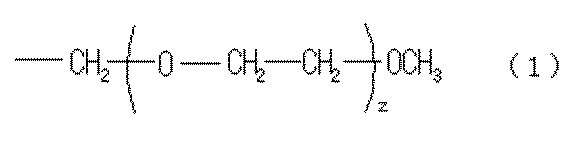


なお、環状オレフィン系樹脂以外の(A)アルカリ可溶性樹脂も、環状オレフィン系樹脂で説明したのと同様の条件を満足するように合成することにより、上記と同様の効果が得られる。
(B)光酸発生剤は、エネルギー線照射による露光時の光反応で酸を生成し、露光部のアルカリ現像液に対する感光性接着剤組成物の溶解性を増加させることができるポジ型の光酸発生剤としての機能を有する。これにより、半導体装置の製造において、感光性接着剤組成物(塗膜601a)のうちの露光された部分である露光部において、現像後の溶け残りが生じることをより低減することができる。このため、現像時のパターンニング性を向上させることができる。なお、感光性接着剤組成物は、(B)光酸発生剤を含むことにより、半導体装置の製造において、エネルギー線照射によって後述する(C)エポキシ化合物による(A)アルカリ可溶性樹脂を架橋させる反応を促進することができるネガ型の光酸発生剤としての機能を有していてもよい。
(C)エポキシ化合物は、(A)アルカリ可溶性樹脂(特に、環状オレフィン系樹脂)を架橋する機能を有する。
感光性接着剤組成物は、(D)融点が50~150℃であるフェノール化合物(以下、単に「(D)フェノール化合物」ということもある。)を含むことにより、例えば、塗膜601aを備えたウエハー201をエッチングする際や、接着層601を介して半導体チップ20同士を圧着する際に、接着層601と半導体チップ20との間に気泡が発生するのを抑制することができる。また、接着層601と半導体チップ20との間に気泡が発生した場合でも、その発生した気泡を除去することができる。このように接着層601と半導体チップ20との界面に気泡が取り残され難くなることで、接着層601の半導体チップ20に対する接着力を高めることができ、よって、半導体チップ20同士を強固に接着することができる。したがって、最終的に、信頼性の高いチップ積層体200を得ることができる。
次に、感光性接着剤組成物の物性(接着層601の物性)について詳細に説明する。
なお、硬化前の感光性接着剤組成物の弾性率も、硬化後の感光性接着剤組成物の弾性率と同様に測定することができる。
(実施例1)
[1](A)アルカリ可溶性樹脂(環状オレフィン系樹脂A-1)の合成
複数のガラス機器を用意し、これらを60℃、0.1トル(Torr)下で18時間乾燥した。その後、全てのガラス機器をグローブボックス内に備え付けた。
は水層と有機層に分離するため、上の層の水層を取り除き、有機層を60℃、15分間、メタノール/脱イオン水(=390g/2376g)溶液で3回洗浄した。そして、得られたポリマーをプロピレングリコールメチルエーテルアセタート中に希釈し、ポリマーの濃度が40%となるように溶媒置換した。このようにして、式(7)で示す、溶液状態のポリマー(環状オレフィン系樹脂A-1)を得た。

前記[1]にて得られた(A)アルカリ可溶性樹脂としての環状オレフィン系樹脂A-1(固形分として22.0質量部)と、(B)光酸発生剤としての光酸発生剤B-1(4.0質量部)と、(C)エポキシ化合物としてのエポキシ化合物C-1(5.0質量部)と、(D)フェノール化合物としてのフェノール化合物D-1(3.0質量部)と、酸化防止剤E-1(2.0質量部)と、酸化防止剤E-2(3.0質量部)と、溶媒(溶剤)としてのプロピレングリコールメチルエーテルアセタート(環状オレフィン系樹脂A-1の溶液に含まれているプロピレングリコールメチルエーテルアセタートも含めて61.0質量部)とを混合し、均一な感光性接着剤組成物を得た。
この実施例1の感光性接着剤組成物で用いた材料を以下に示す。
光酸発生剤B-1として、下記式(8)で表される化合物を用意した。

エポキシ化合物C-1として、下記式(9)で表される化合物を用意した。

フェノール化合物D-1として、下記式(10)で表される化合物(4-ヒドロキシ安息香酸ブチル)を用意した。

酸化防止剤E-1として、下記式(11)で表される化合物(4,4’-ジ(α,α-ジメチルベンジル)ジフェニルアミン)を用意した。

酸化防止剤E-2として、下記式(12)で表される化合物(2,6-ビス[(2-ヒドロキシ-5-メチルフェニル)メチル]-4-メチルフェノール)を用意した。

感光性接着剤組成物を構成する材料を表1および表2に示すように変更し、その各材料の含有量を表1および表2に示すように設定した以外は、実施例1と同様にして感光性接着剤組成物を得た。
なお、各実施例および各比較例の感光性接着剤組成物で用いた材料を以下に示す。
環状オレフィン系樹脂A-2((A)アルカリ可溶性樹脂)として、下記式(13)で表される化合物を用意した。

環状オレフィン系樹脂A-3((A)アルカリ可溶性樹脂)として、下記式(14)で表される化合物を用意した。

フェノール化合物D-2((D)フェノール化合物)として、下記式(15)で表される化合物(4-ヒドロキシ安息香酸ヘキシル)を用意した。

フェノール化合物D-3((D)フェノール化合物)として、下記式(16)で表される化合物(4-ヒドロキシ安息香酸メチル)を用意した。

フェノール化合物D-4((D)フェノール化合物)として、下記式(17)で表される化合物(2-ドデシルフェノール)を用意した。

フェノール化合物D-5((D)フェノール化合物)として、下記式(18)で表される化合物(1,8,9-トリヒドロキシアントラセン)を用意した。

フェノール化合物D-6((D)フェノール化合物)として、下記式(19)で表される化合物(2,2’-ジヒドロキシジフェニルメタン)を用意した。

フェノール化合物X-1((X)フェノール化合物)として、下記式(20)で表される化合物(4,4’-[(2-ヒドロキシフェニル)メチレン]ビス[2-シクロヘキシル-5-メチルフェノール])を用意した。

〈エポキシ化合物C-2〉
エポキシ化合物C-2として、下記式(21)で表される芳香族エポキシ化合物を用意した。

まず、各実施例および各比較例で使用した感光性接着剤組成物をシリコン製の半導体チップ上に塗布し、120℃、5分間のプリベークを行った。これにより、塗膜を得た。
次いで、塗膜を備える半導体チップに対し、エッチング処理およびアッシング処理を順次施した。エッチング処理は、フッ素化合物ガス(CF4)とアルゴンガス(Ar)と酸素ガス(O2)の混合ガスを用い、出力は2500W、時間は6分、CF4流量/Ar流量/O2流量は200sccm/200sccm/50sccmの条件で行った。また、アッシング処理は、O2とArの混合ガスを用い、出力は600W、時間は12分、O2流量は200sccmの条件で行った。
[4.1]接着性の評価
[4.1.1]現像時密着性の評価
まず、各実施例および各比較例で使用した感光性接着剤組成物をシリコン製の半導体チップ上に塗布し、120℃、5分間のプリベークを行った。これにより、厚さ10μmの塗膜を得た。
A :塗膜の全体が、半導体チップから剥がれなかった。
B :塗膜の30%未満が、半導体チップから剥がれた。
C :塗膜の30%以上50%未満が、半導体チップから剥がれた。
D :塗膜の50%以上が、半導体チップから剥がれた。
得られた評価用テストピースについて、Dage4000(デイジ・ジャパン株式会社製)を用い、半導体チップの横(側面)からシェアツールで、一方の半導体チップを水平方向に押し、チップ間の接合面が破断されたときのチップあたりのダイシェア強度を測定した。チップサイズは4mm×4mmであった。
そして、測定したダイシェア強度を、以下の評価基準に基づいて評価した。
A :ダイシェア強度が非常に高い。
B :ダイシェア強度が高い。
C :ダイシェア強度が低い。
D :ダイシェア強度が非常に低い。
まず、各実施例および各比較例で使用した感光性接着剤組成物をシリコン製の半導体チップ上に塗布し、120℃、5分間のプリベークを行った。これにより、塗膜を得た。
次いで、加熱処理後の塗膜が形成された半導体チップを、プロピレングリコール-1-モノメチルエーテル-2-アセタート中に浸漬し、20時間放置した。
A :塗膜の残渣が全く認められない。
B :塗膜の残渣がわずかに認められる。
C :塗膜の残渣が多く認められる。
D :塗膜がほとんど除去されていない。
まず、各実施例および各比較例で使用した感光性接着剤組成物をシリコン製の半導体チップ上に塗布し、120℃、5分間のプリベークを行った。これにより、厚さ10μmの塗膜を得た。
未露光部の残膜率=100×未露光部の現像後の膜厚/プリベーク後の膜厚
露光部の残膜率=100×露光部の現像後の膜厚/プリベーク後の膜厚
求めた露光量を表1に示す。
まず、[4.4]と同様にして、各実施例および各比較例について露光処理を施した塗膜を用意した。次いで、露光処理を施した塗膜に対して現像処理を行った後、150℃、40分間の加熱処理を行った。そして、以下のようにして定義される未露光部の残膜率を求めた。
求めた残膜率を表1に示す。

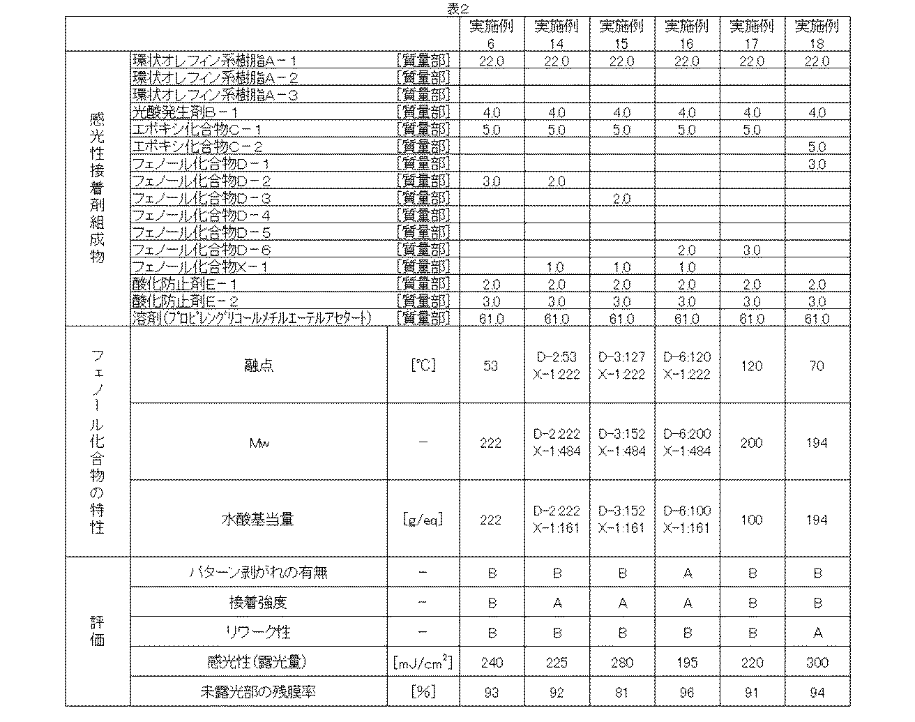
Claims (18)
- (A)アルカリ可溶性樹脂と、
(B)光酸発生剤と、
(C)エポキシ化合物と、
(D)融点が50~150℃であるフェノール化合物と、
を含むことを特徴とする感光性接着剤組成物。 - 前記(D)フェノール化合物より融点が高い(X)フェノール化合物を、さらに含む請求項1に記載の感光性接着剤組成物。
- 前記(X)フェノール化合物は、その融点が151~250℃である請求項2に記載の感光性接着剤組成物。
- 前記(X)フェノール化合物は、複数のフェノール骨格を有するフェノール化合物を含む請求項2または3のいずれか1項に記載の感光性接着剤組成物。
- 前記複数のフェノール骨格を有するフェノール化合物は、環状構造を含む置換基であって、少なくとも1つの前記フェノール骨格に結合した置換基を有する請求項4に記載の感光性接着剤組成物。
- 前記(D)フェノール化合物は、脂肪族炭化水素基を含む置換基を有するフェノール化合物および複数のフェノール骨格を有するフェノール化合物のうちの少なくとも一方を含む請求項1ないし5のいずれか1項に記載の感光性接着剤組成物。
- 前記脂肪族炭化水素基を含む置換基を有するフェノール化合物は、その水酸基当量が150~250g/eqである請求項6に記載の感光性接着剤組成物。
- 前記(D)フェノール化合物の前記複数のフェノール骨格は、連結型の多環構造を形成している請求項6または7に記載の感光性接着剤組成物。
- 前記複数のフェノール骨格を有するフェノール化合物は、その水酸基当量が50~150g/eqである請求項6ないし8のいずれか1項に記載の感光性接着剤組成物。
- 前記(A)アルカリ可溶性樹脂は、環状オレフィン系樹脂を含む請求項1ないし9のいずれか1項に記載の感光性接着剤組成物。
- 前記環状オレフィン系樹脂は、ノルボルネン系樹脂を含む請求項10に記載の感光性接着剤組成物。
- 前記(A)アルカリ可溶性樹脂は、酸性基を有する請求項1ないし11のいずれか1項に記載の感光性接着剤組成物。
- 前記(A)アルカリ可溶性樹脂は、炭素数が2~30の直鎖状の置換基を有する請求項1ないし12のいずれか1項に記載の感光性接着剤組成物。
- 前記直鎖状の置換基は、アルキルエーテル構造を含む請求項13に記載の感光性接着剤組成物。
- 前記直鎖状の置換基は、下記式(1)で示される基である請求項13または14に記載の感光性接着剤組成物。

- 前記(A)アルカリ可溶性樹脂は、前記直鎖状の置換基を有する繰り返し単位を20~60mol%で含む請求項13ないし15のいずれか1項に記載の感光性接着剤組成物。
- 前記(C)エポキシ化合物は、2つ以上のグリシジル基を有する請求項1ないし16のいずれか1項に記載の感光性接着剤組成物。
- 積層型半導体素子を備える半導体装置であって、
前記積層型半導体素子は、複数の半導体素子と、前記半導体素子同士の間に設けられ、これらを接合する請求項1ないし17のいずれか1項に記載の感光性接着剤組成物の硬化物とを有することを特徴とする半導体装置。
Priority Applications (3)
| Application Number | Priority Date | Filing Date | Title |
|---|---|---|---|
| KR1020177010967A KR102355576B1 (ko) | 2014-10-24 | 2015-10-21 | 감광성 접착제 조성물 및 반도체 장치 |
| JP2016555252A JP6702194B2 (ja) | 2014-10-24 | 2015-10-21 | 感光性接着剤組成物および半導体装置 |
| SG11201702930RA SG11201702930RA (en) | 2014-10-24 | 2015-10-21 | Photosensitive adhesive composition and semiconductor device |
Applications Claiming Priority (2)
| Application Number | Priority Date | Filing Date | Title |
|---|---|---|---|
| JP2014-217744 | 2014-10-24 | ||
| JP2014217744 | 2014-10-24 |
Publications (1)
| Publication Number | Publication Date |
|---|---|
| WO2016063909A1 true WO2016063909A1 (ja) | 2016-04-28 |
Family
ID=55760941
Family Applications (1)
| Application Number | Title | Priority Date | Filing Date |
|---|---|---|---|
| PCT/JP2015/079692 Ceased WO2016063909A1 (ja) | 2014-10-24 | 2015-10-21 | 感光性接着剤組成物および半導体装置 |
Country Status (5)
| Country | Link |
|---|---|
| JP (2) | JP6702194B2 (ja) |
| KR (1) | KR102355576B1 (ja) |
| SG (1) | SG11201702930RA (ja) |
| TW (1) | TWI728958B (ja) |
| WO (1) | WO2016063909A1 (ja) |
Cited By (2)
| Publication number | Priority date | Publication date | Assignee | Title |
|---|---|---|---|---|
| WO2021076131A1 (en) * | 2019-10-17 | 2021-04-22 | Promerus, Llc | Photosensitive compositions and applications thereof |
| US20210116807A1 (en) * | 2019-10-17 | 2021-04-22 | Promerus, Llc | Photosensitive compositions and applications thereof |
Families Citing this family (3)
| Publication number | Priority date | Publication date | Assignee | Title |
|---|---|---|---|---|
| CN110461976B (zh) * | 2017-03-30 | 2021-12-24 | 琳得科株式会社 | 粘接片、和层叠体的制造方法 |
| TWI848011B (zh) * | 2019-10-17 | 2024-07-11 | 日商住友電木股份有限公司 | 感光性組成物及其應用 |
| TW202528839A (zh) * | 2023-09-29 | 2025-07-16 | 美商普羅梅勒斯有限公司 | 含有不含pfas的多環烯烴聚合物之感光性組成物及由其製成的半導體裝置 |
Citations (3)
| Publication number | Priority date | Publication date | Assignee | Title |
|---|---|---|---|---|
| JP2005307037A (ja) * | 2004-04-22 | 2005-11-04 | Nagase Chemtex Corp | フィルム状エポキシ樹脂組成物 |
| JP2011155209A (ja) * | 2010-01-28 | 2011-08-11 | Hitachi Chem Co Ltd | 接着剤付半導体チップの製造方法及び半導体装置の製造方法 |
| JP2013122005A (ja) * | 2011-12-09 | 2013-06-20 | Samsung Yokohama Research Institute Co Ltd | 半導体用感光性接着フィルムおよび当該フィルムを用いた半導体装置の製造方法 |
Family Cites Families (4)
| Publication number | Priority date | Publication date | Assignee | Title |
|---|---|---|---|---|
| JP3422691B2 (ja) * | 1997-07-30 | 2003-06-30 | 住友ベークライト株式会社 | ポジ型感光性樹脂組成物 |
| JP4213998B2 (ja) | 2002-05-30 | 2009-01-28 | 三井化学株式会社 | 接着剤樹脂組成物及びそれを用いたフィルム状接着剤 |
| US8530133B2 (en) | 2010-09-28 | 2013-09-10 | Promerus, Llc | Preparation of norbornane-based PAC ballasts |
| TWI632163B (zh) * | 2013-02-04 | 2018-08-11 | 日商日本傑恩股份有限公司 | Radiation-sensitive resin composition and electronic component |
-
2015
- 2015-10-21 JP JP2016555252A patent/JP6702194B2/ja active Active
- 2015-10-21 WO PCT/JP2015/079692 patent/WO2016063909A1/ja not_active Ceased
- 2015-10-21 SG SG11201702930RA patent/SG11201702930RA/en unknown
- 2015-10-21 KR KR1020177010967A patent/KR102355576B1/ko active Active
- 2015-10-23 TW TW104134988A patent/TWI728958B/zh active
-
2020
- 2020-04-28 JP JP2020079208A patent/JP7021685B2/ja active Active
Patent Citations (3)
| Publication number | Priority date | Publication date | Assignee | Title |
|---|---|---|---|---|
| JP2005307037A (ja) * | 2004-04-22 | 2005-11-04 | Nagase Chemtex Corp | フィルム状エポキシ樹脂組成物 |
| JP2011155209A (ja) * | 2010-01-28 | 2011-08-11 | Hitachi Chem Co Ltd | 接着剤付半導体チップの製造方法及び半導体装置の製造方法 |
| JP2013122005A (ja) * | 2011-12-09 | 2013-06-20 | Samsung Yokohama Research Institute Co Ltd | 半導体用感光性接着フィルムおよび当該フィルムを用いた半導体装置の製造方法 |
Cited By (5)
| Publication number | Priority date | Publication date | Assignee | Title |
|---|---|---|---|---|
| WO2021076131A1 (en) * | 2019-10-17 | 2021-04-22 | Promerus, Llc | Photosensitive compositions and applications thereof |
| US20210116807A1 (en) * | 2019-10-17 | 2021-04-22 | Promerus, Llc | Photosensitive compositions and applications thereof |
| US11537045B2 (en) | 2019-10-17 | 2022-12-27 | Promerus, Llc | Photosensitive compositions and applications thereof |
| JP2023506116A (ja) * | 2019-10-17 | 2023-02-15 | プロメラス, エルエルシー | 感光性組成物およびその用途 |
| JP7447252B2 (ja) | 2019-10-17 | 2024-03-11 | プロメラス, エルエルシー | 感光性組成物およびその用途 |
Also Published As
| Publication number | Publication date |
|---|---|
| SG11201702930RA (en) | 2017-05-30 |
| KR20170076674A (ko) | 2017-07-04 |
| JP7021685B2 (ja) | 2022-02-17 |
| JP6702194B2 (ja) | 2020-05-27 |
| TWI728958B (zh) | 2021-06-01 |
| JP2020128545A (ja) | 2020-08-27 |
| JPWO2016063909A1 (ja) | 2017-08-10 |
| TW201623533A (zh) | 2016-07-01 |
| KR102355576B1 (ko) | 2022-01-25 |
Similar Documents
| Publication | Publication Date | Title |
|---|---|---|
| JP7021685B2 (ja) | 感光性接着剤組成物および半導体装置 | |
| JP6299389B2 (ja) | 感光性接着剤組成物および半導体装置 | |
| JP2000298352A (ja) | 電子部品用材料およびその使用方法 | |
| KR20190037268A (ko) | 무수나드산 중합체 및 그로부터 유래한 감광성 조성물 | |
| US20160223908A1 (en) | Photosensitive compositions and applications thereof | |
| JP6528421B2 (ja) | 感光性樹脂組成物 | |
| JP2016086073A (ja) | 半導体装置の製造方法 | |
| JP2018146964A (ja) | 感光性樹脂組成物、パターン硬化物の製造方法、硬化物、層間絶縁膜、カバーコート層、表面保護膜及び電子部品 | |
| JP2021113993A (ja) | 感光性樹脂組成物、半導体装置の製造方法、樹脂膜、硬化樹脂膜、および半導体装置 | |
| JP2019113690A (ja) | 感光性接着剤組成物および構造体 | |
| WO2016063908A1 (ja) | 感光性接着剤組成物および半導体装置 | |
| JP2014225662A (ja) | 感光性接着剤組成物および半導体装置 | |
| WO2019044817A1 (ja) | ネガ型感光性樹脂組成物、半導体装置および電子機器 | |
| JP2018173471A (ja) | 感光性樹脂組成物および半導体装置 | |
| JP6707854B2 (ja) | ポジ型感光性樹脂組成物、硬化膜、保護膜、絶縁膜および電子装置 | |
| JP5338459B2 (ja) | 感光性樹脂組成物、および半導体装置 | |
| JP2023155261A (ja) | 感光性樹脂組成物、電子デバイスの製造方法および電子デバイス | |
| JP6988121B2 (ja) | 感光性樹脂組成物及び半導体装置 | |
| US20250138422A1 (en) | Photosensitive resin composition, manufacturing method of electronic device, and electronic device | |
| US20250110399A1 (en) | Photosensitive composition containing pfas-free polycycloolefinic terpolymers and semiconductor device made thereof | |
| US20250110403A1 (en) | Photosensitive composition containing pfas-free polycycloolefinic polymers and semiconductor device made thereof | |
| EP4045564A1 (en) | Photosensitive compositions and applications thereof | |
| JP7408992B2 (ja) | 感光性樹脂組成物および電子デバイスの製造方法 | |
| JP2014010156A (ja) | 感光性樹脂組成物、それを用いたパターン硬化膜の製造方法及び電子部品 | |
| KR20130115747A (ko) | 후막용 감광성 폴리머 수지 및 이를 포함하는 수지 조성물 |
Legal Events
| Date | Code | Title | Description |
|---|---|---|---|
| 121 | Ep: the epo has been informed by wipo that ep was designated in this application |
Ref document number: 15852634 Country of ref document: EP Kind code of ref document: A1 |
|
| ENP | Entry into the national phase |
Ref document number: 2016555252 Country of ref document: JP Kind code of ref document: A |
|
| WWE | Wipo information: entry into national phase |
Ref document number: 11201702930R Country of ref document: SG |
|
| ENP | Entry into the national phase |
Ref document number: 20177010967 Country of ref document: KR Kind code of ref document: A |
|
| NENP | Non-entry into the national phase |
Ref country code: DE |
|
| 122 | Ep: pct application non-entry in european phase |
Ref document number: 15852634 Country of ref document: EP Kind code of ref document: A1 |