WO2016039345A1 - 撮像素子および内視鏡装置 - Google Patents
撮像素子および内視鏡装置 Download PDFInfo
- Publication number
- WO2016039345A1 WO2016039345A1 PCT/JP2015/075487 JP2015075487W WO2016039345A1 WO 2016039345 A1 WO2016039345 A1 WO 2016039345A1 JP 2015075487 W JP2015075487 W JP 2015075487W WO 2016039345 A1 WO2016039345 A1 WO 2016039345A1
- Authority
- WO
- WIPO (PCT)
- Prior art keywords
- light
- substrate
- pixel
- junction surface
- wavelength band
- Prior art date
- Legal status (The legal status is an assumption and is not a legal conclusion. Google has not performed a legal analysis and makes no representation as to the accuracy of the status listed.)
- Ceased
Links
Images


Classifications
-
- A—HUMAN NECESSITIES
- A61—MEDICAL OR VETERINARY SCIENCE; HYGIENE
- A61B—DIAGNOSIS; SURGERY; IDENTIFICATION
- A61B1/00—Instruments for performing medical examinations of the interior of cavities or tubes of the body by visual or photographical inspection, e.g. endoscopes; Illuminating arrangements therefor
- A61B1/04—Instruments for performing medical examinations of the interior of cavities or tubes of the body by visual or photographical inspection, e.g. endoscopes; Illuminating arrangements therefor combined with photographic or television appliances
- A61B1/043—Instruments for performing medical examinations of the interior of cavities or tubes of the body by visual or photographical inspection, e.g. endoscopes; Illuminating arrangements therefor combined with photographic or television appliances for fluorescence imaging
-
- A—HUMAN NECESSITIES
- A61—MEDICAL OR VETERINARY SCIENCE; HYGIENE
- A61B—DIAGNOSIS; SURGERY; IDENTIFICATION
- A61B1/00—Instruments for performing medical examinations of the interior of cavities or tubes of the body by visual or photographical inspection, e.g. endoscopes; Illuminating arrangements therefor
- A61B1/04—Instruments for performing medical examinations of the interior of cavities or tubes of the body by visual or photographical inspection, e.g. endoscopes; Illuminating arrangements therefor combined with photographic or television appliances
- A61B1/042—Instruments for performing medical examinations of the interior of cavities or tubes of the body by visual or photographical inspection, e.g. endoscopes; Illuminating arrangements therefor combined with photographic or television appliances characterised by a proximal camera, e.g. a CCD camera
-
- G—PHYSICS
- G02—OPTICS
- G02B—OPTICAL ELEMENTS, SYSTEMS OR APPARATUS
- G02B23/00—Telescopes, e.g. binoculars; Periscopes; Instruments for viewing the inside of hollow bodies; Viewfinders; Optical aiming or sighting devices
- G02B23/24—Instruments or systems for viewing the inside of hollow bodies, e.g. fibrescopes
- G02B23/2407—Optical details
- G02B23/2423—Optical details of the distal end
-
- G—PHYSICS
- G02—OPTICS
- G02B—OPTICAL ELEMENTS, SYSTEMS OR APPARATUS
- G02B23/00—Telescopes, e.g. binoculars; Periscopes; Instruments for viewing the inside of hollow bodies; Viewfinders; Optical aiming or sighting devices
- G02B23/24—Instruments or systems for viewing the inside of hollow bodies, e.g. fibrescopes
- G02B23/2407—Optical details
- G02B23/2453—Optical details of the proximal end
-
- G—PHYSICS
- G02—OPTICS
- G02B—OPTICAL ELEMENTS, SYSTEMS OR APPARATUS
- G02B23/00—Telescopes, e.g. binoculars; Periscopes; Instruments for viewing the inside of hollow bodies; Viewfinders; Optical aiming or sighting devices
- G02B23/24—Instruments or systems for viewing the inside of hollow bodies, e.g. fibrescopes
- G02B23/2476—Non-optical details, e.g. housings, mountings, supports
- G02B23/2484—Arrangements in relation to a camera or imaging device
-
- H—ELECTRICITY
- H04—ELECTRIC COMMUNICATION TECHNIQUE
- H04N—PICTORIAL COMMUNICATION, e.g. TELEVISION
- H04N23/00—Cameras or camera modules comprising electronic image sensors; Control thereof
- H04N23/10—Cameras or camera modules comprising electronic image sensors; Control thereof for generating image signals from different wavelengths
- H04N23/11—Cameras or camera modules comprising electronic image sensors; Control thereof for generating image signals from different wavelengths for generating image signals from visible and infrared light wavelengths
-
- H—ELECTRICITY
- H04—ELECTRIC COMMUNICATION TECHNIQUE
- H04N—PICTORIAL COMMUNICATION, e.g. TELEVISION
- H04N23/00—Cameras or camera modules comprising electronic image sensors; Control thereof
- H04N23/10—Cameras or camera modules comprising electronic image sensors; Control thereof for generating image signals from different wavelengths
- H04N23/12—Cameras or camera modules comprising electronic image sensors; Control thereof for generating image signals from different wavelengths with one sensor only
-
- H—ELECTRICITY
- H04—ELECTRIC COMMUNICATION TECHNIQUE
- H04N—PICTORIAL COMMUNICATION, e.g. TELEVISION
- H04N23/00—Cameras or camera modules comprising electronic image sensors; Control thereof
- H04N23/56—Cameras or camera modules comprising electronic image sensors; Control thereof provided with illuminating means
-
- H—ELECTRICITY
- H10—SEMICONDUCTOR DEVICES; ELECTRIC SOLID-STATE DEVICES NOT OTHERWISE PROVIDED FOR
- H10F—INORGANIC SEMICONDUCTOR DEVICES SENSITIVE TO INFRARED RADIATION, LIGHT, ELECTROMAGNETIC RADIATION OF SHORTER WAVELENGTH OR CORPUSCULAR RADIATION
- H10F39/00—Integrated devices, or assemblies of multiple devices, comprising at least one element covered by group H10F30/00, e.g. radiation detectors comprising photodiode arrays
- H10F39/10—Integrated devices
- H10F39/12—Image sensors
- H10F39/18—Complementary metal-oxide-semiconductor [CMOS] image sensors; Photodiode array image sensors
- H10F39/182—Colour image sensors
- H10F39/1825—Multicolour image sensors having stacked structure, e.g. NPN, NPNPN or multiple quantum well [MQW] structures
-
- H—ELECTRICITY
- H10—SEMICONDUCTOR DEVICES; ELECTRIC SOLID-STATE DEVICES NOT OTHERWISE PROVIDED FOR
- H10F—INORGANIC SEMICONDUCTOR DEVICES SENSITIVE TO INFRARED RADIATION, LIGHT, ELECTROMAGNETIC RADIATION OF SHORTER WAVELENGTH OR CORPUSCULAR RADIATION
- H10F39/00—Integrated devices, or assemblies of multiple devices, comprising at least one element covered by group H10F30/00, e.g. radiation detectors comprising photodiode arrays
- H10F39/10—Integrated devices
- H10F39/12—Image sensors
- H10F39/18—Complementary metal-oxide-semiconductor [CMOS] image sensors; Photodiode array image sensors
- H10F39/184—Infrared image sensors
-
- H—ELECTRICITY
- H10—SEMICONDUCTOR DEVICES; ELECTRIC SOLID-STATE DEVICES NOT OTHERWISE PROVIDED FOR
- H10F—INORGANIC SEMICONDUCTOR DEVICES SENSITIVE TO INFRARED RADIATION, LIGHT, ELECTROMAGNETIC RADIATION OF SHORTER WAVELENGTH OR CORPUSCULAR RADIATION
- H10F39/00—Integrated devices, or assemblies of multiple devices, comprising at least one element covered by group H10F30/00, e.g. radiation detectors comprising photodiode arrays
- H10F39/80—Constructional details of image sensors
- H10F39/805—Coatings
- H10F39/8053—Colour filters
-
- H—ELECTRICITY
- H10—SEMICONDUCTOR DEVICES; ELECTRIC SOLID-STATE DEVICES NOT OTHERWISE PROVIDED FOR
- H10F—INORGANIC SEMICONDUCTOR DEVICES SENSITIVE TO INFRARED RADIATION, LIGHT, ELECTROMAGNETIC RADIATION OF SHORTER WAVELENGTH OR CORPUSCULAR RADIATION
- H10F39/00—Integrated devices, or assemblies of multiple devices, comprising at least one element covered by group H10F30/00, e.g. radiation detectors comprising photodiode arrays
- H10F39/80—Constructional details of image sensors
- H10F39/809—Constructional details of image sensors of hybrid image sensors
-
- H—ELECTRICITY
- H04—ELECTRIC COMMUNICATION TECHNIQUE
- H04N—PICTORIAL COMMUNICATION, e.g. TELEVISION
- H04N23/00—Cameras or camera modules comprising electronic image sensors; Control thereof
- H04N23/50—Constructional details
- H04N23/555—Constructional details for picking-up images in sites, inaccessible due to their dimensions or hazardous conditions, e.g. endoscopes or borescopes
Definitions
- the present invention relates to an imaging device and an endoscope apparatus.
- Priority is claimed on Japanese Patent Application No. 2014-183211, filed September 09, 2014, the content of which is incorporated herein by reference.
- ICG indocyanine green
- FIG. 14 is a block diagram showing the configuration of a conventionally known fluorescence endoscope apparatus capable of simultaneously capturing a normal visible image and an infrared image of the fluorescence wavelength of ICG.
- the fluorescence endoscope apparatus 1 ⁇ / b> A uses the dichroic mirror 22 to make visible light incident on the RGB imaging elements 26, 27, 28. As a result, the RGB imaging elements 26, 27 and 28 generate image signals.
- the infrared light component is reflected by the dichroic mirror 22, passes through the excitation light cut filter 23, and is incident on the infrared imaging element 25. Thereby, the infrared imaging device 25 generates an ICG fluorescence image signal.
- FIG. 15 is a graph showing the characteristics of the band pass filter 12 disposed in the light source device 3A of the conventionally known fluorescence endoscope apparatus 1A.
- a line 1501 is a line indicating the transmittance of the band pass filter 12. Due to this characteristic, the band pass filter 12 transmits the visible component of the light of the xenon light source 11 and the excitation wavelength component of the ICG fluorescent material, and illuminates the subject.
- FIG. 16 is a graph showing the characteristics of the dichroic mirror 22 of the conventionally known fluorescence endoscope apparatus 1A.
- a line 1601 is a line indicating the transmittance of the dichroic mirror 22. Due to this characteristic, the dichroic mirror 22 is configured to transmit the visible component and reflect the infrared component.
- FIG. 17 is a graph showing the characteristics of the excitation light cut filter 23 of the conventionally known fluorescence endoscope apparatus 1A.
- a line 1701 is a line indicating the transmittance of the excitation light cut filter 23. Due to this characteristic, the excitation light cut filter 23 is configured to transmit only the component having a wavelength longer than the fluorescence wavelength of the ICG fluorescent substance, and allow the infrared imaging device 25 to capture only a fluorescence image.
- FIG. 18 is a graph showing the characteristics of excitation wavelength and fluorescence wavelength of a conventionally known ICG fluorescent substance.
- a line 1801 is a line indicating the intensity of the excitation light.
- a line 1802 is a line indicating the intensity of fluorescence. In order to generate an ICG fluorescence image signal, it is necessary to remove the excitation wavelength component irradiated to the subject by the light source and to image the light of only the fluorescence wavelength component with the imaging device.
- the fluorescence endoscope apparatus 1A can separate visible and infrared light by the dichroic mirror 22 and transmit the excitation cut filter 23 to simultaneously capture a visible image and a fluorescent image.
- the fluorescence endoscope apparatus 1A is a system capable of irradiating a subject with light of a visible component from the light source device 3A and light of an excitation light component from the laser light source 7 to be imaged.
- FIG. 19 is a cross-sectional view showing a conventionally known image pickup device of a hybrid structure in which two layers of image pickup devices are stacked and light is transmitted through the upper layer to perform imaging also in the lower layer.
- the first substrate 221 and the second substrate 222 are stacked.
- First photodiodes 223-1 to 223-n are formed on the upper first substrate 221.
- Second photodiodes 224-1 to 224-n are formed on the lower second substrate 222.
- the first substrate is made a thin image sensor like BSI in the hybrid PD-PD imager as shown in FIG. 19, the long wavelength component like the ICG fluorescence wavelength shown in the graph of FIG. It can be transmitted and imaged by the second substrate 222.
- the dichroic mirror is not required compared to the configuration shown in FIG. 14, and the camera head can be miniaturized.
- FIG. 20 is a graph showing conventionally known ICG fluorescence characteristics and characteristics of a laminated imaging device.
- a line 1081 is a line indicating a transmission rate of excitation light.
- a line 1082 is a line indicating the transmission rate of fluorescence.
- a line 1083 is a line indicating the transmission rate of light transmitted through the first substrate 221.
- the light transmitted through the first substrate 221 is greatly attenuated at 600 to 800 nm, an unignorable amount of light reaches the lower layer.
- the light with a wavelength of 600 to 800 nm is unnecessary for imaging with the second substrate 222 for the purpose of detecting the fluorescence wavelength of the ICG.
- arranging a color filter that cuts light of 800 nm or less between the layers of the first substrate 221 and the second substrate 222 has a problem of difficulty in manufacturing.
- the present invention has been made to solve the above problems, and provides an imaging device and an endoscope apparatus capable of imaging a fluorescence image corresponding to a wavelength of interest with high accuracy in an imaging device of a hybrid structure.
- the purpose is to
- a first substrate a second substrate stacked on the first substrate, and a first light receiving element disposed in a matrix on the first substrate and having a visible band.
- Incident light in a second wavelength band including a first wavelength band including and a near-infrared band longer in wavelength than the first wavelength band, and generating a first signal according to the light in the first wavelength band
- a second pixel arranged in a matrix on the second substrate and irradiated with the light transmitted through the first pixel, wherein the second pixel is connected to a first PN junction surface parallel to the light receiving surface.
- a second PN junction surface parallel to the light receiving surface and at a deeper position than the first PN junction surface, and a charge corresponding to the light of the second wavelength band from the charge obtained at the second PN junction surface 2 Generate a signal.
- Incident light of a first wavelength band including and a second wavelength band including a near-infrared band longer in wavelength than the first wavelength band is irradiated to generate a first signal according to the light of the first wavelength band
- a second PN junction surface which is parallel to the light receiving surface and deeper than the first PN junction surface, and the charge obtained at the second PN junction surface corresponds to the light of the second wavelength band.
- the first PN junction surface generates charges with light including a wavelength of the first wavelength band. Good.
- the P-type layer and the N-type layer of the first PN junction surface are connected at the same potential. Good.
- the first signal is corrected using the third signal generated at the first PN junction surface.
- the light is incident on the first pixel and the second pixel using the third signal. You may control the light quantity of light.
- a seventh aspect of the present invention there is provided a first substrate, a second substrate stacked on the first substrate, and a first light receiving element which is disposed in a matrix on the first substrate and has a visible band. And the incident light of the second wavelength band including the near-infrared region whose wavelength is longer than the first wavelength band is irradiated, and the first signal according to the light of the first wavelength band is emitted.
- a second pixel arranged in a matrix on the second substrate and irradiated with light transmitted through the first pixel, the second pixel being parallel to the light receiving surface
- a second signal according to light is generated, and the first pixel includes a third PN junction surface parallel to the light receiving surface, the light receiving surface, and A fourth PN junction surface existing at a position deeper than the third PN junction surface in a row, and generating a fourth signal corresponding to the light of the second wavelength band from the charge obtained at the fourth PN junction surface .
- An eighth aspect of the present invention is an endoscope apparatus which performs diagnosis by an endoscope by administering a fluorescent substance comprising an indocyanine green derivative-labeled antibody to an object to be examined, the first to seventh aspects to the seventh aspect.
- An imaging device according to any one of the embodiments, wherein a visible light band and a near infrared fluorescence wavelength band of the fluorescent material are transmitted to the light receiving surface side of the first pixel, and an excitation wavelength band close to the fluorescence wavelength band
- An optical filter which does not transmit the component is disposed, the first wavelength band includes a visible band, and the second wavelength band includes a fluorescent band of a fluorescent substance.
- a first image of a visible band is created from the first signal, and a second image of a fluorescence wavelength band is generated from the second signal.
- the first substrate, the second substrate, and the optical filter may be disposed at a distal end portion of the endoscope.
- the first substrate, the second substrate stacked on the first substrate, and the first substrate are arranged in a matrix, and each have the first light receiving element.
- the incident light of the first wavelength band including the visible band and the incident light of the second wavelength band including the near-infrared area whose wavelength is longer than the first wavelength band are irradiated, and the first corresponding to the light of the first wavelength band
- a second pixel arranged in a matrix on the second substrate and irradiated with the light transmitted through the first pixel.
- the second pixel has a first PN junction surface parallel to the light receiving surface, and a second PN junction surface parallel to the light receiving surface and at a deeper position than the first PN junction surface, and is obtained by the second PN junction surface.
- a second signal corresponding to the light of the second wavelength band is generated from the charge. Therefore, a fluorescence image corresponding to the wavelength of interest can be captured with high accuracy in the hybrid-structured imaging device.
- characteristics of excitation light, fluorescence, light transmitted through the first substrate, light detected by the first PN junction surface, and light detected by the second PN junction surface are shown.
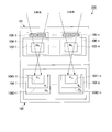
- FIG. 1 is a cross-sectional view showing a cross section of the imaging device 100 in the present embodiment.
- the imaging device 100 includes a first substrate 101, a second substrate 102, first photodiodes 103-1 to 103-n (first light receiving elements), and second pixels 104-1 to 104-. n (second photodiode, second light receiving element) and color filters 105-1 to 105-n.
- the surface on the side to which incident light is irradiated is defined as a light receiving surface.
- the first substrate 101 and the second substrate 102 are stacked.
- the first substrate 101 and the second substrate 102 are silicon substrates.
- the first substrate 101 transmits a part of light of the incident light.
- the first photodiodes 103-1 to 103-n are disposed in the first substrate 101.
- the color filters 105-1 to 105-n are either filters that transmit red light (R), filters that transmit green light (G), or filters that transmit blue light (B). And are disposed on the light receiving surface side of the first photodiodes 103-1 to 103-n. That is, on-chip RGB color filters 105-1 to 105-n are disposed on the first photodiodes 103-1 to 103-n. The arrangement of the color filters 105-1 to 105-n will be described later.
- the color filters 105-1 to 105-n are filters that transmit blue light regardless of whether they are filters (R) that transmit red light or filters (G) that transmit green light. Even in the case of (B), light of infrared wavelength is also transmitted. Also, in general, although an IR cut filter (infrared light cut filter) is provided on the light receiving surface side in an image pickup device for digital cameras and the like, an IR cut filter is not used in this embodiment.
- a set of each of the first photodiodes 103-1 to 103-n and each of the color filters 105-1 to 105-n is referred to as a first pixel 106-1 to 106-n.
- a set of the first photodiode 103-1 and the color filter 105-1 is taken as a first pixel 106-1.
- the first photodiodes 103-1 to 103-n output a first signal according to the exposure amount.
- the second pixels 104-1 to 104-n are disposed in the second substrate 102.
- the second pixels 104-1 to 104-n each include a P-type layer P11 to P1n, an N-type layer N1 to Nn, and a P-type layer P21 to P2n, and Parallel first PN junction surfaces 1041-1 to 1041-n and second PN junction surfaces 1042-1 to 1042-n parallel to the light receiving surface and located deeper than the first PN junction surfaces 1041-1 to 1041-n Have.
- the second pixels 104-1 to 104-n generate the second signal from the charges obtained at the second PN junction surfaces 1042-1 to 1042-n.
- the second pixels 104-1 to 104-n generate a third signal from the charges obtained at the first PN junction surfaces 1041-1 to 1041-n.
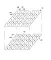
- FIG. 2 is a schematic view showing the arrangement of the color filters 105 in the present embodiment.
- the first substrate 101 includes a total of 36 first pixels 106 regularly arranged in a two-dimensional form of six rows and six columns.
- the second substrate 102 includes a total of 36 second pixels 104 regularly arranged in a two-dimensional form of six rows and six columns.
- color filters 105 color filters R, color filters G, and color filters B are arranged in a Bayer arrangement.
- the first pixel 106 is irradiated with incident light of a first wavelength band including a visible band and a second wavelength band including a near infrared band having a wavelength longer than the first wavelength band, and the first pixel 106 responds to the light of the first wavelength band.
- the second pixel 104 is irradiated with light transmitted through the first pixel 106, for example, light including infrared light.
- Such pixel arrangement makes it possible to simultaneously capture a visible image on the first substrate 101 and an infrared image on the second substrate 102.
- the number of first pixels 106 included in the first substrate 101 and the number of second pixels 104 included in the second substrate 102 are not limited to the example shown in FIG. 2, and any number may be used.
- the arrangement with the two pixels 104 may be any arrangement.
- the second pixel 104 is arranged corresponding to the lower side of the first pixel 106, but the present invention is not limited to this.
- the second pixel 104 is smaller than the first pixel 106 in pixel size. It is also possible to devise an integral multiple or the like.
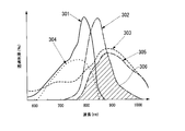
- FIG. 3 shows the excitation light, the fluorescence, the light passing through the first substrate 101, the light detected by the first PN junction surfaces 1041-1 to 1041-n, and the second PN junction surface 1042-1 in the present embodiment.
- FIG. 16 is a graph showing characteristics of light detected by ⁇ 1042-n.
- the horizontal axis of the graph indicates the wavelength (nm).
- the vertical axis of the graph indicates the transmission rate (%).
- a line 301 is a line indicating the characteristics of the excitation light.
- the line 302 is a line showing the characteristic of fluorescence.
- a line 303 is a line indicating the characteristic of light transmitted through the first substrate 101.
- a line 304 is a line indicating the characteristics of light detected by the first PN junction surfaces 1041-1 to 1041-n.
- a line 305 is a line indicating the characteristics of light detected by the second PN junction surfaces 1042-1 to 1042-n.
- the second pixels 104 disposed on the second substrate 102 are present at positions deeper than the first PN junction surfaces 1041-1 to 1041-n and the first PN junction surfaces 1041-1 to 1041-n. And second PN junction surfaces 1042-1 to 1042-n.
- the second PN junction surfaces 1042-1 to 1042-n detect the light transmitted through the first substrate 101 and the first PN junction surfaces 1041-1 to 1041-n (light in the region 306 in FIG. 3). can do.
- the second PN junction surfaces 1042-1 to 1042-n are unnecessary excitation light components (600 to 800 nm) at the first substrate 101 and the first PN junction surfaces 1041-1 to 1041-n existing in the layer on the shallow side.
- the fluorescence component excluding more of the light of the wavelength of (1) can be detected, and the second signal corresponding to the light of the second wavelength band can be generated. Therefore, the imaging device 100 can remove the excitation light component irradiated to the fluorescent material and the visible component, and can obtain an image of the wavelength of interest (fluorescent wavelength (860 nm)) with high S / N.
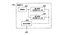
- FIG. 4 is a block diagram showing the configuration of the imaging device 100 in the present embodiment.
- the imaging device 100 includes a driving unit 401, a first pixel / signal reading unit 402, a second pixel / signal reading unit 403, a signal processing unit 404, and a signal output terminal 405.
- the driving unit 401 transmits a control signal to drive the first pixel / signal reading unit 402 and the second pixel / signal reading unit 403.
- the first pixel / signal readout unit 402 includes the first pixels 106-1 to 106-n, reads out the first signal generated by the first pixels 106-1 to 106-n, and outputs the first signal to the signal processing unit 404.
- the second pixel / signal readout unit 403 includes the second pixels 104-1 to 104, reads out the second signal generated by the second pixels 104-1 to 104-n, and outputs the second signal to the signal processing unit 404.
- the signal processing unit 404 generates a first image based on the first signal input from the first pixel / signal readout unit 402.
- the first signal is an R signal according to the intensity of red light, a G signal according to the intensity of green light, and a B signal according to the intensity of blue light. That is, the first signal is an RGB signal. Therefore, the first image generated by the signal processing unit 404 is an RGB image.
- the signal processing unit 404 generates a second image based on the second signal input from the second pixel / signal readout unit 403.
- the second signal is a fluorescence signal according to the intensity of light centered at 830 nm.
- the second image generated by the signal processing unit 404 is a fluorescence image.
- the signal processing unit 404 outputs the generated first image and second image from the signal output terminal 405.
- the signal processing unit 404 may perform image processing such as noise reduction, superimposition of an RGB image, or a fluorescence image, for example.
- FIG. 5 is a timing chart showing drive timings of the image sensor 100 in the present embodiment.
- a timing chart 501 showing the driving timing of the first pixel 106 and a timing chart 502 showing the driving timing of the second pixel 104 are shown.
- the horizontal axis of the timing chart is time.
- the charge accumulation time (exposure time) of the first pixel 106 is longer than the charge accumulation time (exposure time) of the second pixel 104.
- the readout time which is the time for reading out the signal from each pixel, is set such that the frame rates of the RGB image and the fluorescence image become the same frame rate.
- the first substrate 101 and the second substrate 102 are stacked.
- the second substrate 102 is disposed at a position overlapping with the first substrate 101 and on the opposite side of the light receiving surface of the first substrate 101 when viewed from the light receiving surface side of the first substrate 101.
- the first substrate 101 transmits light.
- the light transmitted through the first substrate 101 is irradiated to the second substrate 102.
- the first pixels 106 of the first substrate 101 and the second pixels 104 of the second substrate 102 can be exposed simultaneously. That is, the generation of the first signal by the first pixel 106 and the generation of the second signal by the second pixel 104 can be performed simultaneously. Therefore, the signal processing unit 404 can simultaneously generate a first image (RGB image) based on the first signal and a second image (fluorescent image) based on the second signal.
- a first image RGB image
- a second image fluorescent image
- the second pixel 104 disposed on the second substrate 102 is deeper than the first PN junction surfaces 1041-1 to 1041-n and the first PN junction surfaces 1041-1 to 1041-n. And the second PN junction faces 1042-1 to 1042-n present in position. With this configuration, the second PN junction surfaces 1042-1 to 1042-n can detect light transmitted through the first substrate 101 and the first PN junction surfaces 1041-1 to 1041-n.
- the second PN junction surfaces 1042-1 to 1042-n have more components of unnecessary light at the first substrate 101 and the first PN junction surfaces 1041-1 to 1041-n present in the shallow side layer.
- the removed fluorescent component can be detected to generate a second signal according to the light in the second wavelength band. Therefore, the imaging device 100 can remove the excitation light component irradiated to the fluorescent material and the visible component, and can capture a fluorescence image corresponding to the wavelength of interest with high accuracy.
- the difference between the imaging device 100 in the first embodiment and the imaging device in the present embodiment is the configuration of the first photodiode of the first substrate.
- the other configuration is the same as that of the first embodiment.
- FIG. 6 is a cross-sectional view showing a cross section of the imaging device 600 in the present embodiment.
- the imaging device 600 includes a first substrate 601, a second substrate 102, first photodiodes 603-1 to 603-n (first light receiving elements), and second pixels 104-1 to 104-. n (second photodiode, second light receiving element) and color filters 105-1 to 105-n.
- the surface on the side to which incident light is irradiated is defined as a light receiving surface.
- the first substrate 601 and the second substrate 102 are stacked.
- the first substrate 601 and the second substrate 102 are silicon substrates.
- the first substrate 601 transmits a part of light of the incident light.
- the first photodiodes 603-1 to 603-n are disposed in the first substrate 601.
- the first photodiodes 603-1 to 603-n each include 1P11 to 1P1n which is a P-type layer, 1N1 to 1Nn which is an N-type layer, and 1P21 to 1P2n which is a P-type layer.
- a second PN junction surface 6032-1 to 6032-n parallel to the light receiving surface and at a position deeper than the first PN junction surface 6031-1 to 6031-n.
- the first photodiodes 603-1 to 603-n generate a second signal from the charges obtained at the second PN junction surfaces 6032-1 to 6032-n.
- the first photodiodes 603-1 to 603-n generate a first signal from the charges obtained at the first PN junction surfaces 6031-1 to 6031-n.
- the color filters 105-1 to 105-n are either filters that transmit red light (R), filters that transmit green light (G), or filters that transmit blue light (B). And are disposed on the light receiving surface side of the first photodiodes 603-1 to 603-n. That is, on-chip RGB color filters 105-1 to 105-n are disposed on the first photodiodes 603-1 to 603-n. The arrangement of the color filters 105-1 to 105-n is the same as that of the first embodiment.
- a set of each of the first photodiodes 603-1 to 603-n and each of the color filters 105-1 to 105-n is taken as a first pixel 606-1 to 606-n.
- a set of the first photodiode 603-1 and the color filter 105-1 is taken as a first pixel 606-1.
- the second pixels 104-1 to 104-n are disposed in the second substrate 102.
- the second pixels 104-1 to 104-n each include a P-type layer P11 to P1n, an N-type layer N1 to Nn, and a P-type layer P21 to P2n, and Parallel first PN junction surfaces 1041-1 to 1041-n and second PN junction surfaces 1042-1 to 1042-n parallel to the light receiving surface and located deeper than the first PN junction surfaces 1041-1 to 1041-n Have.
- the second pixels 104-1 to 104-n generate the second signal from the charges obtained at the second PN junction surfaces 1042-1 to 1042-n.
- the second pixels 104-1 to 104-n generate a third signal from the charges obtained at the first PN junction surfaces 1041-1 to 1041-n.
- FIG. 7 is a graph showing the characteristics of excitation light, fluorescence, light transmitted through the first substrate 101, and light detected by the second PN junction surfaces 1042-1 to 1042-n in the present embodiment. .
- the horizontal axis of the graph indicates the wavelength (nm).
- the vertical axis of the graph indicates the transmission rate (%).
- a line 701 is a line indicating the characteristics of the excitation light.
- the line 702 is a line showing the characteristic of fluorescence.
- a line 703 is a line indicating the characteristic of light transmitted through the first substrate 601.
- a line 704 is a line indicating the characteristics of light detected by the second PN junction surfaces 1042-1 to 1042-n.
- the first photodiodes 603-1 to 603-n include 1P11 to 1P1n which are P-type layers, 1N1 to 1Nn which are N-type layers, and 1P21 to 1P2n which are P-type layers, respectively.
- the second PN junction surfaces 1042-1 to 1042-n have fluorescence excluding unnecessary light components at the first PN junction surfaces 1041-1 to 1041-n present in the first substrate 601 and the layer on the shallow side.
- the component can be detected to generate a second signal according to the light of the second wavelength band. Therefore, the imaging device 600 can remove the excitation light component irradiated to the fluorescent material and the visible component, and can capture a fluorescence image corresponding to the wavelength of interest with high accuracy.
- the difference between the imaging device 100 according to the first embodiment and the imaging device according to the present embodiment is that the P-type layer and the N-type layer of the first PN junction surface included in the second pixel are electrically connected It is the point which makes it an electric potential.
- the other configuration is the same as that of the first embodiment.
- FIG. 8 is a cross-sectional view showing a cross section of the image sensor 800 in the present embodiment.
- the imaging device 800 includes a first substrate 101, a second substrate 802, first photodiodes 103-1 to 103-n (first light receiving elements), and second pixels 804-1 to 804-i. And 804-n (second photodiode, second light receiving element) and color filters 105-1 to 105-n.
- the surface on the side to which incident light is irradiated is defined as a light receiving surface.
- the first substrate 101 and the second substrate 802 are stacked.
- the first substrate 101 and the second substrate 802 are silicon substrates.
- the first substrate 101 transmits a part of light of the incident light.
- the first photodiodes 103-1 to 103-n are disposed in the first substrate 101.
- the color filters 105-1 to 105-n are either filters that transmit red light (R), filters that transmit green light (G), or filters that transmit blue light (B). And are disposed on the light receiving surface side of the first photodiodes 103-1 to 103-n. That is, on-chip RGB color filters 105-1 to 105-n are disposed on the first photodiodes 103-1 to 103-n.
- the arrangement of the color filters 105-1 to 105-n is the same as that of the first embodiment.
- a set of each of the first photodiodes 103-1 to 103-n and each of the color filters 105-1 to 105-n is referred to as a first pixel 106-1 to 106-n.
- a set of the first photodiode 103-1 and the color filter 105-1 is taken as a first pixel 106-1.
- the first photodiodes 103-1 to 103-n output a first signal according to the exposure amount.
- the second pixels 804-1 to 804-n are disposed in the second substrate 802.
- the second pixels 804-1 to 804-n respectively include P11 to P1n which is a P-type layer, N1 to Nn which is an N-type layer, and P21 to P2n which is a P-type layer.
- the P-type layers P11 to P1n and the N-type layers N1 to Nn of the first PN junction surface 8041 are electrically connected to each other by using the connecting portions 8043-1 to 8043-n, respectively, and set to the same potential. Thereby, the generation of charge by the first PN junction surface 8041 can be suppressed. Therefore, the accuracy of the second signal generated by the second PN junction surfaces 8042-1 to 8042-n can be further improved.
- the difference between the imaging device 100 according to the first embodiment and the imaging device according to the present embodiment is that the third signal generated by the first PN junction surfaces 1041-1 to 1041-n and the second PN junction surfaces 1042-1 to 1042 The point is to correct the RGB image by the first signal generated by the first pixels 106-1 to 106-n of the first substrate 101 using the signal generated by -n.
- the other configuration is the same as that of the first embodiment.
- FIG. 9 is a block diagram showing the configuration of the imaging device 900 in the present embodiment.
- the imaging device 900 includes a first pixel / signal readout unit 402 and a signal correction unit 901.
- the first signals generated by the first pixels 106-1 to 106-n include infrared components in addition to visible components (RGB components).
- the third signal generated by the first PN junction surfaces 1041-1 to 1041-n and the signal generated by the second PN junction surfaces 1042-1 to 1042-n correspond to the infrared component included in the first signal.
- the signal correction unit 901 can generate an image with only the visible component by subjecting the infrared component to the difference processing from the first signal. Therefore, the image quality of the first image (RGB image, visible image) can be further improved.
- FIG. 10 is a schematic view showing the configuration of the imaging device 1200 in the present embodiment.
- the imaging device 1200 shown in FIG. 10 includes a first substrate 101, a second substrate 102, a plurality of first photodiodes 103 (first light receiving elements), and a plurality of second pixels 104 (second photodiodes, second).
- a light receiving element), a plurality of color filters 105, and an ICG filter 1201 are provided.
- the configurations of the first substrate 101, the second substrate 102, the first photodiode 103, the second pixel 104, and the color filter 105 are the same as in the first embodiment.
- the ICG filter 1201 is disposed on the light receiving surface side of the color filter 105.
- the ICG filter 1201 is an optical filter that cuts off excitation light of ICG and transmits only fluorescence wavelength.
- FIG. 11 is a graph showing the spectral characteristics of the ICG filter 1201 in the present embodiment.
- the horizontal axis of the graph indicates the wavelength (nm).
- the vertical axis of the graph indicates the transmittance.
- a line 1301 indicates the transmittance of the visible region of the ICG filter 1201.
- a line 1302 indicates the transmittance of fluorescence of the ICG filter 1201.
- the ICG filter 1201 transmits light in the visible region and fluorescence, but does not transmit excitation light.
- the example shown in FIG. 11 shows the ICG filter 1201 that attenuates the fluorescent part at 900 nm, it may be a high-pass type that transmits all of 800 nm or more.
- the second PN junction surfaces 1042-1 to 1042-n are unnecessary light beams from the ICG filter 1201, the first substrate 101, and the first PN junction surfaces 1041-1 to 1041-n existing in the layer on the shallow side.
- the fluorescence component excluding the component can be detected to generate a second signal according to the light of the second wavelength band. Therefore, the imaging element 1200 can remove the excitation light component irradiated to the fluorescent material and the visible component, and can capture a fluorescence image corresponding to the wavelength of interest with high accuracy.
- FIG. 12 is a block diagram showing the configuration of the endoscope apparatus in the present embodiment.
- the endoscope apparatus 1000 includes an endoscope scope 1001, an operation unit 1002, a monitor 1003, and a light source unit 1004.
- the calculation unit 1002 controls each unit of the endoscope apparatus 1000.
- the monitor 1003 is, for example, a liquid crystal display, and displays an image.
- the light source unit 1004 is, for example, an LED and emits light.
- the endoscope scope 1001 includes an imaging element 1011, an imaging lens 1012, a light guide 1013, and an illumination lens 1014.
- the imaging device 1011 is any of the imaging devices described in the first to fifth embodiments.
- the imaging element 1011 is disposed at the tip of the endoscope scope 1001.
- the imaging lens 1012 is disposed on the light receiving surface side of the imaging element 1011.
- the illumination lens 1014 is disposed at the tip of the endoscope scope 1001.
- the light guide 1013 irradiates the light emitted by the light source unit 1004 to the illumination lens 1014.
- the illumination lens 1014 condenses the light emitted from the light guide 1013 and irradiates the subject.
- the imaging lens 1012 condenses light from a subject and irradiates the imaging element 1011.
- the imaging element 1011 generates a first image and a second image based on the light irradiated by the imaging lens 1012.
- the computing unit 1002 causes the monitor 1003 to display the first image and the second image generated by the imaging element 1011.
- the imaging devices described in the first to fifth embodiments can simultaneously capture high-precision RGB images and fluorescence images while reducing the size. Therefore, by using any of the imaging devices described in the first to fifth embodiments for the endoscope apparatus 1000, it is possible to simultaneously capture a high-precision RGB image and a fluorescence image. For example, highly accurate RGB images and fluorescence images can be used for cancer diagnosis and ICG observation at the time of surgery.
- a seventh embodiment of the present invention will be described.
- the point of difference between the present embodiment and the sixth embodiment is that the light amount (excitation light component) of the light source unit 1004 is adjusted using the third signal generated by the first PN junction surfaces 1041-1 to 1041-n. It is.
- the other configuration is the same as that of the sixth embodiment.
- FIG. 13 is a block diagram showing the configuration of the image sensor 1100 in the present embodiment.
- the imaging element 1100 includes a light amount adjustment unit 1101.
- the third signal generated by the first PN junction surfaces 1041-1 to 1041-n is a signal corresponding to the amount of excitation light.
- the excitation wavelength is also infrared, so the observer can not adjust the light quantity visually. Therefore, in the present embodiment, the light amount adjustment unit 1101 adjusts the light amount (excitation light component) of the light source unit 1004 based on the third signal generated by the first PN junction surfaces 1041-1 to 1041-n.
- the imaging device is provided with a first substrate, a second substrate stacked on the first substrate, and a first substrate arranged in a matrix, each having a first light receiving element, and including a visible band.
- a first signal according to the light of the first wavelength band is irradiated with the incident light of the one wavelength band and the incident light of the second wavelength band including the near-infrared region whose wavelength is longer than the first wavelength band.
- a second pixel arranged in a matrix on the second substrate and irradiated with the light transmitted through the first pixel.
- the second pixel has a first PN junction surface parallel to the light receiving surface, and a second PN junction surface parallel to the light receiving surface and at a deeper position than the first PN junction surface, and is obtained by the second PN junction surface.
- a second signal corresponding to the light of the second wavelength band is generated from the charge. Therefore, a fluorescence image corresponding to the wavelength of interest can be captured with high accuracy in the hybrid-structured imaging device.
Landscapes
- Physics & Mathematics (AREA)
- Health & Medical Sciences (AREA)
- Life Sciences & Earth Sciences (AREA)
- Engineering & Computer Science (AREA)
- Optics & Photonics (AREA)
- Surgery (AREA)
- Multimedia (AREA)
- Signal Processing (AREA)
- Astronomy & Astrophysics (AREA)
- General Physics & Mathematics (AREA)
- Nuclear Medicine, Radiotherapy & Molecular Imaging (AREA)
- Veterinary Medicine (AREA)
- Biomedical Technology (AREA)
- Heart & Thoracic Surgery (AREA)
- Medical Informatics (AREA)
- Molecular Biology (AREA)
- Animal Behavior & Ethology (AREA)
- General Health & Medical Sciences (AREA)
- Public Health (AREA)
- Radiology & Medical Imaging (AREA)
- Pathology (AREA)
- Biophysics (AREA)
- Endoscopes (AREA)
- Solid State Image Pick-Up Elements (AREA)
- Transforming Light Signals Into Electric Signals (AREA)
- Instruments For Viewing The Inside Of Hollow Bodies (AREA)
- Color Television Image Signal Generators (AREA)
- Studio Devices (AREA)
Priority Applications (3)
| Application Number | Priority Date | Filing Date | Title |
|---|---|---|---|
| DE112015003666.0T DE112015003666T5 (de) | 2014-09-09 | 2015-09-08 | Bildaufnahmeelement und Endoskopvorrichtung |
| CN201580047380.7A CN107079136B (zh) | 2014-09-09 | 2015-09-08 | 摄像元件和内窥镜装置 |
| US15/450,520 US10335019B2 (en) | 2014-09-09 | 2017-03-06 | Image pickup element and endoscope device |
Applications Claiming Priority (2)
| Application Number | Priority Date | Filing Date | Title |
|---|---|---|---|
| JP2014183211A JP6469996B2 (ja) | 2014-09-09 | 2014-09-09 | 撮像素子および内視鏡装置 |
| JP2014-183211 | 2014-09-09 |
Related Child Applications (1)
| Application Number | Title | Priority Date | Filing Date |
|---|---|---|---|
| US15/450,520 Continuation US10335019B2 (en) | 2014-09-09 | 2017-03-06 | Image pickup element and endoscope device |
Publications (1)
| Publication Number | Publication Date |
|---|---|
| WO2016039345A1 true WO2016039345A1 (ja) | 2016-03-17 |
Family
ID=55459089
Family Applications (1)
| Application Number | Title | Priority Date | Filing Date |
|---|---|---|---|
| PCT/JP2015/075487 Ceased WO2016039345A1 (ja) | 2014-09-09 | 2015-09-08 | 撮像素子および内視鏡装置 |
Country Status (5)
| Country | Link |
|---|---|
| US (1) | US10335019B2 (enExample) |
| JP (1) | JP6469996B2 (enExample) |
| CN (1) | CN107079136B (enExample) |
| DE (1) | DE112015003666T5 (enExample) |
| WO (1) | WO2016039345A1 (enExample) |
Families Citing this family (13)
| Publication number | Priority date | Publication date | Assignee | Title |
|---|---|---|---|---|
| JP6660824B2 (ja) * | 2016-06-24 | 2020-03-11 | 富士フイルム株式会社 | 内視鏡装置 |
| JP6660823B2 (ja) * | 2016-06-24 | 2020-03-11 | 富士フイルム株式会社 | 内視鏡装置 |
| JP7140469B2 (ja) * | 2016-07-15 | 2022-09-21 | キヤノン株式会社 | 光電変換装置、および、撮像システム |
| JP2018081946A (ja) * | 2016-11-14 | 2018-05-24 | ソニーセミコンダクタソリューションズ株式会社 | 固体撮像装置およびその製造方法、並びに電子機器 |
| JP6746476B2 (ja) * | 2016-11-24 | 2020-08-26 | キヤノン株式会社 | 撮像装置、撮像システム、および、移動体 |
| WO2018225122A1 (ja) * | 2017-06-05 | 2018-12-13 | オリンパス株式会社 | 内視鏡装置 |
| JP6920110B2 (ja) * | 2017-06-13 | 2021-08-18 | ルネサスエレクトロニクス株式会社 | 固体撮像素子およびその製造方法 |
| CN108881533B (zh) * | 2018-06-06 | 2020-09-11 | 北京小米移动软件有限公司 | 终端设备 |
| US10985201B2 (en) * | 2018-09-28 | 2021-04-20 | Taiwan Semiconductor Manufacturing Co., Ltd. | Image sensor including silicon over germanium layer |
| CN119235237A (zh) | 2018-11-30 | 2025-01-03 | 直观外科手术操作公司 | 医学成像系统和方法 |
| CN111272715B (zh) * | 2018-12-04 | 2023-03-14 | 长春长光华大智造测序设备有限公司 | 一种基因测序仪的荧光成像系统 |
| JP2022026845A (ja) * | 2020-07-31 | 2022-02-10 | 浜松ホトニクス株式会社 | 撮像装置 |
| JP2022049487A (ja) * | 2020-09-16 | 2022-03-29 | ソニーグループ株式会社 | 固体撮像装置及び電子機器 |
Citations (4)
| Publication number | Priority date | Publication date | Assignee | Title |
|---|---|---|---|---|
| JP2003332551A (ja) * | 2002-05-08 | 2003-11-21 | Canon Inc | カラー撮像素子及びカラー受光素子 |
| JP2010068925A (ja) * | 2008-09-17 | 2010-04-02 | Fujinon Corp | 画像取得方法および画像取得装置 |
| JP2013070030A (ja) * | 2011-09-06 | 2013-04-18 | Sony Corp | 撮像素子、電子機器、並びに、情報処理装置 |
| JP2014135535A (ja) * | 2013-01-08 | 2014-07-24 | Olympus Corp | 撮像装置 |
Family Cites Families (13)
| Publication number | Priority date | Publication date | Assignee | Title |
|---|---|---|---|---|
| JP3962122B2 (ja) | 1996-11-20 | 2007-08-22 | オリンパス株式会社 | 内視鏡装置 |
| JP3938675B2 (ja) * | 2001-10-26 | 2007-06-27 | オリンパス株式会社 | 光源装置 |
| US7129466B2 (en) | 2002-05-08 | 2006-10-31 | Canon Kabushiki Kaisha | Color image pickup device and color light-receiving device |
| JP4507769B2 (ja) * | 2004-08-31 | 2010-07-21 | ソニー株式会社 | 固体撮像素子、カメラモジュール及び電子機器モジュール |
| JP4984634B2 (ja) * | 2005-07-21 | 2012-07-25 | ソニー株式会社 | 物理情報取得方法および物理情報取得装置 |
| US8111286B2 (en) * | 2006-09-28 | 2012-02-07 | Fujifilm Corporation | Image processing apparatus, endoscope, and computer readable medium |
| JP4772843B2 (ja) * | 2008-09-17 | 2011-09-14 | シャープ株式会社 | 半導体装置及びその製造方法 |
| ATE553692T1 (de) | 2008-09-17 | 2012-05-15 | Fujifilm Corp | Bilderfassungsverfahren und bilderfassungsvorrichtung |
| KR20120114895A (ko) * | 2011-04-08 | 2012-10-17 | 삼성전자주식회사 | 내시경 장치 및 상기 내시경 장치의 영상 획득 방법 |
| US20130075607A1 (en) * | 2011-09-22 | 2013-03-28 | Manoj Bikumandla | Image sensors having stacked photodetector arrays |
| US9057228B2 (en) * | 2012-06-29 | 2015-06-16 | Baker Hughes Incorporated | Wellbore tools with non-hydrocarbon-based greases and methods of making such wellbore tools |
| JPWO2014010470A1 (ja) * | 2012-07-12 | 2016-06-23 | ソニー株式会社 | 送信装置、情報処理方法、プログラム、受信装置、およびアプリケーション連動システム |
| DE102012213467B4 (de) * | 2012-07-31 | 2023-12-07 | Coretronic Corporation | Vorrichtung zum bereitstellen elektromagnetischer strahlung |
-
2014
- 2014-09-09 JP JP2014183211A patent/JP6469996B2/ja not_active Expired - Fee Related
-
2015
- 2015-09-08 DE DE112015003666.0T patent/DE112015003666T5/de not_active Withdrawn
- 2015-09-08 WO PCT/JP2015/075487 patent/WO2016039345A1/ja not_active Ceased
- 2015-09-08 CN CN201580047380.7A patent/CN107079136B/zh active Active
-
2017
- 2017-03-06 US US15/450,520 patent/US10335019B2/en not_active Expired - Fee Related
Patent Citations (4)
| Publication number | Priority date | Publication date | Assignee | Title |
|---|---|---|---|---|
| JP2003332551A (ja) * | 2002-05-08 | 2003-11-21 | Canon Inc | カラー撮像素子及びカラー受光素子 |
| JP2010068925A (ja) * | 2008-09-17 | 2010-04-02 | Fujinon Corp | 画像取得方法および画像取得装置 |
| JP2013070030A (ja) * | 2011-09-06 | 2013-04-18 | Sony Corp | 撮像素子、電子機器、並びに、情報処理装置 |
| JP2014135535A (ja) * | 2013-01-08 | 2014-07-24 | Olympus Corp | 撮像装置 |
Also Published As
| Publication number | Publication date |
|---|---|
| CN107079136A (zh) | 2017-08-18 |
| US20170172393A1 (en) | 2017-06-22 |
| CN107079136B (zh) | 2019-06-21 |
| JP2016058866A (ja) | 2016-04-21 |
| US10335019B2 (en) | 2019-07-02 |
| JP6469996B2 (ja) | 2019-02-13 |
| DE112015003666T5 (de) | 2017-05-18 |
Similar Documents
| Publication | Publication Date | Title |
|---|---|---|
| US10335019B2 (en) | Image pickup element and endoscope device | |
| JP7314976B2 (ja) | 撮像装置及び撮像方法 | |
| US11419501B2 (en) | Fluorescence observation device and fluorescence observation endoscope device | |
| JP6076093B2 (ja) | 撮像装置 | |
| JP5507376B2 (ja) | 撮像装置 | |
| TWI700824B (zh) | 攝像元件及電子裝置 | |
| JP6385465B2 (ja) | 内視鏡装置 | |
| JP5053468B2 (ja) | 立体画像撮影装置および内視鏡 | |
| US9054001B2 (en) | Imaging device | |
| JP6072374B2 (ja) | 観察装置 | |
| CN107205613A (zh) | 摄像装置 | |
| JP2015185947A (ja) | 撮像システム | |
| US10602919B2 (en) | Imaging device | |
| JP2016075825A (ja) | 色分解プリズム及び撮像装置 | |
| WO2017042980A1 (ja) | 蛍光観察装置および蛍光観察内視鏡装置 | |
| WO2021131052A1 (ja) | 撮像装置 | |
| WO2017072852A1 (ja) | 撮像装置および内視鏡装置 | |
| WO2016174775A1 (ja) | 撮像装置 | |
| CN107408562A (zh) | 摄像元件以及摄像装置 | |
| CN110611779A (zh) | 一种基于单图像传感器同时获取可见光与近红外波段的成像装置及其成像方法 | |
| JP2021003347A (ja) | 医療用画像処理装置及び医療用観察システム | |
| JP2011072530A (ja) | 撮像装置 |
Legal Events
| Date | Code | Title | Description |
|---|---|---|---|
| 121 | Ep: the epo has been informed by wipo that ep was designated in this application |
Ref document number: 15840339 Country of ref document: EP Kind code of ref document: A1 |
|
| WWE | Wipo information: entry into national phase |
Ref document number: 112015003666 Country of ref document: DE |
|
| 122 | Ep: pct application non-entry in european phase |
Ref document number: 15840339 Country of ref document: EP Kind code of ref document: A1 |