WO2016035296A1 - 表示パネルおよびその製造方法 - Google Patents
表示パネルおよびその製造方法 Download PDFInfo
- Publication number
- WO2016035296A1 WO2016035296A1 PCT/JP2015/004325 JP2015004325W WO2016035296A1 WO 2016035296 A1 WO2016035296 A1 WO 2016035296A1 JP 2015004325 W JP2015004325 W JP 2015004325W WO 2016035296 A1 WO2016035296 A1 WO 2016035296A1
- Authority
- WO
- WIPO (PCT)
- Prior art keywords
- main surface
- panel
- sealing resin
- layer
- flowable
- Prior art date
- Legal status (The legal status is an assumption and is not a legal conclusion. Google has not performed a legal analysis and makes no representation as to the accuracy of the status listed.)
- Ceased
Links
Images






Classifications
-
- H—ELECTRICITY
- H05—ELECTRIC TECHNIQUES NOT OTHERWISE PROVIDED FOR
- H05B—ELECTRIC HEATING; ELECTRIC LIGHT SOURCES NOT OTHERWISE PROVIDED FOR; CIRCUIT ARRANGEMENTS FOR ELECTRIC LIGHT SOURCES, IN GENERAL
- H05B33/00—Electroluminescent light sources
- H05B33/02—Details
- H05B33/04—Sealing arrangements, e.g. against humidity
-
- H—ELECTRICITY
- H05—ELECTRIC TECHNIQUES NOT OTHERWISE PROVIDED FOR
- H05B—ELECTRIC HEATING; ELECTRIC LIGHT SOURCES NOT OTHERWISE PROVIDED FOR; CIRCUIT ARRANGEMENTS FOR ELECTRIC LIGHT SOURCES, IN GENERAL
- H05B33/00—Electroluminescent light sources
- H05B33/10—Apparatus or processes specially adapted to the manufacture of electroluminescent light sources
-
- H—ELECTRICITY
- H05—ELECTRIC TECHNIQUES NOT OTHERWISE PROVIDED FOR
- H05B—ELECTRIC HEATING; ELECTRIC LIGHT SOURCES NOT OTHERWISE PROVIDED FOR; CIRCUIT ARRANGEMENTS FOR ELECTRIC LIGHT SOURCES, IN GENERAL
- H05B33/00—Electroluminescent light sources
- H05B33/12—Light sources with substantially two-dimensional [2D] radiating surfaces
-
- H—ELECTRICITY
- H10—SEMICONDUCTOR DEVICES; ELECTRIC SOLID-STATE DEVICES NOT OTHERWISE PROVIDED FOR
- H10K—ORGANIC ELECTRIC SOLID-STATE DEVICES
- H10K10/00—Organic devices specially adapted for rectifying, amplifying, oscillating or switching; Organic capacitors or resistors having potential barriers
- H10K10/40—Organic transistors
- H10K10/46—Field-effect transistors, e.g. organic thin-film transistors [OTFT]
- H10K10/462—Insulated gate field-effect transistors [IGFETs]
- H10K10/464—Lateral top-gate IGFETs comprising only a single gate
-
- H—ELECTRICITY
- H10—SEMICONDUCTOR DEVICES; ELECTRIC SOLID-STATE DEVICES NOT OTHERWISE PROVIDED FOR
- H10K—ORGANIC ELECTRIC SOLID-STATE DEVICES
- H10K59/00—Integrated devices, or assemblies of multiple devices, comprising at least one organic light-emitting element covered by group H10K50/00
- H10K59/30—Devices specially adapted for multicolour light emission
- H10K59/38—Devices specially adapted for multicolour light emission comprising colour filters or colour changing media [CCM]
-
- H—ELECTRICITY
- H10—SEMICONDUCTOR DEVICES; ELECTRIC SOLID-STATE DEVICES NOT OTHERWISE PROVIDED FOR
- H10K—ORGANIC ELECTRIC SOLID-STATE DEVICES
- H10K10/00—Organic devices specially adapted for rectifying, amplifying, oscillating or switching; Organic capacitors or resistors having potential barriers
- H10K10/40—Organic transistors
- H10K10/46—Field-effect transistors, e.g. organic thin-film transistors [OTFT]
- H10K10/462—Insulated gate field-effect transistors [IGFETs]
- H10K10/466—Lateral bottom-gate IGFETs comprising only a single gate
-
- H—ELECTRICITY
- H10—SEMICONDUCTOR DEVICES; ELECTRIC SOLID-STATE DEVICES NOT OTHERWISE PROVIDED FOR
- H10K—ORGANIC ELECTRIC SOLID-STATE DEVICES
- H10K59/00—Integrated devices, or assemblies of multiple devices, comprising at least one organic light-emitting element covered by group H10K50/00
- H10K59/10—OLED displays
- H10K59/12—Active-matrix OLED [AMOLED] displays
-
- H—ELECTRICITY
- H10—SEMICONDUCTOR DEVICES; ELECTRIC SOLID-STATE DEVICES NOT OTHERWISE PROVIDED FOR
- H10K—ORGANIC ELECTRIC SOLID-STATE DEVICES
- H10K59/00—Integrated devices, or assemblies of multiple devices, comprising at least one organic light-emitting element covered by group H10K50/00
- H10K59/10—OLED displays
- H10K59/12—Active-matrix OLED [AMOLED] displays
- H10K59/1201—Manufacture or treatment
-
- H—ELECTRICITY
- H10—SEMICONDUCTOR DEVICES; ELECTRIC SOLID-STATE DEVICES NOT OTHERWISE PROVIDED FOR
- H10K—ORGANIC ELECTRIC SOLID-STATE DEVICES
- H10K59/00—Integrated devices, or assemblies of multiple devices, comprising at least one organic light-emitting element covered by group H10K50/00
- H10K59/10—OLED displays
- H10K59/12—Active-matrix OLED [AMOLED] displays
- H10K59/122—Pixel-defining structures or layers, e.g. banks
-
- H—ELECTRICITY
- H10—SEMICONDUCTOR DEVICES; ELECTRIC SOLID-STATE DEVICES NOT OTHERWISE PROVIDED FOR
- H10K—ORGANIC ELECTRIC SOLID-STATE DEVICES
- H10K71/00—Manufacture or treatment specially adapted for the organic devices covered by this subclass
Definitions
- the present invention relates to a display panel and a manufacturing method thereof.
- organic EL electroluminescence
- the organic EL display panel has advantages such as high-speed response, low power consumption, thin and light weight, and high contrast as compared with a liquid crystal display panel, and is expected as a high-performance display panel.
- the organic EL display panel has an organic EL panel portion and a color filter (CF) panel portion arranged to face each other.
- the organic EL panel part is a laminate of an anode / hole injection layer / hole transport layer / organic light emitting layer / electron transport layer / cathode / sealing layer on a substrate on which a thin film transistor (TFT) layer is formed.
- TFT thin film transistor
- the body is formed.
- a bank for separating the organic light emitting layers in the adjacent light emitting regions is formed on the substrate.
- a color filter layer corresponding to each light emitting region is formed on a substrate, and adjacent color filter layers are separated by a black matrix layer.
- the EL panel portion and the CF panel portion are arranged to face each other so that the main surface on the side on which the laminate is formed and the main surface on the side on which the color filter layer or the like is opposed.
- a resin layer is interposed between them.
- a layer having sealing performance is used for the purpose of suppressing the intrusion of moisture into the EL panel portion (Patent Document 1).
- the non-flowable resin is a resin that does not have fluidity in a state where the treatment such as heating or light irradiation is not performed.
- the EL panel part and the CF panel part are bonded together with a non-flowable resin in between, and then the resin is made fluid by heating or irradiating light. Then, it is made by curing.
- film peeling on the surface side in the light emitting region of the EL panel unit may occur after the EL panel unit and the CF panel unit are bonded. A portion where such film peeling occurs causes a decrease in luminance or a non-light emitting state.
- the above-described problem is not limited to the organic EL display panel, and may occur in the same manner as long as the display panel has a configuration in which two panel portions are arranged to face each other and a resin layer is interposed therebetween. Moreover, about the resin inserted between panel parts, although the said problem generate
- a display panel manufacturing method and a display panel having high display quality are provided by suppressing the occurrence of film peeling due to the flow of resin in bonding of two panel portions. .
- the manufacturing method of the display panel which concerns on 1 aspect of this invention WHEREIN The process of preparing the 1st panel part in which the 1st main surface which is one main surface has uneven
- the first panel portion By arranging the first panel portion so that the main surface is in contact with the first and second non-flowable resins by heating or irradiating them to impart fluidity to the resins, and then curing them. , First and second sealing resin layers from the first and second non-flowable resins, respectively. And before the heating or light irradiation in the step of forming the first and second sealing resin layers, the viscosity of the second non-flowable resin is the first non-flowability. Lower than the viscosity of the resin.
- the display panel manufacturing method it is possible to provide a display panel having high display quality by suppressing the occurrence of film peeling due to the flow of resin between the first panel portion and the second panel portion.
- FIG. 3 is a schematic plan view showing a pixel configuration in the display panel 10 of the display device 1.
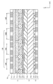
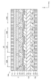
- FIG. 3 is a schematic cross-sectional view showing the configuration of the display panel 10.
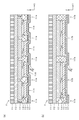
- FIG. 3 is a schematic cross-sectional view showing a configuration of an EL panel section 11 in the display panel 10, where (a) is a schematic cross-sectional view taken along A1-A2 in FIG. 2, and (b) is taken along B1-B2 in FIG.
- FIG. 3 is a schematic plan view showing a configuration of a CF panel section 12 in the display panel 10.
- FIG. 4A and 4B are schematic cross-sectional views showing the configuration of the CF panel section 12 in the display panel 10, wherein FIG. 4A is a schematic cross-sectional view taken along line C1-C2 in FIG. 4 and FIG. 4B is a cross-sectional view taken along line E1-E2 in FIG.
- FIG. (A) to (d) are schematic views showing the manufacturing process of the EL panel unit 11, wherein (a) shows a step of forming an insulating film and (b) shows a step of forming a metal thin film. , (C) shows the step of forming the anode and the auxiliary electrode, and (d) shows the step of forming the bank material layer.
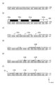
- (A) to (d) is a schematic diagram showing a manufacturing process of the EL panel unit 11, (a) shows a step of forming a bank, (b) shows a step of forming an organic light emitting layer, (C) shows the process of forming a cathode, (d) shows the process of forming a sealing layer.
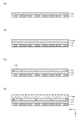
- (A) to (f) is a schematic diagram showing the manufacturing process of the CF panel unit 12, wherein (a) shows a step of forming a BM material layer, (b) shows a step of arranging a mask, (C) shows the step of forming the BM layer, (d) shows the step of forming the B-CF layer, (e) shows the step of forming the G-CF layer, and (f) shows the step of forming R-CF. The process of forming a layer is shown.
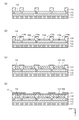
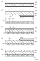
- (A) to (e) is a schematic diagram showing a process of attaching the EL panel unit 11 and the CF panel unit 12, and (a) shows a step of preparing a first non-flowable resin, (b) ) Shows a step of adhering the first non-flowable resin to the CF panel portion, (c) shows a state where the first non-flowable resin is in close contact with the main surface of the CF panel layer, and (d) ) Shows a step of exposing the main surface of the first non-flowable resin, and (e) shows a step of sticking the second non-flowable resin.
- FIG. 1 is a schematic diagram showing the process of attaching the EL panel unit 11 and the CF panel unit 12, wherein (a) shows the process of attaching the EL panel unit, and (b) A state where the second non-flowable resin is not attached to the EL panel portion is shown, and (c) shows a step of forming the first sealing resin layer and the second sealing resin layer.
- 6 is a schematic cross-sectional view showing a configuration of a display panel 10A according to Embodiment 2.
- FIG. 12 is a schematic cross-sectional view showing a configuration of a display panel 10B according to Embodiment 3.
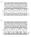
- (A) is a schematic cross-sectional view illustrating a configuration of a display panel according to a modification example in which the height of the CF layer is lower than the height of the BM layer
- (b) is a diagram illustrating the height of the CF layer of the BM layer. It is a schematic cross section which shows the structure of the display panel which concerns on a modification higher than height.
- the density of the resin between panel parts differs for every area
- Such a resin flow applies a shearing force to a film body (for example, in the case of an organic EL display panel, a sealing layer, an electrode layer, or an organic EL layer in the EL panel portion) existing on the opposite surface side of the panel portion.
- a shearing force increases to some extent, it is considered that film peeling occurs.
- Peeling of the film in the panel part directly leads to a decrease in display quality, and it is important to improve the display quality of the display panel to reduce the shearing force applied to the film body as much as possible when executing the bonding process. Become.
- the manufacturing method of the display panel which concerns on 1 aspect of this invention WHEREIN The process of preparing the 1st panel part in which the 1st main surface which is one main surface has uneven
- the first panel portion By arranging the first panel portion so that the main surface is in contact with the first and second non-flowable resins by heating or irradiating them to impart fluidity to the resins, and then curing them. , Forming first and second sealing resin layers from the first and second non-flowable resins, respectively. And before the heating or light irradiation in the step of forming the first and second sealing resin layers, the viscosity of the second non-flowable resin is the first non-flowable resin. Lower than the viscosity of
- positioning the said 1st panel part are both under pressure reduction atmosphere.
- the second non-flowable resin includes the top portion of the convex portion and the bottom portion of the concave portion in the concavo-convex shape of the first main surface of the first panel portion.
- the first non-flowable resin is in contact with the entire second main surface of the second panel portion.
- a difference between the viscosity of the first non-flowable resin and the viscosity of the second non-flowable resin is 1000 Pa ⁇ s or more.
- the viscosity of the first non-flowable resin is 35000 Pa ⁇ s or less, and the viscosity of the second non-flowable resin is 15000 Pa. -It is more than s.
- the first panel unit includes a substrate and a light emitting region and a non-light emitting region that are located on the substrate and are adjacent to each other in plan view.
- the concave portion in the concavo-convex shape of the first main surface corresponds to the light emitting region
- the convex portion in the concavo-convex shape of the first main surface corresponds to the non-light emitting region.
- the second main surface of the second panel portion is flatter than the first main surface of the first panel portion.
- the manufacturing method of the display panel which concerns on 1 aspect of this invention WHEREIN The process of preparing the 1st panel part in which the 1st main surface which is one main surface has uneven
- the first, second and third non-flowable resins are heated or irradiated with light to make the resin flowable.
- a difference between the viscosity of the third non-flowable resin and the viscosity of the first non-flowable resin is 1000 Pa ⁇ s or more.
- the viscosity of the third non-flowable resin is 35000 Pa ⁇ s or more.
- the display panel includes a substrate, and a light emitting region and a non-light emitting region that are located on the substrate and are adjacent to each other in plan view.
- a concave portion in the uneven shape of the surface corresponds to the light emitting region, and a convex portion in the uneven shape of the first main surface corresponds to the non-light emitting region.
- the first main surface which is one main surface has an uneven shape, and the first main surface of the first panel portion is spaced from each other. It arrange
- the top part of a convex part is a said 1st panel part rather than the bottom part of a recessed part. And has a concavo-convex shape projecting to the side, and is disposed between the second sealing resin layer and the first panel portion, and one main surface of the second sealing resin layer is the second sealing resin layer.
- the display panel includes a substrate, and a light emitting region and a non-light emitting region that are located on the substrate and are adjacent to each other in plan view.
- a concave portion in the concavo-convex shape of the surface corresponds to a light emitting region
- a convex portion in the concavo-convex shape of the first main surface corresponds to a non-light emitting region.
- the non-light emission of the first panel unit in the second panel unit when the first panel unit and the second panel unit are viewed in plan, the non-light emission of the first panel unit in the second panel unit.
- a region corresponding to the region is a non-light emission corresponding region
- the concave portion of the second main surface of the second panel portion is provided in the non-light emission corresponding region.
- the non-light emission of the first panel unit in the second panel unit when the first panel unit and the second panel unit are viewed in plan, the non-light emission of the first panel unit in the second panel unit.
- a region corresponding to the region is a non-light emission corresponding region
- the convex portion of the second main surface in the second panel portion is provided in the non-light emission corresponding region.
- the second panel portion is formed adjacent to the substrate, a color filter layer formed on the substrate, and the color filter layer.
- the display device 1 includes an organic EL display panel (hereinafter simply referred to as “display panel”) 10 and a drive / control unit 20 connected thereto.
- the display panel 10 is a panel using an electroluminescence phenomenon of an organic material and has a plurality of pixel portions.
- the display panel 10 includes a plurality of subpixels 100R, 100G, and 100B that are two-dimensionally arranged in the XY direction.
- One pixel 100 is configured by the sub-pixels 100R, 100G, and 100B arranged adjacent to each other.
- the drive / control unit 20 includes four drive circuits 21 to 24 and a control circuit 25.
- the arrangement relationship between the display panel 10 and the drive / control unit 20 in the display device 1 is not limited to the form shown in FIG. Further, the circuit included in the drive / control unit 20 is not limited to the form shown in FIG.
- the pixel configuration is not limited to the form composed of R, G, and B sub-pixels as shown in FIG. 2, and one pixel may be configured from four or more colors.
- an EL panel unit 11 in which a plurality of film bodies 111 to 117 are stacked on a substrate 111, and a color filter (CF) in which layers 122 and 123 are stacked on a substrate 121.
- the panel portion 12 is disposed so as to face the sealing resin layer 13 therebetween.
- the sealing resin layer 13 is on both the Z-axis direction lower main surface (first main surface) in the EL panel unit 11 and the Z-axis direction upper main surface (second main surface) in the CF panel unit 12. It touches.
- the sealing resin layer 13 plays a role of suppressing entry of moisture, air, and the like from the outside into the EL panel unit 11 in addition to the role of joining the EL panel unit 11 and the CF panel unit 12.
- the EL panel unit 11 has an interlayer insulating film on one main surface (the main surface on the lower side in the Z-axis direction) of the substrate 111. 112 are stacked.
- the substrate 111 has a TFT layer (not shown).
- the interlayer insulating film 112 also has a role of electrical insulation and a role of a planarizing film for suppressing the influence of unevenness on the surface of the substrate 111 due to the TFT layer.
- anodes 113 are formed in units of subpixels 100R, 100G, and 100B. As shown in FIGS. 4A and 4B, the anode 113 has a shape that is longer in the Y-axis direction than in the X-axis direction.
- a bank 114 is provided between adjacent anodes 113.
- the bank 114 is provided to surround the periphery of the bank 113 so as to overlap with a part of the anode 113, and defines a concave portion of a portion to be the subpixels 100R, 110G, and 100B.
- the bank 114 has a sectional shape in which the side surface of the bank 114 rises vertically, but this is for convenience and may actually be a slope. That is, the bank 114 may have a trapezoidal cross-sectional shape.
- an organic light emitting layer 115 is laminated on the anode 113.
- the organic light emitting layer 115 is a layer that emits light in a wavelength region corresponding to each of the subpixels 100R, 100G, and 100B.
- the configuration in which the anode 113 and the organic light emitting layer 115 are in contact with each other is employed as an example, but a configuration in which a hole injection layer, a hole transport layer, or the like is interposed between layers is employed. You can also.
- a cathode 116 and a sealing layer 117 are sequentially laminated.
- the cathode 116 and the sealing layer 117 are formed in a continuous state over the entire EL panel unit 11, and are also formed on the tops of the banks 114.
- a portion corresponding to the top of the bank 114 becomes a convex portion 117 a downward in the Z-axis direction.
- the portion corresponding to is a concave portion 117b that is recessed upward in the Z-axis direction, and has a concave-convex shape as a whole.
- the uneven gap G e1 exists on the lower main surface in the Z-axis direction of the EL panel unit 11.
- the configuration in which the organic light emitting layer 115 and the cathode 116 are in contact with each other is employed as an example.
- a configuration in which an electron injection layer, an electron transport layer, or the like is interposed between layers is employed.
- the EL panel unit 11 includes the substrate 111 and the light emitting region and the non-light emitting region that are located on the substrate 111 and are adjacent to each other in plan view, and the light emitting region is concave with respect to the non-light emitting region.
- the shape of the first main surface which is one main surface of the EL panel unit 11 reflects the uneven shape formed by the light emitting region and the non-light emitting region.
- the CF panel unit 12 has a red color filter layer (R-CF layer) 122R, a green color filter layer.
- R-CF layer red color filter layer
- a (G-CF layer) 122G and a blue color filter layer (B-CF layer) 122B are two-dimensionally arranged in the XY direction.
- the arrangement of the color filter layers 122R, 122G, and 122B corresponds to the subpixels 100R, 100G, and 100B (see FIG. 2).
- planar shapes of the color filter layers 122R, 122G, and 122B also have a rectangular shape that has a longer Y-axis direction than the X-axis direction, corresponding to the subpixels 100R, 100G, and 100B.
- BM layer black matrix layer
- CF layers color filter layers
- the BM layer 123 is a black layer provided for the purpose of improving the display contrast by suppressing the reflection of light emission on the display surface of the display panel 10 and the incidence of external light. As shown in FIG. 3, the BM layer 123 in the CF panel unit 12 is formed in a state corresponding to (opposed to) the bank 114 in the EL panel unit 11.
- the height (thickness) up to the upper surface 123 a of the BM layer 123 with respect to the surface of the substrate 121 is the upper surface of the CF layer 112. It is the same as the height (thickness) up to 122a. That is, the Z-axis direction upper principal surface of the CF panel portion 12 is flatter than the Z-axis direction lower principal surface of the EL panel portion 11.
- Substrate 111,121 examples include a glass substrate, a quartz substrate, a silicon substrate, molybdenum sulfide, copper, zinc, aluminum, stainless steel, magnesium, iron, nickel, gold, silver, and other metal substrates, a gallium arsenide group, and the like.
- a semiconductor substrate, a plastic substrate, or the like can be used.
- thermoplastic resin such as polyethylene, polypropylene, ethylene-propylene copolymer, ethylene-vinyl acetate copolymer (EVA), cyclic polyolefin, modified polyolefin, polyvinyl chloride, polyvinylidene chloride, polystyrene, polyamide, polyimide (PI), Polyamideimide, polycarbonate, poly- (4-methylbenten-1), ionomer, acrylic resin, polymethyl methacrylate, acrylic-styrene copolymer (AS resin), butadiene-styrene copolymer, polio copolymer (EVOH) ), Polyesters such as polyethylene terephthalate (PET), polybutylene terephthalate, polyethylene naphthalate (PEN), precyclohexane terephthalate (PCT), polyethers, polyether ketones Polyethers
- a known TFT layer is formed on the substrate 111 in the EL panel unit 11.
- illustration is abbreviate
- the interlayer insulating film 112 is formed using an organic compound such as polyimide, polyamide, or acrylic resin material.
- the interlayer insulating film 112 preferably has organic solvent resistance.
- the interlayer insulating film 112 may be subjected to an etching process, a bake process, or the like during the manufacturing process, a material having high resistance that does not excessively deform or deteriorate the process is used. It is desirable to be formed.
- Anode 113 is made of a metal material containing silver (Ag) or aluminum (Al).
- the surface portion thereof preferably has high reflectivity.
- the anode 113 not only a single layer structure made of a metal material as described above but also a laminate of a metal layer and a transparent conductive layer can be adopted.
- a constituent material of the transparent conductive layer for example, indium tin oxide (ITO), indium zinc oxide (IZO), or the like can be used.
- the bank 114 is formed using an organic material such as a resin and has an insulating property.
- organic material used for forming the bank 114 include acrylic resin, polyimide resin, and novolac type phenol resin.
- the bank 114 can be subjected to fluorine treatment on the surface in order to give the surface water repellency.
- the structure of the bank 114 not only a single layer structure as shown in FIG. 3 and FIGS. 4A and 4B but also a multilayer structure of two or more layers can be adopted.
- the above materials can be combined for each layer, and an inorganic material and an organic material can be used for each layer.
- Organic light emitting layer 115 As described above, the organic light emitting layer 115 has a function of emitting light by generating an excited state by injecting and recombining holes and electrons. As a material used for forming the organic light emitting layer 115, it is necessary to use a light emitting organic material that can be formed by a wet printing method.
- the oxinoid compound, perylene compound, coumarin compound, azacoumarin compound, oxazole compound, oxadiazole compound, perinone compound, pyrrolopyrrole described in the patent publication (Japan / JP-A-5-163488) Compound, naphthalene compound, anthracene compound, fluorene compound, fluoranthene compound, tetracene compound, pyrene compound, coronene compound, quinolone compound and azaquinolone compound, pyrazoline derivative and pyrazolone derivative, rhodamine compound, chrysene compound, phenanthrene compound, cyclopentadiene compound, stilbene compound , Diphenylquinone compound, styryl compound, butadiene compound, dicyanomethylenepyran compound, dicyanomethylenethiopyran compound, fluoro Cein compounds, pyrylium compounds, thiapyrylium
- the cathode 116 is formed using, for example, indium tin oxide (ITO) or indium zinc oxide (IZO).
- ITO indium tin oxide
- IZO indium zinc oxide
- the transmittance is 80 [[%]] or more.
- the sealing layer 117 has a function of suppressing exposure of an organic layer such as the organic light emitting layer 115 to moisture or exposure to air.
- an organic layer such as the organic light emitting layer 115
- silicon nitride (SiN) silicon oxynitride (SiON) It is formed using materials such as.
- a sealing resin layer made of a resin material such as an acrylic resin or a silicone resin may be provided over a layer formed using a material such as silicon nitride (SiN) or silicon oxynitride (SiON).
- the sealing layer 117 needs to be formed of a light-transmitting material.
- the CF layer 122 in the CF panel unit 12 is made of a known material that selectively transmits visible light in the wavelength ranges of red (R), green (G), and blue (B). For example, it is formed based on an acrylic resin.
- the BM layer 123 in the CF panel unit 12 is made of, for example, an ultraviolet curable resin material containing a black pigment having excellent light absorption and light shielding properties.
- an ultraviolet curable resin material include an acrylic resin.
- the sealing resin layer 13 is made of various transparent resin materials. Specifically, it is composed of, for example, an epoxy resin, a silicone resin, or the like.
- the hole injection layer is formed by oxidizing, for example, silver (Ag), molybdenum (Mo), chromium (Cr), vanadium (V), tungsten (W), nickel (Ni), iridium (Ir), etc. Or a layer made of a conductive polymer material such as PEDOT (a mixture of polythiophene and polystyrene sulfonic acid).
- a metal oxide is used as the constituent material of the hole injection layer
- the organic light emitting layer is formed more stably than the case where a conductive polymer material such as PEDOT is used or the generation of holes is assisted. It has a function of injecting holes into 108 and has a large work function.
- the hole injection layer is composed of an oxide of a transition metal
- a plurality of levels can be taken by taking a plurality of oxidation numbers.
- the hole injection becomes easy and the drive voltage is reduced. Can be reduced.
- the hole transport layer is formed using a polymer compound that does not have a hydrophilic group.
- a polymer compound that does not have a hydrophilic group for example, polyfluorene or a derivative thereof, or a polymer compound such as polyarylamine or a derivative thereof that does not have a hydrophilic group can be used.
- an electron transport layer is interposed between the organic light emitting layer 115 and the cathode 116, for example, the following materials can be used.
- the electron transport layer has a function of transporting electrons injected from the cathode 116 to the organic light emitting layer 115, and includes, for example, an oxadiazole derivative (OXD), a triazole derivative (TAZ), and phenanthroline. Derivatives (BCP, Bphen) are used.
- the sealing resin layer 13 has a two-layer structure of a first sealing resin layer 13a and a second sealing resin layer 13b.
- the first sealing resin layer 13a is disposed between the EL panel unit 11 and the CF panel unit 12 and does not contact the lower main surface in the Z-axis direction of the EL panel unit 11, but the EL panel unit in the CF panel unit 12 11 is in contact with the Z-axis direction upper main surface opposite to the Z-axis direction lower main surface.
- the second sealing resin layer 13b is disposed between the EL panel portion 11 and the first sealing resin layer 13a and is in contact with at least the first sealing resin layer 13a. In the present embodiment, the second sealing resin layer 13b is in contact with both the first sealing resin layer 13a and the lower main surface in the Z-axis direction of the EL panel unit 11.
- the viscosity of the non-flowable resin that is the raw material of the second sealing resin layer 13b is lower than the viscosity of the non-flowable resin that is the raw material of the first sealing resin layer 13a.
- the non-flowable resin that is a raw material of the first sealing resin layer 13a is a first non-flowable resin 130 (see FIG. 10) described later, and the non-flowable resin that is a raw material of the second sealing resin layer 13b.
- the resin is a second non-flowable resin 132 (see FIG. 10) described later.
- the EL panel portion 11 and the CF panel portion 12 are used as the raw material for the second sealing resin layer 13b in contact with the main surface of the EL panel portion 11 having a larger unevenness on the main surface.
- the viscosity of the non-flowable resin is set lower than the viscosity of the non-flowable resin that is the raw material of the first sealing resin layer 13a.
- resin flow occurs when heat or light energy is applied to the resin material.
- the EL panel is formed by resin flow as compared with the case where the sealing resin layer 13 is composed only of a high-viscosity non-flowable resin.
- the shear force applied to each layer of the part 11 can be reduced. As a result, it is considered that film peeling is suppressed.
- the difference between the viscosity of the non-flowable resin that is the raw material of the first sealing resin layer 13a and the viscosity of the non-flowable resin that is the raw material of the second sealing resin layer 13b is not particularly limited. If the viscosity of the non-flowable resin that is the raw material of the second sealing resin layer 13b is lower than that of the first sealing resin layer 13a, the viscosity of the non-flowable resin that is the raw material of the second sealing resin layer 13b is The occurrence of film peeling is suppressed compared to the case where the first sealing resin layer 13a is the same.
- the difference between the viscosity of the non-flowable resin that is the raw material of the first sealing resin layer 13a and the viscosity of the non-flowable resin that is the raw material of the second sealing resin layer 13b is, for example, 1000 [Pa ⁇ s] or more. It is desirable.
- the viscosity of the non-flowable resin that is the raw material of the first sealing resin layer 13a is desirably 35000 [Pa ⁇ s] or less, and the viscosity of the non-flowable resin that is the raw material of the second sealing resin layer 13b is The viscosity is desirably 15000 [Pa ⁇ s] or more.
- the upper limit value of the film thickness of the first sealing resin layer 13a and the film thickness of the second sealing resin layer 13b are not particularly limited, but the lower limit value of the film thickness of the second sealing resin layer 13b is the EL panel part.
- 11 is desirably a film thickness that can fill the unevenness of the main surface on the lower side in the Z-axis direction. That is, it is desirable that the film thickness be equal to or greater than the uneven gap G e1 shown in FIG.
- Manufacturing Method A manufacturing method of the display panel 10 according to the present embodiment will be described with reference to FIGS.
- the manufacturing process of the display panel 10 according to the present embodiment includes (1) a process of preparing the EL panel unit 11, (2) a process of preparing the CF panel unit 12, and (3) an EL panel unit 11. And the process of bonding the CF panel portion 12 together will be described.
- Step of Preparing EL Panel Unit 11 As shown in FIG. 7A, an interlayer insulating film 112 is formed on a substrate 111 on which a TFT layer is formed. Then, as shown in FIG. 7B, a metal thin film 1130 is formed on the interlayer insulating film 112. The formation of the metal thin film 1130 can be performed using, for example, a sputtering method.
- the metal thin film 1130 on the interlayer insulating film 112 is patterned to form the anode 113 and the auxiliary electrode (bus bar) 118.
- the patterning can be performed using, for example, a photolithography method.
- a bank material layer 1140 made of an insulating organic material is formed so as to cover the anode 113 and the auxiliary electrode 118.
- the bank material layer 1140 is patterned so that the banks 114 are erected between the adjacent anodes 113 and between the adjacent anode 113 and the auxiliary electrode 118.
- the patterning for forming the bank 114 is performed, for example, by placing a mask having a predetermined opening on the upper side and performing exposure, and thereafter removing unnecessary portions (developing a wet process) by development. .
- the organic light emitting layers 115R, 115G, and 115B having different emission colors for each recess are formed in the recess 114a defined by the bank 114.
- the recess 114b above the auxiliary electrode 118 no organic light emitting layer is formed.
- the organic light emitting layers 115R, 115G, and 115B can be formed using, for example, an ink jet method. Specifically, an ink containing an organic light emitting material is applied to each of the recesses 114a and then dried. Can be done.
- the cathode 116 is continuously formed so as to cover the organic light emitting layer 115 (generically referring to the organic light emitting layers 115R, 115G, and 115B) and the exposed portion of the bank 114.
- the formation of the cathode 116 can be performed using, for example, a sputtering method.
- a sealing layer 117 is formed so as to cover the cathode 116.
- the formation of the sealing layer 117 can be performed using, for example, a sputtering method, a CVD (chemical vapor deposition) method, an ALD (atomic layer deposition) method, or the like.
- a BM material layer 1230 is laminated on one main surface of the substrate 121.
- a BM paste is prepared by dispersing a BM material mainly composed of an ultraviolet curable resin (for example, an ultraviolet curable acrylic resin) material and adding a black pigment to the solution. Then, the adjusted paste is applied so as to cover one main surface of the substrate 121.
- an ultraviolet curable resin for example, an ultraviolet curable acrylic resin
- the BM material layer 1230 is formed by drying the applied paste and volatilizing the solvent to some extent.
- a mask 500 is placed on the BM material layer 1230 that has been dried until the form can be maintained.
- a window portion 500a is formed in the bank 114 of the EL panel portion 11 so as to correspond to the formation position.
- the exposed surface of the BM material layer 1230 is irradiated with ultraviolet rays through the window portion 500a of the mask 500.
- the dried BM material layer 1230 is developed to remove the unexposed portion, and then baking is performed to form a BM layer 123 as shown in FIG. 9C. Can be formed.
- the formed BM layer 123 is disposed at a position corresponding to the bank 114 in the EL panel unit 11.
- a blue CF layer 122B is formed in the opening 123a defined by the BM layer 123.
- a CF material mainly composed of an ultraviolet curable resin component is dispersed in a solvent to prepare a paste, and then this paste is formed to volatilize the solvent to some extent.
- a mask having a predetermined window portion is disposed (not shown), and ultraviolet rays are irradiated through the window portion.
- a B-CF layer 122B as shown in FIG. 9D is formed. Note that, as described above, in the present embodiment, all the CF layers 122 are formed with their outer edge portions riding on the BM layer 123.
- the order of forming the R-CF layer 122R, the G-CF layer 122G, and the B-CF layer 122B may be other than the above.
- Step of bonding EL panel portion 11 and CF panel portion 12 (i) As shown in FIG. 10A, a sheet-like first non-flowable resin (material) 130 is prepared. Laminate films 131 a and 131 b are attached to both main surfaces of the first non-flowable resin 130.
- one laminate film 131a attached to the first non-flowable resin 130 is peeled off, and the exposed main surface 130a is attached to the CF panel portion 12. .
- the bonding of the first non-flowable resin 130 and the CF panel unit 12 is performed in a reduced pressure atmosphere.
- the main surface 130 a of the first non-flowable resin 130 is the upper surface 123 a of the BM layer 123 and the upper surface 122 a of the CF layer 122 in the CF panel portion 12 after being stuck. Is in close contact with the entire main surface including
- the EL panel unit 11 is attached to the main surface 132 a of the second non-flowable resin 132. This step is also performed under a reduced pressure atmosphere. Therefore, as shown in FIG. 11 (b), the main surface 132a of the second non-fluid resin 132 is attached to the bottom of the concave portion 117b and the convex portion 117a of the sealing layer 117 in the EL panel portion 11 after being stuck. It has been in close contact with the entire main surface including the top.
- the viscosity of the second non-flowable resin 132 is lower than the viscosity of the first non-flowable resin 130, when the fluidity is imparted to the resin in (iv) above, the EL The shear force applied to each layer of the panel unit 11 can be reduced. As a result, occurrence of film peeling due to this shear force can be suppressed.
- Embodiment 2 A schematic configuration of the display panel 10A according to Embodiment 2 will be described with reference to FIG. The difference from the display panel 10 according to the first embodiment is the configuration of the CF panel portion 12A and the sealing resin layer 13A.
- the upper surface of the CF layer 124 is formed to be higher than the upper surface of the BM layer 123, not only the main surface of the EL panel unit 11 but also the upper main surface in the Z-axis direction of the CF panel unit 12A
- the top part of the convex part protrudes to the EL panel part 11 side rather than the bottom part of the concave part, and has an uneven shape as a whole.
- the sealing resin layer 13A has a three-layer structure, and includes a first sealing resin layer 13c, a second sealing resin layer 13d, and a third sealing resin layer 13e.
- the first sealing resin layer 13c has a sheet shape, is disposed between the EL panel unit 11 and the CF panel unit 12A, and does not contact the lower main surface in the Z-axis direction of the EL panel unit 11, but the CF panel unit 12A is in contact with the upper main surface in the Z-axis direction.
- the second sealing resin layer 13d has a sheet shape, is disposed between the first sealing resin layer 13c and the EL panel unit 11, and is in contact with at least the first sealing resin layer 13c.
- the second sealing resin layer 13d is in contact with the first sealing resin layer 13c, but is not in contact with the lower main surface in the Z-axis direction of the EL panel unit 11.
- the third sealing resin layer 13e has a sheet shape, is disposed between the second sealing resin layer 13d and the EL panel unit 11, and is below the second sealing resin layer 13d and the EL panel unit 11 in the Z-axis direction. It touches both sides. And the viscosity of the raw material of the 1st sealing resin layer 13c and the raw material of the 3rd sealing resin layer 13e is lower than the viscosity of the raw material of the 2nd sealing resin layer 13d.
- the non-flowable resin that is the raw material of the first sealing resin layer 13c is the first non-flowable resin
- the non-flowable resin that is the raw material of the second sealing resin layer 13d is the second non-flowable resin.
- the non-flowable resin that is a resin and is the raw material of the third sealing resin layer 13e is the third non-flowable resin.
- the convex part of the Z-axis direction upper principal surface (second principal surface) in the CF panel portion 12A may be provided in the non-light emission corresponding region.
- the difference between the viscosity of the third non-flowable resin and the viscosity of the first non-flowable resin is preferably 1000 Pa ⁇ s or more.
- the viscosity of the third non-flowable resin is preferably 15000 Pa ⁇ s or more. Also in this case, the occurrence of film peeling due to the shear force can be suppressed.
- Embodiment 3 A schematic configuration of the display panel 10B according to Embodiment 3 will be described with reference to FIG.
- the EL panel unit 11A, the CF panel unit 12A, and the sealing resin layer 13B are all different from the display panel 10 according to the first embodiment.
- the sealing layer 1171 in the EL panel portion 11A is different from the first embodiment, and since the surface thereof is formed flat, the lower main surface in the Z-axis direction of the EL panel portion 11A is flat.
- the CF panel portion 12A has the same configuration as that of the second embodiment, and the upper main surface in the Z-axis direction has an uneven shape.
- the sealing resin layer 13B has a two-layer structure of a first sealing resin layer 13f and a second sealing resin layer 13g.
- the first sealing resin layer 13f is disposed between the EL panel unit 11A and the CF panel unit 12A and does not contact the lower main surface of the EL panel unit 11A in the Z-axis direction, but the Z-axis direction of the CF panel unit 12A. It is in contact with the upper main surface.
- the second sealing resin layer 13g is disposed between the EL panel portion 11A and the first sealing resin layer 13f, and both the first sealing resin layer 13f and the lower main surface in the Z-axis direction of the EL panel portion 11A. Is in contact with The viscosity of the raw material of the first sealing resin layer 13f is lower than the viscosity of the raw material of the second sealing resin layer 13g.
- the CF panel portion 342 in the CF panel portion 34 has a lower height than the BM layer 343 and is in contact with the sealing resin layer 35.
- the main surface of 34 has an uneven shape as a whole.
- the height of the CF panel portion 36 with the CF layer 362 is higher than the height of the BM layer 363 and is in contact with the sealing resin layer 37.
- the main surface of the CF panel portion 36 has an uneven shape as a whole.
- a so-called top emission structure organic EL display panel is used as an example.
- the present invention is not limited to this, and the above configuration can also be adopted for a bottom emission structure organic EL display device. it can.
- one of the two panel portions is a CF panel portion.
- the CF panel portion formed with a color filter layer is not necessarily required.
- a substrate made of glass or resin may be used.
- a configuration in which a plurality of light emitting regions (subpixels) are arranged in a matrix shape in a plan view is employed. It is not limited to this. For example, it is possible to adopt an arrangement form of a honeycomb structure.
- one embodiment of the present invention is applied to a pixel bank that surrounds the periphery of each sub-pixel by banks formed in a grid pattern (lattice shape) is described, but the present invention is not limited to this.
- One embodiment of the present invention can also be applied to a line bank that partitions each subpixel in a stripe shape.
- fluidity liquidity was provided by irradiating light (for example, ultraviolet light) with respect to non-flowable resin
- irradiating light for example, ultraviolet light
- Fluidity can be imparted by heating.
- the step of bonding the EL panel part and the CF panel part through the non-flowable resin does not necessarily have to be performed in a reduced pressure atmosphere.
- a force is applied between the EL panel unit and the CF panel unit, and between the EL panel unit and the non-flowable resin, and between the CF panel unit and the non-flowing. It is good also as eliminating the space
- the present invention can be applied not only to the organic EL display panel but also to various display panels, and the same effect can be obtained in that case.
- the present invention is useful when realizing a display panel having high display quality.
Landscapes
- Engineering & Computer Science (AREA)
- Manufacturing & Machinery (AREA)
- Microelectronics & Electronic Packaging (AREA)
- Electroluminescent Light Sources (AREA)
- Optical Filters (AREA)
Abstract
Description
上述の非流動性樹脂を用いたパネル部同士の接合は、次のような工程を経てなされる。
(工程a) 一方のパネル部(例えば、第2パネル部)に非流動性樹脂を形成する。
(工程b) 非流動性樹脂の残りの主面に、もう一方のパネル部(例えば、第1パネル部)を貼着する。
(工程c) 非流動性樹脂に対して、加熱もしくは光照射を行うことで流動性を付与した後、硬化させることにより、パネル部同士の貼り合わせが完了する。
本発明の一態様に係る表示パネルの製造方法は、一方の主面である第1主面が凹凸形状を有する第1パネル部を準備する工程と、第2パネル部を準備する工程と、前記第2パネル部における一方の主面である第2主面に、一方の主面が接するようにシート状の第1非流動性樹脂を配置する工程と、前記第1非流動性樹脂の他方の主面に、一方の主面が接するようにシート状の第2非流動性樹脂を配置する工程と、前記第2非流動性樹脂の他方の主面に、前記第1パネル部の前記第1主面が接するように前記第1パネル部を配置する工程と、前記第1および第2非流動性樹脂に対して加熱もしくは光照射を行って樹脂に流動性を付与した後、硬化させることにより、前記第1および第2非流動性樹脂からそれぞれ第1および第2封止樹脂層を形成する工程と、を備え、前記第1および第2封止樹脂層を形成する工程で前記加熱もしくは光照射を行う前において、前記第2非流動性樹脂の粘度は、前記第1非流動性樹脂の粘度よりも低い。
1.表示装置の概略構成
本発明の実施の形態に係る表示装置1の概略構成について、図1および図2を用い説明する。
表示パネル10の構成について、図3から図6を用い説明する。なお、ここでは、第1パネル部としてELパネル部を用い、第2パネル部としてCFパネル部を用いて説明する。
図4(a)、(b)に示すように、ELパネル部11は、基板111の一方の主面(Z軸方向下側の主面)に層間絶縁膜112が積層されている。基板111は、TFT層を有するものである(図示を省略。)。層間絶縁膜112は、電気的な絶縁の役割と、TFT層による基板111表面の凹凸の影響を抑制するための平坦化膜としての役割も担っている。
以上の構成により、ELパネル部11は、基板111と、基板111上に位置し平面視において互いに隣接する発光領域および非発光領域とを有し、発光領域は非発光領域に対して凹となるように配置される。また、ELパネル部11の一方の主面である第1主面の形状には、発光領域と非発光領域とがなす凹凸形状が反映されている。
図5に示すように、X-Y方向での平面視において、CFパネル部12では、赤色のカラーフィルタ層(R-CF層)122R、緑色のカラーフィルタ層(G-CF層)122G、青色のカラーフィルタ層(B-CF層)122BがX-Y方向に二次元配置されている。各カラーフィルタ層122R,122G,122Bの配置は、サブピクセル100R,100G,100Bに対応している(図2を参照)。そして、各カラーフィルタ層122R、122G、122Bの平面形状も、サブピクセル100R,100G,100Bに対応して、X軸方向に比べてY軸方向が長い矩形状となっている。
(1)基板111,121
基板111,121の構成材料としては、例えば、ガラス基板、石英基板、シリコン基板、硫化モリブデン、銅、亜鉛、アルミニウム、ステンレス、マグネシウム、鉄、ニッケル、金、銀などの金属基板、ガリウム砒素基などの半導体基板、プラスチック基板等を採用することができる。
層間絶縁膜112は、例えば、ポリイミド、ポリアミド、アクリル系樹脂材料などの有機化合物を用い形成されている。ここで、層間絶縁膜112は、有機溶剤耐性を有することが好ましい。また、層間絶縁膜112は、製造工程中において、エッチング処理、ベーク処理等が施されることがあるので、それらの処理に対して過度に変形や変質などを生じない高い耐性を有する材料を用い形成されることが望ましい。
アノード113は、銀(Ag)またはアルミニウム(Al)を含む金属材料から構成されている。トップエミッション型の本実施の形態に係る表示パネル10の場合には、その表面部が高い反射性を有することが好ましい。
バンク114は、樹脂等の有機材料を用い形成されており絶縁性を有する。バンク114の形成に用いる有機材料の例としては、アクリル系樹脂、ポリイミド系樹脂、ノボラック型フェノール樹脂等があげられる。バンク114は、表面に撥水性をもたせるために、表面をフッ素処理することもできる。
有機発光層115は、上述のように、ホールと電子とが注入され再結合されることにより励起状態が生成され発光する機能を有する。有機発光層115の形成に用いる材料は、湿式印刷法を用い製膜できる発光性の有機材料を用いることが必要である。
カソード116は、例えば、酸化インジウムスズ(ITO)若しくは酸化インジウム亜鉛(IZO)などを用い形成される。本実施の形態のように、トップエミッション型の本実施の形態に係る表示パネル10の場合においては、光透過性の材料で形成されることが必要となる。光透過性については、透過率が80[[%]]以上とすることが好ましい。
封止層117は、有機発光層115などの有機層が水分に晒されたり、空気に晒されたりすることを抑制する機能を有し、例えば、窒化シリコン(SiN)、酸窒化シリコン(SiON)などの材料を用い形成される。また、窒化シリコン(SiN)、酸窒化シリコン(SiON)などの材料を用い形成された層の上に、アクリル樹脂、シリコーン樹脂などの樹脂材料からなる封止樹脂層を設けてもよい。
CFパネル部12におけるCF層122は、赤色(R)、緑色(G)、青色(B)の各色の波長域の可視光を選択的に透過する、公知の材料から構成される。例えば、アクリル樹脂をベースに形成されている。
CFパネル部12におけるBM層123は、例えば、光吸収性および遮光性に優れる黒色顔料を含む紫外線硬化樹脂材料から構成されている。具体的な紫外線硬化樹脂材料としては、例えば、アクリル樹脂等がある。
封止樹脂層13は、各種透明樹脂材料で構成されている。具体的には、例えば、エポキシ系樹脂、シリコーン系樹脂等から構成されている。
本実施の形態では省略しているが、アノード113と有機発光層115との間に、ホール注入層およびホール輸送層を介挿させる場合には、例えば、次のような材料を用いることができる。
ホール注入層は、例えば、銀(Ag)、モリブデン(Mo)、クロム(Cr)、バナジウム(V)、タングステン(W)、ニッケル(Ni)、イリジウム(Ir)などの酸化物、あるいは、PEDOT(ポリチオフェンとポリスチレンスルホン酸との混合物)などの導電性ポリマー材料からなる層である。なお、ホール注入層の構成材料として金属酸化物を用いる場合には、PEDOTなどの導電性ポリマー材料を用いる場合に比べて、ホールを安定的に、またはホールの生成を補助して、有機発光層108に対しホールを注入する機能を有し、大きな仕事関数を有する。
ホール輸送層は、親水基を備えない高分子化合物を用い形成されている。例えば、ポリフルオレンやその誘導体、あるいはポリアリールアミンやその誘導体などの高分子化合物であって、親水基を備えないものなどを用いることができる。
電子輸送層は、カソード116から注入された電子を有機発光層115へ輸送する機能を有し、例えば、オキサジアゾール誘導体(OXD)、トリアゾール誘導体(TAZ)、フェナンスロリン誘導体(BCP、Bphen)などを用い形成されている。
図3に示すように、本実施の形態に係る封止樹脂層13は、第1封止樹脂層13aと第2封止樹脂層13bの二層構造である。第1封止樹脂層13aは、ELパネル部11とCFパネル部12との間に配置され、ELパネル部11におけるZ軸方向下側主面と接しないが、CFパネル部12におけるELパネル部11のZ軸方向下側主面に対向するZ軸方向上側主面とは接する。第2封止樹脂層13bは、ELパネル部11と第1封止樹脂層13aとの間に配置され、少なくとも第1封止樹脂層13aと接する。本実施の形態においては、第2封止樹脂層13bは、第1封止樹脂層13aとELパネル部11のZ軸方向下側主面の双方に接している。
第2封止樹脂層13bの原料となる非流動性樹脂の粘度を、第1封止樹脂層13aの原料となる非流動性樹脂の粘度よりも低くすることにより、膜剥がれの発生が抑制される。これより、本実施の形態に係る表示パネル10では、高い表示品質を得ることができる。
本実施の形態に係る表示パネル10の製造方法について、図7から図11を用い説明する。なお、以下では、本実施の形態に係る表示パネル10の製造過程を、(1)ELパネル部11を準備する工程、(2)CFパネル部12を準備する工程、(3)ELパネル部11とCFパネル部12とを貼り合わせる工程に大きく分けて説明する。
(i) 図7(a)に示すように、TFT層が形成されてなる基板111上に、層間絶縁膜112を積層形成する。そして、図7(b)に示すように、層間絶縁膜112上に金属薄膜1130を形成する。金属薄膜1130の形成は、例えば、スパッタリング法を用い実行することができる。
(i) 図9(a)に示すように、基板121の一方の主面上に対し、BM材料層1230を積層形成する。BM材料層1230の形成では、先ず、紫外線硬化樹脂(例えば、紫外線硬化アクリル樹脂)材料を主成分とし、これに黒色顔料が添加されてなるBM材料を溶液に分散させてBMペーストを調整する。そして、調整されたペーストを基板121の一方の主面上を覆うように塗布する。
(i) 図10(a)に示すように、シート状の第1非流動性樹脂(材料)130を準備する。第1非流動性樹脂130の両主面には、ラミネートフィルム131a,131bが貼着されている。
実施の形態2に係る表示パネル10Aの概略構成について、図12を用い説明する。
実施の形態1に係る表示パネル10との相違点は、CFパネル部12Aおよび封止樹脂層13Aの構成である。
また、ELパネル部11およびCFパネル部12Aを平面視する場合に、CFパネル部12AにおけるELパネル部11の非発光領域に対応する領域を非発光対応領域とする。このとき、CFパネル部12AにおけるZ軸方向上側主面(第2主面)の凹部は、非発光対応領域内に設けられている。
実施の形態3に係る表示パネル10Bの概略構成について、図13を用い説明する。実施の形態1に係る表示パネル10に対し、ELパネル部11A、CFパネル部12Aおよび封止樹脂層13B全ての構成が異なる。
図14(a)に示す変形例では、CFパネル部34におけるCF層342の高さがBM層343の高さに比べて低くなっており、封止樹脂層35に接することになるCFパネル部34の主面は、全体として凹凸形状となっている。さらに、図14(b)に示す変形例では、CFパネル部36におけるCF層362との高さがBM層363の高さに比べて高くなっており、封止樹脂層37に接することになるCFパネル部36の主面は、全体として凹凸形状となっている。
上記実施の形態などでは、所謂、トップエミッション構造の有機EL表示パネルを一例として採用したが、本発明はこれに限定されず、ボトムエミッション構造の有機EL表示装置についても上記構成を採用することができる。
10,10A,10B 表示パネル
11 ELパネル部
12,34,36 CFパネル部
13,13A,13B,35,37 封止樹脂層
13a,13c 第1封止樹脂層
13b,13d 第2封止樹脂層
13e 第3封止樹脂層
13f 第1封止樹脂層
13g 第2封止樹脂層
20 駆動制御部
21~24 駆動回路
25 制御回路
100 ピクセル
100R Rサブピクセル
100G Gサブピクセル
100B Bサブピクセル
111 TFT基板
112 層間絶縁膜
113 アノード
114 バンク
115 有機発光層
115R R有機発光層
115G G有機発光層
115B B有機発光層
116 カソード
117 封止層
121 基板
122,342,362 カラーフィルタ層
122R Rカラーフィルタ層
122G Gカラーフィルタ層
122B Bカラーフィルタ層
123,343,363 ブラックマトリクス層
130 第1非流動性樹脂
132 第2非流動性樹脂
131a,131b ラミネートシート
500 マスク
1130 金属薄膜
1140 バンク材料層
1230 BM材料層
Claims (16)
- 一方の主面である第1主面が凹凸形状を有する第1パネル部を準備する工程と、
第2パネル部を準備する工程と、
前記第2パネル部における一方の主面である第2主面に、一方の主面が接するようにシート状の第1非流動性樹脂を配置する工程と、
前記第1非流動性樹脂の他方の主面に、一方の主面が接するようにシート状の第2非流動性樹脂を配置する工程と、
前記第2非流動性樹脂の他方の主面に、前記第1パネル部の前記第1主面が接するように前記第1パネル部を配置する工程と、
前記第1および第2非流動性樹脂に対して加熱もしくは光照射を行って樹脂に流動性を付与した後、硬化させることにより、前記第1および第2非流動性樹脂からそれぞれ第1および第2封止樹脂層を形成する工程と、を備え、
前記第1および第2封止樹脂層を形成する工程で前記加熱もしくは光照射を行う前において、前記第2非流動性樹脂の粘度は、前記第1非流動性樹脂の粘度よりも低い、
表示パネルの製造方法。 - 前記第1非流動性樹脂を配置する工程と、前記第1パネル部を配置する工程とは、ともに減圧雰囲気下で実行され、
当該両工程を実行した後において、
前記第2非流動性樹脂は、前記第1パネル部の前記第1主面の凹凸形状における凸部の頂部および凹部の底部を含む前記第1主面の全体に接しており、
前記第1非流動性樹脂は、前記第2パネル部の前記第2主面の全体に接している、
請求項1に記載の表示パネルの製造方法。 - 前記第1非流動性樹脂の粘度と前記第2非流動性樹脂の粘度との差が1000Pa・s以上である、
請求項1に記載の表示パネルの製造方法。 - 前記第1非流動性樹脂の粘度は、35000Pa・s以下であり、
前記第2非流動性樹脂の粘度は、15000Pa・s以上である、
請求項1に記載の表示パネルの製造方法。 - 前記第1パネル部は、基板と、当該基板上に位置し平面視において互いに隣接する発光領域および非発光領域とを有し、
前記第1主面の凹凸形状における凹部が前記発光領域に相当し、前記第1主面の凹凸形状における凸部が前記非発光領域に相当する、
請求項1に記載の表示パネルの製造方法。 - 前記第2パネル部の前記第2主面は、前記第1パネル部の前記第1主面よりも平坦である、
請求項1に記載の表示パネルの製造方法。 - 一方の主面である第1主面が凹凸形状を有する第1パネル部を準備する工程と、
第2パネル部を準備する工程と、
前記第2パネル部における一方の主面である第2主面に、一方の主面が接するようにシート状の第1非流動性樹脂を配置する工程と、
前記第1非流動性樹脂の他方の主面に、一方の主面が接するようにシート状の第2非流動性樹脂を配置する工程と、
前記第2非流動性樹脂の他方の主面に、一方の主面が接するようにシート状の第3非流動性樹脂を配置する工程と、
前記第3非流動性樹脂の他方の主面に、前記第1主面が接するように前記第1パネル部を配置する工程と、
前記第1、第2および第3非流動性樹脂に対して加熱もしくは光照射を行って樹脂に流動性を付与した後、硬化させることにより、前記第1、第2および第3非流動性樹脂からそれぞれ第1、第2および第3封止樹脂層を形成する工程と、を備え、
前記第1、第2および第3封止樹脂層を形成する工程で前記加熱もしくは光照射を行う前において、前記第2非流動性樹脂の粘度は、前記第1非流動性樹脂および前記第3非流動性樹脂の粘度よりも高い、
表示パネルの製造方法。 - 前記第2非流動性樹脂の粘度と前記第1非流動性樹脂および第3非流動性樹脂の粘度との差が1000Pa・s以上である、
請求項7に記載の表示パネルの製造方法。 - 前記第2非流動性樹脂の粘度は、35000Pa・s以下である、
請求項7に記載の表示パネルの製造方法。 - 前記第1パネル部は、基板と、当該基板上に位置し平面視において互いに隣接する発光領域および非発光領域とを有し、
前記第1主面の凹凸形状における凹部が前記発光領域に相当し、前記第1主面の凹凸形状における凸部が前記非発光領域に相当する、
請求項7に記載の表示パネルの製造方法。 - 一方の主面である第1主面が凹凸形状を有する第1パネル部と、
前記第1パネル部における前記第1主面に対して、互いに間隔をあけた状態で対向配置された第2パネル部と、
前記第1パネル部と前記第2パネル部との間に配置され、一方の主面が前記第1パネル部の前記第1主面と接するシート状の第2封止樹脂層と、
前記第2パネル部と前記第2封止樹脂層との間に配置され、一方の主面が少なくとも前記第2封止樹脂層と接するシート状の第1封止樹脂層と、
を備え、
前記第1封止樹脂層および第2封止樹脂層は、前記第1パネル部と前記第2パネル部との間に配置される形態において前記第2封止樹脂層の粘度が前記第1封止樹脂層の粘度よりも低くなる状態を経て形成される、
表示パネル。 - 前記第2パネル部の一方の主面である第2主面は、凹部の底部よりも凸部の頂部が前記第1パネル部側に張り出した凹凸形状を有しており、
さらに、前記第1封止樹脂層と前記第2パネル部との間に配置され、一方の主面が前記第1封止樹脂層の他方の主面と接し、且つ、他方の主面が前記第2パネル部の前記第2主面が接するシート状の第3封止樹脂層を備え、
前記第1封止樹脂層、前記第2封止樹脂層、および前記第3封止樹脂層は、前記第1パネル部と前記第2パネル部との間に配置されている形態において前記第3封止樹脂層の粘度が前記第1封止樹脂層の粘度よりも低くなる状態を経て形成される、
請求項11に記載の表示パネル。 - 前記第1パネル部は、基板と、当該基板上に位置し平面視において互いに隣接する発光領域および非発光領域とを有し、
前記第1主面の凹凸形状における凹部が発光領域に相当し、前記第1主面の凹凸形状における凸部が非発光領域に相当する、
請求項11に記載の表示パネル。 - 前記第1パネル部および前記第2パネル部を平面視する場合に、前記第2パネル部における前記第1パネル部の前記非発光領域に対応する領域を非発光対応領域とするとき、
前記第2パネル部の前記第2主面の前記凹部は、前記非発光対応領域内に設けられている、
請求項11に記載の表示パネル。 - 前記第1パネル部および前記第2パネル部を平面視する場合に、前記第2パネル部における前記第1パネル部の前記非発光領域に対応する領域を非発光対応領域とするとき、
前記第2主面の前記凸部は、前記非発光対応領域内に設けられている、
請求項11に記載の表示パネル。 - 前記第2パネル部は、基板と、当該基板に対して形成されたカラーフィルタ層と、当該カラーフィルタ層に隣接して形成されたブラックマトリクス層とを有してなるカラーフィルタパネルである、
請求項11に記載の表示パネル。
Priority Applications (2)
| Application Number | Priority Date | Filing Date | Title |
|---|---|---|---|
| JP2016546304A JP6336093B2 (ja) | 2014-09-03 | 2015-08-27 | 表示パネルの製造方法 |
| US15/508,395 US9917144B2 (en) | 2014-09-03 | 2015-08-27 | Display panel and method for manufacturing same |
Applications Claiming Priority (2)
| Application Number | Priority Date | Filing Date | Title |
|---|---|---|---|
| JP2014179044 | 2014-09-03 | ||
| JP2014-179044 | 2014-09-03 |
Publications (1)
| Publication Number | Publication Date |
|---|---|
| WO2016035296A1 true WO2016035296A1 (ja) | 2016-03-10 |
Family
ID=55439380
Family Applications (1)
| Application Number | Title | Priority Date | Filing Date |
|---|---|---|---|
| PCT/JP2015/004325 Ceased WO2016035296A1 (ja) | 2014-09-03 | 2015-08-27 | 表示パネルおよびその製造方法 |
Country Status (3)
| Country | Link |
|---|---|
| US (1) | US9917144B2 (ja) |
| JP (1) | JP6336093B2 (ja) |
| WO (1) | WO2016035296A1 (ja) |
Cited By (1)
| Publication number | Priority date | Publication date | Assignee | Title |
|---|---|---|---|---|
| WO2018154766A1 (ja) * | 2017-02-27 | 2018-08-30 | シャープ株式会社 | Elデバイスの製造方法、elデバイス、elデバイスの製造装置、塗布装置 |
Families Citing this family (3)
| Publication number | Priority date | Publication date | Assignee | Title |
|---|---|---|---|---|
| CN109638053B (zh) * | 2018-12-15 | 2021-05-07 | 武汉华星光电半导体显示技术有限公司 | 柔性显示器的散热结构 |
| KR102887309B1 (ko) * | 2019-03-18 | 2025-11-18 | 삼성디스플레이 주식회사 | 표시패널 및 이의 제조 방법 |
| CN114863826B (zh) | 2022-04-12 | 2023-06-27 | 武汉华星光电半导体显示技术有限公司 | 显示屏及其制作方法 |
Citations (4)
| Publication number | Priority date | Publication date | Assignee | Title |
|---|---|---|---|---|
| JP2009271470A (ja) * | 2008-05-12 | 2009-11-19 | Dainippon Printing Co Ltd | 有機エレクトロルミネッセンス表示装置用カラーフィルタ |
| JP2010237384A (ja) * | 2009-03-31 | 2010-10-21 | Dainippon Printing Co Ltd | カラーフィルタ、その製造方法、有機elディスプレイ及び液晶ディスプレイ |
| JP2014013684A (ja) * | 2012-07-04 | 2014-01-23 | Panasonic Corp | 発光素子及び表示装置 |
| JP2014026831A (ja) * | 2012-07-26 | 2014-02-06 | Japan Display Inc | 表示装置及びその製造方法 |
Family Cites Families (7)
| Publication number | Priority date | Publication date | Assignee | Title |
|---|---|---|---|---|
| JPH05163488A (ja) | 1991-12-17 | 1993-06-29 | Konica Corp | 有機薄膜エレクトロルミネッセンス素子 |
| US5443922A (en) | 1991-11-07 | 1995-08-22 | Konica Corporation | Organic thin film electroluminescence element |
| JP2003109750A (ja) | 2001-09-28 | 2003-04-11 | Sanyo Electric Co Ltd | 有機エレクトロルミネッセンス素子 |
| JP2007200692A (ja) | 2006-01-26 | 2007-08-09 | Konica Minolta Holdings Inc | 有機エレクトロルミネッセンスパネルの製造方法、有機エレクトロルミネッセンスパネル |
| WO2011027815A1 (ja) | 2009-09-04 | 2011-03-10 | 株式会社スリーボンド | 有機el素子封止部材 |
| WO2011121668A1 (ja) * | 2010-03-31 | 2011-10-06 | パナソニック株式会社 | 表示パネル装置及び表示パネル装置の製造方法 |
| JP5870330B2 (ja) | 2011-06-30 | 2016-02-24 | 株式会社Joled | 表示パネル及び表示パネルの製造方法 |
-
2015
- 2015-08-27 JP JP2016546304A patent/JP6336093B2/ja active Active
- 2015-08-27 WO PCT/JP2015/004325 patent/WO2016035296A1/ja not_active Ceased
- 2015-08-27 US US15/508,395 patent/US9917144B2/en not_active Expired - Fee Related
Patent Citations (4)
| Publication number | Priority date | Publication date | Assignee | Title |
|---|---|---|---|---|
| JP2009271470A (ja) * | 2008-05-12 | 2009-11-19 | Dainippon Printing Co Ltd | 有機エレクトロルミネッセンス表示装置用カラーフィルタ |
| JP2010237384A (ja) * | 2009-03-31 | 2010-10-21 | Dainippon Printing Co Ltd | カラーフィルタ、その製造方法、有機elディスプレイ及び液晶ディスプレイ |
| JP2014013684A (ja) * | 2012-07-04 | 2014-01-23 | Panasonic Corp | 発光素子及び表示装置 |
| JP2014026831A (ja) * | 2012-07-26 | 2014-02-06 | Japan Display Inc | 表示装置及びその製造方法 |
Cited By (2)
| Publication number | Priority date | Publication date | Assignee | Title |
|---|---|---|---|---|
| WO2018154766A1 (ja) * | 2017-02-27 | 2018-08-30 | シャープ株式会社 | Elデバイスの製造方法、elデバイス、elデバイスの製造装置、塗布装置 |
| US10510993B1 (en) | 2017-02-27 | 2019-12-17 | Sharp Kabushiki Kaisha | Production method for EL device |
Also Published As
| Publication number | Publication date |
|---|---|
| US9917144B2 (en) | 2018-03-13 |
| JP6336093B2 (ja) | 2018-06-06 |
| US20170287984A1 (en) | 2017-10-05 |
| JPWO2016035296A1 (ja) | 2017-06-01 |
Similar Documents
| Publication | Publication Date | Title |
|---|---|---|
| JP6594859B2 (ja) | 有機発光デバイスおよびその製造方法 | |
| CN103515413B (zh) | 有机发光二极管显示设备及其制造方法 | |
| JP2017191138A (ja) | 有機el表示パネル、有機el表示装置、及びその製造方法 | |
| JP6233888B2 (ja) | 有機発光デバイスとその製造方法 | |
| KR102405943B1 (ko) | 컬러필터 어레이 기판 및 그 제조방법과 이를 이용한 유기전계발광 표시장치 | |
| JP2018026278A (ja) | 有機el表示パネル、及び有機el表示パネルの製造方法 | |
| JP2016091841A (ja) | 有機発光デバイスと有機表示装置 | |
| JP6338655B2 (ja) | 表示パネルおよびその製造方法 | |
| JP6336093B2 (ja) | 表示パネルの製造方法 | |
| JP6789184B2 (ja) | 有機el表示パネル及び有機el表示パネルの製造方法 | |
| JP2020030933A (ja) | 有機el表示パネル、及び有機el表示パネルの製造方法 | |
| JP6500311B2 (ja) | 有機発光デバイス | |
| JP6332769B2 (ja) | 有機発光デバイスと有機表示装置 | |
| JP6332772B2 (ja) | 有機発光デバイスと有機表示装置 | |
| WO2016006194A1 (ja) | 有機発光デバイスと有機表示装置 | |
| WO2015166651A1 (ja) | 薄膜トランジスタ装置、及びそれを用いた表示装置 | |
| JP2015207526A (ja) | 有機発光デバイスの機能層の形成方法 | |
| JP2009070704A (ja) | 表示装置及びその製造方法 | |
| JP6205663B2 (ja) | 表示パネルおよびその製造方法 | |
| JP7014421B2 (ja) | 有機el表示パネル及び有機el表示パネルの製造方法 | |
| WO2018173177A1 (ja) | 有機el表示装置及びその製造方法 | |
| JP2016062764A (ja) | 有機表示デバイスと有機表示装置 | |
| KR20130018007A (ko) | 유기발광소자 제조방법 | |
| JP5058690B2 (ja) | 有機発光装置 | |
| WO2021192242A1 (ja) | 表示装置の製造方法、および表示装置 |
Legal Events
| Date | Code | Title | Description |
|---|---|---|---|
| 121 | Ep: the epo has been informed by wipo that ep was designated in this application |
Ref document number: 15838961 Country of ref document: EP Kind code of ref document: A1 |
|
| ENP | Entry into the national phase |
Ref document number: 2016546304 Country of ref document: JP Kind code of ref document: A |
|
| WWE | Wipo information: entry into national phase |
Ref document number: 15508395 Country of ref document: US |
|
| NENP | Non-entry into the national phase |
Ref country code: DE |
|
| 122 | Ep: pct application non-entry in european phase |
Ref document number: 15838961 Country of ref document: EP Kind code of ref document: A1 |