WO2016017776A1 - 太陽電池の製造方法 - Google Patents
太陽電池の製造方法 Download PDFInfo
- Publication number
- WO2016017776A1 WO2016017776A1 PCT/JP2015/071706 JP2015071706W WO2016017776A1 WO 2016017776 A1 WO2016017776 A1 WO 2016017776A1 JP 2015071706 W JP2015071706 W JP 2015071706W WO 2016017776 A1 WO2016017776 A1 WO 2016017776A1
- Authority
- WO
- WIPO (PCT)
- Prior art keywords
- electrode
- electrolyte
- sealing
- solar cell
- pair
- Prior art date
- Legal status (The legal status is an assumption and is not a legal conclusion. Google has not performed a legal analysis and makes no representation as to the accuracy of the status listed.)
- Ceased
Links
Images






Classifications
-
- H—ELECTRICITY
- H10—SEMICONDUCTOR DEVICES; ELECTRIC SOLID-STATE DEVICES NOT OTHERWISE PROVIDED FOR
- H10F—INORGANIC SEMICONDUCTOR DEVICES SENSITIVE TO INFRARED RADIATION, LIGHT, ELECTROMAGNETIC RADIATION OF SHORTER WAVELENGTH OR CORPUSCULAR RADIATION
- H10F71/00—Manufacture or treatment of devices covered by this subclass
- H10F71/137—Batch treatment of the devices
-
- H—ELECTRICITY
- H01—ELECTRIC ELEMENTS
- H01G—CAPACITORS; CAPACITORS, RECTIFIERS, DETECTORS, SWITCHING DEVICES, LIGHT-SENSITIVE OR TEMPERATURE-SENSITIVE DEVICES OF THE ELECTROLYTIC TYPE
- H01G9/00—Electrolytic capacitors, rectifiers, detectors, switching devices, light-sensitive or temperature-sensitive devices; Processes of their manufacture
- H01G9/20—Light-sensitive devices
- H01G9/2068—Panels or arrays of photoelectrochemical cells, e.g. photovoltaic modules based on photoelectrochemical cells
- H01G9/2077—Sealing arrangements, e.g. to prevent the leakage of the electrolyte
-
- H—ELECTRICITY
- H01—ELECTRIC ELEMENTS
- H01G—CAPACITORS; CAPACITORS, RECTIFIERS, DETECTORS, SWITCHING DEVICES, LIGHT-SENSITIVE OR TEMPERATURE-SENSITIVE DEVICES OF THE ELECTROLYTIC TYPE
- H01G9/00—Electrolytic capacitors, rectifiers, detectors, switching devices, light-sensitive or temperature-sensitive devices; Processes of their manufacture
- H01G9/0029—Processes of manufacture
-
- H—ELECTRICITY
- H01—ELECTRIC ELEMENTS
- H01G—CAPACITORS; CAPACITORS, RECTIFIERS, DETECTORS, SWITCHING DEVICES, LIGHT-SENSITIVE OR TEMPERATURE-SENSITIVE DEVICES OF THE ELECTROLYTIC TYPE
- H01G9/00—Electrolytic capacitors, rectifiers, detectors, switching devices, light-sensitive or temperature-sensitive devices; Processes of their manufacture
- H01G9/20—Light-sensitive devices
- H01G9/2004—Light-sensitive devices characterised by the electrolyte, e.g. comprising an organic electrolyte
- H01G9/2013—Light-sensitive devices characterised by the electrolyte, e.g. comprising an organic electrolyte the electrolyte comprising ionic liquids, e.g. alkyl imidazolium iodide
-
- H—ELECTRICITY
- H01—ELECTRIC ELEMENTS
- H01G—CAPACITORS; CAPACITORS, RECTIFIERS, DETECTORS, SWITCHING DEVICES, LIGHT-SENSITIVE OR TEMPERATURE-SENSITIVE DEVICES OF THE ELECTROLYTIC TYPE
- H01G9/00—Electrolytic capacitors, rectifiers, detectors, switching devices, light-sensitive or temperature-sensitive devices; Processes of their manufacture
- H01G9/20—Light-sensitive devices
- H01G9/2059—Light-sensitive devices comprising an organic dye as the active light absorbing material, e.g. adsorbed on an electrode or dissolved in solution
-
- H—ELECTRICITY
- H10—SEMICONDUCTOR DEVICES; ELECTRIC SOLID-STATE DEVICES NOT OTHERWISE PROVIDED FOR
- H10F—INORGANIC SEMICONDUCTOR DEVICES SENSITIVE TO INFRARED RADIATION, LIGHT, ELECTROMAGNETIC RADIATION OF SHORTER WAVELENGTH OR CORPUSCULAR RADIATION
- H10F19/00—Integrated devices, or assemblies of multiple devices, comprising at least one photovoltaic cell covered by group H10F10/00, e.g. photovoltaic modules
- H10F19/80—Encapsulations or containers for integrated devices, or assemblies of multiple devices, having photovoltaic cells
-
- H—ELECTRICITY
- H10—SEMICONDUCTOR DEVICES; ELECTRIC SOLID-STATE DEVICES NOT OTHERWISE PROVIDED FOR
- H10F—INORGANIC SEMICONDUCTOR DEVICES SENSITIVE TO INFRARED RADIATION, LIGHT, ELECTROMAGNETIC RADIATION OF SHORTER WAVELENGTH OR CORPUSCULAR RADIATION
- H10F77/00—Constructional details of devices covered by this subclass
- H10F77/20—Electrodes
- H10F77/206—Electrodes for devices having potential barriers
- H10F77/211—Electrodes for devices having potential barriers for photovoltaic cells
-
- Y—GENERAL TAGGING OF NEW TECHNOLOGICAL DEVELOPMENTS; GENERAL TAGGING OF CROSS-SECTIONAL TECHNOLOGIES SPANNING OVER SEVERAL SECTIONS OF THE IPC; TECHNICAL SUBJECTS COVERED BY FORMER USPC CROSS-REFERENCE ART COLLECTIONS [XRACs] AND DIGESTS
- Y02—TECHNOLOGIES OR APPLICATIONS FOR MITIGATION OR ADAPTATION AGAINST CLIMATE CHANGE
- Y02E—REDUCTION OF GREENHOUSE GAS [GHG] EMISSIONS, RELATED TO ENERGY GENERATION, TRANSMISSION OR DISTRIBUTION
- Y02E10/00—Energy generation through renewable energy sources
- Y02E10/50—Photovoltaic [PV] energy
- Y02E10/542—Dye sensitized solar cells
-
- Y—GENERAL TAGGING OF NEW TECHNOLOGICAL DEVELOPMENTS; GENERAL TAGGING OF CROSS-SECTIONAL TECHNOLOGIES SPANNING OVER SEVERAL SECTIONS OF THE IPC; TECHNICAL SUBJECTS COVERED BY FORMER USPC CROSS-REFERENCE ART COLLECTIONS [XRACs] AND DIGESTS
- Y02—TECHNOLOGIES OR APPLICATIONS FOR MITIGATION OR ADAPTATION AGAINST CLIMATE CHANGE
- Y02P—CLIMATE CHANGE MITIGATION TECHNOLOGIES IN THE PRODUCTION OR PROCESSING OF GOODS
- Y02P70/00—Climate change mitigation technologies in the production process for final industrial or consumer products
- Y02P70/50—Manufacturing or production processes characterised by the final manufactured product
Definitions
- the present invention relates to a method for manufacturing a solar cell.
- This application claims priority on July 30, 2014 based on Japanese Patent Application No. 2014-155576 for which it applied to Japan, and uses the content here.
- a first electrode formed in a plate shape and a second electrode arranged to face the first electrode are overlapped, and a sealing material is used.
- a method of injecting an electrolytic solution after bonding the outer periphery is disclosed.
- the present invention provides a method for manufacturing a high-quality solar cell by preventing bubbles from remaining in a space filled with a liquid electrolyte or the like.
- the manufacturing method of the solar cell of the present invention is a step of disposing an electrolyte on a plate-like first electrode, and the electrolyte is disposed along a pair of sides of the plate-like first electrode facing each other. Supplying the region sandwiched between the pair of first sealing portions provided, and passing through the plate surface of the flexible plate-like substrate in the thickness direction so that the electrolyte can be discharged.
- the second electrode in which the hole is formed is gradually overlapped with the first electrode from one end side in the direction along the side to the other end side, and the second electrode and the second electrode in the first sealing portion
- the step of adhering the first electrode extends between the pair of first sealing portions in a direction crossing the side and is set at an interval in the direction along the side.
- the first electrode and the second electrode are attached, and a space filled with the electrolyte is formed. And a step of sealing the hole, characterized in that it is arranged so as to be positioned outside of the sandwiched between a pair of the second sealing portion region.
- the electrolyte refers to a liquid or semi-solid electrolyte. According to this configuration, bubbles mixed in the electrolyte can be discharged.
- the second electrode and the first electrode are attached to the second sealing portion, and the second sealing portion is cut while leaving at least a part of the second sealing portion. May be. According to this configuration, it is possible to complete the solar cell by omitting the post-treatment of the electrolyte discharged from the holes that may be necessary after the bonding of the first electrode and the second electrode.
- the manufacturing method of the solar cell of the present invention is a step of disposing an electrolyte on a plate-like first electrode, and the electrolyte is disposed along a pair of sides of the plate-like first electrode facing each other. Supplying the region sandwiched between the pair of first sealing portions provided, and passing through the plate surface of the flexible plate-like substrate in the thickness direction so that the electrolyte can be discharged.
- the second electrode in which the hole is formed is gradually overlapped with the first electrode from one end side in the direction along the side to the other end side, and the second electrode and the second electrode in the first sealing portion
- the step of adhering the first electrode extends between the pair of first sealing portions in a direction crossing the side and is set at an interval in the direction along the side.
- the first electrode and the second electrode are attached, and a space filled with the electrolyte is formed. And the hole is disposed so as to be located in a region sandwiched between the pair of second sealing portions, and the second electrode is overlapped with the first electrode. It is sealed later. According to this configuration, bubbles mixed in the electrolyte can be discharged.
- the first sealing portion of the present invention may be a sealing material installed along the set of side edges. According to this configuration, the first sealing portion can be easily set.
- the present invention has an effect that it is possible to provide a high-quality solar cell by preventing bubbles from remaining in the space filled with the electrolyte.
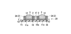
- FIG. 9B is a cross-sectional view of the solar cell in the manufacturing process shown in FIG. 9A, taken along line Y2-Y2.
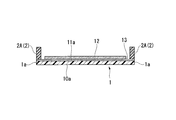
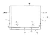
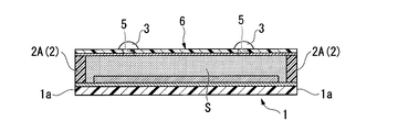
- the manufacturing method of the solar cell of this embodiment is as follows: (1) As shown in FIG. 1 and FIG. 2, a step of disposing an electrolyte on a plate-like first electrode 1, wherein the electrolyte is placed on a pair of opposing sides of the plate-like first electrode. Supplying a region sandwiched between a pair of first sealing portions 2A provided along the side 1a; (2) As shown in FIGS. 3 and 4, the second electrode in which holes 5 are formed in the plate surface of the flexible plate-like substrate 10 b so as to penetrate the thickness direction and discharge the electrolyte 3.
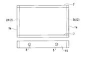
- a process of attaching (3) As shown in FIG. 5 to FIG. 7, it extends in the direction crossing the side 1a between the pair of first sealing portions 2 and 2, and is spaced in the direction along the side 1a.
- the holes 5 are arranged so as to be located outside the region sandwiched between the second sealing portions 7 and 7.
- Step of filling electrolyte 3 In the step of filling electrolyte 3, a pair of first seals provided along a pair of side edges 1a facing each other of plate-like first electrode 1 shown in FIG. As shown in FIG. 2, a liquid, semi-solid or solid electrolyte 3 is supplied to a region sandwiched between the stopping portions 2 and 2.
- the first electrode 1 is preferably formed by forming the conductive film 11a on the surface of the substrate 10a and further forming the semiconductor layer 12 on the surface of the conductive film 11a.
- the first electrode 1 is preferably formed in a substantially rectangular shape.
- a material of the substrate 10a used for the first electrode for example, a resin material or a glass substrate or the like mainly made of a transparent thermoplastic resin material such as polyethylene naphthalate (PEN) or polyethylene terephthalate (PET) is preferably used. Can be used.
- the substrate 10a is preferably formed in a flexible film shape.
- Examples of the material of the conductive film 11a include tin-doped indium oxide (ITO), zinc oxide, fluorine-doped tin oxide (FTO), aluminum-doped zinc oxide (AZO), tin oxide (SnO), antimony-doped tin oxide (ATO), Indium oxide / zinc oxide (IZO), gallium-doped zinc oxide (GZO), or the like can be used.
- ITO indium oxide
- FTO fluorine-doped tin oxide
- AZO aluminum-doped zinc oxide
- SnO tin oxide
- ATO antimony-doped tin oxide
- IZO Indium oxide / zinc oxide
- GZO gallium-doped zinc oxide
- the semiconductor layer 12 has a function of receiving and transporting electrons from a sensitizing dye described later, and a semiconductor made of a metal oxide, an organic metal, or the like is formed on the surface of the conductive film 11a.
- a metal oxide for example, titanium oxide (TiO 2 ), zinc oxide (ZnO), tin oxide (SnO 2 ), or the like can be used.
- an organic metal having a perovskite structure such as CH 3 NH 3 PbX 3 (X is a halogen atom) can be used.
- the semiconductor layer 12 can carry a sensitizing dye.
- the sensitizing dye supported on the semiconductor layer 12 is composed of an organic dye or a metal complex dye.
- the organic dye for example, various organic dyes such as coumarin, polyene, cyanine, hemicyanine, and thiophene can be used.
- the metal complex dye for example, a ruthenium complex is preferably used.
- a pair of sealing materials 2A are continuously arranged in the depth direction of the paper along the side edge 1a at both ends in the width direction of the substrate 10a (that is, the direction intersecting the side edge 1a extending in the depth direction of the paper surface).
- an adhesive for example, a hot melt resin
- a curable resin can be suitably used.
- the pair of sealing materials 2 ⁇ / b> A and 2 ⁇ / b> A that face each other serve as side walls that prevent the electrolyte 3 from flowing down on both sides in the width direction of the first electrode 1.
- the sealing material 2A disposed at both ends in the width direction of the first electrode 1 is a first sealing portion that seals the first electrode 1 and the second electrode 6 in the side 1a direction at both ends in the width direction. 2 is constituted.
- the electrolyte 3 is filled between the sealing materials 2 ⁇ / b> A of the first electrode 1, that is, a region sandwiched between the first sealing portions 2 and 2.
- the amount of the electrolyte 3 to be filled is more than the electrolyte 3 finally sealed between the first electrode 1 and the second electrode 6 so as not to overflow to the outside between the first sealing portions 2 and 2. Also make more. Therefore, as shown in FIG. 2, the electrolyte 3 is filled to such an extent that it protrudes slightly above the line connecting the upper ends of the sealing materials 2A and 2A.
- Examples of the electrolyte 3 include nonaqueous solvents such as acetonitrile and propionitrile; liquid components such as ionic liquids such as dimethylpropylimidazolium iodide or butylmethylimidazolium iodide; and a supporting electrolyte such as lithium iodide; A solution mixed with iodine can be used.
- the electrolyte 3 may be one containing t-butylpyridine in order to prevent reverse electron transfer reaction.
- Step of adhering the first electrode 1 and the second electrode 6 in the first sealing portion 2 As shown in FIGS. 3 and 4, the first electrode 1 in the first sealing portion 2 In the step of attaching the second electrode 6 to the first electrode 1, the second electrode 6 having a hole 5 that penetrates in the thickness direction and can discharge the electrolyte 3 is formed along the side 1 a with respect to the first electrode 1.
- the second electrode 6 and the first electrode 1 are adhered to each other in the first sealing portions 2 and 2 as viewed in the direction and gradually overlapped from the one end 6 m side toward the other end 6 n side.
- a conductive film 11b is formed on a substrate (also referred to as a base material) 10b.
- the material and shape of the substrate 10b can be formed in substantially the same manner as the substrate 10a of the first electrode 1 except that a hole 5 is formed in the thickness direction and a flexible material is used.
- the conductive film 11b of the second electrode 6 does not have a role of a catalyst layer (not shown) but has a role as the conductive film 11b, or a material that can function as both a catalyst layer (not shown) and the conductive film 11b. Either of these can be used.
- a catalyst layer (not shown) is further formed on the conductive film 11b.
- only the conductive film 11b is formed on another substrate 10b.
- a carbon paste, platinum, etc. can be employ
- a transparent substrate is used as at least one of the substrate 10a of the first electrode 1 and the substrate 10b of the second electrode 6. Moreover, at least one of the conductive films 11a and 11b of the first electrode 1 or the second electrode 6 is formed of a transparent conductive film.
- the bonding of the second electrode 6 to the first electrode 1 is performed as follows. That is, as shown in FIG. 3, the other end 6 n side of the second electrode 6 is lifted, and the one end 6 m side is bonded to the first electrode 1.
- the vicinity of the portion of the second electrode 6 bonded to the first electrode 1 is curved in a substantially arc shape. And the part where the 2nd electrode 6 became curved shape is bonded together to the 1st electrode 1 gradually toward the other end 6n side from the one end 6m side.
- heating and light irradiation are performed according to the material of the sealing material 2A while applying pressure on the first sealing portion 2, and the first electrode 1 and the second electrode 6 are pasted by the sealing material 2A.
- the first sealing portion 2 is slightly after the pressurization of the sealing materials 2 ⁇ / b> A and 2 ⁇ / b> A. , Level between the two parts with a roller.
- the electrolyte 3 disposed between the first sealing portions 2 and 2 is filled slightly larger than the final sealing amount, as shown in FIG.
- it is pressed from one end 6 m side to the other end 6 n side.
- the bubbles contained in the space S filled with the electrolyte 3 are pushed out from the bonding direction of the second electrode 6 to the first electrode 1, that is, from the one end 6m side to the other end 6n side.
- the surplus part of the electrolyte 3 is extruded toward the other end 6n side from the one end 6m side.
- the excess electrolyte 3 pushed out from the one end 6 m side toward the other end side 6 n gradually increases and overflows to the outside between the first sealing portions 2 in the second electrode 6. It is formed at a position (that is, closer to one end 6 m). Therefore, as shown in FIGS. 4 and 5, the holes 5 are formed by discharging the excess electrolyte 3 filled between the first sealing portions 2 and 2 of the first electrode 1. This prevents the electrolyte 3 from overflowing and adhering to the adhesive surface of the sealing material 2A forming the first sealing portion 2.
- Step of Sealing Space S Filled with Electrolyte 3 As shown in FIG. 5 to FIG. 7, in the step of sealing space S filled with electrolyte 3 (see FIG. 5), a pair of first seals The first electrode in the pair of second sealing portions 7, 7 extending between the stop portions 2 in the direction intersecting the side 1 a and spaced apart in the direction along the side 1 a. 1 and the 2nd electrode 6 are stuck. At this time, the second sealing portion 7 is set so that the hole 5 is located outside the region sandwiched between the second sealing portions 7 and 7.
- the second sealing portion 7 is provided across the width direction with an interval in the side 1a direction of the bonded first electrode 1 and second electrode 6.
- the first electrode 1 and the second electrode 6 are fused by using ultrasonic fusion or the like in the second sealing portion 7, and at least a part of the second sealing portion 7 is left. Preferably, it is completed by cutting outside the fused part of the second sealing part 7.
- the electrolyte 3 is pressed against the first electrode 1 in which the electrolyte 3 is filled in the region sandwiched between the first sealing portions 2 and 2.
- the second electrode 6 is bonded in one direction, the first electrode 1 and the second electrode 6 can be bonded together while removing bubbles present in the space filled with the electrolyte 3. Therefore, the method for manufacturing the solar cell according to the present embodiment has an effect that the deterioration of the quality of the solar cell due to the presence of bubbles in the solar cell filled with the electrolyte 3 can be prevented.
- the manufacturing method of the solar cell according to the present embodiment has an effect that it is possible to prevent the electrolyte 3 from adhering to the bonding surface of the sealing material 2A and thereby reducing the adhesive force of the sealing material 2A. can get.
- the constituent members of the solar cell can be arranged in the stacking order, so that an effect of facilitating manufacture and facilitating continuous production is obtained.
- the first electrode 1 and the second electrode 6 are ultrasonically positioned by positioning the hole 5 outside the region sandwiched between the second sealing portions 7 and 7. Therefore, the step of closing the hole 5 for discharging the electrolyte 3 and the step of removing the electrolyte 3 attached around the hole 5 can be omitted. Therefore, the solar cell manufacturing method of the present embodiment has an effect that the solar cell can be efficiently manufactured. Moreover, since the manufacturing method of the solar cell of this embodiment cut
- the method for manufacturing a solar cell according to the second embodiment is a method for continuously producing a plurality of power generation elements (solar cells) d, d... (That is, solar cell modules) connected in series.
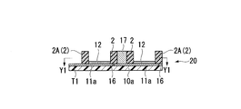
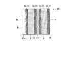
- Step of Filling Electrolyte 3 In the step of filling electrolyte 3 of the second embodiment, as shown in FIGS. 8A and 8B, a plurality of elongated strip-like conductive films 11a are formed on substrate 10a. The first electrode 20 in which the semiconductor layer 12 is formed on each conductive film 11a is used. Then, as shown in FIGS. 9A and 9B, a pair of first sealing portions 2, 2,... Along the side edge 1a is formed at both ends in the width direction (direction orthogonal to the longitudinal direction) of each conductive film 11a. Then, a liquid or semi-solid electrolyte 3 is filled between the first sealing portions 2 and 2.
- the substrate 10a is formed in a long strip shape.
- a plurality (two in this embodiment) of conductive films 11a and semiconductor layers 12 are formed adjacent to each other in the width direction of the substrate 10a.
- An insulating groove 16 extending in the side 1a direction is formed between the conductive films 11a.
- the sealing material 2A is formed at both ends in the width direction of one conductive film 11a so that one power generation element is formed on one conductive film 11a.
- a sealing material 2 ⁇ / b> A on one end side in the width direction (right side in the drawing in the present embodiment) is formed on the insulating groove 16.
- the electrolyte 3 is filled between the sealing materials 2A (that is, the first sealing portions 2) formed on the same conductive film 11a.
- a conductive material 17 for connecting adjacent power generating elements in series is disposed.
- the substrate 10a on which the conductive film 11a is formed is projected outside the region sandwiched between the first sealing portions 2, and the projected end portion
- the terminal can be taken out at T1.
- Step of sealing the space S filled with the electrolyte 3 As shown in FIGS. 10A, 10B, 11A, and 11B, the step of sealing the space S filled with the electrolyte 3 is the same as in the first embodiment.
- the second electrode 30 is bonded to the first electrode 20 in the same manner as shown.
- the pair of second sealing portions 7, 7 provided at intervals in the longitudinal direction is positioned so that the hole 5 is located outside the region sandwiched between the pair of second sealing portions 7, 7. Set to. Thereafter, the first electrode 20 and the second electrode 30 are fused and cut in the second sealing portion 7.
- the second electrode 30 is formed by forming a plurality of strip-like conductive films 11b and 11b on the substrate 10b.
- An insulating groove 18 is provided between the conductive films 11b and 11b to electrically insulate them.
- the insulating groove 18 of the second electrode 30 is disposed so as to be in contact with a sealing material 2A different from the sealing material 2A with which the insulating groove 16 of the first electrode 20 is in contact.
- one end side in the width direction of the substrate 10b is arranged so as to protrude outside the region sandwiched between the first sealing portions 2 and 2, and the terminal can be taken out at the protruding end T2.
- a solar cell module including a plurality of power generation elements d and d is provided in addition to the operations, functions, and effects shown in the first embodiment. , It can be efficiently manufactured in a continuous operation (so-called Roll to Roll), in which each process is processed while pulling out a roll-shaped substrate at one end, and the work is performed while winding in a roll at the other end. An effect is obtained.
- the present invention is not limited to the configurations shown in the first and second embodiments, and does not depart from the essence of the invention.
- Each configuration can be appropriately changed and applied in the range.
- the hole 5 may be provided in a region sandwiched between the second sealing portions 7 and 7. According to this structure, a solar cell can be easily manufactured by sticking in the second sealing portion 7 and sealing the hole 5.
- the shape and number of the holes 5 can be set as appropriate.
- the diameter of the hole 5 can be a dimension that satisfies the following relationship: 30 ⁇ m ⁇ hole diameter ⁇ the distance between the first sealing portions 2 and 2.
- the plurality of holes may be arranged at intervals in the width direction, or one hole 5 may be continuously opened in the width direction.
- the shape of the hole 5 may be a polygon such as a triangle other than a circle.
- the first sealing portion 2 is set only by disposing the sealing material 2A at both ends in the width direction of the first electrode 20, but the first sealing portion 12A and 12B, as shown in FIGS. 12A and 12B, both ends of the conductive film 3 in the width direction are raised to form the recessed portions 13 and sealed with the flange portions 40 and 40 to which the second electrode 30 can be bonded. It may be formed of the material 2A.
- the first electrodes 1 and 20 are photoelectrodes and the second electrodes 6 and 30 are counter electrodes.
- the second electrodes 6 and 30 are photoelectrodes
- the electrodes 1 and 20 may be used as counter electrodes.
- the manufacturing method of the solar cell of this invention can be applied suitably also to manufacture of the solar cell connected in parallel.
- the second sealing portions 7 and 7 in the first embodiment, the second embodiment, or the modifications thereof are preferably attached by ultrasonic fusion, but an adhesive or the like is used. It is also possible to do this.
- the 1st electrode part 50 is formed only by the flange 40 shown to FIG. 12A by taking out a terminal from the 2nd sealing part 7 suitably, and the 1st electrode 50 is shown. May be attached to the second electrode 6 by ultrasonic fusion.
Landscapes
- Engineering & Computer Science (AREA)
- Power Engineering (AREA)
- Chemical & Material Sciences (AREA)
- Chemical Kinetics & Catalysis (AREA)
- Electrochemistry (AREA)
- Microelectronics & Electronic Packaging (AREA)
- Manufacturing & Machinery (AREA)
- Materials Engineering (AREA)
- Photovoltaic Devices (AREA)
- Hybrid Cells (AREA)
- Life Sciences & Earth Sciences (AREA)
- Sustainable Development (AREA)
- Sustainable Energy (AREA)
Abstract
Description
本願は、2014年7月30日に、日本に出願された特願特願2014-155576号に基づき優先権を主張し、その内容をここに援用する。
そこで上記課題に鑑み、本発明は、液状等の電解質が充填される空間に気泡が残ることを防止して品質の高い太陽電池を製造する方法を提供する。
なお、本発明において、電解質とは液体又は半固体状の電解質をいう。
この構成によれば、電解質に混入した気泡を排出することができる。
この構成によれば、第1電極と第2電極との貼り合わせの後に必要となり得る孔から排出された電解質の後処理を省略して太陽電池を完成させることができる。
この構成によれば、電解質に混入した気泡の排出をすることができる。
この構成によれば、容易に第1の封止用部分を設定することができる。
本実施形態の太陽電池の製造方法は、
(1)図1,図2に示すように、板状の第1電極1上に電解質を配する工程であって、前記電解質を、前記板状の第1電極の互いに対向する一組の側辺1aに沿って設けられた一対の第1の封止用部分2Aに挟まれた領域に供給する工程と、
(2)図3,図4に示すように、可撓性を有する板状基材10bの板面に、厚さ方向に貫通して電解質3を排出可能な孔5が形成された第2電極6を、第1電極1に側辺1aに沿う方向の一端6m側から他端6n側に向かって漸次重ね合せ、第1の封止用部分2において第2電極6と第1電極1とを貼着する工程と、
(3)図5-図7に示すように、一対の第1の封止用部分2,2の間に亘って側辺1aに交叉する方向に延びるとともに、側辺1aに沿う方向に間隔を空けて設定される一対の第2の封止用部分7において第1電極1と第2電極6とを貼着して、電解質3が充填された空間Sを密封する工程とを有し、ここで、孔5は、第2の封止用部分7,7に挟まれた領域の外側に位置するように配置されている。
電解質3を充填する工程では、図1に示す板状の第1電極1の互いに対向する一組の側辺1aに沿って設けられた一対の第1の封止用部分2,2に挟まれた領域に、図2に示すように液体、半固体又は固体状の電解質3を供給する。
第1電極1は、略矩形に形成しておくことが好ましい。
第1電極1に用いられる基板10aの材料としては、例えば、ポリエチレンナフタレート(PEN)、ポリエチレンテレフタレート(PET)等の透明の熱可塑性樹脂材料を主原料とする樹脂材料又はガラス基板等を好適に用いることができる。この基板10aは、可撓性のあるフィルム状に形成されたものであることが好ましい。
金属酸化物としては、例えば、酸化チタン(TiO2)、酸化亜鉛(ZnO)、酸化スズ(SnO2)等を用いることができる。有機金属としては、CH3NH3PbX3(Xはハロゲン原子)などのペロブスカイト構造の有機金属等を用いることができる。
封止材2Aとしては、接着剤(例えばホットメルト樹脂)又は硬化性樹脂等を好適に用いることができる。
具体的には、第1電極1の導電膜11aの表面には、一定の厚さを有する封止材2Aを配しておくことによって、液状又は半固体状の電解質3を充填させる凹み部13を形成しておくことが好ましい。これによって、対向する一対の封止材2A,2Aは、電解質3が第1電極1の幅方向両側方に流れ落ちないようにする側壁となる。また、第1電極1の幅方向両端に配された封止材2Aは、第1電極1と第2電極6とを幅方向両端で側辺1a方向に封止する第1の封止用部分2を構成している。
電解質3としては、例えば、アセトニトリル、プロピオニトリル等の非水系溶剤;ヨウ化ジメチルプロピルイミダゾリウム又はヨウ化ブチルメチルイミダゾリウム等のイオン液体などの液体成分に、ヨウ化リチウム等の支持電解液とヨウ素とが混合された溶液等を用いることができる。また、電解質3は、逆電子移動反応を防止するため、t-ブチルピリジンを含むものを用いてもよい。
図3,図4に示すように、第1の封止用部分2において第1電極1と第2電極6とを貼着する工程では、厚さ方向に貫通して電解質3を排出可能な孔5が形成された第2電極6を、第1電極1に対して側辺1aに沿う方向に視て一端6m側から他端6n側に向かってに漸次重ね合せ、第1の封止用部分2,2において第2電極6と第1電極1とを貼着する。
基板10bの材質及び形状は、厚さ方向に孔5が形成されている点及び可撓性を有するものを用いる点を除いて第1電極1の基板10aと略同様に形成することができる。
第2電極6の導電膜11bには、不図示の触媒層の役割を有さず導電膜11bとしての役割を有する材料か、不図示の触媒層及び導電膜11bの双方の役割を果たし得る材料のいずれかを用いることができる。前者の場合は、導電膜11b上に更に不図示の触媒層が成膜されており、後者の場合には導電膜11bのみが他の基板10bに成膜されている構成とすることができる。
また、導電膜11bの表面に成膜される触媒層としては、カーボンペースト,プラチナ等を採用することができる。
また、第1電極1又は第2電極6の少なくともいずれか一方の導電膜11a,11bは、透明導電膜により形成しておく。
すなわち、図3に示すように、第2電極6の他端6n側を持ち上げ、一端6m側を第1電極1に貼り合わせる。第1電極1と貼り合わされた第2電極6の部分の近傍を略円弧状に湾曲させておく。そして、第2電極6が湾曲形状になった部分を一端6m側から他端6n側に向かって漸次第1電極1に貼り合わせる。
したがって、孔5は、図4,図5に示すように、第1電極1の第1の封止用部分2,2間に多めに充填された余剰分の電解質3を排出することにより、余剰の電解質3が溢流して第1の封止用部分2を形成している封止材2Aの接着面に付着することを防止する。
図5-図7に示すように、電解質3が充填された空間S(図5参照)を密封する工程では、一対の第1の封止用部分2の間に亘って側辺1aに交叉する方向に延びるとともに、側辺1aに沿う方向に間隔を空けて設定される一対の第2の封止用部分7,7において第1電極1と第2電極6とを貼着する。この際、第2の封止用部分7は、孔5が第2の封止用部分7,7に挟まれた領域の外側に位置するように設定する。
また、本実施形態の太陽電池の製造方法によれば、太陽電池の構成部材をその積層順に配することができるため、製造が容易となり連続生産を行いやすくなるという効果が得られる。
第2の実施形態の太陽電池の製造方法は、直列接続させた複数の発電素子(太陽電池)d,d・・(すなわち太陽電池モジュール)を連続生産する方法である。
第2の実施形態の電解質3を充填する工程では、図8A及び図8Bに示すように、基板10aに複数の長尺な帯状の導電膜11aを形成するとともに、各導電膜11aに半導体層12を形成した第1電極20を用いている。そして、図9A及び図9Bに示すように各導電膜11aの幅方向(長手方向に直交する方向)の両端に側辺1aに沿う一対の第1の封止用部分2,2・・を形成し、第1の封止用部分2,2同士の間に液体又は半固体状の電解質3を充填する。
導電膜11a同士の間には、側辺1a方向に延びる絶縁溝16が形成されている。
同じ導電膜11a上に形成された封止材2A(すなわち第1の封止用部分2同士)の間に電解質3を充填する。
封止材2A,2A同士の間には、隣り合う発電素子を直列接続させる導電材17が配されている。また、基板10aの幅方向の他端側には、第1の封止用部分2に挟まれた領域の外に導電膜11aを成膜させた基板10aを突出させ、この突出させた端部T1において端子の取出しができるようにする。
図10A、図10B、図11A、図11Bに示すように、電解質3が充填された空間Sを密封する工程では、第1実施形態で示した手法と同様にして第2電極30を第1電極20に貼り合わせる。そして、長手方向に間隔を空けて設ける一対の第2の封止用部分7,7を、一対の第2の封止用部分7,7に挟まれた領域の外に孔5を位置させるように設定する。その後、第2の封止用部分7において第1電極20及び第2電極30を融着し、切断する。
第2電極30の絶縁溝18は、図10Aに示すように、第1電極20の絶縁溝16が接している封止材2Aと異なる封止材2Aに接するように配する。また、基板10bの幅方向の一端側が、第1の封止用部分2,2に挟まれた領域の外に突出するように配し、この突出させた端部T2において端子の取出しができるようにする。
具体的には、第1の実施形態及び第2の実施形態において、孔5は第2の封止用部分7,7に挟まれた領域内に設けてもよい。
この構成によれば、第2の封止用部分7における貼着及び孔5の封止により簡便に太陽電池を製造することができる。
なお、本発明の太陽電池の製造方法は、並列接続の太陽電池の製造にも適宜応用することができる。
また、第1の実施形態については、第2の封止用部分7から端子を適宜取出すことにより、第1の封止用部分2を図12Aに示すフランジ40のみにより形成し、第1電極50を用いて超音波融着により第2電極6と貼着させてもよい。
1a 側辺
2A 第1の封止用部分
5 孔
6 第2電極
7 第2の封止用部分
10a,10b 基板(基材)
Claims (4)
- 板状の第1電極上に電解質を配する工程であって、前記電解質を、前記板状の第1電極の互いに対向する一組の側辺に沿って設けられた一対の第1の封止用部分に挟まれた領域に供給する工程と、
可撓性を有する板状基材の板面に、厚さ方向に貫通して前記電解質を排出可能な孔が形成された第2電極を、前記第1電極に前記側辺に沿う方向の一端側から他端側に向けて漸次重ね合せ、前記第1の封止用部分において前記第2電極と前記第1電極とを貼着する工程と、
前記一対の第1の封止用部分の間に亘って前記側辺に交叉する方向に延びるとともに、前記側辺に沿う方向に間隔を空けて設定される一対の第2の封止用部分において前記第1電極と前記第2電極とを貼着し、前記電解質が充填された空間を密封する工程とを有し、
前記孔は、前記一対の第2の封止用部分に挟まれた領域の外側に位置するように配置されている
ことを特徴とする太陽電池の製造方法。 - 前記密封する工程では、前記第2の封止用部分で前記第2電極と前記第1電極とを貼着し、前記第2の封止用部分の少なくとも一部を残して切断することを特徴とする請求項1に記載の太陽電池の製造方法。
- 板状の第1電極上に電解質を配する工程であって、前記電解質を、前記板状の第1電極の互いに対向する一組の側辺に沿って設けられた一対の第1の封止用部分に挟まれた領域に供給する工程と、
可撓性を有する板状基材の板面に、厚さ方向に貫通して前記電解質を排出可能な孔が形成された第2電極を、前記第1電極に前記側辺に沿う方向の一端側から他端側に向けて漸次重ね合せ、前記第1の封止用部分において前記第2電極と前記第1電極とを貼着する工程と、
前記一対の第1の封止用部分の間に亘って前記側辺に交叉する方向に延びるとともに、前記側辺に沿う方向に間隔を空けて設定される一対の第2の封止用部分において前記第1電極と前記第2電極とを貼着し、前記電解質が充填された空間を密封する工程とを有し、
前記孔は、前記一対の第2の封止用部分に挟まれた領域内に位置するように配置されており、前記第2電極を前記第1電極に重ね合せた後に封止される
ことを特徴とする太陽電池の製造方法。 - 前記第1の封止用部分は、前記一組の側辺に沿って設置された封止材であることを特徴とする請求項1から3のいずれか一項に記載の太陽電池の製造方法。
Priority Applications (4)
| Application Number | Priority Date | Filing Date | Title |
|---|---|---|---|
| CN201580041719.2A CN106575581B (zh) | 2014-07-30 | 2015-07-30 | 太阳能电池的制造方法 |
| KR1020177002667A KR20170033325A (ko) | 2014-07-30 | 2015-07-30 | 태양 전지의 제조 방법 |
| JP2016538448A JPWO2016017776A1 (ja) | 2014-07-30 | 2015-07-30 | 太陽電池の製造方法 |
| US15/326,815 US9991058B2 (en) | 2014-07-30 | 2015-07-30 | Method for manufacturing solar cell |
Applications Claiming Priority (2)
| Application Number | Priority Date | Filing Date | Title |
|---|---|---|---|
| JP2014155576 | 2014-07-30 | ||
| JP2014-155576 | 2014-07-30 |
Publications (1)
| Publication Number | Publication Date |
|---|---|
| WO2016017776A1 true WO2016017776A1 (ja) | 2016-02-04 |
Family
ID=55217672
Family Applications (1)
| Application Number | Title | Priority Date | Filing Date |
|---|---|---|---|
| PCT/JP2015/071706 Ceased WO2016017776A1 (ja) | 2014-07-30 | 2015-07-30 | 太陽電池の製造方法 |
Country Status (6)
| Country | Link |
|---|---|
| US (1) | US9991058B2 (ja) |
| JP (1) | JPWO2016017776A1 (ja) |
| KR (1) | KR20170033325A (ja) |
| CN (1) | CN106575581B (ja) |
| TW (1) | TWI665694B (ja) |
| WO (1) | WO2016017776A1 (ja) |
Cited By (4)
| Publication number | Priority date | Publication date | Assignee | Title |
|---|---|---|---|---|
| JP2017163024A (ja) * | 2016-03-10 | 2017-09-14 | 日本ゼオン株式会社 | 色素増感型太陽電池モジュールの製造方法 |
| JP2020038877A (ja) * | 2018-09-03 | 2020-03-12 | 積水化学工業株式会社 | 電気モジュールおよび電気モジュールの製造方法 |
| JP2020038876A (ja) * | 2018-09-03 | 2020-03-12 | 積水化学工業株式会社 | 電気モジュール |
| US10618873B2 (en) | 2016-02-01 | 2020-04-14 | Basf Se | Method for producing C4-C15 lactams |
Families Citing this family (1)
| Publication number | Priority date | Publication date | Assignee | Title |
|---|---|---|---|---|
| CN113921622B (zh) * | 2021-09-30 | 2024-04-05 | 中国科学院苏州纳米技术与纳米仿生研究所 | 电池片基板、光伏电池、光伏电池组件及其组装方法 |
Citations (5)
| Publication number | Priority date | Publication date | Assignee | Title |
|---|---|---|---|---|
| JP2007220608A (ja) * | 2006-02-20 | 2007-08-30 | Dainippon Printing Co Ltd | 色素増感型太陽電池の製造方法および色素増感型太陽電池 |
| JP2007287483A (ja) * | 2006-04-17 | 2007-11-01 | Fujikura Ltd | 色素増感太陽電池 |
| JP2008130537A (ja) * | 2006-11-17 | 2008-06-05 | Samsung Sdi Co Ltd | 染料感応太陽電池用高分子ゲル電解質組成物、染料感応太陽電池及び染料感応太陽電池の製造方法 |
| JP2012209139A (ja) * | 2011-03-30 | 2012-10-25 | Toyo Seikan Kaisha Ltd | 液状物の充填封止方法 |
| JP2014063565A (ja) * | 2009-07-28 | 2014-04-10 | Fujikura Ltd | 色素増感型太陽電池の製造方法 |
Family Cites Families (16)
| Publication number | Priority date | Publication date | Assignee | Title |
|---|---|---|---|---|
| KR100567331B1 (ko) * | 2004-08-04 | 2006-04-04 | 한국전자통신연구원 | 레고형 염료감응 태양전지 모듈 |
| CN101604708A (zh) * | 2008-06-14 | 2009-12-16 | 大连七色光太阳能科技开发有限公司 | 复合透明导电基板 |
| CN201302932Y (zh) * | 2008-12-10 | 2009-09-02 | 大连七色光太阳能科技开发有限公司 | 一种染料敏化太阳能电池的电极结构 |
| KR101386578B1 (ko) * | 2009-12-24 | 2014-04-21 | 엘지디스플레이 주식회사 | 염료감응 태양전지 |
| CN102194577B (zh) * | 2010-03-10 | 2013-02-06 | 北京大学 | 太阳能电池及其制造方法 |
| JP2011204522A (ja) | 2010-03-26 | 2011-10-13 | Spd Laboratory Inc | 色素増感太陽電池モジュールおよびその製造方法 |
| KR101050470B1 (ko) * | 2010-04-05 | 2011-07-20 | 삼성에스디아이 주식회사 | 루테늄 착체 및 이를 이용한 염료감응 태양전지 |
| KR101146673B1 (ko) * | 2010-05-06 | 2012-05-22 | 삼성에스디아이 주식회사 | 염료감응 태양전지용 전극, 그 제조방법 및 이를 이용한 염료감응 태양전지 |
| KR101137379B1 (ko) * | 2010-11-23 | 2012-04-20 | 삼성에스디아이 주식회사 | 염료감응 태양전지용 겔형 전해질 및 이를 포함하는 염료감응 태양전지 |
| KR101234239B1 (ko) * | 2011-01-21 | 2013-02-18 | 삼성에스디아이 주식회사 | 염료감응 태양전지 및 그 제조방법 |
| WO2013110948A1 (en) * | 2012-01-26 | 2013-08-01 | Bangor University | Method for re-dyeing dye sensitised solar cells |
| KR101192981B1 (ko) * | 2012-05-15 | 2012-10-19 | 주식회사 상보 | 금속 플렉시블 염료감응 태양전지 및 그 제조방법 |
| KR101689982B1 (ko) * | 2012-09-18 | 2016-12-26 | 도쿄 유니버시티 오브 사이언스 에듀케이셔널 파운데이션 애드미니스트레이티브 오거니제이션 | 색소 증감 태양 전지용 대향 전극 및 색소 증감 태양 전지 |
| JP2014082187A (ja) * | 2012-09-28 | 2014-05-08 | Fujifilm Corp | 光電変換素子および色素増感太陽電池 |
| JP6224003B2 (ja) * | 2012-12-14 | 2017-11-01 | シャープ株式会社 | 光電変換素子 |
| KR20140112141A (ko) * | 2013-03-11 | 2014-09-23 | 삼성에스디아이 주식회사 | 염료감응 태양전지용 전해질 및 이를 이용한 염료감응 태양전지 |
-
2015
- 2015-07-30 TW TW104124845A patent/TWI665694B/zh not_active IP Right Cessation
- 2015-07-30 KR KR1020177002667A patent/KR20170033325A/ko not_active Withdrawn
- 2015-07-30 JP JP2016538448A patent/JPWO2016017776A1/ja not_active Withdrawn
- 2015-07-30 US US15/326,815 patent/US9991058B2/en active Active
- 2015-07-30 CN CN201580041719.2A patent/CN106575581B/zh not_active Expired - Fee Related
- 2015-07-30 WO PCT/JP2015/071706 patent/WO2016017776A1/ja not_active Ceased
Patent Citations (5)
| Publication number | Priority date | Publication date | Assignee | Title |
|---|---|---|---|---|
| JP2007220608A (ja) * | 2006-02-20 | 2007-08-30 | Dainippon Printing Co Ltd | 色素増感型太陽電池の製造方法および色素増感型太陽電池 |
| JP2007287483A (ja) * | 2006-04-17 | 2007-11-01 | Fujikura Ltd | 色素増感太陽電池 |
| JP2008130537A (ja) * | 2006-11-17 | 2008-06-05 | Samsung Sdi Co Ltd | 染料感応太陽電池用高分子ゲル電解質組成物、染料感応太陽電池及び染料感応太陽電池の製造方法 |
| JP2014063565A (ja) * | 2009-07-28 | 2014-04-10 | Fujikura Ltd | 色素増感型太陽電池の製造方法 |
| JP2012209139A (ja) * | 2011-03-30 | 2012-10-25 | Toyo Seikan Kaisha Ltd | 液状物の充填封止方法 |
Cited By (6)
| Publication number | Priority date | Publication date | Assignee | Title |
|---|---|---|---|---|
| US10618873B2 (en) | 2016-02-01 | 2020-04-14 | Basf Se | Method for producing C4-C15 lactams |
| JP2017163024A (ja) * | 2016-03-10 | 2017-09-14 | 日本ゼオン株式会社 | 色素増感型太陽電池モジュールの製造方法 |
| JP2020038877A (ja) * | 2018-09-03 | 2020-03-12 | 積水化学工業株式会社 | 電気モジュールおよび電気モジュールの製造方法 |
| JP2020038876A (ja) * | 2018-09-03 | 2020-03-12 | 積水化学工業株式会社 | 電気モジュール |
| JP7107788B2 (ja) | 2018-09-03 | 2022-07-27 | 積水化学工業株式会社 | 電気モジュールおよび電気モジュールの製造方法 |
| JP7164362B2 (ja) | 2018-09-03 | 2022-11-01 | 積水化学工業株式会社 | 電気モジュール |
Also Published As
| Publication number | Publication date |
|---|---|
| TW201618141A (zh) | 2016-05-16 |
| US20170213654A1 (en) | 2017-07-27 |
| US9991058B2 (en) | 2018-06-05 |
| CN106575581B (zh) | 2018-11-27 |
| KR20170033325A (ko) | 2017-03-24 |
| TWI665694B (zh) | 2019-07-11 |
| CN106575581A (zh) | 2017-04-19 |
| JPWO2016017776A1 (ja) | 2017-06-01 |
Similar Documents
| Publication | Publication Date | Title |
|---|---|---|
| JPWO2016017776A1 (ja) | 太陽電池の製造方法 | |
| JP6286110B2 (ja) | 電気モジュールの製造方法および電気モジュールの製造装置 | |
| TWI640102B (zh) | 光電轉換元件及光電轉換元件之製造方法 | |
| JP6918521B2 (ja) | 電気モジュールおよび電気モジュールの製造方法 | |
| TW201444106A (zh) | 電氣裝置及電氣裝置之製造方法 | |
| JP2018037606A (ja) | 電気モジュールおよびその製造方法 | |
| JP5778601B2 (ja) | 電気モジュールの製造方法 | |
| JP6374774B2 (ja) | 太陽電池の製造方法 | |
| JP6166752B2 (ja) | 電気モジュール製造用部材 | |
| WO2017099217A1 (ja) | 電気モジュールおよびその製造方法 | |
| WO2019146684A1 (ja) | 電気モジュール及び電気モジュールの製造方法 | |
| JP5688344B2 (ja) | 電気モジュール及び電気モジュールの製造方法 | |
| JP6760885B2 (ja) | 電気モジュール及び電気モジュールの製造方法 | |
| JP7107788B2 (ja) | 電気モジュールおよび電気モジュールの製造方法 | |
| JP6703574B2 (ja) | 電気モジュールおよびその製造方法 | |
| JP6595894B2 (ja) | 粘性体供給装置、及び色素増感太陽電池の製造方法 | |
| JP2015099741A (ja) | フィルムデバイス | |
| WO2015083738A1 (ja) | 封止機能付導通材、電気モジュール、電気モジュールの製造方法 | |
| JP2020038876A (ja) | 電気モジュール | |
| TW201742287A (zh) | 太陽電池 | |
| TW202021145A (zh) | 太陽電池模組及附保護層之太陽電池模組 | |
| JP2019113627A (ja) | 調光シートの製造方法、及び調光シート製造用ロール体 |
Legal Events
| Date | Code | Title | Description |
|---|---|---|---|
| 121 | Ep: the epo has been informed by wipo that ep was designated in this application |
Ref document number: 15827267 Country of ref document: EP Kind code of ref document: A1 |
|
| WWE | Wipo information: entry into national phase |
Ref document number: 15326815 Country of ref document: US |
|
| ENP | Entry into the national phase |
Ref document number: 2016538448 Country of ref document: JP Kind code of ref document: A |
|
| NENP | Non-entry into the national phase |
Ref country code: DE |
|
| ENP | Entry into the national phase |
Ref document number: 20177002667 Country of ref document: KR Kind code of ref document: A |
|
| 122 | Ep: pct application non-entry in european phase |
Ref document number: 15827267 Country of ref document: EP Kind code of ref document: A1 |