WO2016017546A1 - 酸化インジウム系酸化物焼結体とその製造方法 - Google Patents
酸化インジウム系酸化物焼結体とその製造方法 Download PDFInfo
- Publication number
- WO2016017546A1 WO2016017546A1 PCT/JP2015/071125 JP2015071125W WO2016017546A1 WO 2016017546 A1 WO2016017546 A1 WO 2016017546A1 JP 2015071125 W JP2015071125 W JP 2015071125W WO 2016017546 A1 WO2016017546 A1 WO 2016017546A1
- Authority
- WO
- WIPO (PCT)
- Prior art keywords
- oxide
- sintered body
- oxide sintered
- less
- powder
- Prior art date
- Legal status (The legal status is an assumption and is not a legal conclusion. Google has not performed a legal analysis and makes no representation as to the accuracy of the status listed.)
- Ceased
Links
Classifications
-
- C—CHEMISTRY; METALLURGY
- C04—CEMENTS; CONCRETE; ARTIFICIAL STONE; CERAMICS; REFRACTORIES
- C04B—LIME, MAGNESIA; SLAG; CEMENTS; COMPOSITIONS THEREOF, e.g. MORTARS, CONCRETE OR LIKE BUILDING MATERIALS; ARTIFICIAL STONE; CERAMICS; REFRACTORIES; TREATMENT OF NATURAL STONE
- C04B35/00—Shaped ceramic products characterised by their composition; Ceramics compositions; Processing powders of inorganic compounds preparatory to the manufacturing of ceramic products
-
- C—CHEMISTRY; METALLURGY
- C23—COATING METALLIC MATERIAL; COATING MATERIAL WITH METALLIC MATERIAL; CHEMICAL SURFACE TREATMENT; DIFFUSION TREATMENT OF METALLIC MATERIAL; COATING BY VACUUM EVAPORATION, BY SPUTTERING, BY ION IMPLANTATION OR BY CHEMICAL VAPOUR DEPOSITION, IN GENERAL; INHIBITING CORROSION OF METALLIC MATERIAL OR INCRUSTATION IN GENERAL
- C23C—COATING METALLIC MATERIAL; COATING MATERIAL WITH METALLIC MATERIAL; SURFACE TREATMENT OF METALLIC MATERIAL BY DIFFUSION INTO THE SURFACE, BY CHEMICAL CONVERSION OR SUBSTITUTION; COATING BY VACUUM EVAPORATION, BY SPUTTERING, BY ION IMPLANTATION OR BY CHEMICAL VAPOUR DEPOSITION, IN GENERAL
- C23C14/00—Coating by vacuum evaporation, by sputtering or by ion implantation of the coating forming material
- C23C14/22—Coating by vacuum evaporation, by sputtering or by ion implantation of the coating forming material characterised by the process of coating
- C23C14/34—Sputtering
Definitions
- the present invention relates to an indium oxide-based oxide sintered body and a method for producing the same.
- the present invention also relates to a sputtering target using the indium oxide-based oxide sintered body as a target material.
- the transparent conductive oxide film Since the transparent conductive oxide film has high conductivity and high transmittance in the visible light region, it is used for transparent electrodes of solar cells, liquid crystal display elements, and other various light receiving elements. Further, it is also widely used as a transparent heating element for anti-fogging, such as a heat ray reflective film such as a window glass of an automobile or a building, various antistatic films, and a refrigeration showcase.
- a transparent heating element for anti-fogging such as a heat ray reflective film such as a window glass of an automobile or a building, various antistatic films, and a refrigeration showcase.
- an indium oxide (In 2 O 3 + ⁇ ) oxide film, a zinc oxide (ZnO + ⁇ ) oxide film, and a tin oxide (SnO 2 + ⁇ ) oxide film are widely used.
- indium oxide-based oxide films are most often used.
- indium oxide films containing tin oxide as a dopant are ITO (Indium Tin Oxide) films.
- the transparent conductive oxide film having a low resistance is easily obtained, and is widely used.
- optically effective oxide films are also known, and are applied as laminates in which the characteristics of each oxide film are precisely combined.
- a typical example is an antireflection film having a multilayer structure designed to selectively reflect or transmit light of a specific wavelength.
- functional multilayer films optical films with added values such as antistatic and electromagnetic wave shielding have been proposed.
- the spectral characteristics of the antireflection film having a multilayer structure are determined by the refractive index (n), extinction coefficient (k), and film thickness (d) of each layer. That is, the configuration of the laminate is determined by calculation based on the refractive index, extinction coefficient, and film thickness data of each layer constituting the multilayer film.
- a multilayer film (optical film) having more excellent optical characteristics is realized by combining a high refractive index film and a low refractive index film and incorporating an intermediate refractive index film as necessary. .
- n> 1.9 oxides such as titanium (Ti), cerium (Ce), zirconium (Zr), niobium (Nb), tantalum (Ta), and hafnium (Hf) are used.
- oxides such as titanium (Ti), cerium (Ce), zirconium (Zr), niobium (Nb), tantalum (Ta), and hafnium (Hf) are used.
- oxides such as titanium (Ti), cerium (Ce), zirconium (Zr), niobium (Nb), tantalum (Ta), and hafnium (Hf) are used.
- the low refractive index material an oxide of silicon (Si) is used.
- Examples of methods for forming these oxide films include sputtering, vapor deposition, and ion plating.
- the sputtering method is known as an effective means when a material having a low vapor pressure is formed or when precise film thickness control is required.
- Sputtering methods are classified according to the generation method of plasma into a high frequency sputtering method using high frequency plasma, a direct current sputtering method using direct current plasma, and the like.
- the direct current sputtering method is widely used industrially because the film forming speed is relatively fast, the power supply equipment is inexpensive, and the film forming operation is simple.
- the oxides that are the materials of the oxide film having a high refractive index are all poor in conductivity, and when these oxide sputtering targets are used, stable film formation by the DC sputtering method is not possible. Can not. Therefore, when an oxide film having a high refractive index is formed by direct current sputtering, sputtering is performed while reacting metal particles and oxygen in an oxygen-rich atmosphere using a conductive metal target. A so-called reactive sputtering method is used. However, the reactive sputtering method has the disadvantages that the deposition rate is extremely slow and the productivity is low. For this reason, it is difficult to reduce the manufacturing cost, and the film forming process using the reactive sputtering method is a serious problem in manufacturing an oxide film having a high refractive index.
- JP-A-9-176841 discloses indium oxide (In 2 O 3 ) and cerium oxide (Ce 2 O 3 ) as main components, and a small amount of tin oxide (SnO) and / or titanium oxide (A sputtering target made of an oxide sintered body to which TiO 2 ) is added is disclosed.
- This sputtering target is excellent in conductivity, can be subjected to direct current sputtering, and a transparent conductive oxide film obtained from this target has a high refractive index (about 2.3).
- this transparent conductive oxide film has an extinction coefficient of 5.0 ⁇ 10 ⁇ 2 or more on the short wavelength side in the visible region, and has sufficient transparency as a constituent material of an antireflection film having a multilayer structure. I can't say that.
- Japanese Patent Application Laid-Open Nos. 9-259640 and 2010-10347 include indium oxide (In 2 O 3 ) as a main component and a predetermined amount of gallium (Ga) added thereto, or in addition to these.
- An oxide sintered body to which tin (Sn), titanium (Ti), zirconium (Zr) and the like are added is disclosed.
- this oxide sintered body as a film forming material, the light transmittance (extinction coefficient) of the obtained transparent conductive oxide thin film is improved.
- these technologies are intended for touch panels and thin film solar cells, and are not intended for optical films such as antireflection films.
- Japanese Patent Application Laid-Open No. 9-111444 discloses that a zinc oxide powder as a raw material for producing an indium oxide-zinc oxide based sintered body target is 400 ° C. to A method of calcining at 800 ° C., mixing the calcined zinc oxide powder and indium oxide powder, press-molding the mixed powder, and then sintering at 1200 ° C. to 1400 ° C. is disclosed.
- the color unevenness of the oxide sintered body is considered to be due to the oxygen non-stoichiometry of zinc oxide, and by pre-calcining zinc oxide, the activity as zinc oxide powder is reduced, This suppresses the occurrence of color unevenness.
- white spots having a lighter color than the peripheral portion and a diameter of about 0.5 mm to 5 mm may be generated on the surface of the oxide sintered body.
- the resistance value of the white spot is larger than that of the peripheral portion, and when this oxide sintered body is formed as a sputtering target, the white spot becomes the starting point of arcing (abnormal discharge) and nodules.
- Japanese Patent Application Laid-Open No. 2011-11613 discloses a method of adding a color unevenness inhibitor made of a rare earth oxide such as cerium oxide or praseodymium oxide to a raw material powder when manufacturing an indium oxide-zinc oxide target. Has been. According to this method, white spots are not generated, but the properties of the oxide sintered body and the transparent conductive film formed using this as a target may be changed by the addition of the color unevenness preventing agent.
- a color unevenness inhibitor made of a rare earth oxide such as cerium oxide or praseodymium oxide
- JP 2010-150107 A discloses a mixed powder of a zinc compound powder and a powder containing at least one compound of an element selected from Al, Ga, B, Nb, In, Y, and Sc. Is disclosed in which a powder contact portion is filled in a mold other than a graphite-based material and hot-pressed at a temperature of 1000 ° C. to 1400 ° C. in a rare gas atmosphere. Yes. According to this method, since L * a * b * color difference: ⁇ E * measured in the CIE 1976 space between the surface from which the baked surface is removed and the center portion can be 3.0 or less, there is little color unevenness, It is possible to obtain an oxide sintered body having excellent discharge characteristic stability.
- the present invention provides a sputtering target capable of stably forming an optical film having a high refractive index and a low extinction coefficient on the short wavelength side of the visible region while suppressing the occurrence of arcing.
- an object of the present invention is to provide an oxide sintered body with less color unevenness and excellent uniformity of specific resistance, which makes it possible to provide such a sputtering target.
- the present invention relates to an indium oxide-based oxide sintered body containing indium oxide, gallium oxide, cerium oxide, and tin oxide and / or titanium oxide.
- the total content of indium oxide, gallium oxide, cerium oxide, tin oxide, and titanium oxide is 98.5 mol% or more, preferably 99.0 mol% or more, more preferably Is 99.5 mol% or more.
- (A) In atomic ratio: In / (In + Ga + Ce) is 0.30 to 0.54, preferably 0.36 to 0.50, more preferably 0.38 to 0.43
- (B) Ga atom ratio: Ga / (In + Ga + Ce) is 0.30 to 0.52, preferably 0.32 to 0.50, more preferably 0.35 to 0.48
- (C) Ce atom number ratio: Ce / (In + Ga + Ce) is 0.16-0.32, preferably 0.16-0.30, more preferably 0.17-0.28,
- D) Sn atom number ratio: Sn / (In + Ga + Ce + Sn + Ti) is 0.04 or less, preferably 0.020 to 0.035, more preferably 0.025 to 0.032.
- L * a * b * color difference: ⁇ E * measured in the CIE1976 space between the surface of the oxide sintered body and the thickness direction center position is 5.0 or less, preferably 4.0 or less. More preferably, it is 3.0 or less.
- L * a * b * color difference: ⁇ E ′ * measured in the CIE 1976 space between the radial central portion and the peripheral portion of the surface is 5.0 or less, preferably 4.0 or less, more preferably It is preferable that it is 3.0 or less.
- the specific resistance between the surface of the oxide sintered body and the central position in the thickness direction is preferably 1 ⁇ 10 5 ⁇ ⁇ cm or less, and preferably 0.5 ⁇ 10 5 ⁇ ⁇ cm or less. Further preferred.
- the relative density of the oxide sintered body is preferably 95.0% or more, more preferably 95.5% or more, and further preferably 96.0% or more.
- the production method for obtaining the indium oxide-based oxide sintered body according to the present invention is such that indium oxide powder, gallium oxide powder, cerium oxide powder, tin oxide powder and / or titanium oxide powder have the above composition ratio.
- the body is fired in an inert gas atmosphere to obtain an oxide sintered body.
- the sputtering target of the present invention is characterized by using the oxide sintered body as a target material.
- an oxide sintered body with little color unevenness and excellent uniformity of specific resistance can be obtained.
- an optical film having a high refractive index and a low extinction coefficient on the visible short wavelength side can be stably formed while suppressing the occurrence of arcing.
- a sputtering target that can be filmed can be provided. For this reason, the industrial significance of the present invention is extremely large.
- the inventors of the present invention added a predetermined amount of gallium (indium oxide-based oxide sintered body) as a sputtering target material for forming an optical film. It was found that by adding Ga) and cerium (Ce), an optical film having a low extinction coefficient on the short wavelength side in the visible region can be formed while having a high refractive index.
- Oxide sintered body “2. Manufacturing method of oxide sintered body”, and “3. Optical film”.
- the size of the oxide sintered body of the present invention is not limited, the short side is 5 inches (12.7 cm) ⁇ the long side is 15 inches (mainly the occurrence of color unevenness). 38.1 cm) ⁇ 0.7 inch (1.8 cm) or more of a large flat plate oxide sintered body will be described as an example.
- the present invention is not limited to application to such a large flat plate-shaped oxide sintered body, and various sizes of flat plate-shaped, disc-shaped, and cylindrical oxide sintered bodies and the use thereof are used. It can be applied to the sputtering target.
- large cylindrical oxide ceramics having an outer diameter of 4 inches (10.2 cm) or more, a thickness of 0.7 inches (1.8 cm) or more, and a total length of 2 inches (5.0 cm) or more.
- the present invention is suitably applied to a ligation and the like.
- the present invention relates to indium oxide, gallium oxide, cerium oxide, and indium oxide-based oxide sintered body containing tin oxide and / or titanium oxide (hereinafter referred to as “oxide sintered body”). About.
- This oxide sintered body is characterized in that the total content of indium oxide, gallium oxide, cerium oxide, tin oxide, and titanium oxide is 98.5 mol% or more.
- Ce Ce atomic ratio: Ce / (In + Ga + Ce) is 0.16-0.32, And the total number of atoms of In, Ga, Ce, tin (Sn) and titanium (Ti) in this oxide sintered body,
- D Ratio of Sn atoms: Sn / (In + Ga + Ce + Sn + Ti) is 0.04 or less,
- E Ti atom number ratio: Ti / (In + Ga + Ce + Sn + Ti) is 0.01 or less, These constituent components are uniformly dispersed.
- the oxide sintered body of the present invention is characterized in that L * a * b * color difference: ⁇ E * measured in the CIE 1976 space is 5.0 or less at the surface and in the center.
- Such an oxide sintered body has very little variation in resistance between the surface and the center. Therefore, when this oxide sintered body is used as a target, it is possible to form a transparent conductive film by a direct current sputtering method.
- the oxide sintered body of the present invention is composed of indium oxide, gallium oxide, cerium oxide, and tin oxide and / or titanium oxide. Components other than these components (additional components and inevitable impurities) may be included, but in this case, indium oxide, gallium oxide, cerium oxide, tin oxide, and titanium oxide contained in the oxide sintered body
- the total content of is required to be 98.5 mol% or more, preferably 99.0 mol% or more, more preferably 99.5 mol% or more.
- the total content of indium oxide, gallium oxide, cerium oxide, tin oxide, and titanium oxide is less than 98.5 mol%, that is, when the content of the additive component exceeds 1.5 mol%, the desired effect You will not be able to get.
- the content of In in the oxide sintered body is the ratio of the number of In atoms to the total number of In, Ga, and Ce atoms constituting the oxide sintered body: In / (In + Ga + Ce) (hereinafter, , “In / (In + Ga + Ce) atomic ratio”), 0.30 to 0.54, preferably 0.36 to 0.50, more preferably 0.38 to 0.43. .
- In / (In + Ga + Ce) atomic ratio is less than 0.36, the conductivity of the oxide sintered body is remarkably lowered, and film formation by the direct current sputtering method becomes impossible.
- the In / (In + Ga + Ce) atomic ratio exceeds 0.54, the desired effect cannot be obtained in relation to the content of other components.
- Ga is an element added to reduce the extinction coefficient on the short wavelength side of the visible region of an optical film obtained by forming a film using an oxide sintered body as a sputtering target.
- the content of Ga is the ratio of the number of Ga atoms to the total number of In, Ga, and Ce atoms constituting the oxide sintered body: Ga / (In + Ga + Ce) (hereinafter referred to as “Ga / (In + Ga + Ce) atoms”. Number ratio)) is required to be 0.30 to 0.52, preferably 0.32 to 0.50, more preferably 0.35 to 0.48. If the Ga / (In + Ga + Ce) atomic ratio is less than 0.30, the effect of reducing the extinction coefficient cannot be sufficiently obtained. On the other hand, if the Ga / (In + Ga + Ce) atomic ratio exceeds 0.48, the extinction coefficient can be reduced, but the desired effect cannot be obtained in relation to the content of other components. .
- Ce is an element added to improve the refractive index of an optical film obtained by forming a film using an oxide sintered body as a sputtering target.
- the Ce content is the ratio of the number of Ce atoms to the total number of In, Ga, and Ce atoms constituting the oxide sintered body: Ce / (In + Ga + Ce) (hereinafter referred to as “Ce / (In + Ga + Ce) atoms”.
- the number ratio is 0.16 to 0.32, preferably 0.16 to 0.30, and more preferably 0.17 to 0.28. If the Ce / (In + Ga + Ce) atomic ratio is less than 0.16, the refractive index cannot be sufficiently improved. On the other hand, if the Ce / (In + Ga + Ce) atomic ratio exceeds 0.32, the refractive index can be improved, but the desired effect cannot be obtained due to the content of other components.
- Sn and Ti are elements added to improve the relative density of the oxide sintered body and lower its specific resistance. At least one of Sn and Ti may be added, and it is not always necessary to add both Sn and Ti.
- Sn is the ratio of the number of Sn atoms to the total number of atoms of In, Ga, Ce, Sn, and Ti constituting this oxide sintered body: Sn / (In + Ga + Ce + Sn + Ti) (hereinafter, “Sn / (Referred to as “In + Ga + Ce + Sn + Ti) atomic ratio”), which is 0.040 or less, preferably 0.035 or less, and more preferably 0.032 or less.
- the Ti content is the ratio of the number of Ti atoms to the total number of In, Ga, Ce, Sn, and Ti atoms constituting the oxide sintered body: Ti / (In + Ga + Ce + Sn + Ti) (hereinafter, “ Ti / (In + Ga + Ce + Sn + Ti) atomic ratio ”), which is 0.010 or less, preferably 0.008 or less, more preferably 0.005 or less.
- Ti / (In + Ga + Ce + Sn + Ti) atomic ratio exceeds 0.040, or the Ti / (In + Ga + Ce + Sn + Ti) atomic ratio exceeds 0.010, the contents of In, Ga, and Ce are within the above-described ranges. However, the desired effect cannot be obtained.
- the lower limit of the Sn and Ti contents is not particularly limited, but in order to stably obtain the effect of improving the relative density, the Sn / (In + Ga + Ce + Sn + Ti) atomic ratio is 0.020 or more.
- the Ti / (In + Ga + Ce + Sn + Ti) atomic ratio is preferably 0.001 or more, the Sn / (In + Ga + Ce + Sn + Ti) atomic ratio is 0.025 or more, and the Ti / (In + Ga + Ce + Sn + Ti) atomic ratio is 0.003 or more. Is more preferable.
- the oxide sintered body of the present invention has an L * value measured in the CIE 1976 space, a * between the surface after removing the baked surface and the center position in the thickness direction of the oxide sintered body.
- L * a * b * color difference calculated from the following formula (1) based on the value and b * value: ⁇ E * value is 5.0 or less, preferably 4.5 or less, more preferably 4.0 or less, More preferably, it is 3.0 or less.
- L * a * b * is a color space based on the xyz color system developed by the International Commission on Illumination (CIE), and the L * value represents brightness (brightness), and a * b * The value represents hue and saturation.
- the a * value represents the position of red / magenta and green (a * ⁇ 0: position closer to green, a *> 0: position closer to positive magenta).
- the b * value represents a yellow and blue position (b * ⁇ 0: a position closer to blue, b *> 0: a position closer to yellow).
- the L * value, a * value, and b * value can be measured with a spectrocolorimeter.
- An oxide sintered body obtained by firing in an electric furnace or an electromagnetic heating furnace has a baked surface on its surface.
- This baked surface has a rough surface, and it is difficult to accurately measure the L * value, the a * value, and the b * value as it is.
- the burned surface is ground and removed from the oxide sintered body by about 0.05 mm to 0.1 mm, and preferably has an arithmetic average roughness Ra (JIS B0601) of 0.9 ⁇ m or less. Then, L * value, a * value, and b * value are measured. This surface becomes a sputtering surface during sputtering.
- the measurement of the L * value, a * value, and b * value at the center position in the thickness direction was performed by cutting a sample of the oxide sintered body in the thickness direction, and the cross section was similarly 0.05 mm to 0 mm.
- About 1 mm is removed by grinding, preferably with an arithmetic average roughness Ra (JIS B0601) of 0.9 ⁇ m or less, and at the center position in the cross-sectional thickness direction, L * value, a * value, and b * Measure the value.
- Ra arithmetic average roughness
- L * a * b * color difference ⁇ E * between the surface and the center position in the thickness direction, preferably in the case of a plate-shaped oxide sintered body, at the center portion in the plane and in the vicinity of each corner portion.
- the L * a * b * color difference ⁇ E ′ * between the radial center portion and the peripheral portion of the surface that becomes the sputtering surface during sputtering is 5.0 or less. Preferably, it is 4.0 or less, more preferably 3.0 or less. Not only L * a * b * color difference at the center position in the surface and the thickness direction: ⁇ E *, but also L * a * b * color difference: ⁇ E ′ * in the radial center portion and the peripheral portion of the surface are controlled in this range. By doing so, the bulk resistance of the oxide sintered body can be made more uniform, and the occurrence of arcing can be reliably prevented.
- the oxide sintered body of the present invention has almost no color unevenness between the surface which becomes the sputtering surface at the time of sputtering and the center position in the thickness direction. Furthermore, since there is almost no color unevenness between the central portion and the peripheral portion of the surface in the radial direction, there is no extremely high resistance portion (high resistance portion), and the resistance is uniform. It can be said. For this reason, when the oxide sintered body of the present invention is used as a target to form a film by a sputtering method, the occurrence of arcing can be effectively suppressed, and an optical film can be efficiently formed even in industrial scale production. It becomes possible to do.
- the specific resistance measured by the four probe method is 1 ⁇ 10 5 ⁇ ⁇ cm or less at the surface and the central position in the thickness direction. It is preferably 0.5 ⁇ 10 5 ⁇ ⁇ cm or less.
- the specific resistance between the surface and the center position in the thickness direction is preferably measured in the case of a flat plate-shaped oxide sintered body in the vicinity of the central portion and the respective corners in the plane.
- measurement is performed at four locations in the circumferential direction of the radial center portion and the outer peripheral portion in the plane.
- the measurement is performed at four locations in the circumferential direction on the outer peripheral surface. Accordingly, the maximum value is measured by measuring at least the axial center and the vicinity of both axial ends.
- ⁇ E * is 5.0 or less at the surface of the oxide sintered body described above and at the center position in the thickness direction, preferably at the center and the peripheral portion in the radial direction of the surface.
- the specific resistance at the surface of the oxide sintered body and the center position in the thickness direction is 1 ⁇ 10 5 ⁇ ⁇ cm or less, this oxide sintered body has a high resistance portion. It can be evaluated that the resistance is uniform.
- the relative density of the oxide sintered body of the present invention is preferably 95.0% or more, more preferably 95.5% or more, and 96.0% or more. Further preferred. As a result, the strength and conductivity of the oxide sintered body can be improved, and when this oxide sintered body is formed as a target, cracking and arcing of the target can be effectively prevented. .
- the relative density of the sintered oxide, the density of each of the components indium oxide: 7.18 g / cm 3, gallium oxide: 6.16 g / cm 3, cerium oxide: 7.18 g / cm 3, oxide
- the density of the indium oxide-based oxide sintered body measured by the Archimedes method or the like after calculating the weighted average density (theoretical density) based on tin: 6.91 g / cm 3 and titanium oxide: 4.26 g / cm 3 ) (Actual density) can be obtained by dividing by the theoretical density.
- the present invention can be applied to an oxide sintered body having any size and shape (flat plate shape, disk shape, or cylindrical shape). However, the effect of the present invention can be obtained particularly when applied to a large plate-like oxide sintered body or a cylindrical oxide sintered body.
- a flat oxide sintered body an oxide sintered body having a short side of 5 inches (12.7 cm) ⁇ long side of 15 inches (38.1 cm) ⁇ thickness of 0.7 inches (1.8 cm) or more is used.
- the present invention is particularly preferably applied.
- the outer diameter is 4 inches (10.2 cm) or more
- the thickness is 0.7 inches (1.8 cm) or more
- the total length is 2 inches (5.0 cm) or more.
- the present invention is particularly preferably applied to an oxide sintered body.
- the method for producing an oxide sintered body of the present invention is not particularly limited as long as the above-described oxide sintered body can be produced.
- the raw material powder is pulverized at a predetermined ratio to obtain a mixed slurry, the mixing slurry is spray-dried to obtain a granulated powder, and the granulated powder. It is preferable to manufacture by the manufacturing method provided with the shaping
- raw material powder of the oxide sintered body of the present invention indium oxide powder, gallium oxide powder, cerium oxide powder, tin oxide powder and / or titanium oxide powder can be used. These raw material powders are not limited by the oxidation number of the metal oxide.
- the average particle diameter of these raw material powders is preferably 0.1 ⁇ m to 3.0 ⁇ m, and more preferably 0.4 ⁇ m to 2.0 ⁇ m.
- the average particle size is preferably 0.4 ⁇ m to 1.0 ⁇ m. If the average particle diameter of the raw material powder is less than 0.1 ⁇ m, the raw material powder aggregates during mixing and a uniform mixed slurry cannot be formed. On the other hand, when the average particle size exceeds 3.0 ⁇ m, it is difficult to make the relative density 95.0% or more in the obtained oxide sintered body.
- the average particle diameter of raw material powder means a median diameter, and can be measured with a particle size distribution meter.
- the mixing method is not limited, and known means such as a ball mill and a bead mill can be used. However, it is preferable to grind and mix with a bead mill from the viewpoint of improving working efficiency and quality. At this time, it is preferable to use hard zirconia (ZrO 2 ) beads and balls.
- ZrO 2 hard zirconia
- the binder is not limited as long as it is burned out or vaporized in a debinding process described later, but a water-soluble binder such as polyvinyl alcohol (PVA) can be preferably used.
- PVA polyvinyl alcohol
- the amount of the binder added is preferably 0.5% by mass to 1.5% by mass with respect to the total amount of the raw material powder.
- pulverization and mixing may be continued until the average particle size of the raw material powder contained in the mixed slurry is 0.50 ⁇ m or less, preferably 0.48 ⁇ m or less, more preferably 0.45 ⁇ m or less. Necessary. Thereby, the relative density of the obtained oxide sintered compact can be easily made 95.0% or more.
- the mixing time should be adjusted as appropriate according to the mixing method and the characteristics of the apparatus used, and is not particularly limited as long as the average particle size of the raw material powder can be within the above-described range. .
- the time is about 15 to 28 hours for a ball mill and about 3 to 7 passes for a bead mill.
- the mixing time is insufficient, the respective constituent components cannot be uniformly dispersed in the obtained oxide sintered body.
- the mixing time is too long, not only the productivity is deteriorated, but also fine powder resulting from balls and beads may be taken in as impurities.
- the granulation step is a step of obtaining a granulated powder by spray drying the mixed slurry obtained in the mixing step.
- the method for spray-drying the mixed slurry is not particularly limited, and for example, known means such as a spray dryer can be used.
- the conditions in the granulation process need to be appropriately selected according to the characteristics of the apparatus used, but generally the drying temperature (hot air temperature) is 140 after adjusting the slurry concentration to 55% to 70%. Spray drying is preferably performed at a temperature of from 0 to 160 ° C.
- the granulated powder obtained by such a granulation step is preferably controlled to have an average particle size of 10 ⁇ m to 80 ⁇ m, more preferably 30 ⁇ m to 60 ⁇ m. Thereby, the relative density of the obtained oxide sintered compact can be easily made 95.0% or more.
- the molding step is a step of obtaining a molded body by filling the granulated powder in a mold and press-molding it.
- the pressure molding method is not particularly limited, but from the viewpoint of productivity, it is preferable to perform pressure molding by cold isostatic pressing (CIP).
- the applied pressure is preferably about 250 MPa to 350 MPa.
- Firing step In the firing step, the molded body obtained in the molding step is fired at a relatively low temperature, and the binder removal process for removing the organic component (binder) contained in the molded body is more than the binder removal process. It is comprised from the baking process which obtains an oxide sintered compact by baking at high temperature.
- the sintering furnace used in the firing step is not particularly limited, and an electric furnace or an electromagnetic heating furnace can be used.
- the temperature within the range in which the organic components in the molded body can be easily removed is preferably 15 to 25 hours. Is 18 hours to 23 hours, more preferably about 20 hours.
- the atmosphere in the binder removal process is not particularly limited, and may be either an oxidizing atmosphere or a vacuum atmosphere. However, from the viewpoint of production cost, an atmospheric atmosphere is preferable.
- [Baking process] a) Firing temperature
- the temperature (firing temperature) in the firing process is 1400 ° C to 1500 ° C, preferably 1400 ° C to 1450 ° C.
- the firing temperature is less than 1400 ° C.
- the relative density of the obtained oxide sintered body is lowered.
- the firing temperature exceeds 1500 ° C.
- the relative density of the obtained oxide sintered body is reduced and the composition is shifted due to volatilization of the raw material components.
- the raw material components are melted during the firing process, the molded body may be deformed and an oxide sintered body having a desired shape may not be obtained.
- the holding time (firing time) at the calcining temperature is 15 to 30 hours, preferably 15 to 20 hours. If the firing time is within this range, a high-quality oxide sintered body can be obtained with high productivity while suppressing the amount of energy (electric power) used.
- an oxide sintered body conventionally used as a sputtering target is required to have a high density from the viewpoint of preventing cracking and arcing during film formation. For this reason, in the production stage, it is necessary to fire the molded body in an oxidizing atmosphere.
- an In—Ga—Ce-based oxide sintered body due to the oxygen non-stoichiometry of cerium oxide constituting the In-Ga—Ce-based oxide sintered body, when the molded body is fired in an oxidizing atmosphere in the production stage, It is considered that the oxygen enters and exits the surface of the molded body and in the vicinity thereof, thereby causing uneven color.
- a predetermined amount of Sn and / or Ti is added to the composition, and an inert gas atmosphere is employed as an atmosphere in the firing step.
- the inert gas for forming the inert gas atmosphere a rare gas, a nitrogen gas, or a mixed gas thereof can be used.
- the rare gas helium, neon, argon or the like can be used, but relatively inexpensive argon is preferable.
- the inert gas concentration in the inert gas atmosphere is not necessarily 100% by volume, and may contain oxygen as long as uneven color does not occur in the oxide sintered body. Specifically, it is allowed that less than 10 ppm by volume of oxygen is contained in the inert gas atmosphere.
- Such an inert gas atmosphere is formed, for example, by replacing the atmosphere in the firing furnace with an inert gas atmosphere after the binder removal process, or by circulating the inert gas in the firing furnace. be able to.
- optical film of the present invention is obtained by forming a film by sputtering using the above-described oxide sintered body as a target. This optical film can have a low extinction coefficient on the short wavelength side in the visible region while having a high refractive index.
- the refractive index at a wavelength of 500 nm is 2.1 or more, preferably 2.15 or more when measured by spectroscopic ellipsometry using visible light of 300 nm to 1000 nm measured with a visible spectrophotometer. can do.
- the extinction coefficient at a wavelength of 380 nm can be 4.08 ⁇ 10 ⁇ 2 or less, preferably 3.5 ⁇ 10 ⁇ 2 or less, more preferably 3.0 ⁇ 10 ⁇ 2 or less.
- composition of the optical film may depend on the film formation conditions, but as long as the film is formed under appropriate conditions as described below, the composition of the oxide sintered body used as the sputtering target is inherited. It becomes.
- the film formation method of the optical film described above is not particularly limited except that the oxide sintered body of the present invention is used as a sputtering target, and a known means can be used. it can. However, from the viewpoint of mass productivity, it is preferable to form a film using a direct current sputtering method, particularly using a direct current magnetron sputtering apparatus.
- the film forming conditions are not particularly limited and can be general conditions.
- the target-substrate distance is set to 35 mm to 120 mm
- the substrate temperature is set to room temperature to 300 ° C.
- the ultimate vacuum is set to 1 ⁇ 10 ⁇ 3 Pa or less.
- argon gas containing 10 vol% or less of oxygen gas was introduced so that the gas pressure is 0.1 Pa ⁇ 1.0 Pa
- deposition input power as 0.5W / cm 2 ⁇ 5.50W / cm 2 can do.
- (A) Relative density The actual density of the oxide sintered bodies obtained in Examples 1 to 9 and Comparative Examples 1 to 13 was measured by the Archimedes method, and the composition ratio of each sample and the density of its constituent components (oxidation) indium: 7.18g / cm 3, gallium oxide: 6.16g / cm 3, cerium oxide: 7.18g / cm 3, tin oxide: 6.91g / cm 3, a titanium oxide: 4.26g / cm 3) to Based on this, the weighted average density (theoretical density) was calculated, and the relative density was determined by dividing the actual density by the theoretical density.
- the surface was polished by about 0.07 mm, and the surface roughness was 0.9 ⁇ m or less in terms of arithmetic average roughness. Adjusted as follows.
- the L * value, the a * value, and the b * value are respectively obtained from the portable spectrophotometer (radial center position on the surface of each sample) and four circumferential positions on the outer peripheral portion.
- the evaluation was performed by calculating ⁇ E ′ * and adopting the maximum value.
- Example 1 [Production of sintered oxide and sputtering target]
- indium oxide powder (average particle size: 0.4 ⁇ m, specific surface area: 11.2 m 2 / g), gallium oxide powder (average particle size: 0.5 ⁇ m, specific surface area: 13.3 m 2 / g), Cerium oxide powder (average particle size: 0.9 ⁇ m, specific surface area: 12.5 m 2 / g), tin oxide powder (average particle size: 1.7 ⁇ m, specific surface area: 11.1 m 2 / g), and titanium oxide powder (Average particle diameter: 0.9 ⁇ m, specific surface area: 6.6 m 2 / g) was prepared.
- These raw material powders have a Ga / (In + Ga + Ce) atomic ratio of 0.311, a Ce / (In + Ga + Ce) atomic ratio of 0.174, a Sn / (In + Ga + Ce + Sn + Ti) atomic ratio of 0.031, and Ti / (In + Ga + Ce + Sn + Ti). Weighed so that the atomic ratio is 0.005, and put it into a resin pot together with a water-soluble binder (PVA) and pure water weighed to 1.4% by mass with respect to the total amount of the raw material powder. did.
- PVA water-soluble binder
- the average particle size of the raw material powder is 0.5 ⁇ m or less
- a mixed slurry having a slurry concentration of 55% to 70% was prepared.
- the mixed slurry was spray-dried using a spray dryer (CNK-P-SDD-2, manufactured by Chubu Thermal Industry Co., Ltd.) according to the following conditions to obtain a granulated powder having an average particle size of 50 ⁇ m.
- the granulated powder is filled into a molding die (rubber die) having a diameter of 216 mm and a thickness of 10 mm, and is pressure-molded by a cold isostatic press at a pressure of 294 MPa (3 ton / cm 2 ).
- the molded body was fired using an electric furnace (manufactured by Motoyama Co., Ltd.). Specifically, the temperature was raised from room temperature to 500 ° C. over 20 hours in an air atmosphere. Subsequently, argon gas was introduced until the argon gas concentration in the furnace reached 100% by volume, the temperature was raised to 1400 ° C., and the temperature was maintained for 20 hours.
- the oxide sintered body thus obtained was cooled to room temperature, and after the oxide sintered body was taken out of the electric furnace, it was ground to give a diameter of 6 inches (152.4 mm) and a thickness of 5 mm. A sample of the sputtering target was obtained.
- the composition of the sample of the sputtering target (oxide sintered body) obtained as described above was analyzed using an ICP emission spectrometer (ICPS8100, manufactured by Shimadzu Corporation). As a result, it was confirmed that the composition of this sputtering target sample was the same as the mixing ratio of the raw material powders.
- the oxide sintered body the total content of indium oxide, gallium oxide, cerium oxide, tin oxide, and titanium oxide was 99.2 mol%.
- the sputtering target sample was evaluated for (a) relative density, (b) color difference, and (c) specific resistance.
- this sputtering target sample was metal-bonded to a backing plate made of oxygen-free copper and set in a magnetron sputtering apparatus (made by Tokki Co., Ltd.) using a DC power source.
- the thickness was 200 nm on a glass substrate under the following conditions.
- the optical film was formed, and (d) discharge characteristics were evaluated for the sample sputtering target.
- composition analysis using an ICP emission spectrometer it was confirmed that the composition of the obtained optical film was the same as the mixing ratio of the raw material powder.
- Example 1 the indium oxide-based sputtering target was prepared in the same manner as in Example 1 except that the mixing ratio of the raw material powder (composition ratio in the oxide sintered body), the firing atmosphere, and the firing temperature were changed. While obtaining the sample, the sputtering target sample was evaluated for (a) relative density, (b) color difference, and (c) specific resistance.
- the oxide sintered bodies of Examples 1 to 9 belonging to the scope of the present invention are all L * a * b * measured in the CIE 1976 space at the surface and in the center in the thickness direction.
- Color difference: ⁇ E * is 5.0 or less
- Color difference: ⁇ E ′ * is 5.0 or less
- specific resistance is 1 ⁇ 10 5 ⁇ ⁇ cm or less
- relative density is 95.0% or more. It was confirmed that there was.
- the optical films in these examples achieve a refractive index of 2.1 or more and an extinction coefficient of 4.08 ⁇ 10 ⁇ 2 or less, and may be applicable to uses such as an antireflection film. confirmed.
- Comparative Examples 1 to 13 are examples in which any one or more of the composition of the oxide sintered body, the firing atmosphere, and the firing temperature are out of the scope of the present invention. For this reason, these comparative examples do not have values such as L * a * b * color difference: ⁇ E *, L * a * b * color difference: ⁇ E ′ *, and specific resistance, and are stably and continuously formed.
- L * a * b * color difference: ⁇ E * L * a * b * color difference: ⁇ E ′ *
- specific resistance and are stably and continuously formed.
- the oxide sintered body of the present invention has little color unevenness, excellent uniformity of specific resistance, and high relative density. For this reason, by using this oxide sintered body as a target, it has a high refractive index and a low extinction coefficient on the visible short wavelength side by a direct current sputtering method with almost no arcing or the like.
- An optical film can be formed. Such an optical film is widely applied as a high refractive index film used for controlling the refractive index of an antireflection film or a functional multilayer film (optical film).
Landscapes
- Chemical & Material Sciences (AREA)
- Engineering & Computer Science (AREA)
- Organic Chemistry (AREA)
- Materials Engineering (AREA)
- Ceramic Engineering (AREA)
- Mechanical Engineering (AREA)
- Metallurgy (AREA)
- Chemical Kinetics & Catalysis (AREA)
- Manufacturing & Machinery (AREA)
- Structural Engineering (AREA)
- Compositions Of Oxide Ceramics (AREA)
- Physical Vapour Deposition (AREA)
- Conductive Materials (AREA)
- Non-Insulated Conductors (AREA)
Abstract
【課題】高い屈折率を有し、可視域短波長側の消衰係数が低い光学膜を、直流スパッタリング法により成膜することが可能な酸化インジウム系スパッタリングターゲットを提供する。【解決手段】酸化インジウム、酸化ガリウム、酸化セリウム、酸化スズおよび酸化チタンの合計含有量が、98.5モル%以上であり、(a)In/(In+Ga+Ce)原子数比が0.30~0.54、(b)Ga/(In+Ga+Ce)原子数比が0.30~0.52、(c)Ce/(In+Ga+Ce)原子数比が0.16~0.32、(d)Sn/(In+Ga+Ce+Sn+Ti)原子数比が0.04以下、(e)Ti/(In+Ga+Ce+Sn+Ti)原子数比が0.01以下、であり、その表面と厚さ方向中心位置との間において、CIE1976空間で測定されるL*a*b*色差:ΔE*が5.0以下である酸化物焼結体を用いて、スパッタリングターゲットを形成する。
Description
本発明は、酸化インジウム系酸化物焼結体およびその製造方法に関する。また、本発明は、この酸化インジウム系酸化物焼結体をターゲット材として用いた、スパッタリングターゲットに関する。
透明導電酸化物膜は、高い導電性と、可視光領域での高い透過率を有するため、太陽電池、液晶表示素子、その他の各種受光素子の透明電極などに利用されている。また、自動車や建築物の窓ガラスなどの熱線反射膜、各種の帯電防止膜、冷凍ショーケースなどの防曇用の透明発熱体としても広く利用されている。
透明導電酸化物膜としては、主として、酸化インジウム系(In2O3+α)の酸化物膜、酸化亜鉛系(ZnO+α)の酸化物膜、酸化スズ系(SnO2+α)の酸化物膜が広く知られている。これらのうち、酸化インジウム系の酸化物膜が最も多く使用されているが、その中でも酸化スズをドーパントとして含む酸化インジウム膜(In2O3-Sn系膜)は、ITO(Indium Tin Oxide)膜と称され、低抵抗の透明導電酸化物膜が容易に得られることから、広範に利用されている。
光学的に有効な酸化物膜も数多く知られており、それぞれの酸化物膜の特徴を的確に組み合わせた積層体としての応用がなされている。代表的な例としては、特定の波長の光が選択的に反射または透過するように設計された多層構造の反射防止膜が挙げられる。また、光学特性のみならず、帯電防止、電磁波遮蔽などの付加価値を付けた機能性多層膜(光学膜)も提案されている。
多層構造の反射防止膜の分光特性は、各層の屈折率(n)、消衰係数(k)、および膜厚(d)によって決定される。すなわち、積層体の構成の決定は、多層膜を構成する各層の屈折率、消衰係数、および膜厚のデータに基づいた計算によって行われる。この場合、高屈折率膜と低屈折率膜を組み合わせることを基本とし、必要に応じて、中間屈折率膜も組み入れることによって、より優れた光学特性をもつ多層膜(光学膜)が実現される。
一般に、高屈折率材料(n>1.9)としては、チタン(Ti)、セリウム(Ce)、ジルコニウム(Zr)、ニオブ(Nb)、タンタル(Ta)、ハフニウム(Hf)などの酸化物が、低屈折率材料としては、シリコン(Si)の酸化物が使用されている。
これらの酸化物膜を形成する方法としては、スパッタリング法、蒸着法、イオンプレーティング法などが挙げられる。これらの中でも、スパッタリング法は、蒸気圧の低い材料を成膜する場合や、精密な膜厚制御を必要とする場合に、有効な手段として知られている。
スパッタリング法は、プラズマの発生方法によって、高周波プラズマを用いる高周波スパッタリング法や、直流プラズマを用いる直流スパッタリング法などに分類される。このうち、直流スパッタリング法は、成膜速度が比較的速い、電源設備が安価である、成膜操作が簡単であるなどの理由で、工業的に広範に利用されている。
直流スパッタリング法により酸化物膜を成膜する場合には、導電性を有し、かつ、抵抗が均一なスパッタリングターゲットを用いる必要がある。これは、導電性物質の母体中に高抵抗物質が含まれたスパッタリングターゲットを用いて直流スパッタリングを行うと、アルゴン陽イオンの照射により、ターゲットの高抵抗部が帯電し、アーク放電が発生するため、安定して成膜することができないためである。
ここで、高い屈折率を有する酸化物膜の材料となる酸化物は、いずれも導電性に乏しく、これらの酸化物のスパッタリングターゲットを用いた場合、直流スパッタリング法によって安定した成膜を行うことはできない。このため、直流スパッタリング法によって、高い屈折率を有する酸化物膜を成膜する場合、導電性を有する金属ターゲットを用いて、酸素を多く含む雰囲気で、金属粒子と酸素を反応させながらスパッタリングを行う、いわゆる反応性スパッタリング法が利用されている。しかしながら、反応性スパッタリング法は、成膜速度がきわめて遅く、生産性が低いという欠点がある。このため、製造コストを低減することが困難であり、反応性スパッタリング法を利用した成膜工程が、高い屈折率を有する酸化物膜の製造上の大きな問題となっている。
これに対して、特開平9-176841号公報には、酸化インジウム(In2O3)と酸化セリウム(Ce2O3)を主成分とし、微量の酸化スズ(SnO)および/または酸化チタン(TiO2)を添加した酸化物焼結体からなるスパッタリングターゲットが開示されている。このスパッタリングターゲットは、導電性に優れ、直流スパッタリングが可能であり、かつ、このターゲットより得られる透明導電酸化物膜は、高い屈折率(2.3程度)を有する。しかしながら、この透明導電酸化物膜は、可視域短波長側の消衰係数が5.0×10-2以上であり、多層構造の反射防止膜の構成材料としては、透過性が十分であるとはいえない。
また、特開平9-259640号公報や特開2010-10347号公報には、酸化インジウム(In2O3)を主成分とし、所定量のガリウム(Ga)を添加した、または、これらに加えて、スズ(Sn)、チタン(Ti)、ジルコニウム(Zr)などを添加した酸化物焼結体が開示されている。この酸化物焼結体を成膜材料として用いることで、得られる透明導電酸化物薄膜の光透過性(消衰係数)が改善される。しかしながら、これらの技術は、タッチパネルや薄膜太陽電池を対象としたものであり、反射防止膜などの光学膜を対象としたものではない。また、ガリウム添加量によっては、透明導電酸化物薄膜において十分な透過性が得られなかったり、酸化物焼結他の導電性が著しく低下し、直流スパッタリング法による成膜が不可能になったりする問題がある。
ところで、これらの従来技術では、ターゲットとして使用する酸化物焼結体を製造する際に、その中央部と周辺部、またはその表面と内部に色合いの相違(色むら)が生じるという問題がある。この問題は、たとえば、短辺5インチ(12.7cm)×長辺15インチ(38.1cm)×厚さ0.7インチ(1.8cm)以上である、大型の酸化物焼結体を製造する際に顕著に生じる。このような色むらが存在するターゲットは、色合いが異なる部分の導電率に差があり、材料の均一性が要求されるスパッタリングターゲットとしては好ましくない。このため、従来、このような色むらが存在する酸化物焼結体をスパッタリングターゲットとして使用する場合には、色むらが存在する部分を機械加工などによって予め削除することが必要とされており、ターゲットの製造工程の増加や、それに伴う製造コストの高騰といった問題を招いている。
酸化物焼結体の色むらを防止する方法として、特開平9-111444号公報には、酸化インジウム-酸化亜鉛系焼結体ターゲットを製造するに際し、その原料となる酸化亜鉛粉末を400℃~800℃で仮焼し、この仮焼した酸化亜鉛粉末と酸化インジウム粉末とを混合し、次いで、この混合粉末をプレス成形した後、1200℃~1400℃で焼結する方法が開示されている。すなわち、この文献では、酸化物焼結体の色むらは、酸化亜鉛の酸素不定比性に起因すると考え、酸化亜鉛を予め仮焼することで、酸化亜鉛の粉体としての活性を低下させ、これによって色むらの発生を抑制している。
しかしながら、この方法では、酸化物焼結体の表面に、周辺部よりも色が薄く、径が0.5mm~5mm程度のホワイトスポット(白色斑点)が発生する場合がある。ホワイトスポットは周辺部よりも抵抗値が大きく、この酸化物焼結体をスパッタリングターゲットとして成膜した場合に、ホワイトスポットがアーキング(異常放電)やノジュールの起点となる。
また、特開2011-11613号公報には、酸化インジウム-酸化亜鉛系ターゲットを製造するに際し、原料粉末に、酸化セリウムや酸化プラセオジムなどの希土類酸化物からなる色むら防止剤を添加する方法が開示されている。この方法によれば、ホワイトスポットが発生することはないが、色むら防止剤の添加によって、酸化物焼結体やこれをターゲットとして成膜される透明導電膜の特性が変化するおそれがある。
これらに対して、特開2010-150107号公報には、亜鉛化合物粉末と、Al、Ga、B、Nb、In、Y、Scから選ばれる元素の化合物を少なくとも1種以上含む粉末との混合粉末を、接粉部位を黒鉛系材料以外とした型内に充填し、希ガス雰囲気中、1000℃~1400℃の温度でホットプレスする、酸化亜鉛系酸化物焼結体の製造方法が開示されている。この方法によれば、焼き上がり面を除去した表面と中心部とのCIE1976空間で測定されるL*a*b*色差:ΔE*を3.0以下とすることできるため、色むらが少なく、放電特性の安定性に優れた酸化物焼結体を得ることが可能となる。
しかしながら、この方法は、希ガス雰囲気で、ホットプレスすることが必須とされており、作業工程が煩雑となるばかりでなく、生産性に乏しく、目的とする酸化物焼結体を低コストで得ることができないという問題がある。
本発明は、高い屈折率を有し、可視域短波長側の消衰係数が低い光学膜を、アーキングの発生を抑制しつつ、安定して成膜することを可能とするスパッタリングターゲットを提供すること、および、このようなスパッタリングターゲットの提供を可能とするための、色むらが少なく、比抵抗の均一性に優れた酸化物焼結体を提供することを目的とする。
本発明は、酸化インジウム、酸化ガリウム、酸化セリウム、ならびに、酸化スズおよび/または酸化チタンを含有する酸化インジウム系酸化物焼結体に関する。
特に、前記酸化物焼結体中において、酸化インジウム、酸化ガリウム、酸化セリウム、酸化スズ、および酸化チタンの合計含有量が、98.5モル%以上、好ましくは99.0モル%以上、より好ましくは99.5モル%以上であることを特徴とする。
また、前記酸化物焼結体中の、In、Ga、およびCeの原子数の合計に対する、
(a)Inの原子数の比:In/(In+Ga+Ce)が0.30~0.54、好ましくは0.36~0.50,より好ましくは0.38~0.43、
(b)Gaの原子数の比:Ga/(In+Ga+Ce)が0.30~0.52、好ましくは、0.32~0.50、より好ましくは0.35~0.48、
(c)Ceの原子数の比:Ce/(In+Ga+Ce)が0.16~0.32、好ましくは、0.16~0.30、より好ましくは0.17~0.28、
であり、
前記酸化物焼結体中の、In、Ga、Ce、Sn、およびTiの原子数の合計に対する、
(d)Snの原子数の比:Sn/(In+Ga+Ce+Sn+Ti)が0.04以下、好ましくは0.020~0.035、より好ましくは0.025~0.032、
(e)Tiの原子数の比:Ti/(In+Ga+Ce+Sn+Ti)が0.01以下、好ましくは0.001~0.008、より好ましくは0.003~0.005、
であることを特徴とする。
(a)Inの原子数の比:In/(In+Ga+Ce)が0.30~0.54、好ましくは0.36~0.50,より好ましくは0.38~0.43、
(b)Gaの原子数の比:Ga/(In+Ga+Ce)が0.30~0.52、好ましくは、0.32~0.50、より好ましくは0.35~0.48、
(c)Ceの原子数の比:Ce/(In+Ga+Ce)が0.16~0.32、好ましくは、0.16~0.30、より好ましくは0.17~0.28、
であり、
前記酸化物焼結体中の、In、Ga、Ce、Sn、およびTiの原子数の合計に対する、
(d)Snの原子数の比:Sn/(In+Ga+Ce+Sn+Ti)が0.04以下、好ましくは0.020~0.035、より好ましくは0.025~0.032、
(e)Tiの原子数の比:Ti/(In+Ga+Ce+Sn+Ti)が0.01以下、好ましくは0.001~0.008、より好ましくは0.003~0.005、
であることを特徴とする。
さらに、前記酸化物焼結体の表面と厚さ方向中心位置との間において、CIE1976空間で測定されるL*a*b*色差:ΔE*が、5.0以下、好ましくは4.0以下、より好ましくは3.0以下であることを特徴とする。なお、表面の径方向中央部と周辺部との間における、CIE1976空間で測定されるL*a*b*色差:ΔE´*が、5.0以下、好ましくは4.0以下、より好ましくは3.0以下であることが好ましい。
前記酸化物焼結体の表面と厚さ方向中心位置とにおける比抵抗が、いずれも1×10⁵Ω・cm以下であることが好ましく、0.5×10⁵Ω・cm以下であることがさらに好ましい。
前記酸化物焼結体の相対密度は、95.0%以上であることが好ましく、95.5%以上であることがより好ましく、96.0%以上であることがさらに好ましい。
本発明の酸化インジウム系酸化物焼結体を得るための製造方法は、酸化インジウム粉末、酸化ガリウム粉末、酸化セリウム粉末、ならびに、酸化スズ粉末および/または酸化チタン粉末を前記組成比となるように粉砕混合し、混合スラリーを得る混合工程と、前記混合スラリーを噴霧乾燥し、造粒粉末を得る造粒工程と、前記造粒粉末を加圧成形し、成形体を得る成形工程と、前記成形体を、不活性ガス雰囲気下で焼成し、酸化物焼結体を得る焼成工程とを備えることを特徴とする。
本発明のスパッタリングターゲットは、前記酸化物焼結体をターゲット材として用いることを特徴とする。
本発明によれば、色むらが少なく、比抵抗の均一性に優れた酸化物焼結体が得られる。このような酸化物焼結体をターゲット材として用いることで、高い屈折率を有し、可視域短波長側の消衰係数が低い光学膜を、アーキングの発生を抑制しつつ、安定して成膜することができるスパッタリングターゲットを提供することができる。このため、本発明の工業的意義はきわめて大きい。
本発明者らは、上述の問題に鑑みて、鋭意研究を重ねた結果、光学膜を成膜するためのスパッタリングターゲットの材料として用いられる酸化インジウム系酸化物焼結体に、所定量のガリウム(Ga)およびセリウム(Ce)を添加することにより、高い屈折率を有しながらも、可視域短波長側において消衰係数が低い光学膜を形成することができるとの知見を得た。
しかしながら、このように添加元素として亜鉛を含まない酸化インジウム系酸化物焼結体(In-Ga-Ce系酸化物焼結体)であっても、その表面および内部に色むらが生じることが確認された。本発明者らは、この点について研究を重ねた結果、In-Ga-Ce系酸化物焼結体に、スズ(Sn)やチタンを(Ti)を添加するとともに、不活性ガス雰囲気下で焼成することで、上述した問題を解決することができるとの知見を得た。本発明は、これらの知見に基づき完成されたものである。
以下、本発明について、「1.酸化物焼結体」、「2.酸化物焼結体の製造方法」、および「3.光学膜」に分けて詳細する。なお、本発明の酸化物焼結体は、その大きさが制限されることはないが、主として、色むらの発生が問題となる、短辺5インチ(12.7cm)×長辺15インチ(38.1cm)×厚さ0.7インチ(1.8cm)以上である、大型の平板状酸化物焼結体を製造する場合を例に挙げて説明する。ただし、本発明は、このような大型の平板状酸化物焼結体への適用に限られず、種々の大きさの平板状、円板状、および円筒状の酸化物焼結体およびこれを用いたスパッタリングターゲットに適用可能である。このうち、外径が4インチ(10.2cm)以上で、厚さが0.7インチ(1.8cm)以上、全長が2インチ(5.0cm)以上である、大型の円筒形酸化物焼結体などには、本発明が好適に適用される。
1.酸化物焼結体
本発明は、酸化インジウム、酸化ガリウム、酸化セリウム、ならびに、酸化スズおよび/または酸化チタンを含有する酸化インジウム系酸化物焼結体(以下、「酸化物焼結体」という)に関する。
本発明は、酸化インジウム、酸化ガリウム、酸化セリウム、ならびに、酸化スズおよび/または酸化チタンを含有する酸化インジウム系酸化物焼結体(以下、「酸化物焼結体」という)に関する。
この酸化物焼結体は、酸化インジウム、酸化ガリウム、酸化セリウム、酸化スズ、および酸化チタンの合計含有量が、98.5モル%以上であることを特徴とする。
また、酸化物焼結体中の、インジウム(In)、ガリウム(Ga)、およびセリウム(Ce)の原子数の合計に対する、
(a)Inの原子数の比:In/(In+Ga+Ce)が0.30~0.54、
(b)Gaの原子数の比:Ga/(In+Ga+Ce)が0.30~0.52、
(c)Ceの原子数の比:Ce/(In+Ga+Ce)が0.16~0.32、
であり、この酸化物焼結体中の、In、Ga、Ce、スズ(Sn)およびチタン(Ti)の原子数の合計に対する、
(d)Snの原子数の比:Sn/(In+Ga+Ce+Sn+Ti)が0.04以下、
(e)Tiの原子数の比:Ti/(In+Ga+Ce+Sn+Ti)が0.01以下、
であり、これらの構成成分が均一に分散していることを特徴とする。
(a)Inの原子数の比:In/(In+Ga+Ce)が0.30~0.54、
(b)Gaの原子数の比:Ga/(In+Ga+Ce)が0.30~0.52、
(c)Ceの原子数の比:Ce/(In+Ga+Ce)が0.16~0.32、
であり、この酸化物焼結体中の、In、Ga、Ce、スズ(Sn)およびチタン(Ti)の原子数の合計に対する、
(d)Snの原子数の比:Sn/(In+Ga+Ce+Sn+Ti)が0.04以下、
(e)Tiの原子数の比:Ti/(In+Ga+Ce+Sn+Ti)が0.01以下、
であり、これらの構成成分が均一に分散していることを特徴とする。
さらに、本発明の酸化物焼結体は、その表面と中心部において、CIE1976空間で測定されるL*a*b*色差:ΔE*が5.0以下であることを特徴とする。
このような酸化物焼結体は、その表面と中心部において、抵抗のばらつきがきわめて少ない。したがって、この酸化物焼結体をターゲットとして用いた場合に、直流スパッタリング法によって、透明導電膜を成膜することが可能である。
(1)組成
本発明の酸化物焼結体は、酸化インジウム、酸化ガリウム、酸化セリウム、ならびに、酸化スズおよび/または酸化チタンから構成される。これらの構成成分以外の成分(添加成分および不可避的不純物)を含むことも可能であるが、この場合、酸化物焼結体に含まれる酸化インジウム、酸化ガリウム、酸化セリウム、酸化スズ、および酸化チタンの合計含有量は、98.5モル%以上、好ましくは99.0モル%以上、より好ましくは99.5モル%以上であることが必要となる。酸化インジウム、酸化ガリウム、酸化セリウム、酸化スズ、および酸化チタンの合計含有量が、98.5モル%未満となる、すなわち、添加成分の含有量が1.5モル%を超えると、所望の効果を得ることができなくなる。
本発明の酸化物焼結体は、酸化インジウム、酸化ガリウム、酸化セリウム、ならびに、酸化スズおよび/または酸化チタンから構成される。これらの構成成分以外の成分(添加成分および不可避的不純物)を含むことも可能であるが、この場合、酸化物焼結体に含まれる酸化インジウム、酸化ガリウム、酸化セリウム、酸化スズ、および酸化チタンの合計含有量は、98.5モル%以上、好ましくは99.0モル%以上、より好ましくは99.5モル%以上であることが必要となる。酸化インジウム、酸化ガリウム、酸化セリウム、酸化スズ、および酸化チタンの合計含有量が、98.5モル%未満となる、すなわち、添加成分の含有量が1.5モル%を超えると、所望の効果を得ることができなくなる。
[Inの含有量]
酸化物焼結体中における、Inの含有量は、この酸化物焼結体を構成するIn、Ga、およびCeの原子数の合計に対する、Inの原子数の比:In/(In+Ga+Ce)(以下、「In/(In+Ga+Ce)原子数比」という)で、0.30~0.54、好ましくは0.36~0.50、より好ましくは0.38~0.43とすることが必要となる。In/(In+Ga+Ce)原子数比が0.36未満では、酸化物焼結体の導電性が著しく低下し、直流スパッタリング法による成膜が不可能となる。一方、In/(In+Ga+Ce)原子数比が0.54を超えると、他の構成成分の含有量との関係で、所望の効果を得ることができなくなる。
酸化物焼結体中における、Inの含有量は、この酸化物焼結体を構成するIn、Ga、およびCeの原子数の合計に対する、Inの原子数の比:In/(In+Ga+Ce)(以下、「In/(In+Ga+Ce)原子数比」という)で、0.30~0.54、好ましくは0.36~0.50、より好ましくは0.38~0.43とすることが必要となる。In/(In+Ga+Ce)原子数比が0.36未満では、酸化物焼結体の導電性が著しく低下し、直流スパッタリング法による成膜が不可能となる。一方、In/(In+Ga+Ce)原子数比が0.54を超えると、他の構成成分の含有量との関係で、所望の効果を得ることができなくなる。
[Gaの含有量]
Gaは、酸化物焼結体をスパッタリングターゲットとして成膜することで得られる光学膜の可視域短波長側の消衰係数を低減させるために添加する元素である。Gaの含有量は、この酸化物焼結体を構成するIn、Ga、およびCeの原子数の合計に対する、Gaの原子数の比:Ga/(In+Ga+Ce)(以下、「Ga/(In+Ga+Ce)原子数比」という)で、0.30~0.52、好ましくは0.32~0.50、より好ましくは0.35~0.48とすることが必要となる。Ga/(In+Ga+Ce)原子数比が0.30未満では、消衰係数の低減効果を十分に得ることができない。一方、Ga/(In+Ga+Ce)原子数比が0.48を超えると、消衰係数を低減することはできるものの、他の構成成分の含有量との関係で、所望の効果を得ることができなくなる。
Gaは、酸化物焼結体をスパッタリングターゲットとして成膜することで得られる光学膜の可視域短波長側の消衰係数を低減させるために添加する元素である。Gaの含有量は、この酸化物焼結体を構成するIn、Ga、およびCeの原子数の合計に対する、Gaの原子数の比:Ga/(In+Ga+Ce)(以下、「Ga/(In+Ga+Ce)原子数比」という)で、0.30~0.52、好ましくは0.32~0.50、より好ましくは0.35~0.48とすることが必要となる。Ga/(In+Ga+Ce)原子数比が0.30未満では、消衰係数の低減効果を十分に得ることができない。一方、Ga/(In+Ga+Ce)原子数比が0.48を超えると、消衰係数を低減することはできるものの、他の構成成分の含有量との関係で、所望の効果を得ることができなくなる。
[Ceの含有量]
Ceは、酸化物焼結体をスパッタリングターゲットとして成膜することで得られる光学膜の屈折率を向上させるために添加する元素である。Ceの含有量は、この酸化物焼結体を構成するIn、Ga、およびCeの原子数の合計に対する、Ceの原子数の比:Ce/(In+Ga+Ce)(以下、「Ce/(In+Ga+Ce)原子数比」という)で、0.16~0.32、好ましくは0.16~0.30、より好ましくは0.17~0.28とすることが必要となる。Ce/(In+Ga+Ce)原子数比が0.16未満では、屈折率を十分に向上させることができない。一方、Ce/(In+Ga+Ce)原子数比が0.32を超えると、屈折率を向上させることはできるが、他の構成成分の含有量との関係で、所望の効果を得ることができなくなる。
Ceは、酸化物焼結体をスパッタリングターゲットとして成膜することで得られる光学膜の屈折率を向上させるために添加する元素である。Ceの含有量は、この酸化物焼結体を構成するIn、Ga、およびCeの原子数の合計に対する、Ceの原子数の比:Ce/(In+Ga+Ce)(以下、「Ce/(In+Ga+Ce)原子数比」という)で、0.16~0.32、好ましくは0.16~0.30、より好ましくは0.17~0.28とすることが必要となる。Ce/(In+Ga+Ce)原子数比が0.16未満では、屈折率を十分に向上させることができない。一方、Ce/(In+Ga+Ce)原子数比が0.32を超えると、屈折率を向上させることはできるが、他の構成成分の含有量との関係で、所望の効果を得ることができなくなる。
[SnおよびTiの含有量]
SnおよびTiは、酸化物焼結体の相対密度を向上させて、その比抵抗を低下させるために添加する元素である。SnおよびTiは、少なくともいずれか一方を添加すればよく、必ずしもSnおよびTiの両方を添加する必要はない。
SnおよびTiは、酸化物焼結体の相対密度を向上させて、その比抵抗を低下させるために添加する元素である。SnおよびTiは、少なくともいずれか一方を添加すればよく、必ずしもSnおよびTiの両方を添加する必要はない。
Snの含有量は、この酸化物焼結体を構成するIn、Ga、Ce、Sn、およびTiの原子数の合計に対する、Snの原子数の比:Sn/(In+Ga+Ce+Sn+Ti)(以下、「Sn/(In+Ga+Ce+Sn+Ti)原子数比」という)で、0.040以下、好ましくは0.035以下、より好ましくは0.032以下とする。
また、Tiの含有量は、この酸化物焼結体を構成するIn、Ga、Ce、Sn、およびTiの原子数の合計に対する、Tiの原子数の比:Ti/(In+Ga+Ce+Sn+Ti)(以下、「Ti/(In+Ga+Ce+Sn+Ti)原子数比」という)で、0.010以下、好ましくは0.008以下、より好ましくは0.005以下とする。Sn/(In+Ga+Ce+Sn+Ti)原子数比が0.040を超え、または、Ti/(In+Ga+Ce+Sn+Ti)原子数比が0.010を超えると、In、Ga、およびCeの含有量が上述した範囲内にあっても、所望の効果を得ることができなくなる。
なお、SnおよびTiの含有量の下限は特に制限されるべきものではないが、相対密度を向上させるという効果を安定して得るためには、Sn/(In+Ga+Ce+Sn+Ti)原子数比を0.020以上、Ti/(In+Ga+Ce+Sn+Ti)原子数比を0.001以上とすることが好ましく、Sn/(In+Ga+Ce+Sn+Ti)原子数比を0.025以上、Ti/(In+Ga+Ce+Sn+Ti)原子数比を0.003以上とすることがより好ましい。
(2)色差
[表面と厚さ方向中心位置との間におけるL*a*b*色差:ΔE*]
本発明の酸化物焼結体は、焼き上がり面を除去した後の表面と、この酸化物焼結体の厚さ方向中心位置との間において、CIE1976空間で測定されるL*値、a*値およびb*値に基づき、下記の式(1)から求められるL*a*b*色差:ΔE*値が、5.0以下、好ましくは4.5以下、より好ましくは4.0以下、さらに好ましくは3.0以下であることを特徴とする。
[表面と厚さ方向中心位置との間におけるL*a*b*色差:ΔE*]
本発明の酸化物焼結体は、焼き上がり面を除去した後の表面と、この酸化物焼結体の厚さ方向中心位置との間において、CIE1976空間で測定されるL*値、a*値およびb*値に基づき、下記の式(1)から求められるL*a*b*色差:ΔE*値が、5.0以下、好ましくは4.5以下、より好ましくは4.0以下、さらに好ましくは3.0以下であることを特徴とする。
ΔE*=√(ΔL2+Δa2+Δb2) ・・・(1)
ここで、L*a*b*とは、国際照明委員会(CIE)が策定した、xyz表色系に基づく色空間であり、L*値は明るさ(明度)を表し、a*b*値は色相および彩度を表す。L*値は、L=0(黒)からL=100(白)までの値をとり、この値が大きいほど白く明るいことを意味する。一方、a*値は、赤/マゼンダと緑の位置(a*<0:緑寄りの位置、a*>0:正マゼンダ寄りの位置)を表す。また、b*値は、黄色と青の位置(b*<0:青寄りの位置、b*>0:黄色寄りの位置)を表す。L*値、a*値、およびb*値は、分光測色計により測定することができる。
ΔE*値が3.0を超えると、酸化物焼結体の表面と厚さ方向中心位置との色むらが視覚的に認識されるようになり、ΔE*値が5.0を超えると、この色むらが明確に認識されるようになる。このような明確な色むらが存在する部分では、バルク抵抗が不均一となるため、異常放電(アーキング)の発生が誘発され、得られる透明導電膜の品質が悪化する。なお、ΔE*値は、小さいほど好ましく、その下限値は制限されることはない。
電気炉や電磁波加熱炉などで焼成することにより得られる酸化物焼結体は、その表面に焼き上がり面が形成される。この焼き上がり面は表面が粗く、そのままの状態では、L*値、a*値、およびb*値を正確に測定することは困難である。このため、本発明では、焼成後、酸化物焼結体から焼き上がり面を0.05mm~0.1mm程度研削除去し、好ましくは算術平均粗さRa(JIS B0601)を0.9μm以下の面とした上で、L*値、a*値、およびb*値を測定する。なお、この表面がスパッタリング時にスパッタリング面となる。
また、厚さ方向中心位置におけるL*値、a*値、およびb*値の測定は、酸化物焼結体のサンプルを厚さ方向に切断し、同様に、その断面を0.05mm~0.1mm程度研削除去し、好ましくは算術平均粗さRa(JIS B0601)を0.9μm以下の面とした上で、断面厚さ方向の中心位置において、L*値、a*値、およびb*値を測定する。
なお、表面と厚さ方向中心位置との間におけるL*a*b*色差:ΔE*について、好ましくは、平板状の酸化物焼結体の場合、平面における中央部とそれぞれの角部付近で測定し、また、円板状の酸化物焼結体の場合、平面における径方向中心部と外周部のうちの周方向4箇所で測定し、さらに、円筒状の酸化物焼結体の場合、外周面における周方向4箇所で、高さに応じて、少なくも軸方向中央部と軸方向両端部付近のそれぞれについて測定し、その最大値を採用する。
[表面の径方向中央部と周辺部との間におけるL*a*b*色差:ΔE´*]
本発明の酸化物焼結体は、スパッタリング時にスパッタリング面となる表面の径方向中央部と周辺部との間におけるL*a*b*色差:ΔE´*が、5.0以下であることが好ましく、4.0以下であることがより好ましく、3.0以下であることがさらに好ましい。表面と厚さ方向中心位置におけるL*a*b*色差:ΔE*ばかりでなく、表面の径方向中央部と周辺部におけるL*a*b*色差:ΔE´*をこのような範囲に制御することにより、酸化物焼結体のバルク抵抗をより均一なものとすることができ、アーキングの発生を確実に防止することができる。
本発明の酸化物焼結体は、スパッタリング時にスパッタリング面となる表面の径方向中央部と周辺部との間におけるL*a*b*色差:ΔE´*が、5.0以下であることが好ましく、4.0以下であることがより好ましく、3.0以下であることがさらに好ましい。表面と厚さ方向中心位置におけるL*a*b*色差:ΔE*ばかりでなく、表面の径方向中央部と周辺部におけるL*a*b*色差:ΔE´*をこのような範囲に制御することにより、酸化物焼結体のバルク抵抗をより均一なものとすることができ、アーキングの発生を確実に防止することができる。
なお、表面の径方向中央部と周辺部との間におけるL*a*b*色差:ΔE´*について、好ましくは、平板状の酸化物焼結体の場合、平面における中央部とそれぞれの角部付近で測定して比較し、また、円板状の酸化物焼結体の場合、平面における径方向中心部と外周部のうちの周方向4箇所で測定して比較し、さらに、円筒状の酸化物焼結体の場合、外周面における周方向4箇所で、軸方向中央部と軸方向両端部付近のそれぞれについて測定して比較し、その最大値を採用する。
(3)比抵抗の均一性
上述のように、本発明の酸化物焼結体は、スパッタリング時にスパッタリング面となる表面と厚さ方向中心位置との間において、色むらがほとんど存在せず、好ましくは、さらにこの表面の径方向中央部と周辺部との間においても、色むらがほとんど存在しないため、極端に抵抗値が高い部分(高抵抗部)がなく、抵抗の均一性に優れているということができる。このため、本発明の酸化物焼結体をターゲットとしてスパッタリング法により成膜した場合に、アーキングの発生を効果的に抑制することができ、工業規模の生産においても、効率的に光学膜を形成することが可能となる。
上述のように、本発明の酸化物焼結体は、スパッタリング時にスパッタリング面となる表面と厚さ方向中心位置との間において、色むらがほとんど存在せず、好ましくは、さらにこの表面の径方向中央部と周辺部との間においても、色むらがほとんど存在しないため、極端に抵抗値が高い部分(高抵抗部)がなく、抵抗の均一性に優れているということができる。このため、本発明の酸化物焼結体をターゲットとしてスパッタリング法により成膜した場合に、アーキングの発生を効果的に抑制することができ、工業規模の生産においても、効率的に光学膜を形成することが可能となる。
より具体的には、本発明の酸化物焼結体は、その表面と厚さ方向中心位置とにおいて、四端子法により測定される比抵抗が、いずれも、1×10⁵Ω・cm以下であることが好ましく、0.5×10⁵Ω・cm以下であることがより好ましい。
なお、表面と厚さ方向中心位置とにおける比抵抗について、好ましくは、平板状の酸化物焼結体の場合、平面における中央部とそれぞれの角部付近で測定し、また、円板状の酸化物焼結体の場合、平面における径方向中心部と外周部のうちの周方向4箇所で測定し、さらに、円筒状の酸化物焼結体の場合、外周面における周方向4箇所で、高さに応じて、少なくも軸方向中央部と軸方向両端部付近のそれぞれについて測定しその最大値を採用する。
上述した酸化物焼結体の表面と厚さ方向中心位置における、好ましくは、さらにその表面の径方向中央部と周辺部における、L*a*b*色差:ΔE*が5.0以下であり、かつ、酸化物焼結体の表面および厚さ方向中心位置における比抵抗が、いずれも1×10⁵Ω・cm以下である場合には、この酸化物焼結体は、高抵抗部が存在せず、かつ、抵抗が均一であると評価できる。
(4)相対密度
本発明の酸化物焼結体の相対密度は、95.0%以上であることが好ましく、95.5%以上であることがより好ましく、96.0%以上であることがさらに好ましい。これにより酸化物焼結体の強度および導電性を向上させることができ、この酸化物焼結体をターゲットとして成膜した場合に、ターゲットの割れやアーキングの発生を効果的に防止することができる。
本発明の酸化物焼結体の相対密度は、95.0%以上であることが好ましく、95.5%以上であることがより好ましく、96.0%以上であることがさらに好ましい。これにより酸化物焼結体の強度および導電性を向上させることができ、この酸化物焼結体をターゲットとして成膜した場合に、ターゲットの割れやアーキングの発生を効果的に防止することができる。
なお、酸化物焼結体の相対密度は、それぞれの構成成分の密度(酸化インジウム:7.18g/cm3、酸化ガリウム:6.16g/cm3、酸化セリウム:7.18g/cm3、酸化スズ:6.91g/cm3、酸化チタン:4.26g/cm3)に基づき加重平均密度(理論密度)を算出した上で、アルキメデス法などで実測した酸化インジウム系酸化物焼結体の密度(実密度)を、理論密度で除することにより求めることができる。
(5)大きさおよび形状
本発明は、任意の大きさおよび形状(平板状、円板状、もしくは円筒形)の酸化物焼結体に適用することが可能である。ただし、本発明は特に大型の平板状酸化物焼結体もしくは円筒形酸化物焼結体に適用された場合に、その効果が得られる。平板状酸化物焼結体の場合、短辺5インチ(12.7cm)×長辺15インチ(38.1cm)×厚さ0.7インチ(1.8cm)以上である酸化物焼結体に対して、本発明は特に好適に適用される。また、円筒形酸化物焼結体の場合、外径が4インチ(10.2cm)以上、厚さが0.7インチ(1.8cm)以上、全長が 2インチ(5.0cm)以上である酸化物焼結体に対して、本発明は特に好適に適用される。
本発明は、任意の大きさおよび形状(平板状、円板状、もしくは円筒形)の酸化物焼結体に適用することが可能である。ただし、本発明は特に大型の平板状酸化物焼結体もしくは円筒形酸化物焼結体に適用された場合に、その効果が得られる。平板状酸化物焼結体の場合、短辺5インチ(12.7cm)×長辺15インチ(38.1cm)×厚さ0.7インチ(1.8cm)以上である酸化物焼結体に対して、本発明は特に好適に適用される。また、円筒形酸化物焼結体の場合、外径が4インチ(10.2cm)以上、厚さが0.7インチ(1.8cm)以上、全長が 2インチ(5.0cm)以上である酸化物焼結体に対して、本発明は特に好適に適用される。
2.酸化物焼結体の製造方法
本発明の酸化物焼結体の製造方法は、上述した酸化物焼結体を製造することができる限り、特に制限されることはない。しかしながら、工業規模の製造を前提とした場合、原料粉末を所定の割合で粉砕し、混合スラリーを得る混合工程と、混合スラリーを噴霧乾燥し、造粒粉末を得る造粒工程と、造粒粉末を加圧成形し、成形体を得る成形工程と、成形体を不活性ガス雰囲気下で焼成し、酸化物焼結体を得る焼成工程を備える製造方法によって製造することが好ましい。
本発明の酸化物焼結体の製造方法は、上述した酸化物焼結体を製造することができる限り、特に制限されることはない。しかしながら、工業規模の製造を前提とした場合、原料粉末を所定の割合で粉砕し、混合スラリーを得る混合工程と、混合スラリーを噴霧乾燥し、造粒粉末を得る造粒工程と、造粒粉末を加圧成形し、成形体を得る成形工程と、成形体を不活性ガス雰囲気下で焼成し、酸化物焼結体を得る焼成工程を備える製造方法によって製造することが好ましい。
(1)原料粉末
本発明の酸化物焼結体の原料粉末としては、酸化インジウム粉末、酸化ガリウム粉末、酸化セリウム粉末、ならびに、酸化スズ粉末および/または酸化チタン粉末を使用することができる。なお、これらの原料粉末は、金属酸化物の酸化数などによって制限されることはない。
本発明の酸化物焼結体の原料粉末としては、酸化インジウム粉末、酸化ガリウム粉末、酸化セリウム粉末、ならびに、酸化スズ粉末および/または酸化チタン粉末を使用することができる。なお、これらの原料粉末は、金属酸化物の酸化数などによって制限されることはない。
これらの原料粉末の平均粒径は、いずれも0.1μm~3.0μmであることが好ましく、0.4μm~2.0μmであることがより好ましい。特に、酸化インジウム粉末、酸化ガリウム粉末、および酸化セリウム粉末については、平均粒径が0.4μm~1.0μmであることが好ましい。原料粉末の平均粒径が0.1μm未満では、混合時に、原料粉末が凝集し、均一な混合スラリーを形成することができない。一方、平均粒径が3.0μmを超えると、得られる酸化物焼結体において、相対密度を95.0%以上とすることが困難となる。なお、本発明において、原料粉末の平均粒径とは、メディアン径を意味し、粒度分布計によって測定することができる。
(2)混合工程
混合工程は、酸化インジウム粉末、酸化ガリウム粉末、酸化セリウム粉末、ならびに、酸化スズ粉末および/または酸化チタン粉末を、上述した酸化物焼結体の組成比となるように秤量し、これらの原料粉末を、水やバインダとともに樹脂製のポットに入れ、粉砕および混合して、混合スラリーを得る工程である。
混合工程は、酸化インジウム粉末、酸化ガリウム粉末、酸化セリウム粉末、ならびに、酸化スズ粉末および/または酸化チタン粉末を、上述した酸化物焼結体の組成比となるように秤量し、これらの原料粉末を、水やバインダとともに樹脂製のポットに入れ、粉砕および混合して、混合スラリーを得る工程である。
本発明において、混合方法は制限されることはなく、ボールミルやビーズミルなどの公知の手段を用いることができる。ただし、作業効率や品質を向上させる観点から、ビーズミルにより粉砕および混合することが好ましい。この際、ビーズやボールとして、硬質のジルコニア(ZrO2)製のものを使用することが好ましい。
また、バインダとしては、後述する脱バインダ工程において焼失または気化するものであれば制限されることはないが、たとえば、ポリビニルアルコール(PVA)などの水溶性バインダを好適に使用することができる。なお、バインダの添加量は、原料粉末の総量に対して、0.5質量%~1.5質量%とすることが好ましい。
本発明の混合工程では、混合スラリーに含まれる原料粉末の平均粒径が0.50μm以下、好ましくは0.48μm以下、より好ましくは0.45μm以下となるまで、粉砕および混合を継続することが必要となる。これにより、得られる酸化物焼結体の相対密度を、容易に95.0%以上とすることができる。
なお、混合時間は、混合方法や使用する装置の特性に応じて適宜調整されるべきものであり、原料粉末の平均粒径を上述した範囲とすることができる限り、特に制限されることはない。たとえば、ボールミルの場合は15時間~28時間程度、ビーズミルの場合には、3パス~7パス程度とすることが好ましい。いずれにしても、混合時間が不足すると、得られる酸化物焼結体において、それぞれの構成成分を均一に分散させることができなくなる。一方、混合時間が長すぎると、生産性が悪化するばかりか、ボールやビーズに起因する微粉が、不純物として取り込まれてしまうおそれがある。
(3)造粒工程
造粒工程は、混合工程で得られた混合スラリーを噴霧乾燥し、造粒粉末を得る工程である。この際、混合スラリーを噴霧乾燥する方法は、特に制限されることはなく、たとえば、スプレードライヤなどの公知の手段を用いることができる。
造粒工程は、混合工程で得られた混合スラリーを噴霧乾燥し、造粒粉末を得る工程である。この際、混合スラリーを噴霧乾燥する方法は、特に制限されることはなく、たとえば、スプレードライヤなどの公知の手段を用いることができる。
なお、造粒工程における条件は、使用する装置の特性などに応じて適宜選択する必要があるが、概ね、スラリー濃度を55%~70%に調整した上で、乾燥温度(熱風温度)を140℃~160℃として噴霧乾燥することが好ましい。
このような造粒工程で得られる造粒粉末は、その平均粒径が10μm~80μmに制御することが好ましく、30μm~60μmに制御することがより好ましい。これにより、得られる酸化物焼結体の相対密度を、容易に95.0%以上とすることができる。
(4)成形工程
成形工程は、造粒粉末を成形型に充填し、加圧成形することにより成形体を得る工程である。加圧成形の方法としては、特に制限されることはないが、生産性の観点から、冷間静水圧プレス(CIP)により加圧成形することが好ましい。この場合、加圧力は250MPa~350MPa程度とすることが好ましい。
成形工程は、造粒粉末を成形型に充填し、加圧成形することにより成形体を得る工程である。加圧成形の方法としては、特に制限されることはないが、生産性の観点から、冷間静水圧プレス(CIP)により加圧成形することが好ましい。この場合、加圧力は250MPa~350MPa程度とすることが好ましい。
(5)焼成工程
焼成工程は、成形工程で得られた成形体を比較的低温で焼成し、この成形体中に含まれる有機成分(バインダ)を除去する脱バインダ過程と、脱バインダ過程よりも高温で焼成することにより、酸化物焼結体を得る焼成過程とから構成される。
焼成工程は、成形工程で得られた成形体を比較的低温で焼成し、この成形体中に含まれる有機成分(バインダ)を除去する脱バインダ過程と、脱バインダ過程よりも高温で焼成することにより、酸化物焼結体を得る焼成過程とから構成される。
なお、焼成工程で使用する焼結炉は、特に制限されることはなく、電気炉や電磁波加熱炉などを使用することができる。
[脱バインダ過程]
脱バインダ過程では、成形体中の有機成分を容易に除去できる範囲、たとえば、室温から有機成分の除去が完全に完了する500℃までの昇温時間を、好ましくは15時間~25時間、より好ましくは18時間~23時間、さらに好ましくは20時間程度とする。なお、脱バインダ過程における雰囲気は、特に制限されることはなく、酸化性雰気や真空雰囲気のいずれでもよい。ただし、生産コストの観点から、大気雰囲気とすることが好ましい。
脱バインダ過程では、成形体中の有機成分を容易に除去できる範囲、たとえば、室温から有機成分の除去が完全に完了する500℃までの昇温時間を、好ましくは15時間~25時間、より好ましくは18時間~23時間、さらに好ましくは20時間程度とする。なお、脱バインダ過程における雰囲気は、特に制限されることはなく、酸化性雰気や真空雰囲気のいずれでもよい。ただし、生産コストの観点から、大気雰囲気とすることが好ましい。
[焼成過程]
a)焼成温度
焼成過程における温度(焼成温度)は、1400℃~1500℃、好ましくは1400℃~1450℃とする。焼成温度が1400℃未満では、得られる酸化物焼結体の相対密度が低下する。一方、焼成温度が1500℃を超えると、原料成分の揮発により、得られる酸化物焼結体の相対密度の低下や組成ずれが生じる。また、焼成過程中に、原料成分が溶融することで、成形体が変形し、所望の形状の酸化物焼結体を得ることができない場合がある。
a)焼成温度
焼成過程における温度(焼成温度)は、1400℃~1500℃、好ましくは1400℃~1450℃とする。焼成温度が1400℃未満では、得られる酸化物焼結体の相対密度が低下する。一方、焼成温度が1500℃を超えると、原料成分の揮発により、得られる酸化物焼結体の相対密度の低下や組成ずれが生じる。また、焼成過程中に、原料成分が溶融することで、成形体が変形し、所望の形状の酸化物焼結体を得ることができない場合がある。
b)焼成時間
焼成温度での保持時間(焼成時間)は、15時間~30時間、好ましくは15時間~20時間とする。焼成時間がこの範囲であれば、エネルギ(電力)の使用量を抑制しつつ、高い生産性をもって、高品質の酸化物焼結体を得ることができる。
焼成温度での保持時間(焼成時間)は、15時間~30時間、好ましくは15時間~20時間とする。焼成時間がこの範囲であれば、エネルギ(電力)の使用量を抑制しつつ、高い生産性をもって、高品質の酸化物焼結体を得ることができる。
c)焼成雰囲気
本発明のような酸化インジウム系酸化物焼結体、より具体的には、In-Ga-Ce-Sn/Ti系酸化物焼結体において、添加成分として亜鉛を含まないにも拘わらず、上述した色むらが発生する理由は必ずしも明らかではない。しかしながら、本発明者らの知見によれば、その理由の一つは、この酸化物焼結体に含まれる、酸化セリウムの酸素不定比性に関係していると考えられる。
本発明のような酸化インジウム系酸化物焼結体、より具体的には、In-Ga-Ce-Sn/Ti系酸化物焼結体において、添加成分として亜鉛を含まないにも拘わらず、上述した色むらが発生する理由は必ずしも明らかではない。しかしながら、本発明者らの知見によれば、その理由の一つは、この酸化物焼結体に含まれる、酸化セリウムの酸素不定比性に関係していると考えられる。
すなわち、従来、スパッタリングターゲットとして用いられる酸化物焼結体は、成膜時の割れやアーキングを防止する観点から高密度であることが要求される。このため、その製造段階においては、成形体を酸化性雰囲気で焼成することが必要とされている。しかしながら、In-Ga-Ce系酸化物焼結体においては、これを構成する酸化セリウムの酸素不定比性に起因して、その製造段階において、成形体を酸化性雰囲気で焼成した場合には、この成形体の表面およびその近傍の酸素の出入りが激しくなり、これによって色むらが引き起こされると考えられる。
これに対して、本発明では、組成中に、所定量のSnおよび/またはTiを添加するとともに、焼成工程における雰囲気として、不活性ガス雰囲気を採用している。これにより、焼成時における成形体の表面およびその近傍における酸素の出入りが緩和され、酸化セリウムの酸素不定比性を見かけ上消失させることができると考えられる。また、厚さが20mmを超えるような肉厚な酸化物焼結体であっても、相対密度を低下させることなく、その表面と厚さ方向中心位置との色むらを抑制することが可能となる。
不活性ガス雰囲気を形成するための不活性ガスとしては、希ガスや窒素ガスまたはこれらの混合ガスを使用することができる。希ガスとしては、ヘリウム、ネオン、アルゴンなどを使用することができるが、比較的安価なアルゴンが好ましい。なお、不活性ガス雰囲気中における不活性ガス濃度は、必ずしも100体積%である必要はなく、酸化物焼結体に色むらが生じない程度であれば、酸素を含んでもよい。具体的には、不活性ガス雰囲気中に、10体積ppm未満の酸素が含有されていることは許容される。
このような不活性ガス雰囲気は、脱バインダ過程の終了後に、たとえば、焼成炉内の雰囲気を不活性ガス雰囲気に置換することにより、または、焼成炉内に不活性ガスを流通させることにより形成することができる。
3.光学膜
(1)光学膜
本発明の光学膜は、上述した酸化物焼結体をターゲットとしてスパッタリング法で成膜することにより得られる。この光学膜は、高い屈折率を有しながらも、可視域短波長側における消衰係数を低いものとすることができる。
(1)光学膜
本発明の光学膜は、上述した酸化物焼結体をターゲットとしてスパッタリング法で成膜することにより得られる。この光学膜は、高い屈折率を有しながらも、可視域短波長側における消衰係数を低いものとすることができる。
具体的には、可視分光光度計で測定される300nm~1000nmの可視光を用いて、分光エリプソメトリにより測定した場合に、波長500nmにおける屈折率を2.1以上、好ましくは2.15以上とすることができる。また、波長380nmにおける消衰係数を4.08×10⁻²以下、好ましくは3.5×10⁻²以下、より好ましくは3.0×10⁻²以下とすることができる。
なお、光学膜の組成は、成膜条件に依存する場合もあるが、以下で説明するような適切な条件で成膜する限り、スパッタリングターゲットとして使用する酸化物焼結体の組成が引き継がれることとなる。
(2)成膜方法
上述した光学膜の成膜方法は、スパッタリングターゲットとして、本発明の酸化物焼結体を使用すること以外、特に制限されることはなく、公知の手段を利用することができる。しかしながら、量産性の観点から、直流スパッタリング法、特に、直流マグネトロンスパッタリング装置を用いて成膜することが好ましい。
上述した光学膜の成膜方法は、スパッタリングターゲットとして、本発明の酸化物焼結体を使用すること以外、特に制限されることはなく、公知の手段を利用することができる。しかしながら、量産性の観点から、直流スパッタリング法、特に、直流マグネトロンスパッタリング装置を用いて成膜することが好ましい。
また、成膜条件も特に制限されることはなく、一般的な条件とすることができる。たとえば、直流マグネトロンスパッタリング装置により成膜する場合には、ターゲット-基板間距離を35mm~120mm、基板温度を室温~300℃、到達真空度を1×10⁻³Pa以下とした上で、スパッタリングガスとして10体積%以下の酸素ガスを含むアルゴンガスを、ガス圧が0.1Pa~1.0Paとなるように導入し、投入電力を0.5W/cm2~5.50W/cm2として成膜することができる。
以下、実施例および比較例を用いて、本発明をさらに詳細に説明する。なお、以下の実施例および比較例では、得られた酸化物焼結体の(a)相対密度、(b)色差、(c)比抵抗、(d)放電特性、ならびに、この酸化物焼結体をスパッタリングターゲットとして成膜した光学膜の(e)屈折率および消衰係数について、次の方法により評価した。
(a)相対密度
実施例1~9および比較例1~13で得られた酸化物焼結体の実密度を、アルキメデス法により測定するとともに、各サンプルの組成比およびその構成成分の密度(酸化インジウム:7.18g/cm3、酸化ガリウム:6.16g/cm3、酸化セリウム:7.18g/cm3、酸化スズ:6.91g/cm3、酸化チタン:4.26g/cm3)に基づき、加重平均密度(理論密度)を算出し、実密度を理論密度で除することにより、相対密度を求めた。
実施例1~9および比較例1~13で得られた酸化物焼結体の実密度を、アルキメデス法により測定するとともに、各サンプルの組成比およびその構成成分の密度(酸化インジウム:7.18g/cm3、酸化ガリウム:6.16g/cm3、酸化セリウム:7.18g/cm3、酸化スズ:6.91g/cm3、酸化チタン:4.26g/cm3)に基づき、加重平均密度(理論密度)を算出し、実密度を理論密度で除することにより、相対密度を求めた。
(b)色差
はじめに、実施例1~9および比較例1~13で得られたサンプルを厚さ方向に切断し、その表面および断面を、0.07mm程度研磨するとともに、表面粗さが、算術平均粗さで0.9μm以下となるように調整した。次に、それぞれのサンプルの表面および厚さ方向中心位置(厚さ方向において表面から酸化物焼結体の厚さの1/2となる位置)のL*値、a*値およびb*値を、径方向中心部と外周部の周方向4箇所について、携帯型分光測色計(ビックケミー・ジャパン株式会社製、ガードナー・スペクトロ-ガイド)を用いて測定し、下記の式(1)より、表面と厚さ方向中心位置との間におけるL*a*b*色差:ΔE*を算出し、その最大値を採用することにより、その評価を行った。
はじめに、実施例1~9および比較例1~13で得られたサンプルを厚さ方向に切断し、その表面および断面を、0.07mm程度研磨するとともに、表面粗さが、算術平均粗さで0.9μm以下となるように調整した。次に、それぞれのサンプルの表面および厚さ方向中心位置(厚さ方向において表面から酸化物焼結体の厚さの1/2となる位置)のL*値、a*値およびb*値を、径方向中心部と外周部の周方向4箇所について、携帯型分光測色計(ビックケミー・ジャパン株式会社製、ガードナー・スペクトロ-ガイド)を用いて測定し、下記の式(1)より、表面と厚さ方向中心位置との間におけるL*a*b*色差:ΔE*を算出し、その最大値を採用することにより、その評価を行った。
ΔE*=√(ΔL2+Δa2+Δb2) (1)
また、実施例1~9および比較例1~13で得られた別のサンプルについて、その表面を、0.07mm程度研磨するとともに、表面粗さが、算術平均粗さで0.9μm以下となるように調整した。次に、それぞれのサンプルの表面の径方向中央部(径方向中心位置)と外周部の周方向4箇所について、それぞれL*値、a*値およびb*値を、携帯型分光測色計(ビックケミー・ジャパン株式会社製、ガードナー・スペクトロ-ガイド)を用いて測定し、式(1)と同様の式により、表面の径方向中央部と周辺部との間におけるL*a*b*色差:ΔE´*を算出し、その最大値を採用することにより、その評価を行った。
(c)比抵抗
同様に、実施例1~9および比較例1~13で得られたサンプルを厚さ方向に切断し、その表面と断面を研磨したうえで、その表面および厚さ方向中心部の比抵抗を、径方向中心部と外周部の周方向4箇所について、四端子法抵抗計(株式会社三菱化学アナリテック製、ロレスタGP MCP―T610型)を用いて測定した。この結果、測定した径方向中心部と外周部の周方向4箇所についてのサンプルの表面および厚さ方向中心部の比抵抗が、いずれも5×10⁴Ω・cm以下のものを「優(◎)」、5×10⁴Ω・cmを超えて1×10⁵Ω・cm以下のものを「良(○)」、1×10⁵Ω・cmを超えるものを「不良(×)」と評価した。
同様に、実施例1~9および比較例1~13で得られたサンプルを厚さ方向に切断し、その表面と断面を研磨したうえで、その表面および厚さ方向中心部の比抵抗を、径方向中心部と外周部の周方向4箇所について、四端子法抵抗計(株式会社三菱化学アナリテック製、ロレスタGP MCP―T610型)を用いて測定した。この結果、測定した径方向中心部と外周部の周方向4箇所についてのサンプルの表面および厚さ方向中心部の比抵抗が、いずれも5×10⁴Ω・cm以下のものを「優(◎)」、5×10⁴Ω・cmを超えて1×10⁵Ω・cm以下のものを「良(○)」、1×10⁵Ω・cmを超えるものを「不良(×)」と評価した。
(d)放電特性
実施例1~9および比較例1~13により得られた酸化物焼結体をターゲットとして直流スパッタリング法で成膜する際、目視により、アーキングなどの有無を観察することで、その放電特性を評価した。具体的には、アーキングなどが発生せず、安定して成膜できた場合を「優(◎)」、若干のアーキングが発生したものの、実用上問題がなかったものを「良(○)」、アーキングが発生し、かつ、実用上問題があったものを「不良(×)」として評価した。
実施例1~9および比較例1~13により得られた酸化物焼結体をターゲットとして直流スパッタリング法で成膜する際、目視により、アーキングなどの有無を観察することで、その放電特性を評価した。具体的には、アーキングなどが発生せず、安定して成膜できた場合を「優(◎)」、若干のアーキングが発生したものの、実用上問題がなかったものを「良(○)」、アーキングが発生し、かつ、実用上問題があったものを「不良(×)」として評価した。
(e)屈折率および消衰係数
実施例1~9および比較例1~13により得られた光学膜に対して、可視分光光度計(日本分光株式会社製、Ubest V-570iRM/DS)で測定する可視光を用いて、分光エリプソメトリ装置(J.A.Woollam社製、VASE)により、波長550nmにおける屈折率、および波長380nmにおける消衰係数の測定をすることにより評価した。具体的には、屈折率が2.1以上のものを「良(○)」、2.1未満のものを「不良(×)」と評価した。また、消衰係数が4.08×10-2以下のものを「良(○)」、4.08×10-2を超えるものを「不良(×)」と評価した。
実施例1~9および比較例1~13により得られた光学膜に対して、可視分光光度計(日本分光株式会社製、Ubest V-570iRM/DS)で測定する可視光を用いて、分光エリプソメトリ装置(J.A.Woollam社製、VASE)により、波長550nmにおける屈折率、および波長380nmにおける消衰係数の測定をすることにより評価した。具体的には、屈折率が2.1以上のものを「良(○)」、2.1未満のものを「不良(×)」と評価した。また、消衰係数が4.08×10-2以下のものを「良(○)」、4.08×10-2を超えるものを「不良(×)」と評価した。
(実施例1)
[酸化物焼結体およびスパッタリングターゲットの作製]
原料粉末として、酸化インジウム粉末(平均粒径:0.4μm、比表面積:11.2m2/g)、酸化ガリウム粉末(平均粒径:0.5μm、比表面積:13.3m2/g)、酸化セリウム粉末(平均粒径:0.9μm、比表面積:12.5m2/g)、酸化スズ粉末(平均粒径:1.7μm、比表面積:11.1m2/g)、および酸化チタン粉末(平均粒径:0.9μm、比表面積:6.6m2/g)を用意した。
[酸化物焼結体およびスパッタリングターゲットの作製]
原料粉末として、酸化インジウム粉末(平均粒径:0.4μm、比表面積:11.2m2/g)、酸化ガリウム粉末(平均粒径:0.5μm、比表面積:13.3m2/g)、酸化セリウム粉末(平均粒径:0.9μm、比表面積:12.5m2/g)、酸化スズ粉末(平均粒径:1.7μm、比表面積:11.1m2/g)、および酸化チタン粉末(平均粒径:0.9μm、比表面積:6.6m2/g)を用意した。
これらの原料粉末を、Ga/(In+Ga+Ce)原子数比が0.311、Ce/(In+Ga+Ce)原子数比が0.174、Sn/(In+Ga+Ce+Sn+Ti)原子数比が0.031、Ti/(In+Ga+Ce+Sn+Ti)原子数比が0.005となるように秤量し、この原料粉末の総量に対して1.4質量%となるように秤量した水溶性バインダ(PVA)および純水とともに、樹脂製のポットに投入した。さらに、硬質のジルコニアボールを投入し、樹脂製のポットの蓋を閉めた後、ボールミル架台に載置し、24時間かけて粉砕および混合することで、原料粉末の平均粒径が0.5μm以下であり、スラリー濃度が55%~70%である混合スラリーを作製した。
この混合スラリーを、スプレードライヤ(中部熱工業株式会社製、CNK-P-SDD-2)を用いて、下記条件に従い噴霧乾燥し、平均粒径が50μmの造粒粉末を得た。
(噴霧乾燥条件)
スラリー濃度 :1.95g/cm3
スラリー供給量:250ml/分
排風量 :8Nm3/分
乾燥温度 :170℃
スラリー濃度 :1.95g/cm3
スラリー供給量:250ml/分
排風量 :8Nm3/分
乾燥温度 :170℃
続いて、この造粒粉末を、直径216mm、厚さ10mmの成形型(ゴム型)に充填し、294MPa(3ton/cm2)の圧力で、冷間静水圧プレスにより加圧成形し、成形体を得た。
この成形体を、電気炉(株式会社モトヤマ製)を用いて焼成した。具体的には、大気雰囲気で、室温から500℃までを20時間かけて昇温した。続いて、炉内のアルゴンガス濃度が100体積%となるまでアルゴンガスを導入し、1400℃まで昇温した後、この温度で20時間保持した。このようにして得られた酸化物焼結体を室温まで冷却し、電気炉から酸化物焼結体を取り出した後、研削加工することで、直径6インチ(152.4mm)、厚さ5mmのスパッタリングターゲットのサンプルを得た。
[評価]
はじめに、上述のようにして得られたスパッタリングターゲット(酸化物焼結体)のサンプルの組成を、ICP発光分光測定装置(株式会社島津製作所製、ICPS8100)を用いて分析した。この結果、このスパッタリングターゲットのサンプルの組成は、原料粉末の混合比と同一であることが確認された。なお、酸化物焼結体中において、酸化インジウム、酸化ガリウム、酸化セリウム、酸化スズ、および酸化チタンの合計含有量は、99.2モル%であった。
はじめに、上述のようにして得られたスパッタリングターゲット(酸化物焼結体)のサンプルの組成を、ICP発光分光測定装置(株式会社島津製作所製、ICPS8100)を用いて分析した。この結果、このスパッタリングターゲットのサンプルの組成は、原料粉末の混合比と同一であることが確認された。なお、酸化物焼結体中において、酸化インジウム、酸化ガリウム、酸化セリウム、酸化スズ、および酸化チタンの合計含有量は、99.2モル%であった。
また、このスパッタリングターゲットのサンプルに対して、(a)相対密度、(b)色差、および(c)比抵抗についての評価を行った。
次に、このスパッタリングターゲットのサンプルを無酸素銅製のバッキングプレートにメタルボンディングし、直流電源を用いたマグネトロンスパッタリング装置(株式会社トッキ製)にセットし、下記の条件で、ガラス基板上に厚さ200nmの光学膜を成膜するとともに、このスパッタリングターゲットのサンプルに対して、(d)放電特性についての評価を行った。
(スパッタリング条件)
ターゲット-基板間距離:60mm
基板温度 :200℃
到達真空度 :1×10⁻³Pa以下
スパッタリングガス :10%以下のO2ガスを含むArガス
ガス圧 :0.5Pa
投入電力 :直流200W/cm2
ターゲット-基板間距離:60mm
基板温度 :200℃
到達真空度 :1×10⁻³Pa以下
スパッタリングガス :10%以下のO2ガスを含むArガス
ガス圧 :0.5Pa
投入電力 :直流200W/cm2
なお、ICP発光分光測定装置による組成分析の結果、得られた光学膜の組成は、原料粉末の混合比と同一であることが確認された。
最後に、このようにして得られた光学膜に対して、(e)屈折率および消衰係数についての評価を行った。これらの結果を表1および表2に示す。
(実施例2~9および比較例1~13)
表1に示すように、原料粉末の混合比(酸化物焼結体における組成比)、焼成雰囲気、ならびに焼成温度を変更したこと以外は、実施例1と同様にして、酸化インジウム系スパッタリングターゲットのサンプルを得るとともに、このスパッタリングターゲットのサンプルに対して、(a)相対密度、(b)色差、および(c)比抵抗についての評価を行った。
表1に示すように、原料粉末の混合比(酸化物焼結体における組成比)、焼成雰囲気、ならびに焼成温度を変更したこと以外は、実施例1と同様にして、酸化インジウム系スパッタリングターゲットのサンプルを得るとともに、このスパッタリングターゲットのサンプルに対して、(a)相対密度、(b)色差、および(c)比抵抗についての評価を行った。
続いて、このスパッタリングターゲットのサンプルを用いて、実施例1と同様にして、光学膜を成膜した。この際、このスパッタリングターゲットのサンプルに対して、(d)放電特性についての評価を行うとともに、得られた光学膜に対して、(e)屈折率および消衰係数の評価を行った。これらの結果を表1および表2に示す。
なお、上述のようにして得られたスパッタリングターゲットのサンプルおよび光学膜に対して、ICP発光分光測定装置による組成分析を行った結果、いずれも、原料粉末の混合比と同一であることが確認された。

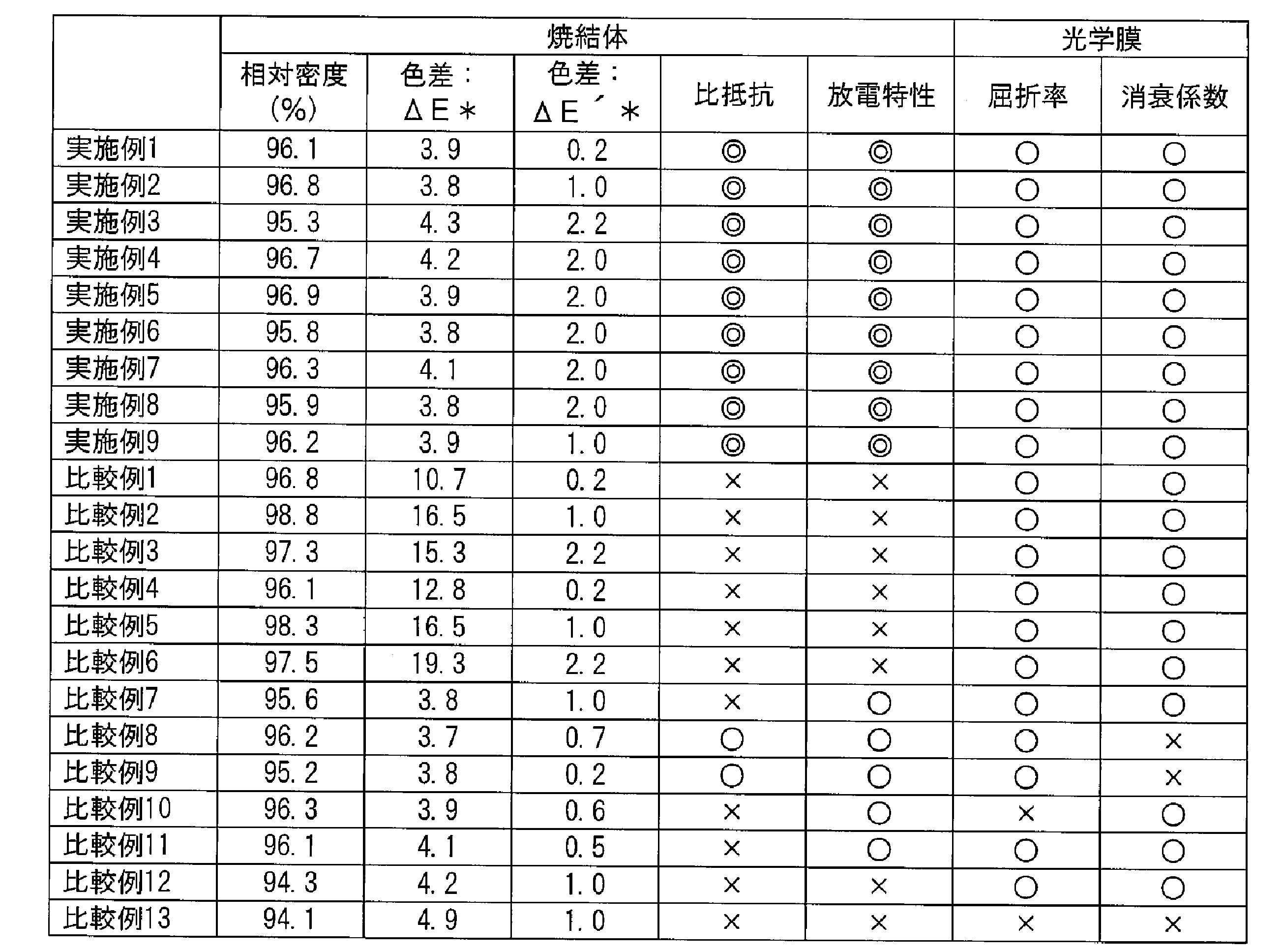
[総合評価]
表1および表2より、本発明の範囲に属する実施例1~9の酸化物焼結体は、いずれも、表面と厚さ方向中心部において、CIE1976空間で測定されるL*a*b*色差:ΔE*が5.0以下、L*a*b*色差:ΔE´*が5.0以下、比抵抗が1×10⁵Ω・cm以下、かつ、相対密度が95.0%以上であることが確認された。また、これらの酸化物焼結体をターゲットして直流スパッタリング法により成膜した場合には、放電時にアーキングがほとんど発生しないことが確認された。さらに、これらの実施例における光学膜は、屈折率:2.1以上、消衰係数:4.08×10⁻²以下を達成しており、反射防止膜などの用途に適用可能であることが確認された。
表1および表2より、本発明の範囲に属する実施例1~9の酸化物焼結体は、いずれも、表面と厚さ方向中心部において、CIE1976空間で測定されるL*a*b*色差:ΔE*が5.0以下、L*a*b*色差:ΔE´*が5.0以下、比抵抗が1×10⁵Ω・cm以下、かつ、相対密度が95.0%以上であることが確認された。また、これらの酸化物焼結体をターゲットして直流スパッタリング法により成膜した場合には、放電時にアーキングがほとんど発生しないことが確認された。さらに、これらの実施例における光学膜は、屈折率:2.1以上、消衰係数:4.08×10⁻²以下を達成しており、反射防止膜などの用途に適用可能であることが確認された。
これに対して、比較例1~13は、酸化物焼結体の組成、焼成雰囲気、および焼成温度のいずれか1つ以上が本発明の範囲から外れる例である。このため、これらの比較例は、L*a*b*色差:ΔE*、L*a*b*色差:ΔE´*や比抵抗などの値が規定範囲になく、安定的に継続して成膜をすることができなかった
本発明の酸化物焼結体は、色むらが少なく、比抵抗の均一性に優れ、かつ、高い相対密度を備える。このため、この酸化物焼結体をターゲットとして用いることで、アーキングなどをほとんど発生させずに、直流スパッタリング法により、高い屈折率を有し、かつ、可視域短波長側における消衰係数が低い光学膜を成膜することが可能となる。このような光学膜は、反射防止膜や機能性多層膜(光学膜)の屈折率制御に用いられる高屈折率膜として、広く適用される。
Claims (6)
- 酸化インジウム、酸化ガリウム、酸化セリウム、ならびに、酸化スズおよび/または酸化チタンを含有する酸化インジウム系酸化物焼結体であって、
前記酸化物焼結体中において、酸化インジウム、酸化ガリウム、酸化セリウム、酸化スズおよび酸化チタンの合計含有量が、98.5モル%以上であり、
前記酸化物焼結体中の、In、GaおよびCeの原子数の合計に対する、
(a)Inの原子数の比:In/(In+Ga+Ce)が0.30~0.54、
(b)Gaの原子数の比:Ga/(In+Ga+Ce)が0.30~0.52、
(c)Ceの原子数の比:Ce/(In+Ga+Ce)が0.16~0.32、
であり、
前記酸化物焼結体中の、In、Ga、Ce、Sn、およびTiの原子数の合計に対する、
(d)Snの原子数の比:Sn/(In+Ga+Ce+Sn+Ti)が0.04以下、
(e)Tiの原子数の比:Ti/(In+Ga+Ce+Sn+Ti)が0.01以下、
であり、かつ、
前記酸化物焼結体の表面と厚さ方向中心位置との間において、CIE1976空間で測定されるL*a*b*色差:ΔE*が5.0以下である、
酸化インジウム系酸化物焼結体。 - 前記酸化物焼結体の表面の径方向中央部と周辺部との間における、CIE1976空間で測定されるL*a*b*色差:ΔE´*が、5.0以下である、請求項1に記載の酸化インジウム系酸化物焼結体。
- 前記酸化物焼結体の表面と厚さ方向中心位置における比抵抗が、いずれも1×10⁵Ω・cm以下である、請求項1または2に記載の酸化インジウム系酸化物焼結体。
- 相対密度が95.0%以上である、請求項1~3のいずれかに記載の酸化インジウム系酸化物焼結体。
- 請求項1~4のいずれかに記載の酸化インジウム系酸化物焼結体の製造方法であって、
酸化インジウム粉末、酸化ガリウム粉末、酸化セリウム粉末、ならびに、酸化スズ粉末および/または酸化チタン粉末を前記組成比となるように粉砕混合し、混合スラリーを得る混合工程と、
前記混合スラリーを噴霧乾燥し、造粒粉末を得る造粒工程と、
前記造粒粉末を加圧成形し、成形体を得る成形工程と、
前記成形体を、不活性ガス雰囲気下で焼成し、酸化物焼結体を得る焼成工程と、
を備える、酸化インジウム系酸化物焼結体の製造方法。 - 請求項1~4のいずれかに記載の酸化物焼結体を用いた、酸化インジウム系スパッタリングターゲット。
Priority Applications (1)
| Application Number | Priority Date | Filing Date | Title |
|---|---|---|---|
| JP2016518221A JP5983903B2 (ja) | 2014-08-01 | 2015-07-24 | 酸化インジウム系酸化物焼結体とその製造方法 |
Applications Claiming Priority (2)
| Application Number | Priority Date | Filing Date | Title |
|---|---|---|---|
| JP2014-158007 | 2014-08-01 | ||
| JP2014158007 | 2014-08-01 |
Publications (1)
| Publication Number | Publication Date |
|---|---|
| WO2016017546A1 true WO2016017546A1 (ja) | 2016-02-04 |
Family
ID=55217447
Family Applications (1)
| Application Number | Title | Priority Date | Filing Date |
|---|---|---|---|
| PCT/JP2015/071125 Ceased WO2016017546A1 (ja) | 2014-08-01 | 2015-07-24 | 酸化インジウム系酸化物焼結体とその製造方法 |
Country Status (3)
| Country | Link |
|---|---|
| JP (1) | JP5983903B2 (ja) |
| TW (1) | TWI592383B (ja) |
| WO (1) | WO2016017546A1 (ja) |
Cited By (3)
| Publication number | Priority date | Publication date | Assignee | Title |
|---|---|---|---|---|
| CN111233440A (zh) * | 2020-02-25 | 2020-06-05 | 基迈克材料科技(苏州)有限公司 | ITiO旋转靶材及其制备方法 |
| CN115745575A (zh) * | 2022-11-30 | 2023-03-07 | 长沙壹纳光电材料有限公司 | 一种氧化物复合粉体及其制备方法与应用 |
| CN119751021A (zh) * | 2024-12-12 | 2025-04-04 | 先导薄膜材料(江苏)有限公司 | 一种掺杂金属氧化物锭的制备方法 |
Families Citing this family (2)
| Publication number | Priority date | Publication date | Assignee | Title |
|---|---|---|---|---|
| US11827972B2 (en) | 2021-01-13 | 2023-11-28 | Jx Metals Corporation | IGZO sputtering target |
| CN116813310B (zh) * | 2023-06-01 | 2024-06-07 | 先导薄膜材料(广东)有限公司 | 一种稀土元素掺杂氧化铟锡镓靶材及其制备方法 |
Citations (6)
| Publication number | Priority date | Publication date | Assignee | Title |
|---|---|---|---|---|
| JPH09176841A (ja) * | 1995-12-21 | 1997-07-08 | Toppan Printing Co Ltd | スパッタリングターゲット |
| JPH09259640A (ja) * | 1996-03-25 | 1997-10-03 | Uchitsugu Minami | 透明導電膜 |
| JP2005320192A (ja) * | 2004-05-07 | 2005-11-17 | Sumitomo Metal Mining Co Ltd | 酸化物焼結体、スパッタリングターゲットおよび透明導電性薄膜 |
| JP2010010347A (ja) * | 2008-06-26 | 2010-01-14 | Sumitomo Metal Mining Co Ltd | 薄膜太陽電池 |
| WO2015098060A1 (ja) * | 2013-12-27 | 2015-07-02 | 出光興産株式会社 | 酸化物焼結体、その製造方法及びスパッタリングターゲット |
| JP2015124145A (ja) * | 2013-12-27 | 2015-07-06 | 住友金属鉱山株式会社 | 酸化インジウム系酸化物焼結体およびその製造方法 |
-
2015
- 2015-07-24 JP JP2016518221A patent/JP5983903B2/ja not_active Expired - Fee Related
- 2015-07-24 WO PCT/JP2015/071125 patent/WO2016017546A1/ja not_active Ceased
- 2015-07-30 TW TW104124709A patent/TWI592383B/zh not_active IP Right Cessation
Patent Citations (6)
| Publication number | Priority date | Publication date | Assignee | Title |
|---|---|---|---|---|
| JPH09176841A (ja) * | 1995-12-21 | 1997-07-08 | Toppan Printing Co Ltd | スパッタリングターゲット |
| JPH09259640A (ja) * | 1996-03-25 | 1997-10-03 | Uchitsugu Minami | 透明導電膜 |
| JP2005320192A (ja) * | 2004-05-07 | 2005-11-17 | Sumitomo Metal Mining Co Ltd | 酸化物焼結体、スパッタリングターゲットおよび透明導電性薄膜 |
| JP2010010347A (ja) * | 2008-06-26 | 2010-01-14 | Sumitomo Metal Mining Co Ltd | 薄膜太陽電池 |
| WO2015098060A1 (ja) * | 2013-12-27 | 2015-07-02 | 出光興産株式会社 | 酸化物焼結体、その製造方法及びスパッタリングターゲット |
| JP2015124145A (ja) * | 2013-12-27 | 2015-07-06 | 住友金属鉱山株式会社 | 酸化インジウム系酸化物焼結体およびその製造方法 |
Cited By (4)
| Publication number | Priority date | Publication date | Assignee | Title |
|---|---|---|---|---|
| CN111233440A (zh) * | 2020-02-25 | 2020-06-05 | 基迈克材料科技(苏州)有限公司 | ITiO旋转靶材及其制备方法 |
| CN115745575A (zh) * | 2022-11-30 | 2023-03-07 | 长沙壹纳光电材料有限公司 | 一种氧化物复合粉体及其制备方法与应用 |
| CN115745575B (zh) * | 2022-11-30 | 2023-09-26 | 长沙壹纳光电材料有限公司 | 一种氧化物复合粉体及其制备方法与应用 |
| CN119751021A (zh) * | 2024-12-12 | 2025-04-04 | 先导薄膜材料(江苏)有限公司 | 一种掺杂金属氧化物锭的制备方法 |
Also Published As
| Publication number | Publication date |
|---|---|
| JP5983903B2 (ja) | 2016-09-06 |
| JPWO2016017546A1 (ja) | 2017-04-27 |
| TWI592383B (zh) | 2017-07-21 |
| TW201634423A (zh) | 2016-10-01 |
Similar Documents
| Publication | Publication Date | Title |
|---|---|---|
| KR101646488B1 (ko) | 산화물 소결물체와 그 제조 방법, 타겟, 및 그것을 이용해 얻어지는 투명 도전막 및 투명 도전성 기재 | |
| JP5983903B2 (ja) | 酸化インジウム系酸化物焼結体とその製造方法 | |
| JP5170009B2 (ja) | 酸化インジウム系スパッタリングターゲットおよびその製造方法 | |
| CN108349816B (zh) | Sn-Zn-O系氧化物烧结体及其制造方法 | |
| TW201609603A (zh) | 氧化物燒結體、濺鍍靶及薄膜以及氧化物燒結體的製造方法 | |
| CN107207356B (zh) | 氧化物烧结体、氧化物溅射靶和氧化物薄膜 | |
| CN104520467B (zh) | 复合氧化物烧结体及氧化物透明导电膜 | |
| JP6064895B2 (ja) | 酸化インジウム系酸化物焼結体およびその製造方法 | |
| US11377725B2 (en) | Oxide sintered body and transparent conductive oxide film | |
| JP7086080B2 (ja) | 酸化物焼結体およびスパッタリングターゲット | |
| JP2015160760A (ja) | 酸化物焼結体及び酸化物透明導電膜 | |
| KR20160133429A (ko) | 산화물 소결체 및 산화물 투명 도전막 | |
| KR20180116293A (ko) | Sn-Zn-O 계 산화물 소결체와 그 제조 방법 | |
| JP6155919B2 (ja) | 複合酸化物焼結体及び酸化物透明導電膜 | |
| WO2015020029A1 (ja) | スパッタリングターゲット及びその製造方法 | |
| JP5754093B2 (ja) | 酸化亜鉛焼結体、その製造方法、スパッタリングターゲット及び透明性膜の製造方法 | |
| WO2017149882A1 (ja) | Sn-Zn-O系酸化物焼結体とその製造方法 | |
| TW201522689A (zh) | 濺鍍靶及其製造方法 | |
| TWI746519B (zh) | 氧化物燒結體、濺鍍靶材以及氧化物透明導電膜及其製造方法 | |
| TW201544612A (zh) | 氧化物燒結體及其製造方法、以及氧化物膜 | |
| JP6280737B2 (ja) | ZnOターゲット材及び透明導電膜の製造方法 | |
| WO2017086016A1 (ja) | Sn-Zn-O系酸化物焼結体とその製造方法 | |
| WO2013042747A1 (ja) | 酸化物焼結体およびその製造方法並びに酸化物透明導電膜 | |
| JP2015024927A (ja) | 酸化物焼結体及びその製造方法、並びに酸化物膜 |
Legal Events
| Date | Code | Title | Description |
|---|---|---|---|
| 121 | Ep: the epo has been informed by wipo that ep was designated in this application |
Ref document number: 15826812 Country of ref document: EP Kind code of ref document: A1 |
|
| ENP | Entry into the national phase |
Ref document number: 2016518221 Country of ref document: JP Kind code of ref document: A |
|
| NENP | Non-entry into the national phase |
Ref country code: DE |
|
| 122 | Ep: pct application non-entry in european phase |
Ref document number: 15826812 Country of ref document: EP Kind code of ref document: A1 |