WO2016013396A1 - 静電保護素子および静電保護回路 - Google Patents
静電保護素子および静電保護回路 Download PDFInfo
- Publication number
- WO2016013396A1 WO2016013396A1 PCT/JP2015/069623 JP2015069623W WO2016013396A1 WO 2016013396 A1 WO2016013396 A1 WO 2016013396A1 JP 2015069623 W JP2015069623 W JP 2015069623W WO 2016013396 A1 WO2016013396 A1 WO 2016013396A1
- Authority
- WO
- WIPO (PCT)
- Prior art keywords
- impurity diffusion
- type impurity
- conductivity type
- electrostatic protection
- diffusion layer
- Prior art date
- Legal status (The legal status is an assumption and is not a legal conclusion. Google has not performed a legal analysis and makes no representation as to the accuracy of the status listed.)
- Ceased
Links
Images









Classifications
-
- H—ELECTRICITY
- H10—SEMICONDUCTOR DEVICES; ELECTRIC SOLID-STATE DEVICES NOT OTHERWISE PROVIDED FOR
- H10D—INORGANIC ELECTRIC SEMICONDUCTOR DEVICES
- H10D89/00—Aspects of integrated devices not covered by groups H10D84/00 - H10D88/00
- H10D89/60—Integrated devices comprising arrangements for electrical or thermal protection, e.g. protection circuits against electrostatic discharge [ESD]
-
- H—ELECTRICITY
- H10—SEMICONDUCTOR DEVICES; ELECTRIC SOLID-STATE DEVICES NOT OTHERWISE PROVIDED FOR
- H10D—INORGANIC ELECTRIC SEMICONDUCTOR DEVICES
- H10D12/00—Bipolar devices controlled by the field effect, e.g. insulated-gate bipolar transistors [IGBT]
- H10D12/211—Gated diodes
-
- H—ELECTRICITY
- H10—SEMICONDUCTOR DEVICES; ELECTRIC SOLID-STATE DEVICES NOT OTHERWISE PROVIDED FOR
- H10D—INORGANIC ELECTRIC SEMICONDUCTOR DEVICES
- H10D62/00—Semiconductor bodies, or regions thereof, of devices having potential barriers
- H10D62/10—Shapes, relative sizes or dispositions of the regions of the semiconductor bodies; Shapes of the semiconductor bodies
- H10D62/13—Semiconductor regions connected to electrodes carrying current to be rectified, amplified or switched, e.g. source or drain regions
- H10D62/141—Anode or cathode regions of thyristors; Collector or emitter regions of gated bipolar-mode devices, e.g. of IGBTs
-
- H—ELECTRICITY
- H10—SEMICONDUCTOR DEVICES; ELECTRIC SOLID-STATE DEVICES NOT OTHERWISE PROVIDED FOR
- H10D—INORGANIC ELECTRIC SEMICONDUCTOR DEVICES
- H10D86/00—Integrated devices formed in or on insulating or conducting substrates, e.g. formed in silicon-on-insulator [SOI] substrates or on stainless steel or glass substrates
- H10D86/201—Integrated devices formed in or on insulating or conducting substrates, e.g. formed in silicon-on-insulator [SOI] substrates or on stainless steel or glass substrates the substrates comprising an insulating layer on a semiconductor body, e.g. SOI
-
- H—ELECTRICITY
- H10—SEMICONDUCTOR DEVICES; ELECTRIC SOLID-STATE DEVICES NOT OTHERWISE PROVIDED FOR
- H10D—INORGANIC ELECTRIC SEMICONDUCTOR DEVICES
- H10D89/00—Aspects of integrated devices not covered by groups H10D84/00 - H10D88/00
- H10D89/60—Integrated devices comprising arrangements for electrical or thermal protection, e.g. protection circuits against electrostatic discharge [ESD]
- H10D89/601—Integrated devices comprising arrangements for electrical or thermal protection, e.g. protection circuits against electrostatic discharge [ESD] for devices having insulated gate electrodes, e.g. for IGFETs or IGBTs
- H10D89/811—Integrated devices comprising arrangements for electrical or thermal protection, e.g. protection circuits against electrostatic discharge [ESD] for devices having insulated gate electrodes, e.g. for IGFETs or IGBTs using FETs as protective elements
- H10D89/813—Integrated devices comprising arrangements for electrical or thermal protection, e.g. protection circuits against electrostatic discharge [ESD] for devices having insulated gate electrodes, e.g. for IGFETs or IGBTs using FETs as protective elements specially adapted to provide an electrical current path other than the field-effect induced current path
-
- H—ELECTRICITY
- H10—SEMICONDUCTOR DEVICES; ELECTRIC SOLID-STATE DEVICES NOT OTHERWISE PROVIDED FOR
- H10W—GENERIC PACKAGES, INTERCONNECTIONS, CONNECTORS OR OTHER CONSTRUCTIONAL DETAILS OF DEVICES COVERED BY CLASS H10
- H10W20/00—Interconnections in chips, wafers or substrates
- H10W20/40—Interconnections external to wafers or substrates, e.g. back-end-of-line [BEOL] metallisations or vias connecting to gate electrodes
- H10W20/41—Interconnections external to wafers or substrates, e.g. back-end-of-line [BEOL] metallisations or vias connecting to gate electrodes characterised by their conductive parts
- H10W20/427—Power or ground buses
-
- H—ELECTRICITY
- H10—SEMICONDUCTOR DEVICES; ELECTRIC SOLID-STATE DEVICES NOT OTHERWISE PROVIDED FOR
- H10W—GENERIC PACKAGES, INTERCONNECTIONS, CONNECTORS OR OTHER CONSTRUCTIONAL DETAILS OF DEVICES COVERED BY CLASS H10
- H10W44/00—Electrical arrangements for controlling or matching impedance
- H10W44/20—Electrical arrangements for controlling or matching impedance at high-frequency [HF] or radio frequency [RF]
-
- H—ELECTRICITY
- H10—SEMICONDUCTOR DEVICES; ELECTRIC SOLID-STATE DEVICES NOT OTHERWISE PROVIDED FOR
- H10D—INORGANIC ELECTRIC SEMICONDUCTOR DEVICES
- H10D62/00—Semiconductor bodies, or regions thereof, of devices having potential barriers
- H10D62/10—Shapes, relative sizes or dispositions of the regions of the semiconductor bodies; Shapes of the semiconductor bodies
- H10D62/124—Shapes, relative sizes or dispositions of the regions of semiconductor bodies or of junctions between the regions
- H10D62/126—Top-view geometrical layouts of the regions or the junctions
Definitions
- the present disclosure relates to an electrostatic protection circuit for protecting an electric circuit from an electrostatic discharge phenomenon and an electrostatic protection element used in the electrostatic protection circuit.
- semiconductor integrated circuits are vulnerable to electrostatic discharge and can be easily destroyed.
- One common source of electrostatic discharge is a human body that accumulates static electricity exceeding 2000V, for example. Therefore, if a human being handles an IC package equipped with a semiconductor integrated circuit without taking any static electricity protection measures, a sudden electrostatic discharge occurs, and the physical circuit for each circuit and each element constituting the semiconductor integrated circuit is generated. May cause destruction.
- a resistive path is formed by inserting a diode as an electrostatic protection element, and a path from the semiconductor integrated circuit as a protected circuit to the electrode pad is shunted.
- the method to do is common. By doing so, it is possible to avoid electrostatic discharge from reaching the protected circuit.
- Patent Document 1 For example, a semiconductor integrated circuit described in Patent Document 1 and an electrostatic discharge protection device described in Patent Document 2 have been proposed as attempts to achieve both electrostatic resistance and RF characteristics.
- Patent Document 1 it is difficult to achieve both protection capability and RF characteristics for a protected circuit particularly in a high frequency region. Further, in Patent Document 2, since a control circuit for controlling the potential of the gate electrode is separately provided, it is difficult to reduce the size and simplify, and the generation of league current flowing through the electrostatic protection diode is also a problem. .
- An electrostatic protection element as one embodiment of the present disclosure includes an insulator and a semiconductor layer formed on the insulator.
- the semiconductor layer includes a first first conductivity type impurity diffusion layer, a body region, a second first conductivity type impurity diffusion layer, and a second conductivity type impurity diffusion layer electrically isolated from the body region. It has an element formation region in which conductive type regions are arranged in order, and an element isolation region provided with an element isolation layer surrounding the element formation region.
- a gate electrode provided via an insulating film is further provided on the body region in the semiconductor layer.
- An electrostatic protection circuit as an embodiment of the present disclosure includes an insulator, and an electrostatic protection element and a semiconductor integrated circuit formed on the insulator.
- the electrostatic protection element includes a first first conductivity type impurity diffusion layer, a body region, a second first conductivity type impurity diffusion layer, and a second conductivity type impurity diffusion layer electrically isolated from the body region.
- a semiconductor layer having an element formation region in which the second conductivity type regions are arranged in sequence, and an element isolation region provided with an element isolation layer surrounding the element formation region, and an insulating film provided on the body region A gate electrode.
- the semiconductor integrated circuit is provided in the semiconductor layer.
- the body region when static electricity is applied to the first first-conductivity-type impurity diffusion layer, the body region becomes a channel region and is electrically open. An electrostatic potential is conducted to a certain (that is, floating) second first conductivity type impurity diffusion layer. The junction between the second first-conductivity-type impurity diffusion layer through which the electrostatic potential is conducted and the second-conductivity-type region including the adjacent second-conductivity-type impurity diffusion layer is in a forward bias state.
- a one-stage diode formed of a junction between the second first conductivity type impurity diffusion layer and the second conductivity type region is formed from the first first conductivity type impurity diffusion layer via the channel region (body region).
- an electrostatic discharge operation is performed. That is, in the electrostatic protection element, when static electricity is applied to the first first conductivity type impurity diffusion layer, it functions as a single-stage diode including one PN junction, and electrostatic discharge is performed.
- the junction between the body region that does not become the channel region is also electrically open, the junction between the body region and the first first conductivity type impurity diffusion layer to which the signal potential is applied is in a weak forward bias state.
- the junction between the body region and the second first-conductivity-type impurity diffusion layer is in a weak reverse bias state.
- the junction between the second first-conductivity-type impurity diffusion layer and the second-conductivity-type region at the power supply potential is also in a reverse bias state.
- the second conductivity type region are connected in series. The parasitic capacitance of the electrostatic protection element is sufficiently reduced as compared with the conventional case.
- the electrostatic protection element and the electrostatic protection circuit as one embodiment of the present disclosure, it is possible to exhibit excellent performance in the protection capability, electrostatic resistance, and RF characteristics for the protected circuit.
- the effect of this indication is not limited to this, Any effect of the following description may be sufficient.
- FIG. 1A It is sectional drawing showing the structural example of the electrostatic protection element which concerns on 1st Embodiment of this indication. It is a top view showing the example of a structure of the electrostatic protection element shown to FIG. 1A. It is explanatory drawing showing operation
- FIG. 7 is a cross-sectional view illustrating a configuration of a protection diode applied to the general electrostatic protection circuit illustrated in FIGS. 6A to 6C.
- FIG. 7 is a cross-sectional view illustrating a configuration of a protection diode applied to the general electrostatic protection circuit illustrated in FIGS. 6A to 6C.
- FIG. 6 is a characteristic diagram showing the relationship between frequency and impedance in the electrostatic protection element mounted on the electrostatic protection circuit shown in FIGS. 5A to 5C.
- FIG. 6 is a characteristic diagram showing the relationship between voltage and current in the electrostatic protection element mounted on the electrostatic protection circuit shown in FIGS. 5A to 5C.
- First embodiment positive protection element
- Second embodiment input / output circuit using a positive protection element
- Third embodiment negative protection element
- Third embodiment negative protection element
- Fourth embodiment input / output circuit using a negative protection element
- Fifth embodiment 5-1 Configuration 5-2 Operation when positive static electricity is applied
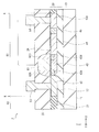
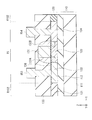
- FIG. 1A shows a cross-sectional configuration of an electrostatic protection element 1 as a first embodiment of the present disclosure.
- FIG. 1B shows a planar configuration of the electrostatic protection element 1.
- FIG. 1A corresponds to a cross-sectional view in the direction of the arrow along the line IA-IA shown in FIG. 1B.
- the electrostatic protection element 1 is used to protect a protected circuit such as a semiconductor integrated circuit from damage due to positive electrostatic discharge.
- the electrostatic protection element 1 has an SOI (Silicon on Insulator) structure.
- SOI Silicon on Insulator
- a semiconductor layer 20 and a gate electrode 31 are sequentially stacked on a base 10.
- the base 10 is obtained by providing a thin buried oxide film 12 made of, for example, a silicon oxide film on a support substrate 11 made of, for example, single crystal silicon.
- the semiconductor layer 20 is a thin film made of, for example, single crystal silicon, and has an element formation region R1 and an element isolation region R2 provided with an element isolation layer 21 surrounding the element formation region R1.
- the element isolation layer 21 is an insulating film made of, for example, a silicon oxide film (SiO 2 ), and is formed using, for example, an STI (Shallow Trench Isolation) technique.
- the element formation region R1 includes a P + anode region 22 as a first first conductivity type impurity diffusion layer, a body region 23, a P + potential transmission region 24 as a second first conductivity type impurity diffusion layer, and a body region 23.
- a part of the body region 23 is provided with a pair of P-type low level doped drains (PLDD) 23A and 23B.
- PLDD P-type low level doped drains
- an insulating film 26 is provided so as to cover the entire cathode region 25 including the P + anode region 22, the body region 23, the P + potential transmission region 24, and the N + cathode region 25A.
- a part of the upper surface of the P + anode region 22 and a part of the upper surface of the N + cathode region 25A are not covered with the insulating film 26 and are connected to the anode electrode 33 and the cathode electrode 34, respectively.
- the gate electrode 31 is provided on the body region 23 via an insulating film 26. Therefore, a part of the insulating film 26 sandwiched between the body region 23 and the gate electrode 31 functions as a gate insulating film. Side wall spacers 32A and 32B are provided on both sides of the gate electrode 31, and the whole is covered with an insulating film 35. In FIG. 1B, the insulating film 26 and the insulating film 35 are not shown.
- the body region 23 is an N well and is surrounded by the P + anode region 22, the P + potential transmission region 24, and the element isolation layer 21 in the stacking plane (in the XY plane). That is, the end surface of the body region 23 is in contact with any one of the P + anode region 22, the P + potential transmission region 24, and the element isolation layer 21.
- the body region 23 is sandwiched between the buried oxide film 12 and the insulating film 26 in the thickness direction (Z-axis direction). That is, the lower surface of the body region 23 is in contact with the buried oxide film 12, and the upper surface of the body region 23 is in contact with the insulating film 26.
- the P + potential transmission region 24 is surrounded by the body region 23, the cathode region 25, and the element isolation layer 21 in the stacking plane (in the XY plane). That is, the end face of the P + potential transmission region 24 is in contact with any of the body region 23, the cathode region 25, and the element isolation layer 21.
- the P + potential transmission region 24 is sandwiched between the buried oxide film 12 and another insulating film such as the insulating film 26 or the insulating film 35 in the thickness direction (Z-axis direction). That is, the lower surface of the P + potential transmission region 24 is in contact with the buried oxide film 12, and the upper surface of the P + potential transmission region 24 is in contact with another insulating film such as the insulating film 26 or the insulating film 35.
- the body region 23 and the P + potential transmission region 24 are isolated from the surroundings and are in an electrically open state, that is, in a floating state.
- the cathode region 25 is electrically isolated from the body region 23 by the P + potential transmission region 24, the buried oxide film 12, and the element isolation layer 21.
- the pair of PLDDs 23A and 23B formed in a part of the body region 23 are positioned so as to face the pair of sidewall spacers 32A and 32B provided with the gate electrode 31 in between.
- the PLDDs 23A and 23B are P-impurity diffusion layers formed by ion implantation of P-type impurities into the body region 23 after the gate electrode 31 is formed, for example.
- the P + anode region 22 and the P + potential transmission region 24 are made of a P + impurity diffusion layer, and are formed together after the side wall spacers 32A and 32B are formed on both sides of the gate electrode 31, respectively.
- the gate electrode 31 and the N + cathode region 25A may be connected to a common wiring, for example, and have a common first potential.
- the P + anode region 22 (anode electrode 33) has a second potential different from the first potential.
- the first potential here is, for example, a power supply potential or a reference potential, and the second potential is a signal potential.
- the electrostatic protection element 1 functions as a positive protection diode. That is, when the gate electrode 31 and the cathode electrode 34 are electrically connected to have the same reference potential and positive static electricity is applied to the anode electrode 33, the electrostatic protection operation is started. Specifically, when positive static electricity is applied to the P + anode region 22 from the outside when the gate electrode 31 is at the reference potential, the body region 23 (N well) immediately below the gate electrode 31 becomes a P + channel layer. . Then, the electrostatic potential is conducted to the P + potential transmission region 24 that is electrically open through the body region 23 that has become the P + channel layer.
- the junction between the P + potential transmission region 24 through which the electrostatic potential is conducted and the cathode region 25 that is the reference potential is in a forward bias state. Therefore, electrostatic discharge is performed sequentially from the P + anode region 22 to the body region 23 which is the P + channel layer, the junction between the P + potential transmission region 24 and the cathode region 25, the N + cathode region 25A, and the cathode electrode 34.
- the electrostatic protection element 1 functions as a one-stage electrostatic protection diode including one PN junction.
- the electrostatic protection element 1 Refers to movement.
- the anode electrode 33 becomes the signal potential when the cathode electrode 34 and the gate electrode 31 are at the power supply potential
- the P + anode region 22 also becomes the signal potential, so that the body region 23 (N well) immediately below the gate electrode 31 becomes a channel region. Must not. This is because the signal potential is lower than the power supply potential.
- the P + potential transmission region 24 is electrically opened.
- the body region 23 is also electrically open.
- the junction between P + anode region 22 and body region 23 is in a weak forward bias state, and the junction between body region 23 and P + potential transmission region 24 is in a weak reverse bias state.
- the junction between the P + potential transmission region 24 and the power supply potential N + cathode region 25A is also in a reverse bias state.
- the electrostatic protection element 1 enters an off state that does not function as a positive protection diode.
- the electrostatic protection element 1 in the off state includes the first junction between the P + anode region 22 and the body region 23, the second junction between the body region 23 and the P + potential transmission region 24, and the P + potential transmission.
- the third junction between the region 24 and the cathode region 25 is connected in series.
- the parasitic capacitance between the anode electrode 33 and the cathode electrode 34 can be reduced to about 1/3 compared with the general gate diode structure shown in FIG. 8, for example.
- the electrostatic protection element 1 behaves as a single-stage electrostatic protection diode including one PN junction when static electricity is applied, it is compared with a case where three PN junctions are simply connected in series. Thus, the electrostatic protection operation is performed at a voltage of about 1/3.
- the electrostatic protection element 1 of the present embodiment when positive static electricity is applied, it functions as a single-stage electrostatic protection diode that performs electrostatic discharge through an appropriate path, and other normal In operation, it functions as a diode including three stages of PN junctions connected in series. Therefore, by reducing the parasitic capacitance during normal operation while securing a high protection capability from electrostatic discharge, it is possible to suppress a decrease in impedance particularly in a high-frequency signal and to exhibit high isolation characteristics. Further, since the electrostatic protection element 1 has a simple configuration, it can be easily manufactured by the same procedure as that of a general PMOS transistor.
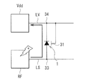
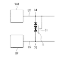
- FIGS. 2A and 2B show an example of an input / output circuit using the electrostatic protection element 1 described above.
- the input / output circuits shown in FIGS. 2A and 2B constitute a part of a semiconductor integrated circuit (not shown) which is a protected circuit.
- FIG. 2A explains the configuration of the input / output circuit using the electrostatic protection element 1 and the electrostatic protection operation of the electrostatic protection element 1 when positive static electricity is applied to the input / output circuit. is there.
- FIG. 2B illustrates the configuration of the input / output circuit using the electrostatic protection element 1 and the state of the electrostatic protection element 1 when the semiconductor integrated circuit including the input / output circuit is operating normally. It is.
- the cathode electrode 34 and the gate electrode 31 of the electrostatic protection element 1 are connected to the power supply potential line LV, and the anode electrode 33 of the electrostatic protection element 1 is connected to the signal potential line LS.
- a pad Vdd for applying power to the semiconductor integrated circuit is connected to the power supply potential line LV, and a pad RF for supplying input / output signals of the semiconductor integrated circuit is connected to the signal potential line LS.
- the junction between the P + potential transmission region 24 through which the electrostatic potential is conducted and the cathode region 25 that is the reference potential is in a forward bias state. For this reason, the electrostatic discharge sequentially passes from the P + anode region 22 to the body region 23 which is the P + channel layer, the junction between the P + potential transmission region 24 and the cathode region 25, the N + cathode region 25A, and the cathode electrode 34.
- the power supply potential line LV which is a reference potential.
- the electrostatic protection element 1 functions as a one-stage electrostatic protection diode including one PN junction.
- a power supply potential is applied to pad Vdd and a signal potential is applied to pad RF.
- a power supply potential is applied to the cathode electrode 34 and the gate electrode 31 via the power supply potential line LV, and the anode electrode 33 becomes a signal potential from the pad RF via the signal potential line LS. Therefore, since the P + anode region 22 also has a signal potential, the body region 23 (N well) immediately below the gate electrode 31 does not become a channel region. This is because the signal potential is lower than the power supply potential. Therefore, the P + potential transmission region 24 is electrically opened.
- the body region 23 is also electrically open. Therefore, the junction between P + anode region 22 and body region 23 (N well) is in a weak forward bias state, and the junction between body region 23 (N well) and P + potential transmission region 24 is in a weak reverse bias state. Further, the junction between the P + potential transmission region 24 and the cathode region 25 which is the power supply potential is also in a reverse bias state. As a result, the electrostatic protection element 1 enters an off state that does not function as a positive protection diode. As described above, the electrostatic protection element 1 in the off state includes the first junction between the P + anode region 22 and the body region 23, the second junction between the body region 23 and the P + potential transmission region 24, and the P + potential transmission.
- the third junction between the region 24 and the cathode region 25 is connected in series. For this reason, the parasitic capacitance between the anode electrode 33 and the cathode electrode 34 can be reduced to about 1/3 compared with the general gate diode structure shown in FIG. 8, for example.
- the input / output circuit including the electrostatic protection element 1 of the present embodiment when positive static electricity is applied, it functions as a one-stage electrostatic protection diode that performs electrostatic discharge through an appropriate path. In other normal operations, it functions as a diode including three stages of PN junctions connected in series. Therefore, by reducing the parasitic capacitance during normal operation while securing a high protection capability from electrostatic discharge, it is possible to suppress a decrease in impedance particularly in a high-frequency signal and to exhibit high isolation characteristics.
- FIG. 3 illustrates a cross-sectional configuration of the electrostatic protection element 2 according to the third embodiment of the present disclosure.
- the electrostatic protection element 2 is used to protect a protected circuit such as a semiconductor integrated circuit from damage due to negative electrostatic discharge.
- the following description will focus on differences from the electrostatic protection element 1 described in the first embodiment, and the same components as those in the electrostatic protection element 1 will be denoted by the same reference numerals and description thereof will be omitted as appropriate. .
- the element formation region R1 in the electrostatic protection element 2 includes an N + cathode region 42 as a first first conductivity type impurity diffusion layer, a body region 43 as a P well, and a second first conductivity type impurity diffusion layer.
- An N + potential transmission region 44 and an anode region 45 including a P + anode region 45 as a second conductivity type impurity diffusion layer electrically isolated from the body region 43 are arranged in order.
- a part of the body region 43 is provided with a pair of N-type low level doped drains (NLDD) 43A and 43B.
- an insulating film 26 is provided so as to cover the entire anode region 45 including the N + cathode region 42, the body region 43, the N + potential transmission region 44, and the P + anode region 45A.
- a part of the upper surface of the N + cathode region 42 and a part of the upper surface of the P + anode region 45A are not covered with the insulating film 26 and are connected to the cathode electrode 53 and the anode electrode 54, respectively.
- the electrostatic protection element 2 further includes a gate electrode 61.
- the gate electrode 61 is provided on the body region 43 via the insulating film 26. Therefore, a part of the insulating film 26 sandwiched between the body region 43 and the gate electrode 61 functions as a gate insulating film.
- Side wall spacers 62A and 62B are provided on both sides of the gate electrode 61, and the insulating film 35 covers the whole.
- the body region 43 is a P-well, and is surrounded by the N + cathode region 42, the N + potential transmission region 44, and the element isolation layer 21 in the stacking plane (in the XY plane). That is, the end surface of the body region 43 is in contact with any one of the N + cathode region 42, the N + potential transmission region 44, and the element isolation layer 21.
- the body region 43 is sandwiched between the buried oxide film 12 and the insulating film 26 in the thickness direction (Z-axis direction). That is, the lower surface of the body region 43 is in contact with the buried oxide film 12, and the upper surface of the body region 43 is in contact with the insulating film 26.
- the N + potential transmission region 44 is surrounded by the body region 43, the anode region 45, and the element isolation layer 21 in the stacking plane (in the XY plane). That is, the end surface of the N + potential transmission region 44 is in contact with any of the body region 43, the anode region 45, and the element isolation layer 21.
- the N + potential transmission region 44 is sandwiched between the buried oxide film 12 and the insulating film 26 in the thickness direction (Z-axis direction). That is, the lower surface of the N + potential transmission region 44 is in contact with the buried oxide film 12, and the upper surface of the N + potential transmission region 44 is in contact with the insulating film 26.
- the body region 43 and the N + potential transmission region 44 are isolated from the surroundings and are in an electrically open state, that is, in a floating state.
- the anode region 45 is electrically isolated from the body region 43 by the N + potential transmission region 44, the buried oxide film 12, and the element isolation layer 21.
- the pair of NLDDs 43A and 43B formed in a part of the body region 43 are positioned so as to face the pair of sidewall spacers 62A and 62B provided with the gate electrode 61 interposed therebetween.
- the NLDDs 43A and 43B are N ⁇ impurity diffusion layers formed by ion implantation of N-type impurities into the body region 43 after the gate electrode 61 is formed, for example.
- the N + cathode region 42 and the N + potential transmission region 44 are made of an N + impurity diffusion layer, and are formed after the side wall spacers 62A and 62B are formed on both sides of the gate electrode 61, respectively.
- the gate electrode 61 and the P + anode region 45A may be connected to a common wiring, for example, and have a common first potential.
- the N + cathode region 42 (cathode electrode 53) has a second potential different from the first potential.
- the first potential here is, for example, a power supply potential or a reference potential, and the second potential is a signal potential.
- the electrostatic protection element 2 functions as a negative protection diode. That is, when the gate electrode 61 and the anode electrode 54 are electrically connected to have the same reference potential and negative static electricity is applied to the cathode electrode 53, the electrostatic protection operation is started. Specifically, when negative static electricity is applied to the N + cathode region 42 from the outside when the gate electrode 61 is at the reference potential, the body region 43 (P well) immediately below the gate electrode 61 becomes an N + channel layer. . Then, the electrostatic potential is conducted to the N + potential transmission region 44 that is electrically open through the body region 43 that becomes the N + channel layer.
- the junction between the N + potential transmission region 44 through which the electrostatic potential is conducted and the anode region 45 as the reference potential is in a forward bias state. For this reason, electrostatic discharge is performed sequentially from the N + cathode region 42 to the body region 43 that is the N + channel layer, the junction between the N + potential transmission region 44 and the anode region 45, the P + anode region 45A, and the anode electrode 54.
- the electrostatic protection element 2 functions as a one-stage electrostatic protection diode including one PN junction.
- the operation of the electrostatic protection element 2 in the off state where the electrostatic protection element 2 does not function as a negative protection diode will be described. That is, the operation of the electrostatic protection element 2 after electrostatic discharge is performed or when each potential of the anode electrode 54 and the cathode electrode 53 is applied so that the electrostatic protection element 2 does not function as a negative protection diode.
- the cathode electrode 53 becomes the signal potential when the anode electrode 54 and the gate electrode 61 are at the reference potential
- the N + cathode region 42 also becomes the signal potential, so that the body region 43 (P well) immediately below the gate electrode 61 becomes a channel region. Must not. This is because the signal potential is higher than the reference potential.
- the N + potential transmission region 44 is electrically opened.
- the body region 43 is also electrically open. Therefore, the junction between N + cathode region 42 and body region 43 is in a reverse bias state, and the junction between body region 43 and N + potential transmission region 44 is in a weak forward bias state. Furthermore, the junction between the N + potential transmission region 44 and the anode region 45 that is the reference potential is in a reverse bias state. As a result, the electrostatic protection element 2 enters an off state that does not function as a negative protection diode.
- the electrostatic protection element 2 in the off state includes the first junction between the N + cathode region 42 and the body region 43, the second junction between the body region 43 and the N + potential transmission region 44, and N + potential transmission.
- the third junction between the region 44 and the anode region 45 is connected in series. For this reason, the parasitic capacitance between the cathode electrode 53 and the anode electrode 54 can be reduced to about 1/3 compared with the general gate diode structure shown in FIG. 8, for example.
- the electrostatic protection element 2 of the present embodiment when negative static electricity is applied, it functions as a single-stage electrostatic protection diode that performs electrostatic discharge through an appropriate path, and other normal In operation, it functions as a diode including three stages of PN junctions connected in series. Therefore, by reducing the parasitic capacitance during normal operation while securing a high protection capability from electrostatic discharge, it is possible to suppress a decrease in impedance particularly in a high-frequency signal and to exhibit high isolation characteristics.
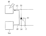
- FIGS. 4A and 4B show an example of an input / output circuit using the electrostatic protection element 2 described above.
- the input / output circuits shown in FIGS. 4A and 4B constitute a part of a semiconductor integrated circuit (not shown) which is a protected circuit.
- FIG. 4A explains the configuration of the input / output circuit using the electrostatic protection element 2 and the electrostatic protection operation of the electrostatic protection element 2 when negative static electricity is applied to the input / output circuit. is there.
- FIG. 4B illustrates the configuration of the input / output circuit using the electrostatic protection element 2 and the state of the electrostatic protection element 2 when the semiconductor integrated circuit including the input / output circuit is operating normally. It is.
- the anode electrode 54 and the gate electrode 61 of the electrostatic protection element 2 are connected to the reference potential line LR, and the cathode electrode 53 of the electrostatic protection element 2 is connected to the signal potential line LS.
- a pad Vss for grounding the semiconductor integrated circuit is connected to the reference potential line LR, and a pad RF for supplying input / output signals of the semiconductor integrated circuit is connected to the signal potential line LS.
- the junction between the N + potential transmission region 44 through which the electrostatic potential is conducted and the anode region 45 as the reference potential is in a forward bias state. For this reason, electrostatic discharge sequentially passes from the P + anode region 45A to the junction between the anode region 45 and the N + potential transmission region 44, the body region 43, which is the N + channel layer, the N + cathode region 42, and the cathode electrode 53.
- the signal potential line LS which is a signal potential.
- the electrostatic protection element 2 functions as a one-stage electrostatic protection diode including one PN junction.
- the junction between N + cathode region 42 and body region 43 (P well) is in a reverse bias state, and the junction between body region 43 (P well) and N + potential transmission region 44 is in a weak forward bias state. Furthermore, the junction between the N + potential transmission region 44 and the anode region 45 that is the reference potential is in a reverse bias state.
- the electrostatic protection element 2 enters an off state that does not function as a negative protection diode.
- the electrostatic protection element 2 in the off state includes the first junction between the N + cathode region 42 and the body region 43, the second junction between the body region 43 and the N + potential transmission region 44, and N + potential transmission.
- the third junction between the region 44 and the anode region 45 is connected in series. For this reason, the parasitic capacitance between the cathode electrode 53 and the anode electrode 54 can be reduced to about 1/3 compared with the general gate diode structure shown in FIG. 8, for example.
- the input / output circuit including the electrostatic protection element 2 of the present embodiment when negative static electricity is applied, it functions as a one-stage electrostatic protection diode that performs electrostatic discharge through an appropriate path. In other normal operations, it functions as a diode including three stages of PN junctions connected in series. Therefore, by reducing the parasitic capacitance during normal operation while securing a high protection capability from electrostatic discharge, it is possible to suppress a decrease in impedance particularly in a high-frequency signal and to exhibit high isolation characteristics.
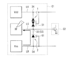
- FIGS. 5A to 5C show an example of an electrostatic protection circuit including an input / output circuit including the electrostatic protection element 1 and the electrostatic protection element 2 described above.
- the electrostatic protection circuit shown in FIGS. 5A to 5C includes, for example, an input / output circuit C1 including the electrostatic protection element 1 and the electrostatic protection element 2 on the same substrate 10, and a semiconductor integrated circuit C2 which is a protected circuit. (Internal circuit).
- FIG. 5A illustrates the configuration of the electrostatic protection circuit of the present embodiment and the electrostatic protection operation when positive static electricity is applied to the input / output circuit C1.
- FIG. 5B also explains the configuration of the electrostatic protection circuit of the present embodiment and the electrostatic protection operation when negative static electricity is applied to the input / output circuit C1.
- FIG. 5C explains the configuration of the electrostatic protection circuit of the present embodiment and the state of the electrostatic protection elements 1 and 2 when the semiconductor integrated circuit C2 is operating normally.
- the anode electrode 54 and the gate electrode 61 of the electrostatic protection element 2 described in the third embodiment are further connected to the reference potential line LR, and the cathode electrode 53 of the electrostatic protection element 2 is used. Is connected to the signal potential line LS. A pad Vss for grounding the semiconductor integrated circuit C2 is connected to the reference potential line LR.
- the semiconductor integrated circuit C2 is connected to, for example, the end of the signal potential line LS in the input / output circuit C1 opposite to the pad RF.
- electrostatic protection circuit In this electrostatic protection circuit, when the pad Vdd is grounded and the power supply potential line LV is set as a reference potential, and positive static electricity based on the potential is applied to the pad RF, the electrostatic protection element 1 is applied to the semiconductor integrated circuit C2. The electrostatic protection operation is started (FIG. 5A). This electrostatic protection operation against positive static electricity is as described in the first and second embodiments.
- the electrostatic protection element 1 functions as a one-stage electrostatic protection diode by joining the P + potential transmission region 24 and the cathode region 25.
- the electrostatic protection element 2 when electrostatic discharge is performed by the electrostatic protection element 1 against positive static electricity, one of the electrostatic protection elements 2 is in the off state described in the third and fourth embodiments. ing. Therefore, when the pad Vss is grounded, the reference potential line LR is set to the reference potential, and negative static electricity based on the reference potential line LR is applied to the pad RF, the electrostatic protection element 2 performs the electrostatic protection operation on the semiconductor integrated circuit C2. Start (FIG. 5B). The electrostatic protection operation against the negative static electricity is as described in the third and fourth embodiments.
- the electrostatic protection element 2 functions as a one-stage electrostatic protection diode formed by joining the N + potential transmission region 44 and the anode region 45. Thus, when electrostatic discharge is performed by the electrostatic protection element 2 against negative static electricity, one of the electrostatic protection elements 1 is in the off state described in the first and second embodiments. ing.
- the electrostatic protection circuit includes the electrostatic protection element 1 and the electrostatic protection element 2, thereby appropriately protecting the semiconductor integrated circuit C ⁇ b> 2 when both positive static electricity and negative static electricity are applied. The operation is performed.
- both the electrostatic protection element 1 and the electrostatic protection element 2 are in the off state (FIG. 5C). That is, the electrostatic protection element 1 is in the off state described in the first and second embodiments, and the electrostatic protection element 2 is in the off state described in the third and fourth embodiments. Yes. Therefore, during normal operation, each of the electrostatic protection element 1 and the electrostatic protection element 2 functions as a diode including three stages of PN junctions connected in series.
- the electrostatic protection element 1 and the electrostatic protection element 2 can suppress a decrease in impedance particularly in a high-frequency signal by reducing their own parasitic capacitance, and can exhibit high isolation characteristics.
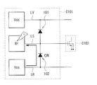
- [General electrostatic protection circuit] 6A to 6C show examples of an electrostatic protection operation by a general electrostatic protection circuit using a diode as an electrostatic protection element.
- a general electrostatic protection circuit including an input / output circuit C101 and a semiconductor integrated circuit C102 is considered.
- a positive protection diode 101 is inserted between the power supply potential line LV and the signal potential line LS, and its anode terminal is connected to the signal potential line LS and its cathode terminal is connected to the power supply potential line LV.
- a negative protection diode 102 is inserted between the signal potential line LS and the reference potential line LR, its anode terminal is connected to the reference potential line LR, and its cathode terminal is connected to the signal potential line LS.
- a pad RF is connected to one end, and a semiconductor integrated circuit C102 is connected to the other end.
- the allowable value of the parasitic capacitance of the protection diode is determined from the viewpoint of whether leakage of high-frequency signals can be prevented (whether isolation can be performed). This is because the higher the frequency of the signal to be handled and the greater the parasitic capacitance of the protection diode, the lower the impedance and the isolation performance deteriorates.
- the parasitic capacitance is reduced by reducing the size of the protection diode so that the RF characteristics are not sacrificed.
- the electrostatic resistance is reduced and the protection capability for the internal circuit is reduced. Compatibility with RF characteristics becomes difficult.
- Patent Document 1 described above, an attempt is made to solve such a problem of achieving both electrostatic resistance and RF characteristics.
- a multistage positive protection diode 101n and a multistage negative protection diode 102n are connected in series.
- the protection diode can be regarded as a capacitor.
- the capacitance can be reduced by connecting a plurality of protective diodes in series in multiple stages, and in particular, a reduction in impedance in a high-frequency signal can be suppressed and the isolation characteristics can be improved.
- FIG. 8 is a cross-sectional view of a general so-called gated diode using an SOI substrate.
- a gated diode is formed in the semiconductor layer surrounded by the element isolation region.
- a semiconductor layer 120 is provided on a base 110 on which a buried oxide film 112 is formed on a support substrate 111.
- an N + impurity diffusion layer 122, a body region 123, and a P + impurity diffusion layer 124 are sequentially arranged in the in-plane direction.
- An element isolation layer 121 is provided in the element isolation region R102 surrounding the element formation region R101.
- a gate electrode 131 is formed on the body region 123 with an insulating film 126 formed so as to cover a part of the semiconductor layer 120.
- the protection diode shown in FIG. 8 is used as the positive protection diode in the electrostatic protection circuit of FIGS. 6A to 6C and FIG. 7, the P + impurity diffusion layer 124 is connected to the signal potential line LS and the N + impurity diffusion layer 122 is connected to the power supply potential. Connect to line LV.
- the gate electrode 131 is connected to the signal potential line LS or the power supply potential line LV.
- the protection diode shown in FIG. 8 is used as the negative protection diode in the electrostatic protection circuits of FIGS. 6A to 6C and FIG. 7, the P + impurity diffusion layer 124 is connected to the reference potential line LR, and the N + impurity diffusion layer 122 is Connect to signal potential line LS.
- the gate electrode 131 is connected to the reference potential line LR or the signal potential line LS.
- the reference potential line LR is used as a reference potential and negative static electricity based on the reference potential is applied to the signal potential line LS, the body region 123 and the N + impurity diffusion layer in the negative protection diode
- the junction with 122 is forward-biased, and the positive protection diode operates in the forward direction to cause electrostatic discharge.
- Patent Document 2 described above, an attempt is made to solve the problem of coexistence of the ability to protect internal elements and RF characteristics.
- Patent Document 2 since the electrostatic protection diode between the potential line to be protected and the reference potential line is connected in the forward direction, it is considered that an increase in leakage current in IC operation is inevitable.
- the electrostatic protection elements 1 and 2 function as a one-stage protection diode during an electrostatic protection operation, and function as a three-stage protection diode to which a reverse bias is applied during a normal operation of the semiconductor integrated circuit C2. is there.
- the parasitic capacitance between the anode and the cathode is about 1/8 compared to the general protection diode shown in FIG. 8.
- the isolation characteristic for the RF signal is about three times or the impedance is about three times.
- the horizontal axis indicates the RF frequency
- the vertical axis indicates the impedance.
- the symbol ⁇ in the figure indicates the characteristics of the electrostatic protection elements 1 and 2 of the present disclosure
- the symbol ⁇ in the figure indicates the characteristics of the general protection diode shown in FIG. 8.
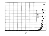
- the electrostatic protection elements 1 and 2 of the present disclosure have a parasitic capacitance equivalent to that of the general protection diode illustrated in FIG. 8, for example, the electrostatic protection elements 1 and 2 of the present disclosure as illustrated in FIG. 10.
- the current capability is about three times that of a general protection diode.
- the horizontal axis indicates the voltage Vf
- the vertical axis indicates the current If.
- the symbol ⁇ in the figure indicates the characteristics of the electrostatic protection elements 1 and 2 of the present disclosure
- the symbol ⁇ in the figure indicates the characteristics of the general protection diode shown in FIG. 8. For this reason, both RF characteristics and static electricity resistance are realized.
- the electrostatic protection element has the SOI structure, but the present technology is not limited to this.
- the electrostatic protection element is SOS (Silicon -On-sapphire) structure.
- a sapphire substrate may be used instead of the support substrate 11 and the buried oxide film 12.
- this technique can take the following structures.
- An insulator A first conductivity type impurity diffusion layer formed on the insulator, a body region, a second first conductivity type impurity diffusion layer, and a second conductivity type impurity diffusion electrically isolated from the body region;
- a semiconductor layer having an element formation region in which second conductivity type regions including layers are sequentially arranged, and an element isolation region provided with an element isolation layer surrounding the element formation region;
- An electrostatic protection element comprising: a gate electrode provided on the body region via an insulating film.
- the gate electrode and the second conductivity type impurity diffusion layer have a common first potential, The electrostatic protection element according to (1), wherein the first first conductivity type impurity diffusion layer has a second potential.
- the first potential is a power supply potential or a reference potential;
- the body region is Surrounded by the first first conductivity type impurity diffusion layer, the second first conductivity type impurity diffusion layer, and the element isolation layer in an in-plane direction;
- the second first conductivity type impurity diffusion layer includes: Surrounded by the body region, the second conductivity type region and the element isolation layer in an in-plane direction; The electrostatic protection element according to any one of (1) to (4), wherein the electrostatic protection element is sandwiched between the insulator and the insulating film or another insulating film in a thickness direction.
- the first and second first-conductivity-type impurity diffusion layers are both P-type impurity diffusion layers, The electrostatic protection element according to any one of (1) to (5), wherein the second conductivity type impurity diffusion layer is an N-type impurity diffusion layer.
- the gate electrode and the second conductivity type impurity diffusion layer have a common power supply potential, The electrostatic protection element according to (6), wherein the first first conductivity type impurity diffusion layer has a signal potential.
- the first and second first conductivity type impurity diffusion layers are both N-type impurity diffusion layers, The electrostatic protection element according to any one of (1) to (5), wherein the second conductivity type impurity diffusion layer is a P-type impurity diffusion layer.
- the gate electrode and the second conductivity type impurity diffusion layer have a common reference potential, The electrostatic protection element according to (9), wherein the first first conductivity type impurity diffusion layer has a signal potential.
- the insulator is a buried oxide film in an SOI (Silicon on Insulator) structure or a sapphire substrate in an SOS (Silicon-on-sapphire) structure.
- SOI Silicon on Insulator
- SOS Silicon-on-sapphire
- the electrostatic protection element is A second conductivity type region including a first first conductivity type impurity diffusion layer, a body region, a second first conductivity type impurity diffusion layer, and a second conductivity type impurity diffusion layer electrically isolated from the body region Are arranged in order, and a semiconductor layer having an element isolation region provided with an element isolation layer surrounding the element formation region, A gate electrode provided on the body region via an insulating film;
- the semiconductor integrated circuit is an electrostatic protection circuit provided in the semiconductor layer.
- the first electrostatic protection element includes a first first conductivity type impurity diffusion layer, a first body region, a second first conductivity type impurity diffusion layer, and the first element arranged in order in the element formation region.
- the second electrostatic protection element includes a first second-conductivity-type impurity diffusion layer, a second body region, a second second-conductivity-type impurity diffusion layer arranged in order in the element formation region, and the second A first conductivity type region including a first conductivity type impurity diffusion layer electrically isolated from the body region; and a second gate electrode provided on the second body region via a second insulating film And an electrostatic protection circuit connected to the reference potential line and the signal potential line.
- the first gate electrode and the second conductivity type impurity diffusion layer are connected to the power supply potential line, The first first conductivity type impurity diffusion layer and the first second conductivity type impurity diffusion layer are connected to the signal potential line, The electrostatic protection circuit according to (14), wherein the second gate electrode and the first conductivity type impurity diffusion layer are connected to the reference potential line.
Landscapes
- Semiconductor Integrated Circuits (AREA)
- Metal-Oxide And Bipolar Metal-Oxide Semiconductor Integrated Circuits (AREA)
- Thin Film Transistor (AREA)
Abstract
この静電保護素子は、絶縁体と半導体層とを備える。半導体層は、第1の第1導電型不純物拡散層、ボディ領域、第2の第1導電型不純物拡散層、およびボディ領域と電気的に分離された第2導電型不純物拡散層を含む第2導電型領域が順に並ぶ素子形成領域と、この素子形成領域を取り囲む素子分離層が設けられた素子分離領域とを有する。半導体層におけるボディ領域の上には、絶縁膜を介して設けられたゲート電極をさらに備える。
Description
本開示は、電気回路を静電気放電現象から保護するための静電保護回路およびそれに用いられる静電保護素子に関する。
一般に、半導体集積回路は静電気放電に弱く、容易に破壊されるおそれがある。静電気放電の一般的な発生源の一つは、例えば2000Vを超える静電気を蓄積する人体である。したがって、半導体集積回路を搭載したICパッケージを、人間がなんらの静電気保護対策を行うことなく取扱うとすれば、急激な静電気放電が生じ、半導体集積回路を構成する各回路や各素子に対する物理的な破壊を生じさせる可能性がある。
このような静電気放電から半導体集積回路を保護する方法としては、ダイオードを静電保護素子として挿入することで抵抗性経路を形成し、被保護回路である半導体集積回路から電極パッドへ至る経路をシャントする方法が一般的である。こうすることで、静電気放電が被保護回路へ及ぶのを回避できる。
一方、近年の携帯情報通信端末等における無線通信の高速化に伴い、高周波RF信号を取り扱うデバイスの特性の重要度が増している。微細化と共にSOI(Silicon On Insulator)技術やSOS(Silicon On Sapphire)技術はデバイスの高速化に必要不可欠なものとなってきている。SOI技術やSOS技術によれば、面内方向の素子分離に加えて深さ方向における絶縁分離も行うので、接合面積の縮小による寄生容量低減が可能となる。よって、動作の高速化や高調波歪低減、高周波信号伝達における漏れを表すIsolation特性の向上など、RF特性の向上を実現できる。
このようなデバイスの特性向上と共に、静電保護素子のRF特性への影響も重要となってきている。RF信号を取り扱う入出力端子に接続される内部回路を静電気放電から保護するために、例えばRF信号線路と参照電位線路との間にダイードを静電保護素子として挿入する場合を考える。この場合、静電保護素子としてのダイオードは、静電気耐性確保の点から相当の静電気放電能力が得られる接合面積を必要とするが、その一方でダイオードの有する接合面積に比例した寄生容量は、高調波歪、Isolation特性等のRF特性に悪影響を及ぼす。従って、静電気放電能力確保と寄生容量低減は、相反するため静電気耐性とRF特性との両立が困難になってきている。
このような静電気耐性とRF特性との両立を図ろうとするものとして、例えば特許文献1に記載の半導体集積回路や、特許文献2に記載の静電放電保護デバイスなどが提案されている。
しかしながら、特許文献1では、特に高周波領域での被保護回路に対する保護能力とRF特性との両立が困難である。また、特許文献2では、ゲート電極の電位を制御するための制御回路を別途設けていることから小型化、簡素化が困難であるうえ、静電保護ダイオードを流れるリーグ電流の発生も問題である。
したがって、静電気耐性およびRF特性に優れ、被保護回路に対する高い保護能力を有する静電保護回路およびそれに用いられる静電保護素子を提供することが望ましい。
本開示の一実施形態としての静電保護素子は、絶縁体と、この絶縁体上に形成された半導体層とを備える。半導体層は、第1の第1導電型不純物拡散層、ボディ領域、第2の第1導電型不純物拡散層、およびボディ領域と電気的に分離された第2導電型不純物拡散層を含む第2導電型領域が順に並ぶ素子形成領域と、この素子形成領域を取り囲む素子分離層が設けられた素子分離領域とを有する。半導体層におけるボディ領域の上には、絶縁膜を介して設けられたゲート電極をさらに備える。
本開示の一実施形態としての静電保護回路は、絶縁体と、この絶縁体上に形成された、静電保護素子および半導体集積回路とを備える。静電保護素子は、第1の第1導電型不純物拡散層、ボディ領域、第2の第1導電型不純物拡散層、およびボディ領域と電気的に分離された第2導電型不純物拡散層を含む第2導電型領域が順に並ぶ素子形成領域と、この素子形成領域を取り囲む素子分離層が設けられた素子分離領域とを有する半導体層と、ボディ領域の上に、絶縁膜を介して設けられたゲート電極とを備える。半導体集積回路は、半導体層に設けられている。
本開示の一実施形態としての静電保護素子および静電保護回路では、第1の第1導電型不純物拡散層に対し静電気が印加されると、ボディ領域はチャネル領域となり、電気的に開放である(すなわちフローティング状態である)第2の第1導電型不純物拡散層に静電気電位が伝導する。静電気電位が伝導した第2の第1導電型不純物拡散層と、その隣の第2導電型不純物拡散層を含む第2導電型領域との接合は順バイアス状態となる。よって、第1の第1導電型不純物拡散層からチャネル領域(ボディ領域)を経由して、第2の第1導電型不純物拡散層と第2導電型領域との接合からなる一段のダイオードが形成され、これを通じて静電気放電動作が行われる。すなわち、この静電保護素子では、第1の第1導電型不純物拡散層に対し静電気が印加されると、PN接合を1つ含む一段のダイオードとして機能し、静電気放電が行われる。
一方、通常動作時、すなわち静電気放電が生じていない場合には、3つのPN接合が直列に接続された3段のダイオードとして機能する。具体的には、この場合、例えば電源電位となるゲート電極や第2導電型領域(第2導電型不純物拡散層)の電位よりも、信号電位となる第1の第1導電型不純物拡散層の電位が低いので、ボディ領域はチャネル領域とはならない。したがって、電気的に開放である第2の第1導電型不純物拡散層はその状態が維持される。また、チャネル領域とならないボディ領域も電気的に開放であることから、ボディ領域と信号電位が印加される第1の第1導電型不純物拡散層との接合は、弱い順バイアス状態となる。一方、ボディ領域と第2の第1導電型不純物拡散層との接合は弱い逆バイアス状態となる。さらに、第2の第1導電型不純物拡散層と電源電位である第2導電型領域との接合も逆バイアス状態となる。この結果、第1の第1導電型不純物拡散層とボディ領域との接合容量、ボディ領域と第2の第1導電型不純物拡散層との接合容量、および第2の第1導電型不純物拡散層と第2導電型領域との接合容量が直列に接続された状態となる。この静電保護素子の寄生容量は、従来よりも十分に低減される。
本開示の一実施形態としての静電保護素子および静電保護回路によれば、被保護回路に対する保護能力、静電気耐性およびRF特性において優れた性能を発揮することができる。なお、本開示の効果はこれに限定されるものではなく、以下の記載のいずれの効果であってもよい。
以下、本開示の実施の形態について図面を参照して詳細に説明する。なお、説明は以下の順序で行う。
1.第1の実施の形態(正保護素子)
1-1 構成
1-2 動作(正の静電気印加時、通常時)
2.第2の実施の形態(正保護素子を用いた入出力回路)
2-1 構成
2-2 動作(正の静電気印加時、通常時)
3.第3の実施の形態(負保護素子)
3-1 構成
3-2 動作(負の静電気印加時、通常時)
4.第4の実施の形態(負保護素子を用いた入出力回路)
4-1 構成
4-2 動作(負の静電気印加時、通常時)
5.第5の実施の形態(正保護素子および負保護素子を備えた静電保護回路)
5-1 構成
5-2 正の静電気印加時の動作
5-3 負の静電気印加時の動作
5-4 通常時の動作
1.第1の実施の形態(正保護素子)
1-1 構成
1-2 動作(正の静電気印加時、通常時)
2.第2の実施の形態(正保護素子を用いた入出力回路)
2-1 構成
2-2 動作(正の静電気印加時、通常時)
3.第3の実施の形態(負保護素子)
3-1 構成
3-2 動作(負の静電気印加時、通常時)
4.第4の実施の形態(負保護素子を用いた入出力回路)
4-1 構成
4-2 動作(負の静電気印加時、通常時)
5.第5の実施の形態(正保護素子および負保護素子を備えた静電保護回路)
5-1 構成
5-2 正の静電気印加時の動作
5-3 負の静電気印加時の動作
5-4 通常時の動作
<第1の実施の形態>
[静電保護素子1の構成]
図1Aは、本開示の第1の実施の形態としての静電保護素子1の断面構成を表したものである。また、図1Bは、静電保護素子1の平面構成を表す。図1Aは、図1Bに示したIA-IA切断線に沿った矢視方向の断面図に相当する。
[静電保護素子1の構成]
図1Aは、本開示の第1の実施の形態としての静電保護素子1の断面構成を表したものである。また、図1Bは、静電保護素子1の平面構成を表す。図1Aは、図1Bに示したIA-IA切断線に沿った矢視方向の断面図に相当する。
静電保護素子1は、例えば半導体集積回路などの被保護回路を、正の静電気放電による損傷から保護するために用いられる。静電保護素子1は、SOI(Silicon on Insulator)構造を有し、例えば基体10の上に半導体層20とゲート電極31とが順に積層されたものである。
基体10は、例えば単結晶シリコンなどからなる支持基板11の上に、例えばシリコン酸化膜などからなる薄い埋込み酸化膜12が設けられたものである。半導体層20は、例えば単結晶シリコンよりなる薄膜であり、素子形成領域R1と、その素子形成領域R1を取り囲む素子分離層21が設けられた素子分離領域R2とを有する。素子分離層21は、例えば酸化シリコン膜(SiO2)よりなる絶縁膜であり、例えばSTI(Shallow Trench Isolation)技術を用いて形成される。
素子形成領域R1には、第1の第1導電型不純物拡散層としてのP+アノード領域22、ボディ領域23、第2の第1導電型不純物拡散層としてのP+電位伝達領域24、およびボディ領域23と電気的に分離された第2導電型不純物拡散層としてのN+カソード領域25Aを含むカソード領域25が順に並んでいる。ボディ領域23の一部には、一対のP型低レベルドープドレイン(PLDD)23A,23Bが設けられている。素子形成領域R1には、これらのP+アノード領域22、ボディ領域23、P+電位伝達領域24、およびN+カソード領域25Aを含むカソード領域25の全体を覆うように、絶縁膜26が設けられている。但し、P+アノード領域22の上面の一部およびN+カソード領域25Aの上面の一部は絶縁膜26によって覆われておらず、それぞれアノード電極33およびカソード電極34と連結されている。
ゲート電極31は、ボディ領域23の上に絶縁膜26を介して設けられている。したがって、絶縁膜26のうち、ボディ領域23とゲート電極31との間に挟まれた一部分はゲート絶縁膜として機能する。ゲート電極31の両隣はサイドウォールスペーサ32A,32Bが設けられ、さらに全体を絶縁膜35が覆っている。なお、図1Bでは、絶縁膜26および絶縁膜35については図示を省略している。
ボディ領域23は、Nウェルであり、積層面内(XY面内)においてP+アノード領域22、P+電位伝達領域24および素子分離層21によって取り囲まれている。すなわち、ボディ領域23の端面は、P+アノード領域22、P+電位伝達領域24および素子分離層21のいずれかと接している。また、ボディ領域23は、厚さ方向(Z軸方向)において埋込み酸化膜12と絶縁膜26との間に挟まれている。すなわち、ボディ領域23の下面は埋込み酸化膜12と接し、ボディ領域23の上面は絶縁膜26と接している。
P+電位伝達領域24は、積層面内(XY面内)においてボディ領域23、カソード領域25および素子分離層21によって取り囲まれている。すなわち、P+電位伝達領域24の端面は、ボディ領域23、カソード領域25および素子分離層21のいずれかと接している。また、P+電位伝達領域24は、厚さ方向(Z軸方向)において埋込み酸化膜12と、絶縁膜26または絶縁膜35などの他の絶縁膜との間に挟まれている。すなわち、P+電位伝達領域24の下面は埋込み酸化膜12と接し、P+電位伝達領域24の上面は絶縁膜26または絶縁膜35などの他の絶縁膜と接している。
このような構成により、ボディ領域23およびP+電位伝達領域24は、周囲から隔離されており、電気的に開放された状態、すなわちフローティング状態となっている。なお、カソード領域25は、P+電位伝達領域24、埋込み酸化膜12および素子分離層21により、ボディ領域23と電気的に分離されている。
ボディ領域23の一部に形成された一対のPLDD23A,23Bは、ゲート電極31を挟んで設けられた一対のサイドウォールスペーサ32A,32Bとそれぞれ対向するように位置する。PLDD23A,23Bは、例えばゲート電極31の形成後、ボディ領域23にP型不純物のイオン注入を行うことにより形成されたP-不純物拡散層である。
P+アノード領域22およびP+電位伝達領域24は、P+不純物拡散層からなり、ゲート電極31の両隣にそれぞれサイドウォールスペーサ32A,32Bが形成されたのち一括形成されたものである。
ゲート電極31およびN+カソード領域25A(カソード電極34)は、例えば互いに共通の配線と接続されて共通の第1の電位を有しているとよい。一方、P+アノード領域22(アノード電極33)は、第1の電位とは異なる第2の電位を有する。ここでいう第1の電位とは、例えば電源電位または参照電位であり、第2の電位は信号電位である。
[静電保護素子1の動作]
静電保護素子1は、正保護ダイオードとして機能する。すなわち、ゲート電極31とカソード電極34とは電気的に接続されて同一の参照電位となり、アノード電極33に正の静電気が印加されたときに、静電保護動作が開始される。具体的には、ゲート電極31が参照電位であるときに、外部からP+アノード領域22に正の静電気が印加されると、ゲート電極31直下のボディ領域23(Nウェル)がP+チャネル層となる。すると、静電気電位は、P+チャネル層となったボディ領域23を介して、電気的に開放であるP+電位伝達領域24に伝導する。静電気電位が伝導したP+電位伝達領域24と参照電位であるカソード領域25との接合は順バイアス状態となる。このため、P+アノード領域22からP+チャネル層であるボディ領域23、P+電位伝達領域24とカソード領域25との接合、N+カソード領域25A、およびカソード電極34を順次経由して静電気放電が行われる。このように、正の静電気が印加された場合、静電保護素子1は1つのPN接合を含む一段の静電保護ダイオードとして機能する。
静電保護素子1は、正保護ダイオードとして機能する。すなわち、ゲート電極31とカソード電極34とは電気的に接続されて同一の参照電位となり、アノード電極33に正の静電気が印加されたときに、静電保護動作が開始される。具体的には、ゲート電極31が参照電位であるときに、外部からP+アノード領域22に正の静電気が印加されると、ゲート電極31直下のボディ領域23(Nウェル)がP+チャネル層となる。すると、静電気電位は、P+チャネル層となったボディ領域23を介して、電気的に開放であるP+電位伝達領域24に伝導する。静電気電位が伝導したP+電位伝達領域24と参照電位であるカソード領域25との接合は順バイアス状態となる。このため、P+アノード領域22からP+チャネル層であるボディ領域23、P+電位伝達領域24とカソード領域25との接合、N+カソード領域25A、およびカソード電極34を順次経由して静電気放電が行われる。このように、正の静電気が印加された場合、静電保護素子1は1つのPN接合を含む一段の静電保護ダイオードとして機能する。
次に、静電保護素子1が正保護ダイオードとして機能しない、オフ状態での静電保護素子1の動作について説明する。すなわち、静電気放電が行われたのち、または、アノード電極33およびカソード電極34の各電位が、静電保護素子1が正保護ダイオードとして機能しないように印加されたときの、静電保護素子1の動作をいう。カソード電極34およびゲート電極31が電源電位であるときにアノード電極33が信号電位となると、P+アノード領域22も信号電位となるので、ゲート電極31直下のボディ領域23(Nウェル)はチャネル領域にはならない。信号電位は電源電位よりも低いからである。したがって、P+電位伝達領域24は、電気的に開放状態となる。また、ボディ領域23も電気的に開放である。このため、P+アノード領域22とボディ領域23との接合は弱い順バイアス状態となり、ボディ領域23とP+電位伝達領域24との接合は弱い逆バイアス状態となる。さらに、P+電位伝達領域24と電源電位であるN+カソード領域25Aとの接合も逆バイアス状態となる。この結果、静電保護素子1は、正保護ダイオードとして機能しないオフ状態となる。このようにオフ状態にある静電保護素子1は、P+アノード領域22とボディ領域23との第1の接合、ボディ領域23とP+電位伝達領域24との第2の接合、および、P+電位伝達領域24とカソード領域25との第3の接合が直列に接続された状態となる。このため、アノード電極33とカソード電極34と間の寄生容量は、例えば図8に示した一般的なゲートダイオード構造に比べ、おおよそ1/3程度に低減することができる。その一方で、先に述べたように、静電気の印加時には静電保護素子1は1つのPN接合を含む一段の静電保護ダイオードとして振舞うので、単純に3つのPN接合を直列接続した場合と比べて、そのおおよそ1/3程度の電圧で静電保護動作が実施される。
このように、本実施の形態の静電保護素子1によれば、正の静電気が印加された場合には静電気放電を適切な経路で行う一段の静電保護ダイオードとして機能し、それ以外の通常動作時には直列接続された3段のPN接合を含むダイオードとして機能する。したがって、静電気放電からの高い保護能力を確保しつつ、通常動作時における寄生容量を低減することで特に高周波信号におけるインピーダンスの低下を抑制し、高いアイソレーション特性を発揮することができる。また、静電保護素子1は簡素な構成であることから、一般的なPMOSトランジスタと同様の手順により簡便に作製することが可能である。
<第2の実施の形態>
[静電保護素子1を含む入出力回路の構成]
図2A,2Bは、上記の静電保護素子1を用いた入出力回路の一例を示している。図2A,2Bに示した入出力回路は、被保護回路である半導体集積回路(図示せず)の一部を構成する。図2Aは、静電保護素子1を用いた入出力回路の構成と、その入出力回路に正の静電気が印加された場合の静電保護素子1の静電保護動作を併せて説明するものである。また図2Bは、静電保護素子1を用いた入出力回路の構成と、その入出力回路を備えた半導体集積回路が通常動作をしているときの静電保護素子1の状態を説明するものである。
[静電保護素子1を含む入出力回路の構成]
図2A,2Bは、上記の静電保護素子1を用いた入出力回路の一例を示している。図2A,2Bに示した入出力回路は、被保護回路である半導体集積回路(図示せず)の一部を構成する。図2Aは、静電保護素子1を用いた入出力回路の構成と、その入出力回路に正の静電気が印加された場合の静電保護素子1の静電保護動作を併せて説明するものである。また図2Bは、静電保護素子1を用いた入出力回路の構成と、その入出力回路を備えた半導体集積回路が通常動作をしているときの静電保護素子1の状態を説明するものである。
図2A,2Bに示した入出力回路では、静電保護素子1のカソード電極34およびゲート電極31は電源電位線路LVと接続され、静電保護素子1のアノード電極33は信号電位線路LSと接続されている。電源電位線路LVには、半導体集積回路に電源を印加するためのパッドVddが接続され、信号電位線路LSには、半導体集積回路の入出力信号を供給するためのパッドRFが接続されている。
[静電保護素子1を含む入出力回路の動作]
パッドVddを接地して電源電位線路LVを参照電位とした状態において、それを基準とした正の静電気がパッドRFに印加されると、静電保護素子1は静電保護動作を開始する(図2A)。パッドVddが接地され、ゲート電極31が参照電位であるときに、パッドRFから信号電位線路LSを経由してP+アノード領域22に正の静電気が印加されると、ゲート電極31直下のボディ領域23(Nウェル)がP+チャネル層となる。すると、静電気電位は、P+チャネル層となったボディ領域23を介して、電気的に開放であるP+電位伝達領域24に伝導する。静電気電位が伝導したP+電位伝達領域24と参照電位であるカソード領域25との接合は順バイアス状態となる。このため、静電気放電は、P+アノード領域22からP+チャネル層であるボディ領域23、P+電位伝達領域24とカソード領域25との接合、N+カソード領域25A、およびカソード電極34を順次経由し、最終的に参照電位である電源電位線路LVへ至る。このように、正の静電気が印加された場合、静電保護素子1は1つのPN接合を含む一段の静電保護ダイオードとして機能する。
パッドVddを接地して電源電位線路LVを参照電位とした状態において、それを基準とした正の静電気がパッドRFに印加されると、静電保護素子1は静電保護動作を開始する(図2A)。パッドVddが接地され、ゲート電極31が参照電位であるときに、パッドRFから信号電位線路LSを経由してP+アノード領域22に正の静電気が印加されると、ゲート電極31直下のボディ領域23(Nウェル)がP+チャネル層となる。すると、静電気電位は、P+チャネル層となったボディ領域23を介して、電気的に開放であるP+電位伝達領域24に伝導する。静電気電位が伝導したP+電位伝達領域24と参照電位であるカソード領域25との接合は順バイアス状態となる。このため、静電気放電は、P+アノード領域22からP+チャネル層であるボディ領域23、P+電位伝達領域24とカソード領域25との接合、N+カソード領域25A、およびカソード電極34を順次経由し、最終的に参照電位である電源電位線路LVへ至る。このように、正の静電気が印加された場合、静電保護素子1は1つのPN接合を含む一段の静電保護ダイオードとして機能する。
次に、図2Bを参照して、被保護回路である半導体集積回路(図示せず)が通常動作をしている際、パッドVddに電源電位が印加されると共にパッドRFに信号電位が印加された場合について説明する。この場合、電源電位線路LVを介してカソード電極34およびゲート電極31に電源電位が印加され、パッドRFから信号電位線路LSを介してアノード電極33が信号電位となる。よって、P+アノード領域22も信号電位となることから、ゲート電極31直下のボディ領域23(Nウェル)はチャネル領域にはならない。信号電位は電源電位よりも低いからである。したがって、P+電位伝達領域24は、電気的に開放状態となる。また、ボディ領域23も電気的に開放である。このため、P+アノード領域22とボディ領域23(Nウェル)との接合は弱い順バイアス状態となり、ボディ領域23(Nウェル)とP+電位伝達領域24との接合は弱い逆バイアス状態となる。さらに、P+電位伝達領域24と電源電位であるカソード領域25との接合も逆バイアス状態となる。この結果、静電保護素子1は、正保護ダイオードとして機能しないオフ状態となる。このようにオフ状態にある静電保護素子1は、P+アノード領域22とボディ領域23との第1の接合、ボディ領域23とP+電位伝達領域24との第2の接合、および、P+電位伝達領域24とカソード領域25との第3の接合が直列に接続された状態となる。このため、アノード電極33とカソード電極34と間の寄生容量は、例えば図8に示した一般的なゲートダイオード構造に比べ、おおよそ1/3程度に低減することができる。
このように、本実施の形態の静電保護素子1を含む入出力回路によれば、正の静電気が印加された場合には静電気放電を適切な経路で行う一段の静電保護ダイオードとして機能し、それ以外の通常動作時には直列接続された3段のPN接合を含むダイオードとして機能する。したがって、静電気放電からの高い保護能力を確保しつつ、通常動作時における寄生容量を低減することで特に高周波信号におけるインピーダンスの低下を抑制し、高いアイソレーション特性を発揮することができる。
<第3の実施の形態>
[静電保護素子2の構成]
図3は、本開示の第3の実施の形態としての静電保護素子2の断面構成を表したものである。静電保護素子2は、例えば半導体集積回路などの被保護回路を、負の静電気放電による損傷から保護するために用いられる。以下、上記第1の実施の形態で説明した静電保護素子1と異なる点を中心として説明し、静電保護素子1と重複する構成要素については同一の符号を付し、適宜説明を省略する。
[静電保護素子2の構成]
図3は、本開示の第3の実施の形態としての静電保護素子2の断面構成を表したものである。静電保護素子2は、例えば半導体集積回路などの被保護回路を、負の静電気放電による損傷から保護するために用いられる。以下、上記第1の実施の形態で説明した静電保護素子1と異なる点を中心として説明し、静電保護素子1と重複する構成要素については同一の符号を付し、適宜説明を省略する。
静電保護素子2における素子形成領域R1には、第1の第1導電型不純物拡散層としてのN+カソード領域42、Pウェルであるボディ領域43、第2の第1導電型不純物拡散層としてのN+電位伝達領域44、およびボディ領域43と電気的に分離された第2導電型不純物拡散層としてのP+アノード領域45を含むアノード領域45が順に並んでいる。ボディ領域43の一部には、一対のN型低レベルドープドレイン(NLDD)43A,43Bが設けられている。素子形成領域R1には、これらのN+カソード領域42、ボディ領域43、N+電位伝達領域44、およびP+アノード領域45Aを含むアノード領域45の全体を覆うように、絶縁膜26が設けられている。但し、N+カソード領域42の上面の一部およびP+アノード領域45Aの上面の一部は絶縁膜26によって覆われておらず、それぞれカソード電極53およびアノード電極54と連結されている。
静電保護素子2は、ゲート電極61をさらに備えている。ゲート電極61は、ボディ領域43の上に絶縁膜26を介して設けられている。したがって、絶縁膜26のうち、ボディ領域43とゲート電極61との間に挟まれた一部分はゲート絶縁膜として機能する。ゲート電極61の両隣はサイドウォールスペーサ62A,62Bが設けられ、さらに全体を絶縁膜35が覆っている。
ボディ領域43は、Pウェルであり、積層面内(XY面内)においてN+カソード領域42、N+電位伝達領域44および素子分離層21によって取り囲まれている。すなわち、ボディ領域43の端面は、N+カソード領域42、N+電位伝達領域44および素子分離層21のいずれかと接している。また、ボディ領域43は、厚さ方向(Z軸方向)において埋込み酸化膜12と絶縁膜26との間に挟まれている。すなわち、ボディ領域43の下面は埋込み酸化膜12と接し、ボディ領域43の上面は絶縁膜26と接している。
N+電位伝達領域44は、積層面内(XY面内)においてボディ領域43、アノード領域45および素子分離層21によって取り囲まれている。すなわち、N+電位伝達領域44の端面は、ボディ領域43、アノード領域45および素子分離層21のいずれかと接している。また、N+電位伝達領域44は、厚さ方向(Z軸方向)において埋込み酸化膜12と絶縁膜26との間に挟まれている。すなわち、N+電位伝達領域44の下面は埋込み酸化膜12と接し、N+電位伝達領域44の上面は絶縁膜26と接している。
このような構成により、ボディ領域43およびN+電位伝達領域44は、周囲から隔離されており、電気的に開放された状態、すなわちフローティング状態となっている。なお、アノード領域45は、N+電位伝達領域44、埋込み酸化膜12および素子分離層21により、ボディ領域43と電気的に分離されている。
ボディ領域43の一部に形成された一対のNLDD43A,43Bは、ゲート電極61を挟んで設けられた一対のサイドウォールスペーサ62A,62Bとそれぞれ対向するように位置する。NLDD43A,43Bは、例えばゲート電極61の形成後、ボディ領域43にN型不純物のイオン注入を行うことにより形成されたN-不純物拡散層である。
N+カソード領域42およびN+電位伝達領域44は、N+不純物拡散層からなり、ゲート電極61の両隣にそれぞれサイドウォールスペーサ62A,62Bが形成されたのち一括形成されたものである。
ゲート電極61およびP+アノード領域45A(アノード電極54)は、例えば互いに共通の配線と接続されて共通の第1の電位を有しているとよい。一方、N+カソード領域42(カソード電極53)は、第1の電位とは異なる第2の電位を有する。ここでいう第1の電位とは、例えば電源電位または参照電位であり、第2の電位は信号電位である。
[静電保護素子2の動作]
静電保護素子2は、負保護ダイオードとして機能する。すなわち、ゲート電極61とアノード電極54とは電気的に接続されて同一の参照電位となり、カソード電極53に負の静電気が印加されたときに、静電保護動作が開始される。具体的には、ゲート電極61が参照電位であるときに、外部からN+カソード領域42に負の静電気が印加されると、ゲート電極61直下のボディ領域43(Pウェル)がN+チャネル層となる。すると、静電気電位は、N+チャネル層となったボディ領域43を介して、電気的に開放であるN+電位伝達領域44に伝導する。静電気電位が伝導したN+電位伝達領域44と参照電位であるアノード領域45との接合は順バイアス状態となる。このため、N+カソード領域42からN+チャネル層であるボディ領域43、N+電位伝達領域44とアノード領域45との接合、P+アノード領域45A、およびアノード電極54を順次経由して静電気放電が行われる。このように、負の静電気が印加された場合、静電保護素子2は1つのPN接合を含む一段の静電保護ダイオードとして機能する。
静電保護素子2は、負保護ダイオードとして機能する。すなわち、ゲート電極61とアノード電極54とは電気的に接続されて同一の参照電位となり、カソード電極53に負の静電気が印加されたときに、静電保護動作が開始される。具体的には、ゲート電極61が参照電位であるときに、外部からN+カソード領域42に負の静電気が印加されると、ゲート電極61直下のボディ領域43(Pウェル)がN+チャネル層となる。すると、静電気電位は、N+チャネル層となったボディ領域43を介して、電気的に開放であるN+電位伝達領域44に伝導する。静電気電位が伝導したN+電位伝達領域44と参照電位であるアノード領域45との接合は順バイアス状態となる。このため、N+カソード領域42からN+チャネル層であるボディ領域43、N+電位伝達領域44とアノード領域45との接合、P+アノード領域45A、およびアノード電極54を順次経由して静電気放電が行われる。このように、負の静電気が印加された場合、静電保護素子2は1つのPN接合を含む一段の静電保護ダイオードとして機能する。
次に、静電保護素子2が負保護ダイオードとして機能しない、オフ状態での静電保護素子2の動作について説明する。すなわち、静電気放電が行われたのち、または、アノード電極54およびカソード電極53の各電位が、静電保護素子2が負保護ダイオードとして機能しないように印加されたときの静電保護素子2の動作をいう。アノード電極54およびゲート電極61が参照電位であるときにカソード電極53が信号電位となると、N+カソード領域42も信号電位となるので、ゲート電極61直下のボディ領域43(Pウェル)はチャネル領域にはならない。信号電位は参照電位よりも高いからである。したがって、N+電位伝達領域44は、電気的に開放状態となる。また、ボディ領域43も電気的に開放である。このため、N+カソード領域42とボディ領域43との接合は逆バイアス状態となり、ボディ領域43とN+電位伝達領域44との接合は弱い順バイアス状態となる。さらに、N+電位伝達領域44と参照電位であるアノード領域45との接合は逆バイアス状態となる。この結果、静電保護素子2は、負保護ダイオードとして機能しないオフ状態となる。このようにオフ状態にある静電保護素子2は、N+カソード領域42とボディ領域43との第1の接合、ボディ領域43とN+電位伝達領域44との第2の接合、および、N+電位伝達領域44とアノード領域45との第3の接合が直列に接続された状態となる。このため、カソード電極53とアノード電極54と間の寄生容量は、例えば図8に示した一般的なゲートダイオード構造に比べ、おおよそ1/3程度に低減することができる。
このように、本実施の形態の静電保護素子2によれば、負の静電気が印加された場合には静電気放電を適切な経路で行う一段の静電保護ダイオードとして機能し、それ以外の通常動作時には直列接続された3段のPN接合を含むダイオードとして機能する。したがって、静電気放電からの高い保護能力を確保しつつ、通常動作時における寄生容量を低減することで特に高周波信号におけるインピーダンスの低下を抑制し、高いアイソレーション特性を発揮することができる。
<第4の実施の形態>
[静電保護素子2を含む入出力回路の構成]
図4A,4Bは、上記の静電保護素子2を用いた入出力回路の一例を示している。図4A,4Bに示した入出力回路は、被保護回路である半導体集積回路(図示せず)の一部を構成する。図4Aは、静電保護素子2を用いた入出力回路の構成と、その入出力回路に負の静電気が印加された場合の静電保護素子2の静電保護動作を併せて説明するものである。また図4Bは、静電保護素子2を用いた入出力回路の構成と、その入出力回路を備えた半導体集積回路が通常動作をしているときの静電保護素子2の状態を説明するものである。
[静電保護素子2を含む入出力回路の構成]
図4A,4Bは、上記の静電保護素子2を用いた入出力回路の一例を示している。図4A,4Bに示した入出力回路は、被保護回路である半導体集積回路(図示せず)の一部を構成する。図4Aは、静電保護素子2を用いた入出力回路の構成と、その入出力回路に負の静電気が印加された場合の静電保護素子2の静電保護動作を併せて説明するものである。また図4Bは、静電保護素子2を用いた入出力回路の構成と、その入出力回路を備えた半導体集積回路が通常動作をしているときの静電保護素子2の状態を説明するものである。
図4A,4Bに示した入出力回路では、静電保護素子2のアノード電極54およびゲート電極61は参照電位線路LRと接続され、静電保護素子2のカソード電極53は信号電位線路LSと接続されている。参照電位線路LRには、半導体集積回路を接地するためのパッドVssが接続され、信号電位線路LSには、半導体集積回路の入出力信号を供給するためのパッドRFが接続されている。
[静電保護素子2を含む入出力回路の動作]
パッドVssを接地して参照電位線路LRを参照電位とした状態において、それを基準とした負の静電気がパッドRFに印加されると、静電保護素子2は静電保護動作を開始する(図4A)。ゲート電極61が参照電位であるときに、パッドRFから信号電位線路LSを経由してN+カソード領域42に負の静電気が印加されると、ゲート電極61直下のボディ領域43(Pウェル)がN+チャネル層となる。すると、静電気電位は、N+チャネル層となったボディ領域43を介して、電気的に開放であるN+電位伝達領域44に伝導する。静電気電位が伝導したN+電位伝達領域44と参照電位であるアノード領域45との接合は順バイアス状態となる。このため、静電気放電は、P+アノード領域45Aからアノード領域45とN+電位伝達領域44との接合、N+チャネル層であるボディ領域43、N+カソード領域42、およびカソード電極53を順次経由し、最終的に信号電位である信号電位線路LSへ至る。このように、負の静電気が印加された場合、静電保護素子2は1つのPN接合を含む一段の静電保護ダイオードとして機能する。
パッドVssを接地して参照電位線路LRを参照電位とした状態において、それを基準とした負の静電気がパッドRFに印加されると、静電保護素子2は静電保護動作を開始する(図4A)。ゲート電極61が参照電位であるときに、パッドRFから信号電位線路LSを経由してN+カソード領域42に負の静電気が印加されると、ゲート電極61直下のボディ領域43(Pウェル)がN+チャネル層となる。すると、静電気電位は、N+チャネル層となったボディ領域43を介して、電気的に開放であるN+電位伝達領域44に伝導する。静電気電位が伝導したN+電位伝達領域44と参照電位であるアノード領域45との接合は順バイアス状態となる。このため、静電気放電は、P+アノード領域45Aからアノード領域45とN+電位伝達領域44との接合、N+チャネル層であるボディ領域43、N+カソード領域42、およびカソード電極53を順次経由し、最終的に信号電位である信号電位線路LSへ至る。このように、負の静電気が印加された場合、静電保護素子2は1つのPN接合を含む一段の静電保護ダイオードとして機能する。
次に、図4Bを参照して、被保護回路である半導体集積回路(図示せず)が通常動作をしている際、パッドVssは接地されると共にパッドRFに信号電位が印加された場合について説明する。この場合、参照電位線路LRを介してアノード電極54およびゲート電極61に参照電位が印加され、信号電位線路LSを介してカソード電極53が信号電位となる。よって、N+カソード領域42も信号電位となることから、ゲート電極61直下のボディ領域43(Pウェル)はチャネル領域にはならない。信号電位は参照電位よりも高いからである。したがって、N+電位伝達領域44は、電気的に開放状態となる。また、ボディ領域43も電気的に開放である。このため、N+カソード領域42とボディ領域43(Pウェル)との接合は逆バイアス状態となり、ボディ領域43(Pウェル)とN+電位伝達領域44との接合は弱い順バイアス状態となる。さらに、N+電位伝達領域44と参照電位であるアノード領域45との接合は逆バイアス状態となる。この結果、静電保護素子2は、負保護ダイオードとして機能しないオフ状態となる。このようにオフ状態にある静電保護素子2は、N+カソード領域42とボディ領域43との第1の接合、ボディ領域43とN+電位伝達領域44との第2の接合、および、N+電位伝達領域44とアノード領域45との第3の接合が直列に接続された状態となる。このため、カソード電極53とアノード電極54と間の寄生容量は、例えば図8に示した一般的なゲートダイオード構造に比べ、おおよそ1/3程度に低減することができる。
このように、本実施の形態の静電保護素子2を含む入出力回路によれば、負の静電気が印加された場合には静電気放電を適切な経路で行う一段の静電保護ダイオードとして機能し、それ以外の通常動作時には直列接続された3段のPN接合を含むダイオードとして機能する。したがって、静電気放電からの高い保護能力を確保しつつ、通常動作時における寄生容量を低減することで特に高周波信号におけるインピーダンスの低下を抑制し、高いアイソレーション特性を発揮することができる。
<第5の実施の形態>
[静電保護素子1および静電保護素子2を備えた静電保護回路の構成]
図5A~5Cは、上記の静電保護素子1および静電保護素子2を含む入出力回路を備えた静電保護回路の一例を示している。図5A~5Cに示した静電保護回路は、例えば同一の基体10の上に、静電保護素子1および静電保護素子2を含む入出力回路C1と、被保護回路である半導体集積回路C2(内部回路)とが設けられたものである。
[静電保護素子1および静電保護素子2を備えた静電保護回路の構成]
図5A~5Cは、上記の静電保護素子1および静電保護素子2を含む入出力回路を備えた静電保護回路の一例を示している。図5A~5Cに示した静電保護回路は、例えば同一の基体10の上に、静電保護素子1および静電保護素子2を含む入出力回路C1と、被保護回路である半導体集積回路C2(内部回路)とが設けられたものである。
図5Aは、本実施の形態の静電保護回路の構成と、その入出力回路C1に正の静電気が印加された場合の静電保護動作を併せて説明するものである。また図5Bは、本実施の形態の静電保護回路の構成と、その入出力回路C1に負の静電気が印加された場合の静電保護動作を併せて説明するものである。さらに図5Cは、本実施の形態の静電保護回路の構成と、その半導体集積回路C2が通常動作をしているときの静電保護素子1,2の状態を説明するものである。
[静電保護回路の構成]
図5A~図5Cに示したように、この静電保護回路における入出力回路C1では、第1の実施の形態で説明した静電保護素子1のカソード電極34およびゲート電極31が電源電位線路LVと接続されている。一方、静電保護素子1のアノード電極33は信号電位線路LSと接続されている。電源電位線路LVには、半導体集積回路C2に電源を印加するためのパッドVddが接続され、信号電位線路LSには、半導体集積回路C2の入出力信号を供給するためのパッドRFが接続されている。
図5A~図5Cに示したように、この静電保護回路における入出力回路C1では、第1の実施の形態で説明した静電保護素子1のカソード電極34およびゲート電極31が電源電位線路LVと接続されている。一方、静電保護素子1のアノード電極33は信号電位線路LSと接続されている。電源電位線路LVには、半導体集積回路C2に電源を印加するためのパッドVddが接続され、信号電位線路LSには、半導体集積回路C2の入出力信号を供給するためのパッドRFが接続されている。
入出力回路C1では、さらに、第3の実施の形態で説明した静電保護素子2のアノード電極54およびゲート電極61は参照電位線路LRと接続されており、静電保護素子2のカソード電極53は信号電位線路LSと接続されている。参照電位線路LRには、半導体集積回路C2を接地するためのパッドVssが接続されている。
半導体集積回路C2は、例えば入出力回路C1における信号電位線路LSの、パッドRFと反対側の端部に接続されている。
[静電保護回路の動作]
この静電保護回路において、パッドVddを接地して電源電位線路LVを参照電位とし、それを基準とした正の静電気がパッドRFに印加されると、静電保護素子1が半導体集積回路C2に対する静電保護動作を開始する(図5A)。この正の静電気に対する静電保護動作については、上記第1および第2の実施の形態で説明したとおりである。静電保護素子1は、P+電位伝達領域24とカソード領域25との接合による一段の静電保護ダイオードとして機能する。
この静電保護回路において、パッドVddを接地して電源電位線路LVを参照電位とし、それを基準とした正の静電気がパッドRFに印加されると、静電保護素子1が半導体集積回路C2に対する静電保護動作を開始する(図5A)。この正の静電気に対する静電保護動作については、上記第1および第2の実施の形態で説明したとおりである。静電保護素子1は、P+電位伝達領域24とカソード領域25との接合による一段の静電保護ダイオードとして機能する。
このように正の静電気に対して静電保護素子1による静電気放電が行われているとき、一方の静電保護素子2は、上記第3および第4の実施の形態で説明したオフ状態となっている。そこで、パッドVssを接地して参照電位線路LRを参照電位とし、それを基準とした負の静電気がパッドRFに印加されると、静電保護素子2が半導体集積回路C2に対する静電保護動作を開始する(図5B)。この負の静電気に対する静電保護動作については、上記第3および第4の実施の形態で説明したとおりである。静電保護素子2は、N+電位伝達領域44とアノード領域45との接合による一段の静電保護ダイオードとして機能する。このように負の静電気に対して静電保護素子2による静電気放電が行われているとき、一方の静電保護素子1は、上記第1および第2の実施の形態で説明したオフ状態となっている。
以上説明したように、この静電保護回路では、静電保護素子1および静電保護素子2を備えることにより、正の静電気および負の静電気の双方の印加時において半導体集積回路C2に対する適切な保護動作が実施される。
一方、半導体集積回路C2が通常動作をしているとき、静電保護素子1および静電保護素子2は、いずれもオフ状態となっている(図5C)。すなわち、静電保護素子1は第1および第2の実施の形態で説明したオフ状態となっており、静電保護素子2は第3および第4の実施の形態で説明したオフ状態となっている。したがって、通常動作時には、静電保護素子1および静電保護素子2は、いずれも直列接続された3段のPN接合を含むダイオードとして機能する。静電保護素子1および静電保護素子2は、自らの寄生容量を低減することで特に高周波信号におけるインピーダンスの低下を抑制し、高いアイソレーション特性を発揮することができる。
[一般的な静電保護回路]
図6A~6Cは、静電保護素子としてダイオードを用いた一般的な静電保護回路による静電保護動作の例を示している。図6A~6Cに示したように、一般的な静電保護回路では入出力回路C101と半導体集積回路C102とを備えたものを考える。電源電位線路LVと信号電位線路LSとの間には正保護ダイオード101が挿入されており、そのアノード端子は信号電位線路LSと接続され、カソード端子は電源電位線路LVと接続されている。また、信号電位線路LSと参照電位線路LRとの間には負保護ダイオード102が挿入されており、そのアノード端子は参照電位線路LRと接続され、カソード端子は信号電位線路LSと接続されている。信号電位線路LSにおいて、その一端にはパッドRFが接続され、他端には半導体集積回路C102が接続されている。
図6A~6Cは、静電保護素子としてダイオードを用いた一般的な静電保護回路による静電保護動作の例を示している。図6A~6Cに示したように、一般的な静電保護回路では入出力回路C101と半導体集積回路C102とを備えたものを考える。電源電位線路LVと信号電位線路LSとの間には正保護ダイオード101が挿入されており、そのアノード端子は信号電位線路LSと接続され、カソード端子は電源電位線路LVと接続されている。また、信号電位線路LSと参照電位線路LRとの間には負保護ダイオード102が挿入されており、そのアノード端子は参照電位線路LRと接続され、カソード端子は信号電位線路LSと接続されている。信号電位線路LSにおいて、その一端にはパッドRFが接続され、他端には半導体集積回路C102が接続されている。
図6Aに示したように、電源電位線路LVの電位を参照電位とし、信号電位線路LSに接続されたパッドRFに対し参照電位を基準とした正の静電気が印加された場合、正保護ダイオード101が順方向動作する。このため、信号電位線路LSから正保護ダイオード101を介し電源電位線路LVへ静電気が放電される。また、図6Bに示したように、参照電位線路LRを参照電位とし、信号電位線路LSに接続されたパッドRFに対し参照電位を基準とした負の静電気が印加された場合、負保護ダイオード102が順方向動作する。このため、参照電位線路LRから負保護ダイオード102を介し信号電位線路LSへ静電気が放電される。このように、正負それぞれの極性の静電気に対して、正負保護ダイオードがそれぞれ順方向動作し、静電気放電を行うことで、内部回路を保護することができる。
一方、通常の集積回路(IC)の動作においては、電源電位Vdd>信号電位Vrf>参照電位Vssの関係あることから正保護ダイオード101および負保護ダイオード102の双方に対し逆バイアスが印加されてオフ状態となる(図6C)。したがって、電源電位線路LV、信号電位線路LSおよび参照電位線路LRはそれぞれ電気的に分離され、IC動作に必要な電源電位および信号が内部回路(図示せず)へ印加される。
しかし、取り扱うRF信号が高周波になるほど、特に負保護ダイオードの寄生容量のRF特性への影響に注意が必要となる。すなわち、保護ダイオードの寄生容量については、高周波信号の漏れを防止できるかどうか(アイソレーションできるかどうか)という観点からその許容値が決まる。取扱う信号が高周波であるほど、また保護ダイオードの寄生容量が大きいほどインピーダンスは低下し、アイソレーション性能が悪化するためである。インピーダンスが低下し、参照電位線路LRへRF信号が漏れると、信号の伝送損失や信号の波形の歪が生ずる。したがってRF特性が犠牲にならないよう、保護ダイオードの寸法を小さくすることで寄生容量の低減を図ろうとするが、寸法の縮小と共に静電気耐性の低下および内部回路に対する保護能力が低下するため、静電気耐性とRF特性との両立が難しくなる。
先に述べた特許文献1では、このような静電気耐性とRF特性との両立という課題を解決することを試みている。特許文献1では、具体的には図7に示したように、多段の正保護ダイオード101nと多段の負保護ダイオード102nとを直列接続している。通常のIC動作において、保護ダイオードは容量とみなすことができる。このため、複数の保護ダイオードを多段に直列接続することで容量を低減でき、特に高周波信号におけるインピーダンス低下を抑え、アイソレーション特性を改善できる。しかしながら、静電保護耐性の観点から見た場合、静電気印加時に例えばn段の保護ダイオードをオン状態とするためには、1つの保護ダイオードのオン電圧をVonとすると、n段の保護ダイオードをオン電圧はn×Vonとなる。これは静電気が印加されてもn×Vonの電圧に至るまで静電気放電が行われないことを意味している。静電気放電開始電圧をVt1としたとき、1段の保護ダイオードの場合はVt1=Vonであるのに対し、n段の保護ダイオードの場合はVt1=n×Vonとなる。したがって、静電気放電開始直後の点A(図7)における電位もVonからn×Vonへ上昇することになる、さらに、1段の保護ダイオードのオン状態における抵抗をRonとすると、n段のダイオードではn×Ronとなる。要求される静電気耐性に達する静電気放電の際に保護ダイオードに流れる電流をIt2とすると、点Aにおける電位Vは、
V = n・Von +It2×n・Ron = n(Von + It2・Ron)
となる。
(1段の場合はV=Von +It2・Ron)
点Aにおける電位がn段分上昇すると、図7に示す内部回路を構成する例えばMOSトランジスタのゲート絶縁耐圧を超えて破壊を引き起こすといった内部回路保護の能力低下を招くおそれがある。このように、仮に静電保護素子そのものの静電気耐性は確保できたとしても、内部回路保護の能力低下を招き、内部素子保護の能力とRF特性との両立が高周波になるほど困難になる。
V = n・Von +It2×n・Ron = n(Von + It2・Ron)
となる。
(1段の場合はV=Von +It2・Ron)
点Aにおける電位がn段分上昇すると、図7に示す内部回路を構成する例えばMOSトランジスタのゲート絶縁耐圧を超えて破壊を引き起こすといった内部回路保護の能力低下を招くおそれがある。このように、仮に静電保護素子そのものの静電気耐性は確保できたとしても、内部回路保護の能力低下を招き、内部素子保護の能力とRF特性との両立が高周波になるほど困難になる。
ここで、上述した図6A~6Cおよび図7に示した静電保護回路に用いることができる一般的な保護ダイオードの構造について説明する。図8に、SOI基板を用いた一般的な、いわゆるGatedダイオードの断面構造図を示す。素子分離領域に囲まれた半導体層にGatedダイオードが形成される。このダイオードでは、支持基板111の上に埋込み酸化膜112が形成された基体110の上に、半導体層120が設けられている。半導体層120の素子形成領域R101には、N+不純物拡散層122と、ボディ領域123と、P+不純物拡散層124とが面内方向に順に並んでいる。素子形成領域R101を取り囲む素子分離領域R102には素子分離層121が設けられている。ボディ領域123の上には、半導体層120の一部を覆うように形成された絶縁膜126を介してゲート電極131が形成されている。図8に示した保護ダイオードを正保護ダイオードとして図6A~6Cおよび図7の静電保護回路に用いる場合、P+不純物拡散層124を信号電位線路LSへ接続し、N+不純物拡散層122を電源電位線路LVへ接続する。ゲート電極131は信号電位線路LSまたは電源電位線路LVへ接続する。
このように接続することで、電源電位線路LVを参照電位とし、その参照電位を基準とした正の静電気が信号電位線路LSに印加された場合、正保護ダイオードにおいてボディ領域123とN+不純物拡散層122との接合が順バイアスされ、正保護ダイオードが順方向動作することにより静電気放電が行われる。
一方、図8に示した保護ダイオードを負保護ダイオードとして図6A~6Cおよび図7の静電保護回路に用いる場合、P+不純物拡散層124を参照電位線路LRへ接続し、N+不純物拡散層122を信号電位線路LSへ接続する。ゲート電極131は参照電位線路LRまたは信号電位線路LSへ接続する。
このように接続することで、参照電位線路LRを参照電位とし、その参照電位を基準とした負の静電気が信号電位線路LSに印加された場合、負保護ダイオードにおいてボディ領域123とN+不純物拡散層122との接合が順バイアスされ、正保護ダイオードが順方向動作することにより静電気放電が行われる。
このように、上述したように仮に静電保護素子そのものの静電気耐性は確保できたとしても、内部回路保護の能力低下を招き、内部素子保護の能力とRF特性との両立が高周波になるほど困難になる。
先に述べた特許文献2では、内部素子保護の能力とRF特性との両立という課題を解決することを試みている。特許文献2では、保護ダイオードを、別途用意したコントロール回路を用いてゲート電極の電位を制御することで、静電気放電動作時はVt1=Vonで動作する1段のダイオードとして機能させ、通常IC動作においては直列接続された2段のダイオードとして機能させている。しかしながら、コントロール回路を別途設けたことによる面積増に伴う大型化は避けられない。そのうえ、特許文献2では保護対象の電位線と参照電位線との間の静電保護ダイオードは順方向接続されていることから、IC動作におけるリーク電流増加も避けられないと考えられる。
これに対し、本開示の静電保護回路によれば、全体構成の小型化に有利であるうえ、被保護回路に対する保護能力、静電気耐性およびRF特性において優れた性能を発揮することができる。静電保護素子1,2が、静電保護動作時は1段の保護ダイオードとして機能する一方、半導体集積回路C2の通常動作時は逆バイアスが印加された3段の保護ダイオードとして機能するからである。本開示の静電保護素子1,2では、例えば図9に示した特性図のように、図8に示した一般的な保護ダイオードと比べてアノードとカソードとの間の寄生容量が約1/3となり、RF信号に対するアイソレーション特性が約3倍となるあるいは、インピーダンスが約3倍となるともいえる。図9では、横軸がRF周波数を示し、縦軸がインピーダンスを示している。また、図中の符号●が本開示の静電保護素子1,2の特性を示し、図中の符号○が図8に示した一般的な保護ダイオードの特性を示している。または、本開示の静電保護素子1,2を図8に示した一般的な保護ダイオードと同等の寄生容量とすれば、例えば図10に示したように本開示の静電保護素子1,2の電流能力が一般的な保護ダイオードの約3倍となる。図10では、横軸が電圧Vfを示し、縦軸が電流Ifを示している。また、図中の符号■が本開示の静電保護素子1,2の特性を示し、図中の符号◆が図8に示した一般的な保護ダイオードの特性を示している。このため、RF特性と静電気耐性との両立が実現される。
以上、いくつかの実施の形態を挙げて本開示を説明したが、本開示は上記実施の形態に限定されるものではなく、種々の変形が可能である。
例えば、上記実施の形態では、静電保護素子がSOI構造を有する場合について説明したが、本技術はこれに限定されるものではない。例えば静電保護素子がSOS(Silicon
‐on‐sapphire)構造を有していてもよい。その場合、支持基板11および埋込み酸化膜12の代わりにサファイア基板を用いればよい。
‐on‐sapphire)構造を有していてもよい。その場合、支持基板11および埋込み酸化膜12の代わりにサファイア基板を用いればよい。
また、本開示は、上記実施の形態で説明した構成要素を全てを備えたものに限定されるものではない。
なお、本明細書中に記載された効果はあくまで例示であってその記載に限定されるものではなく、他の効果があってもよい。また、本技術は以下のような構成を取り得るものである。
(1)
絶縁体と、
前記絶縁体上に形成され、第1の第1導電型不純物拡散層、ボディ領域、第2の第1導電型不純物拡散層、および前記ボディ領域と電気的に分離された第2導電型不純物拡散層を含む第2導電型領域が順に並ぶ素子形成領域と、前記素子形成領域を取り囲む素子分離層が設けられた素子分離領域とを有する半導体層と、
前記ボディ領域の上に、絶縁膜を介して設けられたゲート電極と
を備えた静電保護素子。
(2)
前記ゲート電極および前記第2導電型不純物拡散層は、共通の第1の電位を有し、
前記第1の第1導電型不純物拡散層は、第2の電位を有する
上記(1)記載の静電保護素子。
(3)
前記第1の電位は電源電位または参照電位であり、
前記第2の電位は信号電位である
上記(2)記載の静電保護素子。
(4)
前記ボディ領域は、
面内方向において前記第1の第1導電型不純物拡散層、前記第2の第1導電型不純物拡散層および前記素子分離層によって取り囲まれており、
厚さ方向において前記絶縁体と前記絶縁膜との間に挟まれている
上記(1)から(3)のいずれか1つに記載の静電保護素子。
(5)
前記第2の第1導電型不純物拡散層は、
面内方向において前記ボディ領域、前記第2導電型領域および前記素子分離層によって取り囲まれており、
厚さ方向において前記絶縁体と、前記絶縁膜または他の絶縁膜との間に挟まれている
上記(1)から(4)のいずれか1つに記載の静電保護素子。
(6)
前記第1および第2の第1導電型不純物拡散層はいずれもP型不純物拡散層であり、
前記第2導電型不純物拡散層はN型不純物拡散層である
上記(1)から(5)のいずれか1つに記載の静電保護素子。
(7)
前記ゲート電極および前記第2導電型不純物拡散層は、共通の電源電位を有し、
前記第1の第1導電型不純物拡散層は、信号電位を有する
上記(6)記載の静電保護素子。
(8)
前記第1の第1導電型不純物拡散層はアノード電極と接続され、前記第2導電型不純物拡散層はカソード電極と接続されている
上記(6)または(7)に記載の静電保護素子。
(9)
前記第1および第2の第1導電型不純物拡散層はいずれもN型不純物拡散層であり、
前記第2導電型不純物拡散層はP型不純物拡散層である
上記(1)から(5)のいずれか1つに記載の静電保護素子。
(10)
前記ゲート電極および前記第2導電型不純物拡散層は、共通の参照電位を有し、
前記第1の第1導電型不純物拡散層は、信号電位を有する
上記(9)記載の静電保護素子。
(11)
前記第1の第1導電型不純物拡散層はカソード電極と接続され、前記第2導電型不純物拡散層はアノード電極と接続されている
上記(9)または(10)記載の静電保護素子。
(12)
前記絶縁体はSOI(Silicon on Insulator)構造における埋め込み酸化膜またはSOS(Silicon‐on‐sapphire)構造におけるサファイア基板である
上記(1)から(11)のいずれか1つに記載の静電保護素子。
(13)
絶縁体と、
前記絶縁体上に形成された、静電保護素子および半導体集積回路と
を備え、
前記静電保護素子は、
第1の第1導電型不純物拡散層、ボディ領域、第2の第1導電型不純物拡散層、および前記ボディ領域と電気的に分離された第2導電型不純物拡散層を含む第2導電型領域が順に並ぶ素子形成領域と、前記素子形成領域を取り囲む素子分離層が設けられた素子分離領域とを有する半導体層と、
前記ボディ領域の上に、絶縁膜を介して設けられたゲート電極と
を備え、
前記半導体集積回路は、前記半導体層に設けられている
静電保護回路。
(14)
絶縁体と、
前記絶縁体上に第1および第2の静電保護素子ならびに半導体集積回路がそれぞれ形成された半導体層と、
電源電位線と、
信号電位線と、
参照電位線と
を備え、
前記第1の静電保護素子は、前記素子形成領域において順に並ぶ第1の第1導電型不純物拡散層、第1のボディ領域、第2の第1導電型不純物拡散層、および前記第1のボディ領域と電気的に分離された第2導電型不純物拡散層を含む第2導電型領域と、前記第1のボディ領域の上に第1の絶縁膜を介して設けられた第1のゲート電極とを含み、前記電源電位線および前記信号電位線と接続され、
前記第2の静電保護素子は、前記素子形成領域において順に並ぶ第1の第2導電型不純物拡散層、第2のボディ領域、第2の第2導電型不純物拡散層、および前記第2のボディ領域と電気的に分離された第1導電型不純物拡散層を含む第1導電型領域と、前記第2のボディ領域の上に第2の絶縁膜を介して設けられた第2のゲート電極とを含み、前記参照電位線および前記信号電位線と接続されている
静電保護回路。
(15)
前記第1のゲート電極および前記第2導電型不純物拡散層は、前記電源電位線と接続され、
前記第1の第1導電型不純物拡散層および前記第1の第2導電型不純物拡散層は、前記信号電位線と接続され、
前記第2のゲート電極および前記第1導電型不純物拡散層は前記参照電位線と接続されている
上記(14)記載の静電保護回路。
(1)
絶縁体と、
前記絶縁体上に形成され、第1の第1導電型不純物拡散層、ボディ領域、第2の第1導電型不純物拡散層、および前記ボディ領域と電気的に分離された第2導電型不純物拡散層を含む第2導電型領域が順に並ぶ素子形成領域と、前記素子形成領域を取り囲む素子分離層が設けられた素子分離領域とを有する半導体層と、
前記ボディ領域の上に、絶縁膜を介して設けられたゲート電極と
を備えた静電保護素子。
(2)
前記ゲート電極および前記第2導電型不純物拡散層は、共通の第1の電位を有し、
前記第1の第1導電型不純物拡散層は、第2の電位を有する
上記(1)記載の静電保護素子。
(3)
前記第1の電位は電源電位または参照電位であり、
前記第2の電位は信号電位である
上記(2)記載の静電保護素子。
(4)
前記ボディ領域は、
面内方向において前記第1の第1導電型不純物拡散層、前記第2の第1導電型不純物拡散層および前記素子分離層によって取り囲まれており、
厚さ方向において前記絶縁体と前記絶縁膜との間に挟まれている
上記(1)から(3)のいずれか1つに記載の静電保護素子。
(5)
前記第2の第1導電型不純物拡散層は、
面内方向において前記ボディ領域、前記第2導電型領域および前記素子分離層によって取り囲まれており、
厚さ方向において前記絶縁体と、前記絶縁膜または他の絶縁膜との間に挟まれている
上記(1)から(4)のいずれか1つに記載の静電保護素子。
(6)
前記第1および第2の第1導電型不純物拡散層はいずれもP型不純物拡散層であり、
前記第2導電型不純物拡散層はN型不純物拡散層である
上記(1)から(5)のいずれか1つに記載の静電保護素子。
(7)
前記ゲート電極および前記第2導電型不純物拡散層は、共通の電源電位を有し、
前記第1の第1導電型不純物拡散層は、信号電位を有する
上記(6)記載の静電保護素子。
(8)
前記第1の第1導電型不純物拡散層はアノード電極と接続され、前記第2導電型不純物拡散層はカソード電極と接続されている
上記(6)または(7)に記載の静電保護素子。
(9)
前記第1および第2の第1導電型不純物拡散層はいずれもN型不純物拡散層であり、
前記第2導電型不純物拡散層はP型不純物拡散層である
上記(1)から(5)のいずれか1つに記載の静電保護素子。
(10)
前記ゲート電極および前記第2導電型不純物拡散層は、共通の参照電位を有し、
前記第1の第1導電型不純物拡散層は、信号電位を有する
上記(9)記載の静電保護素子。
(11)
前記第1の第1導電型不純物拡散層はカソード電極と接続され、前記第2導電型不純物拡散層はアノード電極と接続されている
上記(9)または(10)記載の静電保護素子。
(12)
前記絶縁体はSOI(Silicon on Insulator)構造における埋め込み酸化膜またはSOS(Silicon‐on‐sapphire)構造におけるサファイア基板である
上記(1)から(11)のいずれか1つに記載の静電保護素子。
(13)
絶縁体と、
前記絶縁体上に形成された、静電保護素子および半導体集積回路と
を備え、
前記静電保護素子は、
第1の第1導電型不純物拡散層、ボディ領域、第2の第1導電型不純物拡散層、および前記ボディ領域と電気的に分離された第2導電型不純物拡散層を含む第2導電型領域が順に並ぶ素子形成領域と、前記素子形成領域を取り囲む素子分離層が設けられた素子分離領域とを有する半導体層と、
前記ボディ領域の上に、絶縁膜を介して設けられたゲート電極と
を備え、
前記半導体集積回路は、前記半導体層に設けられている
静電保護回路。
(14)
絶縁体と、
前記絶縁体上に第1および第2の静電保護素子ならびに半導体集積回路がそれぞれ形成された半導体層と、
電源電位線と、
信号電位線と、
参照電位線と
を備え、
前記第1の静電保護素子は、前記素子形成領域において順に並ぶ第1の第1導電型不純物拡散層、第1のボディ領域、第2の第1導電型不純物拡散層、および前記第1のボディ領域と電気的に分離された第2導電型不純物拡散層を含む第2導電型領域と、前記第1のボディ領域の上に第1の絶縁膜を介して設けられた第1のゲート電極とを含み、前記電源電位線および前記信号電位線と接続され、
前記第2の静電保護素子は、前記素子形成領域において順に並ぶ第1の第2導電型不純物拡散層、第2のボディ領域、第2の第2導電型不純物拡散層、および前記第2のボディ領域と電気的に分離された第1導電型不純物拡散層を含む第1導電型領域と、前記第2のボディ領域の上に第2の絶縁膜を介して設けられた第2のゲート電極とを含み、前記参照電位線および前記信号電位線と接続されている
静電保護回路。
(15)
前記第1のゲート電極および前記第2導電型不純物拡散層は、前記電源電位線と接続され、
前記第1の第1導電型不純物拡散層および前記第1の第2導電型不純物拡散層は、前記信号電位線と接続され、
前記第2のゲート電極および前記第1導電型不純物拡散層は前記参照電位線と接続されている
上記(14)記載の静電保護回路。
本出願は、日本国特許庁において2014年7月25日に出願された日本特許出願番号2014-152225号を基礎として優先権を主張するものであり、この出願のすべての内容を参照によって本出願に援用する。
当業者であれば、設計上の要件や他の要因に応じて、種々の修正、コンビネーション、サブコンビネーション、および変更を想到し得るが、それらは添付の請求の範囲やその均等物の範囲に含まれるものであることが理解される。
Claims (15)
- 絶縁体と、
前記絶縁体上に形成され、第1の第1導電型不純物拡散層、ボディ領域、第2の第1導電型不純物拡散層、および前記ボディ領域と電気的に分離された第2導電型不純物拡散層を含む第2導電型領域が順に並ぶ素子形成領域と、前記素子形成領域を取り囲む素子分離層が設けられた素子分離領域とを有する半導体層と、
前記ボディ領域の上に、絶縁膜を介して設けられたゲート電極と
を備えた静電保護素子。 - 前記ゲート電極および前記第2導電型不純物拡散層は、共通の第1の電位を有し、
前記第1の第1導電型不純物拡散層は、第2の電位を有する
請求項1記載の静電保護素子。 - 前記第1の電位は電源電位または参照電位であり、
前記第2の電位は信号電位である
請求項2記載の静電保護素子。 - 前記ボディ領域は、
面内方向において前記第1の第1導電型不純物拡散層、前記第2の第1導電型不純物拡散層および前記素子分離層によって取り囲まれており、
厚さ方向において前記絶縁体と前記絶縁膜との間に挟まれている
請求項1記載の静電保護素子。 - 前記第2の第1導電型不純物拡散層は、
面内方向において前記ボディ領域、前記第2導電型領域および前記素子分離層によって取り囲まれており、
厚さ方向において前記絶縁体と、前記絶縁膜または他の絶縁膜との間に挟まれている
請求項1記載の静電保護素子。 - 前記第1および第2の第1導電型不純物拡散層はいずれもP型不純物拡散層であり、
前記第2導電型不純物拡散層はN型不純物拡散層である
請求項1記載の静電保護素子。 - 前記ゲート電極および前記第2導電型不純物拡散層は、共通の電源電位を有し、
前記第1の第1導電型不純物拡散層は、信号電位を有する
請求項6記載の静電保護素子。 - 前記第1の第1導電型不純物拡散層はアノード電極と接続され、前記第2導電型不純物拡散層はカソード電極と接続されている
請求項6記載の静電保護素子。 - 前記第1および第2の第1導電型不純物拡散層はいずれもN型不純物拡散層であり、
前記第2導電型不純物拡散層はP型不純物拡散層である
請求項1記載の静電保護素子。 - 前記ゲート電極および前記第2導電型不純物拡散層は、共通の参照電位を有し、
前記第1の第1導電型不純物拡散層は、信号電位を有する
請求項9記載の静電保護素子。 - 前記第1の第1導電型不純物拡散層はカソード電極と接続され、前記第2導電型不純物拡散層はアノード電極と接続されている
請求項9記載の静電保護素子。 - 前記絶縁体はSOI(Silicon on Insulator)構造における埋め込み酸化膜またはSOS(Silicon‐on‐sapphire)構造におけるサファイア基板である
請求項1記載の静電保護素子。 - 絶縁体と、
前記絶縁体上に形成された、静電保護素子および半導体集積回路と
を備え、
前記静電保護素子は、
第1の第1導電型不純物拡散層、ボディ領域、第2の第1導電型不純物拡散層、および前記ボディ領域と電気的に分離された第2導電型不純物拡散層を含む第2導電型領域が順に並ぶ素子形成領域と、前記素子形成領域を取り囲む素子分離層が設けられた素子分離領域とを有する半導体層と、
前記ボディ領域の上に、絶縁膜を介して設けられたゲート電極と
を備え、
前記半導体集積回路は、前記半導体層に設けられている
静電保護回路。 - 絶縁体と、
前記絶縁体上に第1および第2の静電保護素子ならびに半導体集積回路がそれぞれ形成された半導体層と、
電源電位線と、
信号電位線と、
参照電位線と
を備え、
前記第1の静電保護素子は、前記素子形成領域において順に並ぶ第1の第1導電型不純物拡散層、第1のボディ領域、第2の第1導電型不純物拡散層、および前記第1のボディ領域と電気的に分離された第2導電型不純物拡散層を含む第2導電型領域と、前記第1のボディ領域の上に第1の絶縁膜を介して設けられた第1のゲート電極とを含み、前記電源電位線および前記信号電位線と接続され、
前記第2の静電保護素子は、前記素子形成領域において順に並ぶ第1の第2導電型不純物拡散層、第2のボディ領域、第2の第2導電型不純物拡散層、および前記第2のボディ領域と電気的に分離された第1導電型不純物拡散層を含む第1導電型領域と、前記第2のボディ領域の上に第2の絶縁膜を介して設けられた第2のゲート電極とを含み、前記参照電位線および前記信号電位線と接続されている
静電保護回路。 - 前記第1のゲート電極および前記第2導電型不純物拡散層は、前記電源電位線と接続され、
前記第1の第1導電型不純物拡散層および前記第1の第2導電型不純物拡散層は、前記信号電位線と接続され、
前記第2のゲート電極および前記第1導電型不純物拡散層は前記参照電位線と接続されている
請求項14記載の静電保護回路。
Priority Applications (2)
| Application Number | Priority Date | Filing Date | Title |
|---|---|---|---|
| US15/326,555 US10361183B2 (en) | 2014-07-25 | 2015-07-08 | Electrostatic protective device and electrostatic protective circuit |
| CN201580038759.1A CN106663657B (zh) | 2014-07-25 | 2015-07-08 | 静电保护器件和静电保护电路 |
Applications Claiming Priority (2)
| Application Number | Priority Date | Filing Date | Title |
|---|---|---|---|
| JP2014152225A JP2016031943A (ja) | 2014-07-25 | 2014-07-25 | 静電保護素子および静電保護回路 |
| JP2014-152225 | 2014-07-25 |
Publications (1)
| Publication Number | Publication Date |
|---|---|
| WO2016013396A1 true WO2016013396A1 (ja) | 2016-01-28 |
Family
ID=55162925
Family Applications (1)
| Application Number | Title | Priority Date | Filing Date |
|---|---|---|---|
| PCT/JP2015/069623 Ceased WO2016013396A1 (ja) | 2014-07-25 | 2015-07-08 | 静電保護素子および静電保護回路 |
Country Status (4)
| Country | Link |
|---|---|
| US (1) | US10361183B2 (ja) |
| JP (1) | JP2016031943A (ja) |
| CN (1) | CN106663657B (ja) |
| WO (1) | WO2016013396A1 (ja) |
Cited By (1)
| Publication number | Priority date | Publication date | Assignee | Title |
|---|---|---|---|---|
| CN109638010A (zh) * | 2017-10-09 | 2019-04-16 | 联华电子股份有限公司 | 射频切换装置以及其制作方法 |
Families Citing this family (1)
| Publication number | Priority date | Publication date | Assignee | Title |
|---|---|---|---|---|
| CN110854113B (zh) * | 2019-10-29 | 2022-10-04 | 武汉华星光电技术有限公司 | 静电防护结构、制造方法以及阵列基板母板 |
Citations (7)
| Publication number | Priority date | Publication date | Assignee | Title |
|---|---|---|---|---|
| JPH0228348A (ja) * | 1988-06-10 | 1990-01-30 | Nec Ic Microcomput Syst Ltd | マスタスライス型半導体集積回路 |
| JPH08331749A (ja) * | 1995-06-02 | 1996-12-13 | Nippon Telegr & Teleph Corp <Ntt> | サージ保護回路 |
| JP2000286424A (ja) * | 1999-01-28 | 2000-10-13 | Oki Electric Ind Co Ltd | 半導体装置 |
| JP2003209185A (ja) * | 2002-01-11 | 2003-07-25 | Seiko Epson Corp | 半導体装置 |
| US7719806B1 (en) * | 2006-02-07 | 2010-05-18 | Pmc-Sierra, Inc. | Systems and methods for ESD protection |
| JP2010532566A (ja) * | 2007-06-29 | 2010-10-07 | アドバンスト・マイクロ・ディバイシズ・インコーポレイテッド | 静電放電保護デバイスおよびこれを含む半導体デバイスの製造方法 |
| JP2014056972A (ja) * | 2012-09-13 | 2014-03-27 | Ricoh Co Ltd | 静電破壊保護回路及び半導体集積回路 |
Family Cites Families (5)
| Publication number | Priority date | Publication date | Assignee | Title |
|---|---|---|---|---|
| JPH0888323A (ja) * | 1994-09-19 | 1996-04-02 | Nippondenso Co Ltd | 半導体集積回路装置 |
| CN1237615C (zh) * | 2002-02-10 | 2006-01-18 | 台湾积体电路制造股份有限公司 | 一种二极管结构及其静电放电防护电路 |
| US20060157791A1 (en) * | 2005-01-18 | 2006-07-20 | Taiwan Semiconductor Manufacturing Co., Ltd. | ESD protection device |
| JP4803747B2 (ja) | 2007-06-18 | 2011-10-26 | ルネサスエレクトロニクス株式会社 | 半導体集積回路 |
| US9202760B2 (en) * | 2012-06-26 | 2015-12-01 | Infineon Technologies Ag | Semiconductor devices and structures |
-
2014
- 2014-07-25 JP JP2014152225A patent/JP2016031943A/ja active Pending
-
2015
- 2015-07-08 US US15/326,555 patent/US10361183B2/en active Active
- 2015-07-08 CN CN201580038759.1A patent/CN106663657B/zh not_active Expired - Fee Related
- 2015-07-08 WO PCT/JP2015/069623 patent/WO2016013396A1/ja not_active Ceased
Patent Citations (7)
| Publication number | Priority date | Publication date | Assignee | Title |
|---|---|---|---|---|
| JPH0228348A (ja) * | 1988-06-10 | 1990-01-30 | Nec Ic Microcomput Syst Ltd | マスタスライス型半導体集積回路 |
| JPH08331749A (ja) * | 1995-06-02 | 1996-12-13 | Nippon Telegr & Teleph Corp <Ntt> | サージ保護回路 |
| JP2000286424A (ja) * | 1999-01-28 | 2000-10-13 | Oki Electric Ind Co Ltd | 半導体装置 |
| JP2003209185A (ja) * | 2002-01-11 | 2003-07-25 | Seiko Epson Corp | 半導体装置 |
| US7719806B1 (en) * | 2006-02-07 | 2010-05-18 | Pmc-Sierra, Inc. | Systems and methods for ESD protection |
| JP2010532566A (ja) * | 2007-06-29 | 2010-10-07 | アドバンスト・マイクロ・ディバイシズ・インコーポレイテッド | 静電放電保護デバイスおよびこれを含む半導体デバイスの製造方法 |
| JP2014056972A (ja) * | 2012-09-13 | 2014-03-27 | Ricoh Co Ltd | 静電破壊保護回路及び半導体集積回路 |
Cited By (1)
| Publication number | Priority date | Publication date | Assignee | Title |
|---|---|---|---|---|
| CN109638010A (zh) * | 2017-10-09 | 2019-04-16 | 联华电子股份有限公司 | 射频切换装置以及其制作方法 |
Also Published As
| Publication number | Publication date |
|---|---|
| JP2016031943A (ja) | 2016-03-07 |
| CN106663657A (zh) | 2017-05-10 |
| US10361183B2 (en) | 2019-07-23 |
| CN106663657B (zh) | 2020-09-18 |
| US20170207212A1 (en) | 2017-07-20 |
Similar Documents
| Publication | Publication Date | Title |
|---|---|---|
| US6861680B2 (en) | Silicon-on-insulator diodes and ESD protection circuits | |
| US10510744B2 (en) | Vertical nanowire transistor for input/output structure | |
| US8455949B2 (en) | ESD protection element and ESD protection device for use in an electrical circuit | |
| US8039899B2 (en) | Electrostatic discharge protection device | |
| JP2006100532A (ja) | 静電保護回路 | |
| WO2008039549A2 (en) | Symmetric blocking transient voltage suppressor (tvs) using bipolar transistor base snatch | |
| JP2010016177A (ja) | 静電気放電保護素子 | |
| US9559094B2 (en) | Semiconductor device and integrated circuit | |
| CN101221952A (zh) | 用以保护一内部集成电路的半导体结构及其制造方法 | |
| US20160372429A1 (en) | Semiconductor Device and Radio Frequency Module Formed on High Resistivity Substrate | |
| CN110571213B (zh) | 静电放电防护元件 | |
| TW202010086A (zh) | 暫態電壓抑制裝置 | |
| TW202329387A (zh) | 雙向靜電放電保護裝置 | |
| US20020153564A1 (en) | Semiconductor device | |
| US9640551B2 (en) | Passive device and radio frequency module formed on high resistivity substrate | |
| KR101666753B1 (ko) | 고비저항 기판 상에 형성된 반도체 소자 및 무선 주파수 모듈 | |
| US11088267B2 (en) | Semiconductor device with diode and silicon controlled rectifier (SCR) | |
| JP2016031943A (ja) | 静電保護素子および静電保護回路 | |
| TWI477018B (zh) | 暫態電壓抑制器電路與用於其中之二極體元件及其製造方法 | |
| US20250072042A1 (en) | Electrostatic discharge protection device | |
| CN108346652B (zh) | 一种静电放电防护器件 | |
| US20130020673A1 (en) | Protection diode and semiconductor device having the same | |
| TWI743981B (zh) | 雙向靜電放電保護裝置 | |
| TWI843431B (zh) | 靜電放電保護元件 | |
| JP2007019413A (ja) | 保護回路用半導体装置 |
Legal Events
| Date | Code | Title | Description |
|---|---|---|---|
| 121 | Ep: the epo has been informed by wipo that ep was designated in this application |
Ref document number: 15825063 Country of ref document: EP Kind code of ref document: A1 |
|
| WWE | Wipo information: entry into national phase |
Ref document number: 15326555 Country of ref document: US |
|
| NENP | Non-entry into the national phase |
Ref country code: DE |
|
| 122 | Ep: pct application non-entry in european phase |
Ref document number: 15825063 Country of ref document: EP Kind code of ref document: A1 |