WO2016009796A1 - マルチチャンネル分析装置 - Google Patents
マルチチャンネル分析装置 Download PDFInfo
- Publication number
- WO2016009796A1 WO2016009796A1 PCT/JP2015/068048 JP2015068048W WO2016009796A1 WO 2016009796 A1 WO2016009796 A1 WO 2016009796A1 JP 2015068048 W JP2015068048 W JP 2015068048W WO 2016009796 A1 WO2016009796 A1 WO 2016009796A1
- Authority
- WO
- WIPO (PCT)
- Prior art keywords
- laser beam
- channel
- microchip
- channels
- degrees
- Prior art date
- Legal status (The legal status is an assumption and is not a legal conclusion. Google has not performed a legal analysis and makes no representation as to the accuracy of the status listed.)
- Ceased
Links
Images




















Classifications
-
- G—PHYSICS
- G01—MEASURING; TESTING
- G01N—INVESTIGATING OR ANALYSING MATERIALS BY DETERMINING THEIR CHEMICAL OR PHYSICAL PROPERTIES
- G01N21/00—Investigating or analysing materials by the use of optical means, i.e. using sub-millimetre waves, infrared, visible or ultraviolet light
- G01N21/62—Systems in which the material investigated is excited whereby it emits light or causes a change in wavelength of the incident light
- G01N21/63—Systems in which the material investigated is excited whereby it emits light or causes a change in wavelength of the incident light optically excited
- G01N21/64—Fluorescence; Phosphorescence
- G01N21/645—Specially adapted constructive features of fluorimeters
- G01N21/6452—Individual samples arranged in a regular 2D-array, e.g. multiwell plates
- G01N21/6454—Individual samples arranged in a regular 2D-array, e.g. multiwell plates using an integrated detector array
-
- G—PHYSICS
- G01—MEASURING; TESTING
- G01N—INVESTIGATING OR ANALYSING MATERIALS BY DETERMINING THEIR CHEMICAL OR PHYSICAL PROPERTIES
- G01N21/00—Investigating or analysing materials by the use of optical means, i.e. using sub-millimetre waves, infrared, visible or ultraviolet light
- G01N21/01—Arrangements or apparatus for facilitating the optical investigation
- G01N21/03—Cuvette constructions
- G01N21/05—Flow-through cuvettes
-
- B—PERFORMING OPERATIONS; TRANSPORTING
- B01—PHYSICAL OR CHEMICAL PROCESSES OR APPARATUS IN GENERAL
- B01L—CHEMICAL OR PHYSICAL LABORATORY APPARATUS FOR GENERAL USE
- B01L3/00—Containers or dishes for laboratory use, e.g. laboratory glassware; Droppers
- B01L3/50—Containers for the purpose of retaining a material to be analysed, e.g. test tubes
- B01L3/502—Containers for the purpose of retaining a material to be analysed, e.g. test tubes with fluid transport, e.g. in multi-compartment structures
- B01L3/5027—Containers for the purpose of retaining a material to be analysed, e.g. test tubes with fluid transport, e.g. in multi-compartment structures by integrated microfluidic structures, i.e. dimensions of channels and chambers are such that surface tension forces are important, e.g. lab-on-a-chip
-
- G—PHYSICS
- G01—MEASURING; TESTING
- G01N—INVESTIGATING OR ANALYSING MATERIALS BY DETERMINING THEIR CHEMICAL OR PHYSICAL PROPERTIES
- G01N21/00—Investigating or analysing materials by the use of optical means, i.e. using sub-millimetre waves, infrared, visible or ultraviolet light
- G01N21/01—Arrangements or apparatus for facilitating the optical investigation
-
- G—PHYSICS
- G01—MEASURING; TESTING
- G01N—INVESTIGATING OR ANALYSING MATERIALS BY DETERMINING THEIR CHEMICAL OR PHYSICAL PROPERTIES
- G01N21/00—Investigating or analysing materials by the use of optical means, i.e. using sub-millimetre waves, infrared, visible or ultraviolet light
- G01N21/62—Systems in which the material investigated is excited whereby it emits light or causes a change in wavelength of the incident light
- G01N21/63—Systems in which the material investigated is excited whereby it emits light or causes a change in wavelength of the incident light optically excited
- G01N21/64—Fluorescence; Phosphorescence
- G01N21/645—Specially adapted constructive features of fluorimeters
- G01N21/6452—Individual samples arranged in a regular 2D-array, e.g. multiwell plates
-
- B—PERFORMING OPERATIONS; TRANSPORTING
- B01—PHYSICAL OR CHEMICAL PROCESSES OR APPARATUS IN GENERAL
- B01L—CHEMICAL OR PHYSICAL LABORATORY APPARATUS FOR GENERAL USE
- B01L2300/00—Additional constructional details
- B01L2300/08—Geometry, shape and general structure
- B01L2300/0861—Configuration of multiple channels and/or chambers in a single devices
-
- B—PERFORMING OPERATIONS; TRANSPORTING
- B01—PHYSICAL OR CHEMICAL PROCESSES OR APPARATUS IN GENERAL
- B01L—CHEMICAL OR PHYSICAL LABORATORY APPARATUS FOR GENERAL USE
- B01L2300/00—Additional constructional details
- B01L2300/08—Geometry, shape and general structure
- B01L2300/0861—Configuration of multiple channels and/or chambers in a single devices
- B01L2300/0877—Flow chambers
-
- B—PERFORMING OPERATIONS; TRANSPORTING
- B01—PHYSICAL OR CHEMICAL PROCESSES OR APPARATUS IN GENERAL
- B01L—CHEMICAL OR PHYSICAL LABORATORY APPARATUS FOR GENERAL USE
- B01L2300/00—Additional constructional details
- B01L2300/16—Surface properties and coatings
- B01L2300/168—Specific optical properties, e.g. reflective coatings
-
- G—PHYSICS
- G01—MEASURING; TESTING
- G01N—INVESTIGATING OR ANALYSING MATERIALS BY DETERMINING THEIR CHEMICAL OR PHYSICAL PROPERTIES
- G01N21/00—Investigating or analysing materials by the use of optical means, i.e. using sub-millimetre waves, infrared, visible or ultraviolet light
- G01N21/62—Systems in which the material investigated is excited whereby it emits light or causes a change in wavelength of the incident light
- G01N21/63—Systems in which the material investigated is excited whereby it emits light or causes a change in wavelength of the incident light optically excited
- G01N21/64—Fluorescence; Phosphorescence
- G01N21/645—Specially adapted constructive features of fluorimeters
- G01N2021/6463—Optics
-
- G—PHYSICS
- G01—MEASURING; TESTING
- G01N—INVESTIGATING OR ANALYSING MATERIALS BY DETERMINING THEIR CHEMICAL OR PHYSICAL PROPERTIES
- G01N21/00—Investigating or analysing materials by the use of optical means, i.e. using sub-millimetre waves, infrared, visible or ultraviolet light
- G01N21/62—Systems in which the material investigated is excited whereby it emits light or causes a change in wavelength of the incident light
- G01N21/63—Systems in which the material investigated is excited whereby it emits light or causes a change in wavelength of the incident light optically excited
- G01N21/64—Fluorescence; Phosphorescence
- G01N21/645—Specially adapted constructive features of fluorimeters
-
- G—PHYSICS
- G01—MEASURING; TESTING
- G01N—INVESTIGATING OR ANALYSING MATERIALS BY DETERMINING THEIR CHEMICAL OR PHYSICAL PROPERTIES
- G01N2201/00—Features of devices classified in G01N21/00
- G01N2201/06—Illumination; Optics
- G01N2201/061—Sources
- G01N2201/06113—Coherent sources; lasers
Definitions
- the present invention relates to a microchip for irradiating a plurality of channels provided in the interior with light such as a laser beam, and analyzing a substance present in the interior by highly sensitively detecting fluorescence, detecting scattered light, and the like, and a manufacturing method thereof , A laser beam irradiation method, and a multi-channel analyzer for analyzing a sample using the microchip.
- Microchip-sized flow channels and reaction tank channels are constructed on the chip, and research and development of microchips that analyze samples of biological materials and the like have been vigorously conducted over the past 20 years, and their practical application is progressing. .
- the microchip is made of transparent glass or resin, and the outer dimensions vary from several millimeters to several tens of centimeters, and the thickness is smaller than the above size. With a microchip, it is possible to analyze a very small amount of sample on the spot in a short time. Examples of microchips already in practical use include PCR, real-time PCR, digital PCR, electrophoretic analysis, immunoassay (immunoassay), flow cytometer (cell sorter), single cell analysis, microreactor, and so on.
- micro TAS Total Analysis System
- Lab on a Chip A microchip that integrates analysis processes including sample introduction, extraction, mixing with reagents, and reactions is called micro TAS (Total Analysis System) or Lab on a Chip.
- a microchip measuring means optical measurement capable of measuring a substance existing inside a channel in a non-contact manner is often used. For example, a fluorescent substance is labeled on a biological substance in a channel, and after removing an unlabeled fluorescent substance, the emitted fluorescence is measured by irradiating a laser beam. Alternatively, the biological material is observed with an optical microscope, and the shape and number thereof are measured.
- Resin microchips can be manufactured by processing techniques such as injection molding and nanoimprinting, and can be mass-produced at low cost, so they can be disposable. Such disposable microchips are particularly important in fields where there is a strong need to avoid contamination other than the sample to be analyzed, such as medical diagnosis and food inspection.
- configuring many channels on a single chip and measuring them in parallel means that if multiple items are analyzed in parallel for a single sample, or if multiple types of samples are measured in parallel, measurement is also possible using these. This is important for improving the throughput of the system and reducing the cost per analysis.
- it is possible to analyze time series changes in reaction and separation by measuring multiple points in a single channel in parallel.
- Beam expansion method A laser beam is expanded and simultaneously irradiated so as to extend over a plurality of channels, and fluorescence from a plurality of channels is detected simultaneously.
- a laser beam is expanded in a line shape and a plurality of channels are simultaneously irradiated.
- a laser beam is expanded in a circular shape or an elliptical shape and a plurality of channels are simultaneously irradiated.
- the laser beam intensity density expands in a circular shape to (1 / N) or less when expanded in a line shape. Then, it decreases to (1 / N 2 ) or less.
- Optical waveguide method By irradiating multiple channels with evanescent waves through an optical waveguide adjacent to multiple channels with evanescent waves and simultaneously detecting fluorescence from multiple channels. Evanescent waves can make the laser beam irradiation volume very small By reducing the background light derived from the solution in the channel, it is advantageous, for example, when detecting fluorescence derived from a single fluorescent molecule with high sensitivity.
- the target substance to be detected by the microchip is not such a small number of molecules but a large number of molecules.
- the transverse incident axis is on the alignment plane and is perpendicular to the long axis of each channel.
- the major axis of each channel is a straight line or a curve passing through the center in the longitudinal direction or the center of gravity of the cross section of each channel.
- the laser beam is irradiated so as to coincide with the transverse incident axis, and a lens or a mirror is inserted between the channels, thereby condensing the laser beam refracted by each channel without deviating from the transverse incident axis. It is possible to penetrate a plurality of channels and to detect fluorescence with high sensitivity.
- Non-Patent Document 1 the laser beam is made to coincide with the transverse incident axis, the laser beam width is applied to be larger than the channel width, and a plurality of channels are applied simultaneously.
- the laser beam intensity density decreases and the fluorescence detection sensitivity decreases.
- the transverse incidence method which is introduced vertically and penetrates a plurality of channels and simultaneously irradiates a laser beam, is the most efficient laser irradiation fluorescence detection method of a plurality of channels, and is the method that enables the highest sensitivity.
- the lateral incidence method irradiates one channel, and the laser beam that has passed contributes to the irradiation of other channels.
- the central axis of the laser beam when the introduced laser beam goes straight through the plurality of channels without being refracted coincides with the transverse incident axis defined above.
- the lateral incidence method has a very high use efficiency of the laser beam, a very small proportion of the laser beam entering the detector directly or indirectly by reflection, etc. It has such features that the ratio of Rayleigh scattering, Raman scattering, fluorescence, etc. emitted from the chip member by laser beam irradiation to the measurement target fluorescence emitted from the channel is very small. Both contribute to the realization of highly sensitive fluorescence detection with a simple configuration.
- Patent Document 1 a lens or a mirror is inserted between channels, a laser beam that is refracted when passing through the channel and converges to deviate from the horizontal incident axis is collected, and the laser beam is returned to the horizontal incident axis to The horizontal incidence method is realized by passing this channel and repeating this.
- the central axis of the optical system such as a lens must be aligned with an accuracy of micrometer level both in the long axis direction of the channel and in the direction perpendicular to the channel arrangement plane.
- such high-precision alignment must be performed for all of the plurality of lenses arranged between the channels. It is extremely difficult to achieve such positional accuracy only with the mechanical accuracy when a lens is inserted into a hole provided in the microchip. For example, after inserting individual lenses between channels, It is necessary to fine-tune the position and fix it.
- the laser beam is deflected from the horizontal incident axis, so that simultaneous irradiation of a plurality of channels is impossible.
- Such alignment requires labor and time, and requires a separate mechanism for fine adjustment of alignment, leading to an increase in the manufacturing cost of the microchip. This is particularly disadvantageous when the microchip is used disposable.
- the center axis of the laser beam to be introduced is aligned with the center axis of each lens and the position of each lens is fixed to the microchip. It cannot be moved freely in the long axis direction of each channel. This is because if the laser beam is deviated from the central axis of the lens or the like, the laser beam is deflected from the lateral incident axis. This means, for example, that the horizontal incident axis is set avoiding the position where flaws and dust are present in the channel, and cannot be adjusted so as to obtain the highest detection sensitivity.
- a laser beam is expanded in the major axis direction of each channel and incident horizontally, or a plurality of transverse incident axes whose positions are shifted in the major axis direction of each channel are set. Can not be irradiated.
- Patent Document 1 a lens or the like is inserted between the channels, and the positions thereof are aligned with high accuracy. Therefore, it is necessary to increase the distance between adjacent channels, and can be provided in a single microchip. There is a problem that the number of channels is reduced as compared with the conventional (1) beam expansion method and (2) scan method.
- Non-Patent Document 1 in addition to the problem that the laser beam intensity density is reduced by irradiating with the laser beam width wider than the channel width, the laser beam is refracted in one direction by each channel. As the number of channels through which the laser beam passes increases, there is a problem that multiple channels cannot be efficiently irradiated simultaneously because the laser beam rapidly deviates from the transverse incident axis. This is a problem newly found in the present invention, and will be described in detail in [Description of Embodiments].
- the present invention solves the above-mentioned problems of the conventional method of the transverse incidence method, and irradiates a plurality of channels provided on a single microchip simultaneously with the transverse incidence method while having a simple configuration.
- a method for detecting fluorescence with high sensitivity is presented.
- the irradiation position of the laser beam and the transverse incident axis can be moved in the long axis direction of each channel, and the laser beam can be irradiated while being expanded in the long axis direction of each channel, or different laser beams can be irradiated in the length of each channel.
- a method that enables irradiation by shifting the lateral incident axis in the axial direction will be described.
- Microchip members are not only made of glass but also low-priced resins.
- Microchip manufacturing methods are not only time-consuming and costly methods such as cutting, stereolithography, and semiconductor process processing, but also low cost and mass productivity methods such as injection molding and nanoimprint.
- injection molding using a resin material is excellent in low cost and mass productivity, a method for realizing the lateral incidence method while using such a disposable microchip is presented.
- the long axis of each channel is substantially parallel to each other in at least a part of the plurality of channels filled with the member having the refractive index n 2 inside the transparent solid member having the refractive index n 1.
- a microchip arranged on the same plane or on the same cylindrical surface, a laser light source, and a laser beam generated from the laser light source are transmitted from a side surface of the microchip to a plurality of channels arranged substantially parallel to each other. It includes an irradiation optical system that is incident almost perpendicularly to the long axis, and a light detection optical system that separately detects light emitted from multiple channels by laser beam irradiation.
- the direction of the laser beam approaching the target channel is different from the conventional lateral incidence method, and the long axis of the first target channel and the last target are irradiated. Do not make it parallel to the plane containing both the major axes of the channels to be made, but have a certain angle.
- the direction of the laser beam approaching the first irradiated channel is the center of the first irradiated channel and the last irradiated channel center. Make a certain angle without being parallel to the straight line connecting
- the plane coincides with the arrangement plane, and when the centers of the channels are arranged on the same straight line in the cross section, the straight line coincides with the lateral incident axis.
- the direction of the laser beam approaching the first irradiated channel is opposite to the direction in which the laser beam is refracted by each channel.
- the direction of the constant angle is opposite to the direction of the angle at which the laser beam is refracted by each channel.
- the cross section perpendicular to the major axis of the plurality of channels is tapered, and when n 1 > n 2 , the laser beam is directed toward the direction in which the width of the tapered shape increases in the cross section of the channel irradiated first.
- the sign of the certain angle is positive. This makes it possible to increase the distance until the laser beam deviates from the channel arrangement due to refraction caused by each channel, and to simultaneously irradiate more channels efficiently.
- a plurality of laser beams may be provided, and the plurality of laser beams may be incident on different positions in the major axis direction of the plurality of channels.
- the fluorescent substance to be detected is a fluorescent substance labeled on a sample derived from a living body, and fluorescence emitted from a plurality of channels when irradiated with a laser beam is simultaneously emitted from a substantially vertical direction with respect to the upper or lower surface of the microchip. Configure to detect.
- a plurality of channels are arranged in a transparent solid member at least in a partial area, and the long axes of the channels are arranged in parallel on the same plane or the same cylindrical surface.
- a microchip manufacturing method by injection molding the first refractive index n 1 in which a plurality of grooves are formed in parallel to each other in at least a part of the region which is a trapezoidal cross-sectional shape on the surface
- a plate-like transparent solid member, and a second plate-like transparent solid member having a refractive index n 1 are laminated on the first plate-like transparent solid member to form a plurality of channels by a plurality of grooves. It has the process to comprise.
- a laser beam can be efficiently and simultaneously irradiated to a plurality of channels provided in a single microchip by a transverse incidence method.
- the fluorescent substance existing in each channel is excited, and the fluorescence emitted is collectively measured from the vertical direction with respect to the arrangement plane of each channel or the upper or lower surface of the microchip.
- a system that realizes accurate fluorescence detection can be configured.
- the microchip used at this time can be manufactured at low cost by a mass-productive processing method such as injection molding, and the microchip can be made disposable.
- the optical system used for detection can be simplified, and the entire system can be reduced in size and cost.
- Schematic explanatory drawing which shows an example of the multichannel analyzer by this invention. The figure which shows the ray tracing simulation result and irradiation efficiency calculation result of the laser beam which injected transversely into 24 channels arrange
- Explanatory drawing which shows the laser scattering by the surface roughness of a microchip side surface.
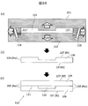
- Explanatory drawing which shows the preparation procedures of the resin-made microchip by injection molding. The figure which shows the example which grind
- Explanatory drawing which shows the example of the laser scattering in the bonding surface of a microchip.
- Explanatory drawing which shows the example of the laser scattering in the bonding surface of the curved microchip.
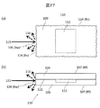
- Explanatory drawing which shows the example of the laser irradiation with respect to the microchip side surface cut and smoothed.
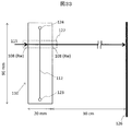
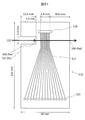
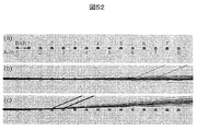
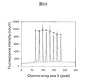
- the figure which shows the example of the microchip which has 15 channels.
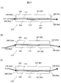
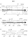
- FIG. 1A is a schematic cross-sectional view showing a typical example of a microchip 1 having an array of a plurality of channels 2 (hereinafter referred to as a channel array).
- 2 is a cross-sectional view including a transverse incident axis 3 (indicated by a dotted line in FIG. 1) of the microchip 1 and perpendicular to the major axes of a plurality of channels 2.
- FIG. The cross section of the microchip 1 is rectangular, and the long side of the rectangle is parallel to the transverse incident axis 3 and the channel arrangement.
- the major axes of the channels 2 are arranged in parallel to each other, on the same plane, and at a constant interval p.
- each channel 2 has No. 1 in order from the left side to the right side where the laser beam is introduced. Number 1, 2, 3, .... In FIG. 1 to 4 are shown. No. The distance between one channel and the left side surface of the microchip 1 is c.
- the cross section of each channel 2 has a tapered shape, here the same isosceles trapezoidal shape.
- the width of each channel 2 in the direction perpendicular to the transverse incident axis 3, that is, the height of the isosceles trapezoid is d.
- the microchip 1 is disposed in a medium having a refractive index n 0 .
- n 0 1.00.
- the member of the microchip 1 is a transparent solid member such as glass or resin, and the refractive index is n 1 .
- the member filled in each channel 2 is a liquid such as an aqueous solution or a gel material, and the refractive index is n 2 and n 2 ⁇ n 1 .
- a macrochip 1 having a channel 2 with an isosceles trapezoidal cross section can be manufactured by using a processing method having excellent mass productivity such as injection molding.
- the microchip 1 is composed of two upper and lower parts having a plane including the upper end surface of each channel 2 as a joint surface 4 (indicated by a one-dot chain line in FIG. 1), and these two parts are bonded together at the joint surface 4 to be integrated. Can be manufactured.
- the upper and lower parts are bonded together by a method such as thermocompression bonding. More preferably, the bonding surface 4 is optically transparent and does not include air or an adhesive layer.
- the joint surface 4 of the component below the joint surface 4 is provided with a plurality of grooves having a square cross section constituting the channel, and the joint surface 4 of the component above the joint surface 4 is a flat surface provided with no groove. is there. For this reason, even if the bonding positions of the upper and lower parts are shifted, the shape and position of each channel 2 are not affected. Injection molding requires a process of drawing a mold after pouring a member such as a resin into the mold, so that the cross-sectional shape of the groove that can be formed is a tapered shape whose width increases from the bottom of the groove toward the joint surface 4 It needs to be.
- the upper base of the isosceles trapezoid is the part of the joint surface 4 and the lower base is the bottom of the groove provided in the part below the joint surface 4, the width of the upper base> the lower base as shown in FIG.
- the process of extracting the mold in a processing method such as injection molding becomes easy, and the mass productivity can be increased.
- the base angle of the isosceles trapezoid the part exceeding 90 degrees is called draft. That is, when the draft is D degrees, the base angle of the isosceles trapezoid is 90 + D degrees.
- the draft D is 0 degree ⁇ D ⁇ 90 degrees, and the larger the D, the easier the process of extracting the mold, but it is desirable that the cross-sectional shape of each channel is uniform, and the smaller the D, the better. In consideration of machining accuracy, it is desirable that D> 2 degrees.
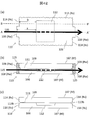
- FIGS. 1B and 1C schematically show optical paths when the laser beam 6 is irradiated on the microchip 1 of FIG. 1A under different conditions.
- the configuration of the microchip 1 and the irradiation condition of the laser beam 6 shown here are only representative examples for explaining the basic idea of the present invention, and other configurations and irradiation conditions based on the same idea are also described in this document. Needless to say, this is the subject of the invention.
- the cross-sectional shape of each channel 2 may not be an isosceles trapezoid, and the arrangement interval may not be constant.
- the laser beam 6 is irradiated from the left side surface of the microchip 1 in a state where the central axis 5 of the laser beam 6 coincides with or is parallel to the transverse incident axis 3. No. 1 before entering the microchip 1 and after entering the microchip 1.
- the width in the direction perpendicular to the arrangement plane of the laser beams 6 until reaching one channel, that is, the width in the direction perpendicular to the transverse incident axis 3 is b in FIG.
- the laser beam 6 is considered to be composed of a large number of infinitesimal beam elements.
- the laser beam 6 is collimated so that the beam elements are substantially parallel, and then the microchip 1 is irradiated. Among these beam elements, No.
- the central axis 5 and the upper and lower beam elements are drawn.
- the central axis 5 is drawn as a representative.
- the isosceles trapezoid which is the cross-sectional shape of each channel 2 can be regarded as a part of the cross section of an isosceles triangular prism, but the refractive index around the prism, that is, the refractive index n 1 of the member of the microchip 1, Since the refractive index of the prism, that is, the refractive index n 2 of the member filled in each channel 2 is smaller, the laser beam incident on the prism is on the opposite side of the base of the isosceles triangle, that is, on the apex angle side. Refract. This problem has been found for the first time in the present invention.
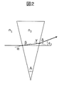
- FIG. 2 is a diagram showing the definition of the refraction angle of the laser beam incident on the isosceles triangular prism, and this phenomenon is schematically shown in an easy-to-understand manner.
- An isosceles triangular prism having a refractive index n 2 and having a cross section of an apex angle A is positioned in the member having the refractive index n 1 with the base side horizontal and the apex angle downward.
- the incident angle at the incident surface is ⁇
- the refraction angle is ⁇
- the incident angle at the exit surface when a virtually zero-width laser beam is horizontally incident on this prism, the incident angle at the incident surface is ⁇ , the refraction angle is ⁇ , and the incident angle at the exit surface.
- ⁇ , ⁇ , ⁇ , and ⁇ all take positive values between 0 ° and 90 °, but ⁇ 2 is ⁇ 90 ° ⁇ 2 ⁇ 90 °, and the sign of the laser beam is as shown in FIG.
- the case where the light is refracted toward the base side is positive, and the case where it is refracted toward the apex angle side is negative.
- ⁇ 2 is a refraction angle received when the laser beam 6 passes through the channel 2.
- the laser beam is refracted to the apex side when passing through the prism, and in FIG. 1B, the laser beam 6 is bonded in a direction away from the transverse incident axis 3 when passing through the channel 2.
- the light is refracted in the direction opposite to the surface 4.
- the central axis 5 of the laser beam 6 is not coincident with or parallel to the transverse incident axis 3, but is inclined by ⁇ 0 (> 0) with respect to the transverse incident axis 3.
- 1 is introduced from the left side, theta 1 with respect to the horizontal axis of incidence 3 (> 0) only inclined No. Irradiate one channel.
- the laser beam 6 is collimated so that the beam elements are substantially parallel, and then the microchip 1 is irradiated.
- the signs of the angles ⁇ 0 and ⁇ 1 are both positive when the laser beam 6 travels in the direction from the lateral incident axis 3 toward the bonding surface 4, that is, in the upper right direction in FIG. To do.
- the signs of the angles ⁇ 0 and ⁇ 1 are positive when the laser beam 6 is directed from the lower part of the microchip 1 provided with the groove toward the upper part without the groove.
- no. In the cross section of the channel No. 1, when the laser beam 6 goes in the direction in which the width of the tapered shape increases, that is, from the narrower side of the tapered shape to the wider side, No.
- the sign of angle ⁇ 1 is positive.
- the refraction angle ⁇ 2 ( ⁇ 0) of each channel increases the distance in the direction of the transverse incident axis 3 until the laser beam 6 deviates from the channel arrangement to the side opposite to the bonding surface 4, and a larger number of channels 2.
- the position where the laser beam 6 is introduced into the left side surface of the microchip 1 is not on the lateral incident axis 3, but is shifted by a (> 0) from the lateral incident axis 3 to the side opposite to the bonding surface 4.
- No. 1 channel can be irradiated well.
- it is important that the magnitude of ⁇ 1 is not too large or too small and is within an appropriate range.
- ⁇ 1 90 degrees, that is, in the case of irradiating the laser beam 6 perpendicularly to the transverse incident axis 3 from bottom to top in FIG.
- the laser beam 6 that has passed through the channel 2 of No. 1 Since it is not possible to irradiate the channels after the second, it cannot be a lateral incidence method, and a plurality of channels cannot be efficiently irradiated simultaneously.
- no. No. 1 channel is irradiated, and the laser beam 6 that has passed through is at least No. 1. It is necessary to illuminate two channels. For this purpose, no.
- the beam element incident on the lower end of the channel No. 1 is No. 1.
- the angle ⁇ 3 formed by the beam element toward 3 to No. 4 is the angle ⁇ 4 formed by the beam element toward the transverse incident axis 3, and (L-1) to No.
- L indicates the total number of channels that are simultaneously irradiated.
- ⁇ 2 , ⁇ 3 , ⁇ 4 ,..., ⁇ L The sign of ⁇ 2 , ⁇ 3 , ⁇ 4 ,..., ⁇ L is the same as that for ⁇ 1 and ⁇ 2 .
- ⁇ 1 , ⁇ 2 , ⁇ 3 , ⁇ 4 ,..., ⁇ L start from positive and eventually turn negative.
- ⁇ 1 to ⁇ 3 are positive, but turn to negative after ⁇ 4 .
- Up to channel 3 is deflected upward, and thereafter, it is deflected downward.
- int (X) is a function for deriving the integer part of X.
- the laser beam 6 is irradiated from the side surface of the microchip 1 as shown in FIG.
- ⁇ 1 according to equation (18) is much larger than ⁇ 1 according to equation (8), so there is no ⁇ 1 compatible with equation (9) or equation (15).
- the present invention inevitably has a configuration in which the laser beam 6 is irradiated from the side surface of the microchip 1 and cannot be applied to the case of irradiation from the lower surface or the upper surface of the microchip 1. This is fundamentally different from the conventional method (1) beam expansion method and (2) beam scan method.
- the configuration shown in FIG. 1C can simultaneously irradiate a larger number of channels 2 by the lateral incidence method as compared with the configuration shown in FIG.
- the number of channels 2 that can be irradiated simultaneously with individual beam elements in the configuration of FIG. 1C is about 2 to 3 times that in the configuration of FIG. 1B.
- the width b of the laser beam 6 is made larger than the width d of each channel 2, first, as shown in FIG. The beam element irradiating the channel 2 of No.
- the width b of the laser beam 6 suitable for realizing an efficient lateral incidence method depends on the total number L of channels 2 to be simultaneously irradiated.
- L does not necessarily match the total number of channels 2 included in the microchip 1. If there are beam elements that irradiate each of the L channels 2 first, all L channels 2 can be irradiated simultaneously.
- the width of the laser beam 6 incident from the left side surface of the microchip 1 in the direction of the transverse incident axis 3 is 1 channel 2 and no.
- the distance of channel 2 of L should be larger than p ⁇ (L ⁇ 1), and the condition is b> p (L ⁇ 1) tan ⁇ 1 (19) It is.
- Equation (19) a condition for simultaneously irradiating all L channels 2 more efficiently while reducing the size of b from Equation (19).
- the number of channels 2 that can be irradiated simultaneously by the individual beam elements in the configuration of FIG. 1C is twice that of the configuration of FIG. 1B as a typical example
- the number of channels 2 can be calculated using equation (14). Can be expressed as 2 ⁇ M ⁇ 1.
- M is assumed.
- the effect of enlarging the width d in the vertical direction has been described.
- the width in the direction parallel to the arrangement plane of the laser beams 6, that is, the width in the major axis direction of each channel 2 is not subjected to the same enlargement. Many. There are two reasons for this.
- each channel 2 is analyzed by laser beam irradiation and fluorescence detection, the laser beam width in the major axis direction of each channel 2 becomes larger than the width of each channel 2. Electrophoretic resolution is reduced. The other is that if the laser beam 6 is expanded not only in the direction perpendicular to the arrangement plane but also in the parallel direction, the laser beam intensity density is reduced by that amount, so that the irradiation efficiency and fluorescence detection sensitivity of each channel 2 are reduced. It is because it ends up.
- the laser beam 6 is expanded only in the direction perpendicular to the arrangement plane, that is, the microchip 1 and each channel are shaped so that the cross section of the laser beam 6 is elliptical or linear. 2 is good.
- the direction of measuring scattered light or fluorescence from each channel 2 by irradiation with the laser beam 6 may be from above or below the microchip 1 in FIG. That is, even if FIG. 1 is turned upside down, the contents of the above invention are not affected.
- the center axis of the light detection system is perpendicular to at least one of the arrangement plane of the channels 2, the upper surface or the lower surface of the microchip 1. It is good for improving sensitivity and reducing variations.
- ⁇ 0 , ⁇ 1 , ⁇ 2 ,..., ⁇ L are defined as angles that form the transverse incident axis 3 of the laser beam 6 or the array plane, but these angles are perpendicular to the central axis of the light detection system. It may be defined as an angle with respect to a simple plane.
- FIG. 3 is a process diagram showing a cross-sectional schematic view of a process for manufacturing the microchip 1 shown in FIG. 1 by injection molding.
- a member in which a transparent resin is heated and melted as shown in (b) is injected and injected into the mold 7 shown in (a), and cooled and solidified.
- a component 8 having a plurality of grooves to be channels of the microchip 1, that is, a component 8 below the bonding surface 4 of the microchip 1 is obtained as shown in FIG.
- the member of the component 8 is a transparent solid member having a refractive index n 1 .
- the component 8 is obtained by forming a plurality of grooves having a trapezoidal cross-sectional shape on the surface of a plate-like transparent solid member. The grooves are arranged in parallel to each other in at least some areas.
- a plate-like transparent solid member having a refractive index n 1 is separately produced as a component 9 that does not have a channel of the microchip 1, that is, a component 9 above the bonding surface 4 of the microchip 1. and, bonding by thermal welding or the like at the joining surface 4 and part 8, (e), the obtaining microchip 1 of refractive index n 1. That is, by this process, a plurality of channels 2 are formed inside the microchip 1 by a plurality of grooves formed on the surface of the component 8. In this state, the interior of each channel 2 is filled with air.
- a plurality of channels 2 are filled with a medium having a refractive index n 2 used for analysis, thereby producing channels 2.
- the microchip 1 is distributed to users in the state (e) or (f), for example. Since the component 9 has a flat surface, it may have a flexible thin sheet shape, for example, a thickness of about 100 ⁇ m. Thus, making the component 9 into a thin sheet shape contributes to reducing the manufacturing cost of the microchip 1. In this embodiment, the direction in which the laser beam 6 is refracted is away from the bonding surface 4, so that there is no particular problem caused by the thickness of the component 9 being reduced.
- the same effect can be obtained even if the cross-sectional shape of the channel 2 is other than the trapezoid.
- At least the cross-sectional shape of the channel 2 that can be manufactured by a processing method such as injection molding or nanoimprinting is an object.
- the same effect can be obtained even if the trapezoid, triangle, or each side of the trapezoid or triangle is not a straight line but is arcuate, or the corners of the trapezoid or triangle are rounded.
- D the case of such a general cross-sectional shape, it can be considered that the above relational expression is established by obtaining D as follows.
- the minimum value of the width parallel to the transverse incident axis of the cross-sectional shape of each channel is W min
- the maximum value is W max
- the maximum value of the width perpendicular to the transverse incident axis is d.
- W min is obtained at a position farthest from the joint surface
- W max is obtained at a position closest to the joint surface.
- D 90 ⁇ tan ⁇ 1 ⁇ 2d / (W max ⁇ W min ) ⁇ .
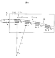
- FIG. 4 is a schematic cross-sectional view of a microchip including a plurality of channels showing another solution.
- the center positions of the channels 2 irradiated with the laser beam are arranged on the same straight line, that is, on the horizontal incident axis 28 without being arranged on the horizontal incident axis 3.
- the channel arrangement is not on the plane including the lateral incident axis 3 but on the curved surface including the lateral incident curve 28. That is, the long axes of the plurality of channels 2 are arranged on a cylindrical surface having a radius of curvature R.
- the plurality of channels have a tapered shape (here, an isosceles trapezoidal shape) in a cross section perpendicular to the long axis.
- the laser beam 6 transmitted through the channel 2 of No. 1 is No. 1. No. 1 due to the refraction action by channel 2. It advances at an angle of ⁇ 2 with respect to the laser beam 6 before entering the channel 2 of 1. Therefore, the central axis 5 is No. No. 2 is parallel to the upper and lower bases of the isosceles trapezoid that is the cross section of the channel 2, and No.
- the joint surface 4 is also curved in the same manner as the lateral incidence curve 28.
- the transverse incidence curve 28 is curved in the same direction as the direction in which the laser beam 6 is refracted by each channel 2. That is, when the upper base> the lower base in the isosceles trapezoidal shape of the cross section of the channel 2, the lateral incident curve 28 is curved in the direction from the upper base to the lower base.
- the transverse incidence curve 28 is curved in the opposite direction from the center of the channel 2 toward the bonding surface 4 of the microchip 1.
- the radius of curvature R indicating the degree of curvature is preferably constant regardless of the position when the arrangement interval p of the channels 2 is constant.
- the arrangement position of the channels 2 is curved with a constant curvature radius R over a region where the plurality of channels 2 to be measured are arranged.
- the upper and lower surfaces of the microchip 1 are No. 1 is parallel to the direction of the laser beam 6 before entering the channel 2, and the left side surface and the right side surface of the microchip 1 are No. 1.
- the direction in which scattered light or fluorescence from each channel 2 due to the irradiation of the laser beam 6 is measured may be from above or below the microchip 1 in FIG. That is, even if FIG. 4 is turned upside down, the contents of the above invention are not affected.
- Making the central axis of the light detection system perpendicular to the plane including both of the long axes of the L channels 2 can improve the light detection sensitivity of each channel 2 and reduce variations.
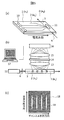
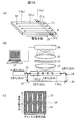
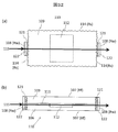
- FIG. 5 is a schematic explanatory diagram showing an example of a multi-channel analyzer according to the present invention.
- This embodiment shows a system for performing electrophoretic analysis of DNA contained in a biological sample, (a) is a bird's-eye view of the microchip 1, and (b) is a transverse incident axis 3 of a laser beam 6 with respect to the microchip 1 constituting the system. , A cross section of the fluorescence detection optical systems 13 to 16, and the data analysis device 17, and (c) shows a two-dimensional fluorescence image 18 obtained by the two-dimensional sensor 16.
- Laser scattered light and fluorescence wavelength dispersion images 19 from each channel 2 due to excitation of the laser beam 6 are measured independently of each other. With the above configuration, it is possible to identify a small amount of fluorescence by increasing the number of types of fluorescence that can be simultaneously detected in each channel 2 or by separating and detecting different fluorescence with high accuracy. In this example, different samples were labeled with different phosphors and analyzed simultaneously in the same channel to improve throughput.
- the medium 0 of refractive index n 0, are arranged microchip 1 is composed of members of the refractive index n 1, members of the refractive index n 2 in the microchip 1
- a plurality of channels 2 filled with are arranged.
- Each channel 2 is provided with an inlet port 10 and an outlet port 11 common to each channel 2.
- Each of the channels 2 in the vicinity of the inlet port 10 is provided with a cross injection part or a double T injection part for introducing a sample, which is omitted in FIG.
- a region of interest is amplified in advance and a fluorescent substance is labeled.
- each channel 2 After the sample is introduced, by applying a voltage to both ends of each channel 2 with the inlet port 10 as the negative electrode and the outlet port 11 as the positive electrode, the fluorescently labeled DNA contained in the sample is electrophoretically separated from the inlet port 10 toward the outlet port 11.
- the plurality of channels 2 are arranged such that the long axes of the channels are substantially parallel to each other in at least a part of the region.
- the laser beam generated from the laser light source is incident from the side surface of the microchip substantially perpendicularly to the long axes of a plurality of channels arranged substantially parallel to each other.
- the laser beam 6 emitted from the laser light source 12 is stopped by an irradiation optical system including a lens, introduced from the side surface of the microchip 1, and each channel 2 is irradiated.
- 5A and 5B for simplicity, the center axis 5 of the laser beam 6 introduced into the microchip 1 and the lateral incident axis 3 are expressed as being coincident or parallel, but it is accurate. As described above and as will be described later with reference to FIG. 21, these have a significant angle.
- the fluorescently labeled DNA that is electrophoresed in each channel 2 is excited by the laser beam 6 when it crosses the position where the laser beam 6 is irradiated, and emits fluorescence.
- the fluorescence emitted from each channel 2 is detected by a fluorescence detection optical system. That is, the light is collimated by the common condenser lens 13, passes through the filter and the diffraction grating 14, and is imaged on the sensor surface of the two-dimensional sensor 16 by the imaging lens 15.
- the filter is provided in order to block the wavelength of the laser beam 6 which becomes background light in fluorescence detection
- the diffraction grating is provided in order to detect the multicolor by wavelength dispersion of the fluorescence. Since the cross section of the channel 2 has the same shape with respect to the long axis direction of the channel 2, the same effect can be obtained even if the incident position of the laser beam 6 on the microchip 1 is slightly shifted in the long axis direction of the channel 2. Is obtained and the fluorescence detection sensitivity is not affected.
- FIG. 5C is a schematic diagram showing a two-dimensional fluorescent image 18 obtained by the two-dimensional sensor 16.
- the direction of chromatic dispersion is the long axis direction of each channel 2 (the direction perpendicular to the cross-sectional view of FIG. 5B), that is, the direction perpendicular to the arrangement direction of the plurality of channels 2.
- the chromatic dispersion images are measured independently without overlapping each other.
- a laser light scattering and fluorescence wavelength dispersion image 19 that cannot be completely removed by the filter is obtained.
- the fluorescence signal thus measured is analyzed by the data analyzer 17 and the sample introduced into each channel 2 is analyzed.
- FIG. 21 is a schematic cross-sectional view showing in detail the laser beam 6, the microchip 1 and the plurality of channels 2 shown in FIG. 5, and shows a mechanism for controlling the angle formed between the laser beam and the transverse incident axis. It is explanatory drawing.
- the microchip 1 and the analyzer are simply installed on the stage 27 of the analyzer. It is desirable that the parameters defined above, such as the angle ⁇ 1 of the laser beam 6 irradiated to one channel 2 with respect to the transverse incident axis 3, are designed to have desired values. However, it is assumed that ⁇ 1 and the like deviate from the designed values due to variations in processing accuracy of the microchip 1, deformation due to deterioration, or deformation due to environmental factors of the analyzer.
- FIG. 21A shows an example of a calibration mechanism.
- the irradiation angle of the laser beam 6 with respect to the microchip 1 becomes a desired angle ⁇ 1.
- FIG. 21B the position and angle of the stage 27 are controlled by the adjustment mechanism 26 so that a desired angle ⁇ 1 can be obtained.
- the adjustment mechanism of FIG. 21A and the adjustment mechanism of FIG. 21B may be used in combination.
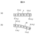
- the relative angle between the laser beam 6 and the microchip 1 is adjusted by the adjusting mechanism 26 in FIG. 21 (a) or FIG. 21 (b). It is effective to adjust the signal intensity so that the signal intensity approaches the design value. It is convenient to use the Raman scattering intensity of water obtained from each channel 2 as the signal intensity. It is also effective to incorporate a calibration marker in the microchip 1 separately from the channel 2 used for sample analysis. For example, as shown in FIG. 24A, calibration channels 31 are provided on both sides of the array of channels 2 used for analysis. The channel 31 is filled with a medium having a refractive index n 2 and a relatively strong Raman scattering, similar to the channel 2.
- the adjusting mechanism 26 shown in FIG. 21A or 21B is controlled to obtain an appropriate relative angle. Furthermore, since the light emission from the channel 31 can be measured simultaneously and independently with the light emission from the channel 2 by the fluorescence detection optical system shown in FIG. 5B, the adjustment mechanism 26 is controlled in real time while analyzing. You can also. This is effective as a countermeasure when the microchip is deformed due to a temperature rise or the like during the analysis.
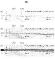
- a ray tracing simulation of the laser beam 6 incident on the plurality of channels 2 provided on the microchip 1 is performed, and the laser beam before being incident horizontally
- the ratio of the intensity of the laser beam 6 passing through the inside of each channel 2 to the total intensity of 6, that is, the laser beam irradiation efficiency for each channel 2 is obtained, and how many channels can be incident laterally with what efficiency Evaluated. It has been proved that the laser beam irradiation efficiency for each channel 2 obtained from such ray tracing simulation agrees well with the fluorescence intensity ratio for each channel 2 obtained in the experiment, as shown in known literature. , It is an extremely reliable evaluation method.
- lighting design analysis software LightTool TM (Synopsys' Optical Solutions Group) was used as a three-dimensional ray tracing simulator.
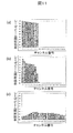
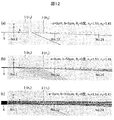
- FIGS. 6, 8, 10, 12, 14, and 16 show the results of ray tracing simulation.
- the wavelength of the laser beam 6 is 505 nm.
- no. 1 to No. A total of 24 24 channels 2 are arranged on the same plane. That is, L 24.
- Reference numeral 1 denotes an end on the side where the laser beam 6 is introduced, and indicates the number of the channel 2 to which the laser beam 6 is first irradiated. Thereafter, in order of each channel 2 along the traveling direction of the laser beam 6, 2, no. 3, ... No. Number 24.
- Each figure is represented by a yz plane consisting of a y-axis and a z-axis. The center of the channel 1 of 1 and the z axis are aligned with the transverse incident axis 3.
- the member of the microchip 1 was ZEONOR TM (Zeonor, Nippon Zeon).
- ZEONOR is a cycloolefin polymer (COP) resin, and is often used as a microchip member due to its high transparency and low hygroscopicity.
- each channel 2 was the same isosceles trapezoid.
- the cross-sectional shape of the channel 2 is an isosceles trapezoid is to improve the mass productivity of the microchip 1 as described above.
- the surface including the upper base of each isosceles trapezoid is the joint surface 4.
- the laser beam 6 is composed of 300 infinitely small beam elements, and the positions of these beam elements are uniform and random within the respective diameters (a), (b), and (c) of each figure. Arranged. Further, the total intensity of the laser beam 6 before entering the microchip 1 is set to 1.00 (100%), and each beam element is equally given an intensity of 1/300 (0.33%). .
- Snell's law and the refraction index at each position where the refractive index changes such as the entrance surface to the microchip 1, the entrance surface to each channel 2, and the exit surface from each channel 2, for each beam element. Fresnel's law was applied to track the direction and intensity of refracted light. However, when the beam element was totally reflected at the position where the refractive index changed, the traveling direction and intensity of the reflected light were tracked. Each figure shows the optical path of 300 beam elements thus calculated.
- the buffer solution was filled in each channel 2.
- the laser beam irradiation efficiency is No. Channel 2 of 1 is the same as that of FIG. No. 1 monotonically decreases in channel 2 and later. It became zero in channel 2 after 7.
- the condition of b 300 ⁇ m in FIG. 6C is a typical example in the case where the laser beam 6 is laterally incident with a diameter larger than that of the channel 2. No. Since there are many beam elements that do not contribute to irradiation in all the channels 2 after 1 and the effective laser beam intensity is reduced by that amount, the laser beam irradiation efficiency in FIG. In case of (b), it is reduced to about 1/5. It became zero in channel 2 after 7. In FIG.
- Expression (16) is satisfied.
- the condition that satisfies the equation (17) is ⁇ 1 > 0.52 degrees, and the equation (17) is also satisfied.
- the condition that satisfies the equation (9) is ⁇ 1 ⁇ 10.00 degrees, and the equation (9) is also satisfied.
- the condition that satisfies Expression (15) is ⁇ 1 ⁇ 3.46 degrees, and Expression (15) is not satisfied.
- the other conditions and display methods of FIGS. 8 and 9 are the same as those of FIGS.
- FIG. 8A shows the irradiation of more channels 2 as compared with FIG. 6A as a result of the increased distance in the direction of the transverse incident axis 3 until the laser beam 6 deviates from the channel 2 arrangement. It shows that it contributes to.
- Irradiation of 11 channels 2 of 1 to 11 is possible, and the number of channels that can be irradiated at the same time is greatly increased as compared with the four channels of FIG.
- the average value of the laser beam irradiation efficiency decreases and the variation increases.
- 8 (b) and 9 (b) show that the number of channels that can be irradiated simultaneously has increased from 6 to 11 compared to FIGS. 6 (b) and 7 (b) due to the same effect. It shows that.
- ⁇ 1 > 0.00 degrees in equation (16) ⁇ 1 > 0.52 degrees in equation (17), ⁇ 1 ⁇ 10.00 degrees in equation (9), ⁇ 1 ⁇ 3.46 degrees is all satisfied.
- more efficient laser beam lateral incidence can be realized as compared with the cases of FIGS.
- FIGS. 10 (a) and 11 (a) compared to FIGS. 8 (a) and 9 (a), the condition (15) is satisfied, so that the condition for the more lateral incidence is obtained, and simultaneous irradiation is performed.
- the number of possible channels is reduced from 11 to 9, the average value of the laser beam irradiation efficiency is greatly improved and the variation is greatly reduced.
- FIG. 10B and FIG. 11B the number of channels that can obtain a laser beam irradiation efficiency of 70% or more as compared with FIG. 8B and FIG. It has increased from seven to seven. This is an important performance for performing highly sensitive analysis in a large number of channels.
- a microchip provided with a plurality of channels each having an isosceles trapezoidal cross section perpendicular to the major axis is used, and the laser beam is tilted from the side surface of the microchip by ⁇ 1 > 0 with respect to the transverse incident axis.
- the channel whose cross-sectional shape perpendicular to the long axis is an isosceles trapezoid has been described as an example.
- the cross-section is triangular, or each side is not a straight line but an arc.
- the same effect can be obtained.
- the same effect can be obtained for a microchip provided with a plurality of channels each having a tapered shape with a cross section perpendicular to the major axis widening toward the end.
- the laser beam 6 is introduced from the lower surface of the microchip 1 .
- Equation (18) No.
- the angle of the laser beam 6 irradiated to one channel 2 with respect to the transverse incident axis 3 is ⁇ 1 > 50 degrees with respect to an arbitrary ⁇ 0 . Therefore, neither ⁇ 1 ⁇ 10.00 degrees in Expression (9) nor ⁇ 1 ⁇ 3.46 degrees in Expression (15) can be satisfied, and an efficient lateral incidence method cannot be realized. Therefore, in this embodiment, the laser beam 6 is not necessarily introduced from the upper surface or the lower surface of the microchip 1, but is introduced from the side surface of the microchip 1.
- Example 2 In the present embodiment, the difference from the first embodiment will be mainly described, and if there is no particular description, it may be considered that the same description as in the first embodiment holds.
- the member filled in each channel 2 was changed from a buffer solution to a 3500/3500 ⁇ L POP-7 TM polymer solution (Life Technologies).
- POP-7 is an aqueous solution containing 8M urea and a polymer as an electrophoretic separation medium, and is used for DNA sequencing.
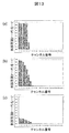
- Expression (16) is satisfied.
- the condition that satisfies the equation (17) is ⁇ 1 > 0.31 degrees, and the equation (17) is also satisfied.
- the condition that satisfies the equation (9) is ⁇ 1 ⁇ 9.74 degrees, and the equation (9) is also satisfied.
- the condition that satisfies Expression (15) is ⁇ 1 ⁇ 2.68 degrees, and Expression (15) is not satisfied.
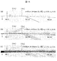
- FIGS. 14A and 14B the central axis 5 of the laser beam 6 is No.
- FIG. 14C the vicinity of the upper end of the laser beam 6 is No. 1 channel 2 was irradiated.
- Other conditions, display methods, and the like in FIGS. 14 and 15 are the same as those in FIGS. 12 and 13.
- FIG. 14A shows the irradiation of more channels 2 as compared with FIG. 12A as a result of increasing the distance in the direction of the transverse incident axis 3 until the laser beam 6 deviates from the channel 2 arrangement. It shows that it contributes to.
- FIG. It is possible to irradiate 14 channels 2 of 1 to 14, and the number of channels that can be irradiated at the same time is greatly increased as compared with 6 channels in FIG.
- the average value of the laser beam irradiation efficiency decreases and the variation increases.
- 14 (b) and 15 (b) show that the number of channels that can be irradiated simultaneously has increased from 8 to 14 compared to FIGS. 12 (b) and 13 (b) due to the same effect. It shows that.
- the effect is particularly high in that the number of channels capable of obtaining a laser beam irradiation efficiency of 30% or more is increased from 6 to 13.
- the effect is particularly high in that the number of channels capable of obtaining a laser beam irradiation efficiency of 30% or more is increased from 0 to 16.
- ⁇ 1 ⁇ 9.74 degrees in equation (9) All ⁇ 1 ⁇ 2.68 degrees are satisfied. This makes it possible to realize a more efficient laser beam lateral incidence as compared with the cases of FIGS.
- the position where the central axis 5 of the laser beam 6 is incident on the side surface of the microchip 1 is lower than the lateral incident axis 3, that is, away from the bonding surface.
- the other conditions, display methods, and the like in FIGS. 10 and 11 are the same as those in FIGS.
- FIG. 16A and FIG. 17A compared with FIG. 14A and FIG. 15A, the condition (15) is satisfied, so that the conditions suitable for further lateral incidence are obtained.
- the number of possible channels is only 11, the average value of the laser beam irradiation efficiency is greatly improved and the variation is greatly reduced.
- FIG. 16B and FIG. 17B the number of channels that can obtain a laser beam irradiation efficiency of 70% or more as compared with FIG. 14B and FIG. The number has increased from nine to nine. This is an important performance for performing highly sensitive analysis in a large number of channels.
- 16C and 17C show an average value of the laser beam irradiation efficiency for 24 channels 2 from 32% to 18% as compared with FIGS. 14C and 15C.
- a microchip provided with a plurality of channels each having an isosceles trapezoidal cross section perpendicular to the major axis is used, and the laser beam is tilted from the side surface of the microchip by ⁇ 1 > 0 with respect to the transverse incident axis.
- the channel whose cross-sectional shape perpendicular to the long axis is an isosceles trapezoid has been described as an example.
- the cross-section is triangular, or each side is not a straight line but an arc.
- the same effect can be obtained.
- the same effect can be obtained for a microchip provided with a plurality of channels each having a tapered shape with a cross section perpendicular to the major axis widening toward the end.
- the laser beam 6 is introduced from the lower surface of the microchip 1 .
- Equation (18) No.
- the angle of the laser beam 6 irradiated to one channel 2 with respect to the transverse incident axis 3 is ⁇ 1 > 50 degrees with respect to an arbitrary ⁇ 0 . Therefore, neither ⁇ 1 ⁇ 9.74 degrees in Expression (9) nor ⁇ 1 ⁇ 2.68 degrees in Expression (15) can be satisfied, and an efficient lateral incidence method cannot be realized. Therefore, in this embodiment, the laser beam 6 is not necessarily introduced from the upper surface or the lower surface of the microchip 1, but is introduced from the side surface of the microchip 1.
- Example 3 shows a system for performing electrophoretic analysis of DNA contained in a biological sample, where (a) is a bird's-eye view of the microchip 1 and (b) is lateral incidence of the laser beam 6 and the laser beam 20 of the microchip 1.
- the medium 0 of refractive index n 0, are arranged microchip 1 is composed of members of the refractive index n 1, members of the refractive index n 2 in the microchip 1
- a plurality of channels 2 filled with are arranged.
- Each channel 2 is provided with an inlet port 10 and an outlet port 11.
- a laser beam 6 having a wavelength of 505 nm and a laser beam 20 having a wavelength of 635 nm are introduced from the side surface of the microchip 1 and the array of channels 2 is irradiated by transverse incidence. ing.
- the laser beam 6 and the laser beam 20 irradiate a position shifted in the major axis direction of each channel 2, that is, the lateral incident axis 3 and the lateral incident axis 21, respectively. Since the conditions such as the cross-sectional shape of each channel, the arrangement interval, the refractive index, and the like are the same for any transverse incident axis, an equivalent transverse incidence method can be realized. In general, since the refractive index of each member differs depending on the wavelength, it may affect the performance of the lateral incidence method. However, since the wavelength dependency of the refractive index of each member used in this embodiment is small, the influence Is small.
- the laser beam 6 and the laser beam 20 are each divided into two and then irradiated from both side surfaces of the microchip 1.
- the use of a plurality of types of laser beams and the introduction of each laser beam from both sides of the microchip may be performed simultaneously as described above, or of course only one of them.
- Other structures of the microchip 1 and irradiation conditions of the laser beams 6 and 20, for example, the laser beam width b perpendicular to the array plane and the transverse incident axis, and the angle ⁇ 1 between the central axis of the laser beam and the transverse incident axis are implemented. Equivalent to any of the conditions shown in Example 1 or Example 2.
- the laser beams 6 and 20 emitted from the laser light sources 12 and 22 are irradiated from both side surfaces of the microchip 1 after being divided into two by using the half mirror 23 and the mirror 24.
- the central axis of the laser beam 6 and the laser beam 20 introduced into the microchip 1 and the lateral incident axis 3 and the lateral incident axis 21 are respectively coincident or parallel to each other.
- they have a significant angle.
- the fluorescently labeled DNA that is electrophoresed in each channel 2 is excited when it crosses the position where the laser beam 6 and the laser beam 20 are irradiated, and emits fluorescence.
- the fluorescence emitted from each channel 2 is detected by the fluorescence detection optical systems 13-16. That is, the light is collimated by the common condenser lens 13, passes through the filter and the diffraction grating 14, and is imaged on the sensor surface of the two-dimensional sensor 16 by the imaging lens 15.
- the filter is provided to block the wavelengths of the laser beam 6 and the laser beam 20 which are background light at the time of fluorescence detection, and the diffraction grating is provided for multi-color detection by wavelength dispersion of fluorescence.
- FIG. 18C is a schematic diagram showing a two-dimensional fluorescent image 18 obtained by the two-dimensional sensor 16.
- the direction of chromatic dispersion is the long axis direction of each channel 2 (the direction perpendicular to the cross-sectional view of FIG. 18B), that is, the direction perpendicular to the arrangement direction of the plurality of channels 2.
- the laser light scattering and fluorescence wavelength dispersion image 19 from 2 and the laser light scattering and fluorescence wavelength dispersion image 25 from each channel 2 by excitation of the laser beam 20 are measured independently. With the above configuration, it is possible to identify a small amount of fluorescence by increasing the number of types of fluorescence that can be simultaneously detected in each channel 2 or by separating and detecting different fluorescence with high accuracy. In this example, different samples were labeled with different phosphors and analyzed simultaneously in the same channel to improve throughput.
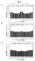
- FIG. 25 shows the effect when the laser beam 6 is divided into two parts and irradiated from both side surfaces of the microchip 1. As shown below, laser beam irradiation from both sides increases the number of channels 2 that can be irradiated simultaneously, and reduces variations in laser beam irradiation efficiency between channels 2 to obtain uniform fluorescence detection sensitivity. It is an effective means.
- FIG. 19 shows the laser beam irradiation efficiency in each channel 2 when the number is reduced from 16 to 16 and the laser beam 6 is divided into two according to FIG. 18 and irradiated from both side surfaces of the microchip 1.
- one of the two divided laser beams 6 is No. 1 from the side surface of the microchip 1 as in FIG. 1 channel 2 is irradiated, and the other is No. 1 from the opposite side of microchip 1.
- 16 channels 2 are irradiated. No. 1 and no.
- the two divided laser beams 6 that respectively irradiate the 16 channels 2 are in the center of the channel arrangement, that is, No. 1. 8 and no. 9 is made to be symmetric with respect to a plane passing through the midpoint of the channel 2 and perpendicular to the transverse incident axis 3.
- the total number of channels 2 that can be irradiated simultaneously is 10
- the laser beam irradiation efficiency of these 10 channels 2 is 65% on average
- the standard deviation is 26%
- the CV value is 40%.
- the total number of channels 2 that can be irradiated simultaneously increases to 16, and the laser beam irradiation efficiency of these 16 channels 2 is an average of 41%, which is slightly small. Uniform irradiation is possible between channels with a deviation of 5% and CV value of 12%.
- FIG. 19 shows the laser beam irradiation efficiency in each channel 2 when the number is reduced from 20 to 20 and the laser beam 6 is divided into two according to FIG. 18 and irradiated from both side surfaces of the microchip 1. Similarly, no. 1 and no. The two divided laser beams 6 irradiating each of the 20 channels 2 are in the center of the channel arrangement, that is, No. 10 and no. 11 is symmetric with respect to a plane passing through the midpoint of the channel 2 and perpendicular to the transverse incident axis 3.
- the total number of channels 2 that can be irradiated simultaneously is 12
- the laser beam irradiation efficiency of these 12 channels 2 is 70% on average, 26% standard deviation, and 37% CV value.
- the total number of channels 2 that can be irradiated simultaneously is increased to 20, and the laser beam irradiation efficiency of these 20 channels 2 is an average 42%, which is a little small. Uniform irradiation is possible between channels with a deviation of 2% and CV value of 6%.
- the microchip 1 in which the channel arrangement is curved can be manufactured by several methods.
- One manufacturing means is to design a mold in advance so that a desired radius of curvature can be obtained at the stage of manufacturing the parts of the microchip 1 below and above the joint surface 4 in FIG. 4 by injection molding. It is.
- the curved surface is excellent at injection molding, and it is also easy to join two parts having the same radius of curvature by thermocompression bonding or the like.
- FIG. 22 is a schematic cross-sectional view of the microchip 1 in which a plurality of channels 2 are curvedly arranged on an arc having a desired radius of curvature, that is, on a lateral incidence curve 28.
- the microchip shown in FIG. 22A is an example in which the upper surface and the lower surface of the microchip 1 are parallel to the laser beam 6 introduced into the microchip 1 as in FIG.
- Such a microchip 1 can be easily installed in the analyzer and the laser beam 6 can be easily adjusted.
- the microchip shown in FIG. 22B is an example in which the upper surface and the lower surface of the microchip 1 are curved surfaces having the same radius of curvature as the lateral incidence curve 28.
- the surface of the stage 29 that contacts the microchip 1 that fixes the microchip 1 to the analyzer also has the same radius of curvature as the lateral incidence curve 28. It should be a curved surface.
- it is effective to press the microchip 1 against the stage 29 by applying a pressing force 30 to the microchip 1 so that a desired radius of curvature is maintained.
- a pressing force 30 As means for generating the pressing force, a screw tightening force, a motor pressing force, or the like can be used.
- Another manufacturing means is that the upper and lower parts of the microchip 1 are not bent at the stage of injection molding, but the bending pressure is applied to the microchip 1 at the stage of joining or after joining them.
- the microchip 1 To obtain a desired radius of curvature as shown in FIG. Moreover, you may perform such a deformation
- the microchip 1 In order to generate a radius of curvature at the stage after injection molding, the microchip 1 should be designed to be easily bent. For this purpose, it is effective to make the thickness of the components of the microchip 1 below and above the bonding surface 4 as thin as possible.
- the part below the bonding surface 4 of the macrochip 1 has a plurality of grooves for forming the channel 2 and is curved, so that it is easy to reduce the thickness of this part. is not.
- the upper part can be a resin sheet having a thickness of about 100 ⁇ m.
- the draft angle D of each channel 2 may slightly increase in order to absorb the distortion. In that case, the curvature radius of the curve must be reduced accordingly. Increased amount of draft is about 2 even ⁇ at the maximum, and because it is D»ipushiron 2, it is possible to so balanced. In any case, the radius of curvature should be designed according to the draft at the time of measurement.
- the parameters defined above for realizing an efficient transverse incidence method such as the curvature radius R of the transverse incidence curve 28 on which the center of each channel 2 rides are desired. It is desirable that the microchip 1 and the analysis device are designed so that the values can be obtained or the plurality of channels 2 can be efficiently irradiated with the laser beam. However, it is assumed that R or the like deviates from the designed value due to variations in processing accuracy of the microchip 1, deformation due to deterioration, or deformation due to environmental factors of the analyzer.
- the analyzer is provided with a calibration mechanism that can adjust R or the like to a design value by adjusting, or can more efficiently irradiate a plurality of channels 2 with a laser beam.
- the magnitude of the pressing force 30 in FIG. 23 (a) or FIG. 23 (b) is adjusted while monitoring the signal intensity from each channel 2 on the analyzer.
- it is effective to control the degree of curvature of the microchip 1 so that the signal intensity approaches the design value or to efficiently irradiate the plurality of channels 2 with the laser beam.
- the contact surface of the stage 29 that fixes the microchip 1 does not necessarily have a radius of curvature equivalent to that of the lateral incidence curve 28 as shown in FIG. 23 (a) or FIG. 23 (b). Rather, the curvature radius of the lateral incidence curve 28 can be controlled over a wide range including the curvature radius considered to be optimal by providing the contact surface with a curvature radius substantially smaller than the curvature radius considered to be optimal in design. Is effective. In such an adjustment method, the microchip 1 is deformed due to heat generation or the like during the analysis, or the refractive index of each member changes, so that R or the like changes or the optimum value of R or the like is changed. It is also effective to carry out during the analysis if it has changed.
- the Raman scattering intensity of water is convenient to use as the signal intensity. It is also effective to incorporate a calibration marker in advance inside the microchip 1 separately from the channel used for sample analysis.
- calibration channels 31 are provided on both sides of the array of channels 2 used for analysis.
- the channel 31 is filled with a medium having a refractive index of n 2 and relatively strong Raman scattering as in the case of the channel 2.
- the magnitude of the pressing force 30 shown in FIGS. 23A and 23B is controlled to obtain an appropriate radius of curvature R.
- the pressing force 30 can be controlled in real time while analyzing. . This is effective as a countermeasure when the microchip is deformed due to a temperature rise or the like during the analysis.
- FIG. 19 shows the result of a ray tracing simulation in the case where a plurality of channels 2 are curvedly arranged inside the microchip 1 and the laser beam 6 is incident laterally from the side surface of the microchip 1 according to FIG. Unless otherwise noted, the conditions and display method are the same as in FIGS. 12B and 13B.
- the central axis 5 of the laser beam 6 incident on the channel 2 of No. 1 is No. 1 channel 2 center is irradiated and It was parallel to the upper and lower bases of the isosceles trapezoid which is a cross section of one channel 2.
- the center positions of the 24 channels 2 were arranged on a transverse incidence curve having a radius of curvature R of about 55 mm.
- Equation (21) is generally satisfied.
- Expression (22) is 27 mm ⁇ R ⁇ 110 mm
- Expression (23) is 46 mm ⁇ R ⁇ 68 mm, both of these are satisfied.
- each channel 2 is aligned along the transverse incidence curve so that the laser beam 6 is parallel to the upper and lower bases of the isosceles trapezoid that is a cross section of each channel 2. And tilted. That is, no.
- the angle formed by the upper and lower bases of the isosceles trapezoid that is the cross section of the N channel 2 is defined as (N ⁇ 1) ⁇
- N is an arbitrary integer from 1 to 24.
- the reason why the laser beam irradiation efficiency associated with the channel number starts to decrease and then increases is that the beam elements once deviated from the channel arrangement due to the refraction action of channel 2 are the same. This is because the second channel 2 which is curvedly arranged in the direction is irradiated again.
- 20 (a) and 20 (e) do not satisfy the equation (23), but satisfy 27 mm ⁇ R ⁇ 110 mm in the equation (22). Efficient laser beam irradiation.
- (b) and (d) in FIG. 20 satisfy 46 mm ⁇ R ⁇ 68 mm in equation (23) in addition to equation (22), so that more efficient laser beam irradiation can be realized.
- FIG. 19 shows the laser beam irradiation efficiency in each channel 2 when the laser beam 6 is divided into two according to FIG. 18 and irradiated from both side surfaces of the microchip 1.
- one of the two divided laser beams 6 is No. 1 from the side surface of the microchip 1 as in FIG. 1 channel 2 is irradiated, and the other is No. 1 from the opposite side of microchip 1. 26 channels 2 are irradiated. No. 1 and no.
- the laser beam 6 divided into two to irradiate each of the 26 channels 2 is the center of the channel arrangement, that is, No. 2. 13 and no. 14, which passes through the midpoint of channel 2 and is symmetric with respect to a plane perpendicular to the transverse incidence curve 28.
- the total number of channels 2 that can be irradiated simultaneously is 17, the laser beam irradiation efficiency of these 17 channels 2 is 66% on average, 31% standard deviation, and 46% CV value.
- the total number of channels 2 that can be irradiated simultaneously increases to 26, and the laser beam irradiation efficiency of these 26 channels 2 is an average 43%, which is slightly small. Uniform irradiation is possible between channels with a deviation of 4% and CV value of 8%.
- the side and front of the microchip are defined as follows. Consider the smallest cuboid that surrounds the entire microchip. When the microchip is a cuboid, the microchip and the cuboid coincide. The lengths of the three different sides of the rectangular parallelepiped are a, b, and c in order from the longest side (a ⁇ b ⁇ c).
- the surface of the microchip that touches (or is close to) two rectangular rectangles a ⁇ b is referred to as “front”, and touches (or is adjacent to) two rectangles a ⁇ c and two rectangles b ⁇ c.
- the surface of the microchip is called the “side surface”.
- the plurality of channels are often arranged parallel to the front surface. In many cases, the front and side surfaces are almost vertical, but the front and side surfaces may be inclined within a range of 90 ⁇ 45 degrees.
- a resin microchip with a single channel was fabricated, and a laser beam side-illumination method (lateral incidence method) was attempted.
- the laser reaching the channel Intensity is greatly attenuated, and the fluorescence detection sensitivity of the channel may be lower than expected due to the front illumination method (a method in which a laser beam is introduced from the front to irradiate the channel and the fluorescence is detected from the front).
- the front illumination method a method in which a laser beam is introduced from the front to irradiate the channel and the fluorescence is detected from the front.
- the front illumination method a method in which a laser beam is introduced from the front to irradiate the channel and the fluorescence is detected from the front.
- the front illumination method a method in which a laser beam is introduced from the front to irradiate the channel and the fluorescence is detected from the front.
- the front illumination method a method in which a laser beam is introduced from the front to irradiate the channel and the fluor
- Resin-made microchips are characterized by low-cost mass production of molded products using molds by injection molding or nanoimprinting. If costs and labor can be spent including methods other than injection molding and nanoimprinting, it is easy to solve the above-mentioned problems, but the features of the resin microchip are lost. Therefore, in this embodiment, the surface roughness of the side surface of the resin microchip is reduced and the side surface is smoothed in order to solve the above-mentioned problems without significantly increasing the cost and labor of manufacturing the microchip. This improves the incident efficiency from the side of the laser beam, suppresses the attenuation of the laser intensity and the expansion of the laser beam width, and enables highly sensitive fluorescence detection of the channel.
- the surface roughness of the side surface in the vicinity of the position where the laser beam is emitted from the side surface opposite to the side surface on which the laser beam of the microchip is incident is selectively reduced and smoothed. This suppresses laser scattering on the side surface when the laser beam is emitted from the microchip, thereby avoiding a decrease in sensitivity of channel fluorescence detection.
- any resin material may be used in this embodiment.
- acrylic resin PMMA
- PC polycarbonate
- PS polystyrene
- COP cycloolefin polymer
- COC cycloolefin copolymer
- FIG. 26 shows a manufacturing procedure of a resin microchip by injection molding as a comparative example.
- FIG. 26A shows a sectional view of the core mold 101 (corresponding to the mold 7 in FIG. 3) and the cavity mold 102, and shows a state in which both molds are closed.
- a resin melted by heat is poured into a space 103 surrounded by both molds and cooled to cure the resin.
- the core mold 101 is moved in the direction of arrow 104 and the cavity mold 102 is moved in the direction of arrow 105 to open the mold.
- a molded concave resin substrate 106 (corresponding to the component 8 below the bonding surface 4 in FIG. 3) is obtained.
- the surface roughness Rf is small and can be in a mirror state. Of course, it is necessary to make the surface in contact with the front face 107 of each mold into a mirror state in advance.
- both the left and right side surfaces 108 of the concave resin substrate 106 are roughened because the cavity mold 102 which has been in contact with the state shown in FIG.
- the surface roughness Rw 108 is large and cannot be in a mirror state. That is, the relationship is Rf ⁇ Rw. This is unavoidable even if the surface of the cavity mold 102 that comes into contact with the side surface 108 is mirror-finished in advance.
- the surface indicated by the straight line is smooth, and the surface indicated by the wavy line is not smooth.
- a flat resin substrate 109 (corresponding to the component 9 above the bonding surface 4 in FIG. 3) is similarly produced by injection molding, and is bonded to the concave resin substrate 106 with the bonding surface 111 as a boundary.
- the microchip 110 is obtained as shown in FIG.
- a recess provided in front of the concave resin substrate 106 forms a channel 112 inside the microchip 110.
- FIG. 26 the manufacturing procedure of the microchip 110 having the single channel 112 is shown, but the microchip having a plurality of channels can be manufactured by the same procedure.
- FIG. 27 is an explanatory diagram showing laser scattering due to the surface roughness of the side surface of the microchip.
- FIG. 27A is a front view when the laser beam 115 is introduced into the microchip 110 of FIG. 26C in parallel with the front face 107 from the side face 108
- FIG. 27B is a cross-sectional view thereof. Indicates. Since the surface roughness Rw of the side surface 108 is large, the laser beam 115 causes a large laser scattering 116 on the side surface 108, and the laser intensity incident on the inside of the microchip 110, that is, the laser intensity reaching the channel 112 becomes small. .
- the side surface 108 refers to a portion of the side surface of the microchip 110 where the laser beam 115 is incident and a portion where the laser beam 115 is emitted. Of the side surfaces, the other portions are called side surfaces 114. Further, the surface roughness of the side surface 108 is called Rw, and the surface roughness of the side surface 114 is called Rs. In the state of FIG. 27, of course, the relationship is Rf ⁇ Rw ⁇ Rs.
- Rf, Rw, and Rs are average values of the surface roughness in the target region.
- FIG. 28 is a means of “selectively reducing and smoothing only the surface roughness of the side surface in the vicinity of the position where the laser beam is incident” and “(1) contacting the entrance / exit surface when injection molding the resin substrate. It is explanatory drawing at the time of employ
- FIG. 28A differs from FIG. 26A in that a slide mold 117 is provided in addition to the core mold 101 and the cavity mold 102. The slide mold 117 moves in the direction of the arrow 119 in conjunction with the movement of the core mold 101 in the direction of the arrow 104 by the mechanism of the pin 118.
- the portion (referred to as the side surface 108) that contacts the slide mold 117 in FIG. ) The slide mold 117 is released in the direction perpendicular to the side surface 108, so that the surface roughness Rw of the side surface 108 is small and can be in a mirror state, similarly to the surface roughness Rf of the front surface 107 (Rf ⁇ Rw).
- the surface of the slide mold 117 that contacts the side surface 108 needs to be in a mirror state in advance.
- FIG. 28 (a) shows an example of an injection mold structure for smoothing the side surface 108.
- the concave resin substrate 106 and the microchip 110 having similar characteristics may be manufactured by other methods. good.
- the flat resin substrate 109 is also manufactured by the same method, and is bonded to the concave resin substrate 106 with the bonding surface 111 as a boundary, whereby a microchip 110 having a smooth side surface 108 is obtained as shown in the sectional view of FIG. Obtainable.
- FIG. 29 is a means of “selectively reducing and smoothing only the surface roughness of the side surface in the vicinity of the position where the laser beam is incident” as “(2) grinding the incident / exit surface after injection molding of the resin substrate; It is explanatory drawing at the time of employ
- FIG. 29A is a front view
- a polishing buff 120 is attached to the tip of a grinder, rotated, and brought into contact with the side surface 108 for polishing.
- the side surface 108 may be polished or ground by other means.
- the entire side surface of the microchip 110 is not polished and ground, but only the side surface 108 where the laser beam enters and exits is polished and ground.
- FIG. 30 is a schematic view when the laser beam 115 is introduced from the side surface 108 in parallel with the front surface 107 with respect to the microchip 110 manufactured by the means of FIGS. 28 and 29.
- FIG. 30A shows a front view
- FIG. 30B shows a cross-sectional view thereof.
- the laser beam 115 is incident on the inside of the microchip 110 without being largely scattered by the side surface 108 incident on the microchip 110, that is, the channel.
- the laser intensity reaching 112 is increased.
- the laser beam 115 since the laser beam 115 is not greatly scattered on the side surface 108 emitted from the microchip 110, the scattered light does not return to the channel 112 and increase the background light intensity at the time of fluorescence detection.
- the surface roughness Rf on the front surface of the microchip 110 the surface roughness Rw of the side surface 108 on which the laser beam 115 enters and exits is small, but the surface roughness Rs of the other side surface 114 remains large. . That is, the relationship is Rf ⁇ Rw ⁇ Rs.
- the microchip 110 may be manufactured by smoothing only the side surface 108 of the concave resin substrate 106 without smoothing the side surface 108 of the flat resin substrate 109.
- the side surface 108 is not necessarily perpendicular to the front surface 107 but may have an inclination. Also in such a case, if the surface roughness of the side surface 108 is similarly reduced, as shown in FIGS.
- the refraction at the side surface 108 is taken into consideration before entering the microchip 110.
- the inclination of the central axis of the laser beam 115 it is possible to irradiate the channel 112 with a strong laser intensity from a desired direction while avoiding laser scattering on the side surface.
- FIG. 32 shows “(3) a glass window on an incident / exit surface after injection molding of a resin substrate as means for selectively reducing only the surface roughness of the side surface near the position where the laser beam is incident. It is explanatory drawing at the time of employ
- a glass window 122 is bonded to the side surface 108 of the microchip 110 shown in FIG.
- the glass window 122 is a small piece of glass plate in which both front surfaces (the left and right surfaces of the glass window 122 in FIG. 32) are smooth in advance, and both front surfaces are parallel to each other.
- FIG. 32A shows a front view
- FIG. 32B shows a cross-sectional view thereof. As shown in FIG.
- the adhesive 121 enters the fine irregularities on the surface of the side surface 108 and absorbs the surface roughness, while the free front surface of the glass window 122 is smooth. , Only the side surface 108 can be selectively smoothed. That is, the characteristic is that Rf ⁇ Rw ⁇ Rs.
- the laser intensity incident on the inside of the microchip 110 that is, the laser intensity reaching the channel 112 is increased without being largely scattered by the side surface 108 on which the laser beam 115 is incident on the microchip 110.
- the laser beam 115 is not greatly scattered on the side surface 108 emitted from the microchip 110, the scattered light does not return to the channel 112 and increase the background light intensity at the time of fluorescence detection.
- FIG. 32 shows an example in which both the side surface 108 on which the laser beam is incident and the side surface 108 on which the laser beam is smoothed. However, the same effect can be obtained without necessarily smoothing the side surface 108 on which the laser beam is emitted. It is.
- the adhesive 121 should have a low viscosity at least before being cured in order to enter fine irregularities on the surface of the side surface 108 and prevent air bubbles from entering between the gaps.
- the viscosity of the adhesive 121 before curing is preferably 1000 mPa * s or less, more preferably 100 mPa * s or less.
- the adhesive 121 after curing is preferably strong so that the glass window 122 does not come off the side surface 108.
- quartz having excellent optical characteristics is selected.
- a material of the microchip 110 for example, ZEONOR is used.
- the refractive index of quartz is 1.46
- the refractive index of zeonore is 1.53
- the refractive index of the adhesive 121 is preferably in the vicinity of either of the refractive indexes or an intermediate refractive index between the two.
- the refractive index of the adhesive 121 is more preferably higher than that of the glass window 122. It is preferable to approach the refractive index of the microchip 110. Of course, it is better to make the refractive indexes of the glass window 122 and the microchip 110 closer to each other.
- a microscope slide glass (Matsunami, S1111) can be used. Since the slide glass is made of crown glass and has a refractive index of 1.52, it is very close to the refractive index of ZEONOR 1.53. Furthermore, it is good also as a resin window instead of a glass window.
- the same resin material as that of the microchip 110 it is preferable to use the same resin material as that of the microchip 110. However, it is necessary that both front surfaces of the resin window be smoothed in advance.
- the adhesive 121 for example, a material that is cured by UV irradiation matches the above.
- the glass window is not attached to the side surface 108 of the flat resin substrate 109, but is attached only to the side surface 108 of the concave resin substrate 106. May be produced.
- the side surface 108 is not necessarily perpendicular to the front surface 107 but may have an inclination.
- a microchip 110 may be manufactured by attaching a glass window to the inclined side surface 108. Accordingly, if the surface roughness of the side surface 108 is similarly reduced, the laser beam before entering the microchip 110 is taken into account in consideration of the refraction at the side surface 108 as in FIGS. 31 (b) and 31 (c). If the inclination of the central axis 115 is controlled, it is possible to irradiate the channel 112 with a strong laser intensity from a desired direction while avoiding laser scattering on the side surface 108.
- Example 6 In this example, the surface roughness shown in Example 5 is shown more quantitatively.
- a microchip having the material ZEONOR was produced by injection molding. As shown in the front view of FIG. 33, the front size of the microchip 110 was 20 mm ⁇ 90 mm and the thickness was 1.5 mm. Only one channel 112 having a cross section of 40 ⁇ m square was provided inside the microchip. An inlet port 123 and an outlet port 124 are provided at both ends of the channel 112. All the front surfaces of this microchip were smooth and mirrored. Zeonore was optically transparent, so that what was on the opposite side of the microchip could be seen through. In contrast, none of the sides of this microchip were smooth and mirrored. Since the surface appeared cloudy, I could not see what was on the opposite side of the microchip.
- the side and front of this microchip are each derived from an image (image of a region 212 ⁇ m long by 283 ⁇ m wide) observed with a laser microscope (Keyence, VK-8700) using a 100 ⁇ objective lens.
- the surface roughness RMS is shown in FIG.
- the surface roughness RMS was obtained by obtaining the surface roughness RMS of an arbitrary region of 50 ⁇ m ⁇ 50 ⁇ m in the above-mentioned region of 212 ⁇ m ⁇ width 283 ⁇ m.
- the reason for determining the surface roughness in this way is to eliminate the influence of specific scratches and dirt.
- the size of 50 ⁇ m in length ⁇ 50 ⁇ m in width was set so as to be almost equal to the diameter of the laser beam to be introduced.
- the front surface is smooth, while the side surface is rough.
- the surface roughness of the side surface was as large as 0.44 ⁇ m, whereas the surface roughness of the front surface was 0.07 ⁇ m, which was about 6 times smaller.
- FIG. 35 shows a surface observation image and surface roughness RMS with a laser microscope under various conditions on the side surface of the microchip described above.
- the side surface is in an unprocessed state (the same data as the side surface in FIG. 34).
- the figure shows the state of sanding with sandpaper, the side polished with diamond paste, and the glass window bonded to the side.
- the glass window was produced by cutting a slide glass (Matsunami, S1111) into 3 mm squares.
- the surface roughness RMS was found to be sequentially reduced to 0.44 ⁇ m, 0.24 ⁇ m, 0.14 ⁇ m, and 0.06 ⁇ m.
- the method for deriving the surface roughness RMS is the same as in FIG. Since the surface roughness 0.07 ⁇ m of the front surface of the microchip shown in FIG. 34 is equal to the surface roughness 0.06 ⁇ m of the front surface of the slide glass, the front surface of the microchip is again in a mirror state. Was confirmed. This means that if the method as shown in FIG. 28 is used, the side surface 108 can be brought into a mirror state at the stage after injection molding.
- the surface roughness obtained by sandpaper polishing and diamond paste polishing here is only the result of manual operation by an unskilled person, and if performed by a skilled person or using a machine, the surface roughness is obtained. Needless to say, it is possible to make it smaller and to have a mirror surface that is equal to or better than a glass window.
- FIG. 33 shows the experimental method. However, the scale display in FIG. 33 is different from the actual display.
- the front view of the microchip 110 of 20 mm in width is shown.
- a laser beam 115 having a wavelength of 505 nm is adjusted to have a diameter of about 50 ⁇ m and a laser intensity of 14.85 mW, and is then introduced substantially vertically from the left side surface 108 of the microchip 110 to transmit the microchip 110 having a width of 20 mm and to the right side. The light was emitted from the side surface 108.
- the position of the center axis of the laser beam 115 in the direction perpendicular to the front surface 107 of the microchip 110 passes through the microchip 110, but the channel 112 is irradiated and transmitted. Adjusted not to. This is to eliminate the influence on the laser intensity due to the laser beam 115 irradiating and transmitting the channel 112 and to evaluate the transmission performance of the laser chip 115 through the microchip 110 to the last.
- An image in which the laser beam 115 observed from a direction perpendicular to the front surface 107 (perpendicular to the paper surface of FIG. 33) passes through the inside of the microchip 110 (an image of the imaging region 127) was obtained with a digital camera.
- the laser beam 115 emitted from the microchip 110 is caused to collide almost vertically with a flat partition 126 provided at a position about 30 cm away from the microchip 110, thereby forming a spot of the laser beam 115 on the partition 126.
- a digital camera an image of a spot observed from an oblique direction with respect to the partition 126 was obtained with a digital camera.
- the above-described image acquisition by the digital camera is saturated because the intensity of the laser beam image is too strong as it is, so the saturation is avoided by going through the protective glasses for cutting the laser beam.
- the laser intensity at the center position of the spot of the laser beam 115 on the partition 126 was measured with a power meter having a sensor area of about 1 cm square.
- FIG. 36 summarizes the above evaluation results.
- the untreated, sandpaper polishing, diamond paste polishing, and glass window in the side surface state correspond to the respective conditions in FIG. However, in this case, both the side on which the laser beam is incident and the side on which the laser beam is emitted have the same conditions.
- the laser beam is incident on the microchip from the left side and is emitted from the right side.
- the image of the laser beam is observed only in the portion that passes through the inside of the microchip, and before and after that (air left and right of the microchip), air, the image of the laser beam is not observed.
- the laser beam incident from the left side surface of the microchip was enlarged by the laser scattering on the side surface as it proceeded inside the microchip.
- the laser beam emitted from the right side of the microchip further diverged due to laser scattering on the side, forming a broad spot on the screen.
- a black plate-shaped object is a screen.
- the laser intensity at the center of the spot is only 0.17 mW, and it is only 1% when expressed as a ratio to the laser intensity of 14.85 mW before entering the microchip (hereinafter referred to as the laser beam transmittance). It was.
- FIG. 37 shows the relationship between the surface roughness RMS of the side surface of the microchip and the transmittance of the laser beam from the result of FIG. 35 and the result of FIG. From this result, it was found that the surface roughness of the surface where the laser beam is incident and the surface where the laser beam is emitted and the laser beam transmittance have a very high correlation.
- the scattering of the laser beam at the entrance / exit surface is suppressed, and It has been clarified that the intensity of the laser beam reaching the channel can be increased and highly sensitive fluorescence detection can be performed in each channel. The smaller the surface roughness, the better.
- the results shown in FIG. 37 indicate that it is particularly effective to reduce the surface roughness to 0.24 ⁇ m or less by RMS. More preferably, it was found that the surface roughness RMS should be 0.1 ⁇ m or less. It was also found that the laser beam transmittance can be significantly improved by smoothing the surface roughness by reducing it by at least 0.1 ⁇ m from an arbitrary surface state.
- the state of the side and the front after the microchip fabrication shown in FIG. 34 is only an example. Needless to say, the surface roughness varies depending on the microchip fabrication method.
- the production method is not limited to a method using a mold such as injection molding, but may be cut after injection molding.
- the surface roughness RMS was 0.08 ⁇ m on the front surface and 0.41 ⁇ m on the side surface.
- the surface roughness RMS was 0.11 ⁇ m on the front surface and 1.37 ⁇ m on the side surface.
- FIGS. 34 to 37 is common regardless of which method is used to manufacture the microchip.
- the surface roughness of the side surface is larger than the surface roughness of the front surface, and at least part of the side surface is smoothed to reduce laser scattering at the side surface, and the laser beam introduced from the side surface has a high intensity with a microchip. It is possible to reach the internal channel and detect fluorescence with high sensitivity in the channel.
- FIG. 38 is a cross-sectional view of the microchip 110 when the concave resin substrate 106 and the flat resin substrate 109 are bonded to each other with their side surfaces 108 shifted in a direction parallel to the front surface 107, and steps are generated on both side surfaces. Indicates. Such a step may be caused by an error at the time of pasting or may be intentionally caused.
- FIG. 38 shows a case where the lateral widths of the concave resin substrate 106 and the flat resin substrate 109 are equal, but these lateral widths may be different from before bonding. In such a case, a similar step is inevitably produced.
- FIG. 39 is a cross-sectional view of the microchip 110 when a bulge 113a is generated in the bonding surface 111 of the side surface 108 in the bonding process of the concave resin substrate 106 and the flat resin substrate 109.
- FIG. 40 is a cross-sectional view of the microchip 110 when the depression 113b is formed in the bonded surface 111 of the side surface 108, contrary to FIG. It is considered that these are caused by the corners of the concave resin substrate 106 and the flat resin substrate 109 being deformed before the pasting or by the pressure and heat in the pasting process.
- the front surface 107 of the microchip, the bonding surface 111, and a plurality of channels are arranged on the center axis of the laser beam.
- it is a conventional common sense to make it parallel to the arrangement plane. That is, if the distance between the center axis of the laser beam and the bonding surface 111 is x and the depth of the channel 112 (the width of the channel 112 in the direction perpendicular to the bonding surface 111) is y, x y / 2.
- the width of the laser beam irradiating the channel 112 is ⁇ , it is preferable to set ⁇ y when performing highly sensitive fluorescence detection, but in reality, ⁇ ⁇ y is often the case.
- ⁇ is defined as a width at which the laser intensity becomes 1 / e 2 (13.5%) of the peak value, but a laser intensity smaller than this is present in a width larger than ⁇ . That is, a part of the laser beam overlaps at a position where the side surface 108 and the bonding surface 111 intersect. Therefore, when the side surface 108 is in any of the states shown in FIGS. 38 to 40 (step, rise, or depression), the laser beam is greatly scattered on the side surface 108, and a laser with sufficient intensity in the channel 112. Cannot be reached. Therefore, three solutions to FIGS. 38 to 40 will be described next.
- FIG. 41 shows the first solution. 29 and 30, the side surface 108 is polished on the bonded microchip 110, whereas the side surface 108 on which the laser beam 115 enters and exits is cut and polished to the inside of the surroundings.
- the side surface 108 and the side surface 114 before cutting and polishing are substantially parallel to the side surface of the channel 112, respectively.
- a and b are not defined, and only the cutting distance c of the side surface 108, that is, the distance between the side surface 108 and the side surface 114 after cutting and polishing is defined.
- c only needs to be larger than the size of the step, swell, or depression in FIGS. 38 to 40, and is preferably at least 5 ⁇ m, preferably 50 ⁇ m or more.
- FIG. 46 shows a microchip 110 in which the side surface 108 has a raised 113a at a portion where the side surface 108 intersects the bonding surface 111 of the concave resin substrate 106 and the flat resin substrate 109, as shown in FIG. 39, and FIG. An example of cutting and polishing the side surface 108 is shown below.
- FIG. 46A is an image observed with an optical microscope (objective lens ⁇ 20) from the side surface direction.
- a thick straight line extending in the horizontal direction in the center of FIG. 46 (a) represents a swell along the bonded surface.
- the upper side of the thick straight line indicates the side surface of the flat resin substrate, and the lower side indicates the side surface of the concave resin substrate.
- FIG. 46B is an optical microscope observation image of the side surface obtained by cutting the side surface by about 100 ⁇ m with a grinding wheel attached to a grinder and polishing it to a mirror surface state.
- a line extending slightly in the horizontal direction in the center of FIG. 46 (b) shows the bonded surface, but its influence is small, and scattering on the side surface of the laser beam is avoided and efficient introduction is possible.
- FIG. 42 shows the second solution.
- the laminated microchip has a structure in which a transparent material 125 such as a resin is deposited on the side surface 108 on which the laser beam 115 is incident and emitted and protrudes outward from the surroundings.
- the side surface 108 (the surface of the transparent material 125 opposite to and parallel to the side surface 108 before the transparent material 125 was deposited) was smoothed. That is, as shown in the front view of FIG.
- a transparent resin 125 deposited on the side surface 108 may be a curable resin, for example, an adhesive 121 shown in FIG.
- the transparent material 125 not only reduces the surface roughness Rw of the side surface 108, but also includes a step, a rise, or a step present on the bonding surface 111 of the concave resin substrate 106 and the flat resin substrate 109.
- One of the dents is eliminated.
- the deposition distance c of the transparent material 125 has a feature that it is larger than the size of the step, the rise, or the depression.
- a transparent plate material having a smoothed side surface 108 such as a glass window 122 may be attached to the side surface 108 of the transparent material 125.
- FIG. 43 shows the third solution.
- 43 (a) is a front view
- FIG. 43 (b) is an AA 'sectional view of FIG. 43 (a)
- FIG. 43 (c) is a BB' sectional view.
- the distance between the center axis of the laser beam 115 and the bonding surface 111 on the side surface 108 is x
- the depth of the channel 112 is y
- the laser beam 115 was irradiated from the side surface 108 in parallel with the bonding surface 111 (parallel irradiation).
- the side surface 108 is smoothed with respect to the bonded microchip 110
- the laser beam 115 is tilted with respect to the bonding surface 111 and irradiated from the side surface 108 (oblique irradiation).
- the scattering intensity could not be ignored.
- x> 3 * y / 4 (oblique irradiation)
- the laser intensity becomes 1% or less and can be almost ignored.
- x> y (oblique irradiation)
- the laser intensity becomes 0.01% or less.
- FIG. 45 shows a modification of FIG.
- FIG. 45 is a view corresponding to the AA ′ cross-sectional view of FIG.
- the surface roughness Rw of the left and right side surfaces 108 of the concave resin substrate 106 and the left and right side surfaces 108 of the flat resin substrate 109 are both reduced and smoothed. It is not necessary to smooth all four locations.
- FIG. 45 only the left side surface 108 of the concave resin substrate 106 on which the laser beam 115 is incident is smoothed.
- FIG. 45 illustrates a case where there is a step between the concave resin substrate 106 and the flat resin substrate 109. Also by such a method, the scattering of the laser beam can be suppressed, and the production of the microchip 110 can be simplified and the cost can be reduced.
- the thicknesses of the concave resin substrate 106 and the flat resin substrate 109 are drawn almost equal, but there are cases where they are generally not equal.
- the flat resin substrate 109 may be thinner than the concave resin substrate 106 and in the form of a film. Since it is relatively difficult to smooth the side surface of such a thin substrate, a method of smoothing only the side surface of one of the substrates is more effective as shown in FIG.
- Example 8 As described above, when high-sensitivity fluorescence detection is performed by irradiating a channel with a laser beam, the laser beam diameter should be equal to or greater than the channel depth, and at the same time, the laser beam central axis should coincide with the channel center. As a result, the laser beam is efficiently irradiated without leaking inside the channel.
- both the front surface and the bonding surface of the microchip are parallel to each other, and the central axis of the laser beam introduced from the side surface is also parallel to these.
- ⁇ ⁇ y, x y / 2
- ⁇ is the laser beam diameter
- x is the distance between the laminating surface on the side surface of the microchip and the center axis of the laser beam
- y is the depth of each channel.
- the center axis of the laser beam is separated from the bonding surface more than usual.
- the laser beam can be prevented from passing through the bonding surface before reaching the channel, or at least the transmission degree or ratio can be reduced.
- FIG. 47 shows that even when the side surface 108 of the microchip 110 is smooth, the laser beam 115 incident on the inside of the microchip changes the bonding surface 111 depending on the state of the bonding surface 111 between the flat resin substrate 109 and the concave resin substrate 106. It shows a state in which the laser intensity which reaches the channel 112 is lowered as a result of receiving the laser scattering 116 during transmission.
- the laser beam 115 is shown in a size close to the actual diameter.
- ⁇ y and the central axis of the laser beam 115 is introduced from the side surface 108 in parallel with the front surface 107.
- the distance x between the laminating surface 111 (or the plane obtained by extending the laminating surface 111) on the side surface 108 of the microchip 110 and the center axis of the laser beam is x ⁇ y / 2.
- at least a part of the laser beam 115 passes through the bonding surface 111, and laser scattering 116 is generated depending on the finished state of the bonding surface.
- FIG. 48 shows means for avoiding or reducing the laser scattering 116 shown in FIG.
- the distance between the laser beam 115 and the bonding surface 111 is increased inside the microchip 110, so that the side surface 108 moves to the channel 112. It shows a state where transmission through the bonding surface 111 is avoided or reduced until it reaches.
- the center axis of the laser beam is not parallel to the front surface 107 and the bonding surface 111 as shown in FIG.
- the laser intensity reaching the channel 112 can be increased, and highly sensitive fluorescence detection in the channel 112 becomes possible.
- the laser beam 115 incident on the inside of the microchip 110 is obtained because the bonding surface 111 of the flat resin substrate 109 and the concave resin substrate 106 is curved. Shows a state in which laser scattering 116 occurs when passing through the bonding surface 111, and as a result, the laser intensity reaching the channel 112 decreases.
- FIG. 50 shows a means for avoiding or reducing the laser scattering 116 shown in FIG. 50A is a front view of the microchip 110
- FIG. 50B is a transverse sectional view including the laser beam 115.
- FIG. 50 the distance between the side surface 108 and the channel 112 is shortened by partially cutting the vicinity of the side surface 108 on the side on which the laser beam 115 of the microchip 110 is incident. 108 is smoothed by any of the above means.
- the upper and lower regions of the side surface 108 are not cut, that is, the distance between the side surface 114 and the channel 112 is not shortened.
- the distance between the side surface 108 and the channel 112 is a and the distance between the side surface 114 and the channel 112 is b, a ⁇ b.
- the reason for such a configuration is to maintain the mechanical strength of the entire microchip 110, to ensure the ease of handling, or to maintain the functions existing in the upper and lower regions of the side surface 108.
- the side surface 108 and the side surface 114 before cutting are substantially parallel to the side surface of the channel 112. When these are not parallel, a and b are not defined, but only the cutting distance c of the side surface 108, that is, the distance between the side surface 108 and the side surface 114 after cutting is defined.
- the cutting distance c ba> 0 is set, and at least c ⁇ 5 ⁇ m, preferably c ⁇ 50 ⁇ m.
- FIG. 50 it was found by experiment that c ⁇ 10 mm is preferable and a ⁇ 10 mm is preferable.
- c is defined not as a cutting distance but as a concave distance.
- the recessed side surface 108 may be smoothed at the time of injection molding, may be smoothed by polishing, or may be smoothed by attaching a glass window.
- the number of channels 112 configured in the microchip 110 is singular, but it is needless to say that even when there are a plurality of channels 112, the same effect can be exhibited by the same means.
- Example 9 A microchip having the material ZEONOR was produced by injection molding. As shown in the front view of FIG. 51, the size of the front surface of the microchip 110 was 40 mm ⁇ 135 mm and the thickness was 1.5 mm. However, FIG. 51 is not drawn to scale.
- 15 channels 112 having a cross section of 40 ⁇ m square were arranged in parallel with the front surface of the microchip 110.
- Each channel 112 is provided with a separate inlet port 123 and a common outlet port 124.
- the arrangement interval of the channels 112 is sparse at the inlet port 123, whereas it is dense at the outlet port 124.
- An area for irradiating the laser beam 115 is provided in the vicinity of the exit port 124, and the arrangement interval of the channels 112 is 0.2 mm in this area.
- the front shape of the microchip 110 was a concave of 5.0 mm in width and 13.6 mm in length where the laser beam 115 was incident on a 40 mm ⁇ 135 mm rectangle.
- the distance between the side surface 108 on which the laser beam 115 is incident on the microchip 110 and the channel 112 (the channel 112 arranged on the leftmost in FIG. 51) to which the laser beam 115 is first irradiated becomes 5.0 mm. did.
- the distance between the channel 112 to which the laser beam 115 is finally irradiated (the channel 112 arranged on the rightmost in FIG. 51) and the side surface 108 from which the laser beam 115 is emitted from the microchip 110 is set to 18.6 mm. .
- Such production of the microchip 110 was realized by injection molding, and cutting was not used. Further, by using a mold mechanism as shown in FIG. 28, the surface roughness Rw of the side surface 108 is made smaller than the surface roughness Rs of the side surface 114 of other portions. However, in FIG. 51, for simplicity, a surface having a large surface roughness Rs is drawn as a straight line instead of a wavy line. Actually, when the surface roughness Rw of the side surface 108 was measured, it was 0.07 ⁇ m in RMS, which was a mirror surface state equivalent to the front surface.
- the cross-sectional shape of the channel 112 is mainly expressed as a square or a rectangle, but to be precise, the cross-sectional shape of the channel is a trapezoid. However, in FIGS. 38 to 45, the cross-sectional shape of the channel is drawn as a trapezoid. Referring to FIG. 26, it is difficult to release the core mold 101 from the concave resin substrate 106 unless the convex portion of the core mold 101 is tapered. The tapered shape is directly transferred to the concave portion of the concave resin substrate 106. As a result, the channel 112 generally has a trapezoidal shape with a taper shape such that lower base ⁇ upper base.
- an angle obtained by subtracting 90 degrees from the base angle of the trapezoid is called a draft, and often has a draft of at least 5 degrees.
- the bottom of each channel (hereinafter referred to as the short bottom) is 40 ⁇ m
- the height is 40 ⁇ m
- the drafts on both the left and right sides are 7 degrees.
- the upper base (hereinafter referred to as the long bottom) is about 50 ⁇ m.
- the refractive index nA of the aqueous solution for analysis filling the inside of the channel is smaller than the refractive index nC of the resin.
- the laser beam is refracted in the direction from the long bottom to the short bottom of the channel and passes through the channel. Therefore, when a laser beam is incident on an array of a plurality of channels having the same shape in parallel to the array plane, the laser beam deviates from the channel array by the above-described refraction action, and the plurality of channels are efficiently and simultaneously transmitted. Laser beam irradiation cannot be performed.
- an A channel that fills a plurality of channels with an aqueous solution for analysis having a refractive index of nA ( ⁇ nC) and a laser beam control liquid having a refractive index of nB (> nC) are provided.
- a system has been devised in which the B channels to be filled are arranged alternately. In other words, by satisfying the relationship of nA ⁇ nC ⁇ nB, the laser beam is refracted in the direction from the long bottom to the short bottom of the channel section in the A channel, whereas the laser beam is refracted in the channel section in the B channel.
- the laser beam is advanced in a zigzag shape, and as a result, multiple channels are simultaneously irradiated in a skewered manner.
- FIG. 52 shows the result of confirming the effect of the above method by the ray tracing simulation.
- FIG. 52 shows a cross-sectional view of 15 channels in a portion irradiated with a laser beam and a ray tracing result of the laser beam. However, here, the long bottom of the channel cross section is shown as the bottom bottom and the short bottom is shown as the top bottom (inverted from the above description).
- the laser beam is introduced from the left side.
- the 15 channels are named A-ch1, B-ch1, A-ch2, B-ch2,..., A-ch7, B-ch7, A-ch8 in order from the left side.
- A- means the A channel
- B- means the B channel. That is, eight A channels and seven B channels were alternately arranged with both ends as A channels.
- FIG. 52 (a) is a diagram in which the ray tracing of the laser beam is not displayed, and the position and shape of each channel can be grasped.
- all 15 channels could be irradiated in a skewered manner with the laser beam introduced from the left side. This is due to the refracting action in the direction from the long bottom (lower bottom) to the short bottom (upper bottom) of the channel cross section by each A channel, and the short bottom (upper bottom) to the long bottom (lower bottom) of the channel cross section by the B channel.
- both the A channel and the B channel are introduced from the left side because they have a refractive action in the direction from the long bottom (lower bottom) to the short bottom (upper bottom) of the channel cross section.
- the laser beam deviated upward from the channel arrangement axis and could not irradiate all channels simultaneously.
- the laser beam 115 had a wavelength of 505 nm, an intensity of 14.85 mW, and a diameter of 50 ⁇ m.
- the fluorescence detection optical system and data analysis apparatus used were the same as those shown in FIG. However, the fluorescence intensity detected in each channel 112 was lower than expected.
- the fluorescence intensity obtained in the rightmost channel 112 (A-ch8 according to the above name) that is first irradiated with the laser beam 115 is obtained under the same conditions using one channel 112 of the microchip 110 in FIG. It was only about 10% of the fluorescence intensity obtained.
- the bonding surface of the microchip 110 of FIG. 51 and the flat resin substrate and the concave resin substrate is curved, and the laser beam is scattered when passing through the bonding surface, and the laser intensity is increased.
- the cause was found to be decaying.
- a concave structure is provided at the introduction position of the laser beam 115 of the microchip 110, the side surface 108 on which the laser beam 115 introduced from the left side is incident, and the leftmost side where the laser beam 115 is irradiated first.
- Channel 112 A-ch1 according to the above name
- the fluorescence intensity obtained with A-ch1 remained at about 50% of the fluorescence intensity obtained under the same conditions using one channel 112 of the microchip 110 of FIG.
- the following devices were made.
- the distance between the central axis of the laser beam 115 and the bonding surface is increased from 0.02 mm to 0.09 mm.
- the position of the central axis of the laser beam on the side surface 108 was moved from the bonded surface to the concave resin substrate side. Then, the laser scattering at the bonded surface is almost eliminated, and the fluorescence intensity obtained by A-ch1 is equivalent to the fluorescence intensity obtained under the same conditions by using one channel 112 of the microchip 110 in FIG. It was.
- FIG. 53 shows the distribution of the fluorescence intensity obtained by the eight A channels in the experiment under the above conditions.
- the eight peaks indicated by the solid lines indicate the fluorescence intensity of the eight A channels, and the fluorescence intensity of A-ch1, A-ch2,..., A-ch8 in order from the left side.
- the X plot and the broken line show the results of calculating the fluorescence intensity obtained in each channel based on the ray tracing results shown in FIG. Since the experimental results and the calculation results are in good agreement, satisfying the relationship of nA ⁇ nC ⁇ nB cancels the refraction action of the A channel and the B channel, and advances the laser beam in a zigzag manner so that a plurality of channels can be obtained.
- the fluorescence intensity obtained with the eight A channels is equivalent to the fluorescence intensity obtained under the same conditions using one channel 112 of the microchip 110 of FIG. It was found that the fluorescence detection was possible.
- electrophoretic analysis using a microchip is taken as an example, but the present invention can of course be applied to other analyzes using a microchip.
- PCR of multiple samples can be performed in different channels, and simultaneous fluorescence detection can be performed by laterally incident a laser beam on these channels, and the target DNA sequences contained in multiple samples can be quantified with high sensitivity.
- the present invention can be applied to a system in which the presence of a plurality of related DNA sequences is quantified with high sensitivity by PCR and gene diagnosis of a specific disease is performed based on these results. In such an application, it is necessary to be able to mass-produce microchips at low cost and to be disposable in order to prevent contamination between samples, and the effects of the present invention are particularly exhibited.
- the present invention can be applied to various applications such as immunoassay performed on a microchip, flow cytometer, single cell analysis, microreactor, and the like.
- the fluorescence emitted from each channel 2 was measured with a common fluorescence detection system, but from the direction perpendicular to the array plane or array surface of each channel, An independent fluorescence detection system may be constructed for each channel. With such a configuration, crosstalk between channels can be further reduced. Further, an antireflection film may be formed on the outer surface of the microchip 1 in the direction opposite to the direction in which fluorescence is detected with respect to the arrangement plane or the arrangement curved surface of each channel. This antireflection film does not necessarily have to be directly coupled to the outer surface of the microchip 1. For example, a member that absorbs light may be disposed in contact with the outer surface of the microchip 1.
- the component that travels in the direction opposite to the fluorescence detection system is reflected on the outer surface or outside of the microchip 1, and the reflected light is fluorescent. It is possible to reduce the possibility of crosstalk being detected by the detection system.
- this invention is not limited to the above-mentioned Example, Various modifications are included.
- the above-described embodiments have been described in detail for easy understanding of the present invention, and are not necessarily limited to those having all the configurations described.
- a part of the configuration of one embodiment can be replaced with the configuration of another embodiment, and the configuration of another embodiment can be added to the configuration of one embodiment.
Landscapes
- Health & Medical Sciences (AREA)
- Chemical & Material Sciences (AREA)
- Analytical Chemistry (AREA)
- General Health & Medical Sciences (AREA)
- Immunology (AREA)
- Biochemistry (AREA)
- Life Sciences & Earth Sciences (AREA)
- General Physics & Mathematics (AREA)
- Physics & Mathematics (AREA)
- Pathology (AREA)
- Nuclear Medicine, Radiotherapy & Molecular Imaging (AREA)
- Dispersion Chemistry (AREA)
- Hematology (AREA)
- Clinical Laboratory Science (AREA)
- Chemical Kinetics & Catalysis (AREA)
- Investigating, Analyzing Materials By Fluorescence Or Luminescence (AREA)
- Optical Measuring Cells (AREA)
Abstract
Description
(1)ビーム拡大方式:複数チャンネルを跨るようにレーザビームを拡大して同時照射し,複数チャンネルからの蛍光を同時検出
レーザビームをライン状に拡大して複数のチャンネルを同時照射する場合と,レーザビームを円状あるいは楕円状に拡大して複数のチャンネルを同時照射する場合とがある。レーザビームを単一のチャンネルに絞って照射する場合と比較すると,N本のチャンネルを同時照射する場合,レーザビーム強度密度は,ライン状に拡大すると(1/N)以下に,円状に拡大すると(1/N2)以下に減少する。このため,各チャンネルの蛍光検出感度が低下する。ビーム拡大方式の一形態として,レーザビームを複数本に分割し,それぞれを各チャンネルに照射する場合も考えられるが,上記と同様の課題を有する。
(2)スキャン方式:単一チャンネルにレーザビームを絞って照射し,同チャンネルからの蛍光を検出する系を,複数のチャンネルに対してスキャン
レーザビームを単一のチャンネルに絞って照射してスキャンしない場合と比較すると,N本のチャンネルをスキャンによりシリアルに照射する場合,レーザビーム強度の実効密度は(1/N)以下に減少し,各チャンネルの蛍光検出感度が低下する。また,各チャンネルの時間分解能も(1/N)以下となり,計測上で不利になることがある。さらに,スキャン機構が必要となるため,装置が大型化,高コスト化し,故障が多くなる欠点もある。
(3)独立照射検出系方式:単一チャンネルにレーザビームを絞って照射し,同チャンネルからの蛍光を検出する系を,複数のチャンネルに対して同数設置
チャンネル毎に,最適なレーザや検出器を用いることができれば,いずれのチャンネルにおいても高い蛍光検出感度を得ることができるが,その場合は装置のコストが非常に高くなる。一方,同一チップ上にレイアウトできる複数のチャンネルは互いに近接せざるを得ないため,チャンネル毎に高感度なレーザ照射蛍光検出系を設けることは物理的に困難である。したがって,比較的感度が高くない,小型で低コストなレーザ照射蛍光検出系を採用する必要がある。
(4)光導波路方式:複数のチャンネルに隣接する光導波路にレーザビームを通してエバネッセント波で複数のチャンネルを照射し,複数チャンネルからの蛍光を同時検出
エバネッセント波はレーザビーム照射体積を非常に小さくできるため,チャンネル内の溶液に由来した背景光を低減することによって,例えば単一蛍光分子に由来する蛍光を高感度に検出する場合に有利である。しかし,マイクロチップで検出する対象物質は,多くの場合,そのような少数分子ではなく,多数分子である。そのような場合は,レーザビーム照射体積を小さくし過ぎると,逆に感度が低下してしまう。
(5)横入射方式:チップ平面の側面から,配列平面に沿って,各チャンネルの長軸に垂直に,レーザビームを複数チャンネルを横切るように照射し,配列平面に垂直方向から複数チャンネルからの蛍光を同時検出
最も簡便な構成で,最も高感度を期待できるが,各チャンネルの界面でレーザビームが屈折するため,複数のチャンネルを効率良く照射することは困難である。横入射方式によってレーザビーム照射される各チャンネルの中心位置は同一直線上に並ぶ。この直線を横入射軸と以降呼ぶ。横入射軸は配列平面上にあり,各チャンネルの長軸と垂直である。ここで,各チャンネルの長軸とは,各チャンネルの長手方向の中心あるいは断面の重心を通る直線又は曲線である。特許文献1では,レーザビームを横入射軸と一致させて照射し,チャンネル間にレンズ又はミラーを挿入することによって,各チャンネルによって屈折したレーザビームを集光することで横入射軸から逸脱させずに複数のチャンネルを貫通させることができ,高感度な蛍光検出が可能である。一方,非特許文献1では,レーザビームを横入射軸と一致させ,レーザビーム幅をチャンネル幅よりも拡大して照射し,複数のチャンネルを同時に照射している。レーザビーム幅を流路幅よりも拡大して照射する場合,レーザビーム強度密度が減少して蛍光検出感度が低下する。
n2×sinγ=n1×sinδ (2)
γ=A-β (3)
ε2=α+δ-A (4)
また,射出成形の抜き勾配をDとすると,
A=2D (5)
が成り立ち,入射レーザビームと底辺が平行であるため,
α=D (6)
が成り立つ。以上より,
ε2=sin-1[sin{2D-sin-1(sinD×n1/n2)}×n2/n1]-D (7)
と表現される。ここで,n2<n1であるため,屈折角はε2<0となる。したがって,図2ではレーザビームはプリズムを通過する際に頂角側に屈折し,図1(b)では,レーザビーム6はチャンネル2を通過する際に,横入射軸3から離れる方向に,接合面4と反対方向に屈折する。さらに複数のチャンネル2を通過する際は,上記の屈折角が積算されるため,レーザビーム6はチャンネル配列から急速に逸脱する。したがって,図1(b)の構成は,レーザビーム6を横入射させて複数のチャンネル2を同時照射するには必ずしも効率が良くないと言える。
θ1=sin-1(1/n1×sinθ0) (8)
である。角度θ0及びθ1の符号はいずれも,角度ε2の場合と同様に,レーザビーム6が横入射軸3から接合面4に向かう方向,つまり図1の右上方向に進行する場合を正とする。換言すると,溝が設けられたマイクロチップ1の下側の部品から溝の無い上側の部品の方にレーザビーム6が向かうとき角度θ0及びθ1の符号を正とする。あるいは,No.1のチャンネルの断面において,レーザビーム6がテーパー形状の幅が広がる方向に向かうとき,すなわちテーパー形状の幅の狭い方から幅の広い方に向かってNo.1のチャンネルに接近するとき,角度θ1の符号を正とする。
p×tanθ2<d (9)
である。ここでθ2は,図1(c)に示す通り,No.1のチャンネル2で屈折を受けたビーム要素が,No.2のチャンネルに向かう方向の横入射軸3に対する角度であり,
θ2=θ1+ε2 (10)
で与えられる。
θ3=θ2+ε2=θ1+2ε2 (11)
θ4=θ3+ε2=θ1+3ε2 (12)
・・・
θL=θL-1+ε2=θ1+(L-1)ε2 (13)
で与えられる。ここで,Lは同時照射するチャンネルの総数を示す。θ2,θ3,θ4,…,θLの符号の取り方はθ1及びε2の場合と同じである。θ1,θ2,θ3,θ4,…,θLは正から始まりいずれ負に転じる。図1(c)の例では,θ1~θ3は正であるが,θ4以降は負に転じるため,中心軸5の光線がNo.3のチャンネルまでは上方向に偏向しているのに対して,それ以降は下方向に偏向している。一般に,θM+1で正から負に転じるとすると,その直前のNo.Mのチャンネルは,
M=int(-θ1/ε2+1) (14)
で表される。ここで,int(X)はXの整数部分を導出する関数である。式(9)よりも,さらに効率良く横入射方式を実現するためには,No.1のチャンネルの下端に入射したビーム要素が,No.Mのチャンネルの上端より低い位置に入射すれば良く,その条件は,
p×tanθ2+p×tanθ3+…+p×tanθM<d (15)
である。
θ1>0 (16)
が最低条件となる。さらに効率の良い横入射方式を実現するためには,No.1のチャンネルを照射し,通過したレーザビーム6が少なくともNo.2のチャンネルを照射することが必要である。このためには,No.1のチャンネルを通過したビーム要素の横入射軸3に対する角度θ2が正であれ良く,その条件は,式(10)より
θ2=θ1+ε2>0 (17)
である。
θ1=90-sin-1{1/n1×sin(90-θ0)} (18)
となる。後述する通り,式(18)によるθ1は,式(8)によるθ1と比較して非常に大きくなるため,式(9)又は式(15)と両立可能なθ1は存在しない。したがって,本発明は,レーザビーム6をマイクロチップ1の側面から照射する構成が必然であり,マイクロチップ1の下面又は上面から照射する場合には適用できない。これは,従来法である(1)ビーム拡大方式,及び(2)ビームスキャン方式と基本的に構成が異なる点である。
b>p(L-1)tanθ1 (19)
である。次に,bの大きさを式(19)よりも絞りながら,より効率的に,L個すべてのチャンネル2を同時照射する条件を考える。図1(c)の構成で個々のビーム要素が同時照射できるチャンネル2の数が,典型例として図1(b)の構成の場合の2倍とすると,式(14)を用いて,その数は2×M-1個と表すことができる。ここで,図1(c)において,レーザビーム6が上方向に偏向し,やがて下方向に転じるまでのチャンネル数と,下方向に偏向してからチャンネル配列を逸脱するまでのチャンネル数がいずれもMと仮定している。つまり,L-(2M-1)個のチャンネル2を最初に照射するビーム要素が存在すれば,L個すべてのチャンネル2を同時照射可能である。このためには,マイクロチップ1の左側面から入射したレーザビーム6の横入射軸3方向の幅が,No.1のチャンネルとNo.{L-(2×M-1)}のチャンネルの距離:p×[{L-(2M-1)}-1]=p(L-2M)よりも大きければ良く,その条件は,
b>p(L-2M)tanθ1 (20)
である。
R=p/|ε2| (21)
で表される。複数のチャンネル2の配列間隔が一定でない場合は,配列間隔の平均値をpとする。このとき,原理的にはチャンネル2の数がいくら増えても,レーザビーム6がチャンネル配列から逸脱することはなく,理想的な横入射照射を実現できる。実際には,上記の理想値からずれても効率的な横入射照射を実現でき,その条件は,少なくとも
p/|2ε2|<R<p/|ε2/2| (22)
が満たされることであり,さらに,効率を上げる条件は,
p/|1.2ε2|<R<p/|0.8ε2| (23)
が満たされることである。以上の式(21),式(22)及び式(23)の根拠,有効性については実施例4で詳しく説明する。
[実施例1]
図5は,本発明によるマルチチャンネル分析装置の一例を示す概略説明図である。本実施例は生体試料に含まれるDNAの電気泳動分析を行うシステムを示し,(a)はマイクロチップ1の鳥瞰図,(b)はシステムを構成するマイクロチップ1に対するレーザビーム6の横入射軸3を含む断面,蛍光検出光学系13~16の断面,及びデータ解析装置17を示し,(c)は2次元センサ16で得られる2次元蛍光像18を示している。レーザビーム6の励起による各チャンネル2からのレーザ散乱光及び蛍光の波長分散像19が互いに独立して計測される。以上の構成によって,各チャンネル2で同時に検出可能な蛍光の種類の数を増やしたり,異なる蛍光を精度良く分離して検出することで微量な蛍光を識別することが可能となる。本実施例では,異なる試料をそれぞれ異なる蛍光体で標識し,同じチャンネルで同時に分析することでスループットを向上させた。
本実施例では,実施例1との差分を中心に説明し,特に説明がない場合は実施例1と同様の説明が成り立つと考えて良い。本実施例では,各チャンネル2の内部に充填する部材をバッファ溶液から,3500/3500xL POP-7TMポリマー溶液(Life Technologies)に変更した。POP-7は8Mの尿素と電気泳動分離媒体となるポリマーを含む水溶液であり,DNAシーケンスに用いられる。この溶液の屈折率は8Mの尿素の影響により,n2=1.41である。このとき,レーザビーム6のチャンネル2による屈折角は,式(7)により,ε2=-0.31度と計算される。
図18は,生体試料に含まれるDNAの電気泳動分析を行うシステムを示しており,(a)はマイクロチップ1の鳥瞰図,(b)はマイクロチップ1のレーザビーム6及びレーザビーム20の横入射軸3及び21を含む断面,蛍光検出光学系13~16の断面,及びデータ解析装置17を示す模式図,(c)は2次元センサ16で得られる2次元蛍光像18を示している。図18の図5と異なる点を中心に以下,説明する。
本実施例では,図4に従い,複数のチャンネル2を円筒面上に配置する場合について説明する。このようにチャンネル配列が湾曲配置したマイクロチップ1は,いくつかの方法によって作製できる。一つの作製手段は,図4において接合面4より下側及び上側のマイクロチップ1の部品をそれぞれ射出成形で作製する段階で所望の曲率半径が得られるように,予め型を設計しておくことである。このように,加工表面を湾曲させることは射出成形が得意とするところであり,また同じ曲率半径を持つ二つの部品を熱圧着等で接合させることも容易である。
マイクロチップの側面,及び正面を次のように定義する。マイクロチップ全体を囲む最小サイズの直方体を考える。マイクロチップが直方体の場合は,マイクロチップと直方体は一致する。この直方体の異なる3辺の長さを,長い方から順番にa,b,cとする(a≧b≧c)。以降では,直方体のa×bの2つの長方形に接する(あるいは近接する)マイクロチップの表面を「正面」と呼び,a×cの2つの長方形及びb×cの2つの長方形に接する(あるいは近接する)マイクロチップの表面を「側面」と呼ぶ。マイクロチップ内部に複数のチャンネルを設ける場合,複数のチャンネルを正面と平行に配列することが多い。また,正面と側面はほぼ垂直である場合が多いが,90±45度の範囲で傾いている場合もある。
(2)樹脂基板を射出成形後に,入出射面を研削,研磨等により平滑化
(3)樹脂基板を射出成形後,入出射面にガラス窓等を接着
本実施例で用いる樹脂の材質はいかなるものでも構わない。マイクロチップに適した材質としては,アクリル樹脂(PMMA),ポリカーボネート(PC),ポリスチレン(PS),シクロオレフィンポリマー(COP),シクロオレフィン・コポリマ(COC),等々が知られており,いずれを用いても構わない。本実施例では,例としてCOPを選択し,その商品である日本ゼオン(株)のゼオノアを用いた。
本実施例では,実施例5で示した表面粗さを,より定量的に示す。材料をゼオノアとするマイクロチップを射出成形により作製した。図33に正面図を示す通り,マイクロチップ110の正面のサイズは20mm×90mm,厚さ1.5mmとした。マイクロチップの内部に,断面が40μm角のチャンネル112を1本だけ設けた。チャンネル112の両端には,入口ポート123及び出口ポート124が設けられている。本マイクロチップの正面はいずれも滑らかで,鏡面状態であった。ゼオノアは光学的に透明のため,マイクロチップの正面を挟んで反対側にあるものが透けて見える状態であった。これに対して,本マイクロチップの側面はいずれも滑らかではなく,鏡面状態でなかった。表面が曇って見えるため,マイクロチップの側面を挟んで反対側にあるものを見ることができなかった。
以上の実施例5及び実施例6に示した側面の表面粗さの課題に加えて,次の新たな課題が生じる場合があった。図38は,凹型樹脂基板106及び平型樹脂基板109が,それぞれの側面108が正面107に平行な方向にずれた状態で張り合わされ,両側面に段差が生じた場合のマイクロチップ110の断面図を示す。このような段差は,張り合わせ時の誤差によって生じる場合もあれば,意図的に生じさせる場合もある。図38は,凹型樹脂基板106及び平型樹脂基板109の横幅が等しい場合を示しているが,これらの横幅が張り合わせ前から異なっている場合もある。そのような場合は,必然的に同様の段差を生じる。
上述した通り,レーザビームをチャンネルに照射して高感度に蛍光検出する際は,レーザビーム径を,チャンネル深さと同程度か,それ以上にすると同時に,レーザビーム中心軸をチャンネル中心と一致させることにより,チャンネル内部を漏れなく,効率良くレーザビーム照射する。通常,マイクロチップの両正面と張り合わせ面は互いに平行であり,側面から導入するレーザビームの中心軸もこれらと平行である。レーザビーム径をφ,マイクロチップの側面における張り合わせ面とレーザビーム中心軸の距離をx,各チャンネルの深さをyとすると,上記はφ≧y,x=y/2,と表現される。
材料をゼオノアとするマイクロチップを射出成形により作製した。図51に正面図を示す通り,マイクロチップ110の正面のサイズは40mm×135mm,厚さ1.5mmとした。ただし,図51は縮尺通りには描かれていない。
1 マイクロチップ
2 チャンネル
3 横入射軸
4 接合面
5 レーザビームの中心軸
6 レーザビーム
7 射出成形の型
8 表面に溝を有するマイクロチップの部品
9 表面に溝を有さないマイクロチップの部品
10 チャンネルの入口ポート
11 チャンネルの出口ポート
12 レーザ光源
13 集光レンズ
14 フィルタ及び回折格子
15 結像レンズ
16 2次元センサ
17 データ解析装置
18 2次元蛍光像
19 レーザビームの励起によるチャンネルからの蛍光の波長分散像
20 レーザビーム
21 横入射軸
22 レーザ光源
23 ハーフミラー
24 ミラー
25 レーザビームの励起によるチャンネルからの蛍光の波長分散像
26 ミラー及びステージの位置及び角度の調整機構
27 マイクロチップを固定する平面型のステージ
28 横入射曲線
29 マイクロチップを固定する曲面型のステージ
30 マイクロチップに加えるステージ方向の押力
31 校正用チャンネル
101 コア金型
102 キャビティ金型
103 空間
106 凹型樹脂基板
107 正面
108 側面(レーザビームが入出射する部分)
109 平型樹脂基板
110 マイクロチップ
111 張り合わせ面
112 チャンネル
113a 盛上り
113b 窪み
114 側面(レーザビームが入出射しない部分)
115 レーザビーム
116 レーザ散乱
117 スライド金型
118 ピン
120 研磨バフ
121 接着剤
122 ガラス窓
123 入口ポート
124 出口ポート
125 透明物質
126 衝立
127 撮影領域
n0 マイクロチップの周囲の媒質の屈折率
n1 マイクロチップの部材の屈折率
n2 チャンネル及び校正用チャンネルの内部の部材の屈折率
θ0 マイクロチップに接近するレーザビームの横入射軸となす角度
θ1 No.1のチャンネルに接近するレーザビームの横入射軸となす角度
θ2 No.2のチャンネルに接近するレーザビームの横入射軸となす角度
ε2 チャンネルによるレーザビームの屈折角
R 横入射曲線の曲率半径
Claims (27)
- 屈折率n1の透明固体部材の内部に,屈折率n2の部材が満たされた複数のチャンネルが少なくとも一部の領域において各チャンネルの長軸が互いにほぼ平行に配列されたマイクロチップと,
レーザ光源と,
前記レーザ光源から発生されたレーザビームを,前記マイクロチップの側面から,前記互いにほぼ平行に配列された前記複数のチャンネルの長軸にほぼ垂直に入射させる照射光学系と,
前記レーザビームの照射による前記複数のチャンネルからの発光をそれぞれ分離して検出する光検出光学系とを含み,
前記複数のチャンネルのうち,前記レーザビームによって最初に照射されるチャンネルFと,前記レーザビームによって最後に照射されるチャンネルLのそれぞれの長軸を含む平面に対して,前記チャンネルFに接近する前記レーザビームのなす角度θ1が,θ1>0であることを特徴とするマルチチャンネル分析装置。 - 請求項1記載のマルチチャンネル分析装置において,
前記複数のチャンネルは,長軸に垂直な断面がテーパー形状であり,
n1>n2であり,
前記チャンネルFの前記断面において,前記レーザビームが前記テーパー形状の幅が広がる方向に向かうとき前記角度θ1の符号を正とすることを特徴とするマルチチャンネル分析装置。 - 請求項1記載のマルチチャンネル分析装置において,
前記マイクロチップは,それぞれの接合面で張り合わされた第1の部品と第2の部品を備え,
前記第1の部品の前記接合面には前記複数のチャンネルを構成する複数の溝が設けられ,
前記第2の部品の前記接合面には溝が設けられておらず,
前記レーザビームが前記第1の部品から前記第2の部品の方に向かうとき前記角度θ1の符号を正とすることを特徴とするマルチチャンネル分析装置。 - 請求項1記載のマルチチャンネル分析装置において,
前記複数のチャンネルの長軸が同一平面上に配列されていることを特徴とするマルチチャンネル分析装置。 - 請求項4記載のマルチチャンネル分析装置において,
前記複数のチャンネルは,長軸に垂直な断面が同形の台形形状であり,
DL及びDRを0度<DL<90度,0度<DR<90度として,前記複数の台形の2つの底角の平均が90+DL度及び90+DR度であるとき,
D=(DL+DR)/2,
ε2=sin-1[sin{2D-sin-1(sin(D)×n1/n2)}×n2/n1]-D
とすると,
θ1+ε2>0を満たすことを特徴とするマルチチャンネル分析装置。 - 請求項4記載のマルチチャンネル分析装置において,
前記複数のチャンネルは,配列間隔の平均がpであり,長軸に垂直な断面が同形の台形形状であり,
DL及びDRを0度<DL<90度,0度<DR<90度として,前記複数の台形の2つの底角の平均が90+DL度及び90+DR度であり,前記複数の台形の高さの平均がdであるとき,
D=(DL+DR)/2,
ε2=sin-1[sin{2D-sin-1(sin(D)×n1/n2)}×n2/n1]-D
とすると,
p×tan(θ1+ε2)<d
を満たすことを特徴とするマルチチャンネル分析装置。 - 請求項4記載のマルチチャンネル分析装置において,
前記複数のチャンネルは,配列間隔の平均がpであり,長軸に垂直な断面が同形の台形形状であり,
DL及びDRを0度<DL<90度,0度<DR<90度として,前記複数の台形の2つの底角の平均が90+DL度及び90+DR度であり,前記複数の台形の高さの平均がdであるとき,
D=(DL+DR)/2,
ε2=sin-1[sin{2D-sin-1(sin(D)×n1/n2)}×n2/n1]-D,
M=int(-θ1/ε2+1)
とすると,
p×tan(θ1+ε2)+p×tan(θ1+2ε2)+…+p×{θ1+(M-1)ε2)}<d
を満たすことを特徴とするマルチチャンネル分析装置。 - 請求項7記載のマルチチャンネル分析装置において,
前記チャンネルFに接近する前記レーザビームの,前記同一平面に垂直な方向の幅がbであり,
前記複数のチャンネルのうち,前記レーザビームにより一括照射されるチャンネルの数がLであるとき,
b>p(L-2M)tanθ1
を満たすことを特徴とするマルチチャンネル分析装置。 - 請求項6記載のマルチチャンネル分析装置において,
前記チャンネルFに接近する前記レーザビームの,前記同一平面に垂直方向の幅がbであり,
前記複数のチャンネルのうち,前記レーザビームにより一括照射されるチャンネルの数がLであるとき,
b>p(L-1)tanθ1
を満たすことを特徴とするマルチチャンネル分析装置。 - 請求項1記載のマルチチャンネル分析装置において,
前記複数のチャンネルは,長軸に垂直な断面がテーパー形状であり,
前記複数のチャンネルの長軸が曲率半径Rの円筒面上に配列されていることを特徴とするマルチチャンネル分析装置。 - 請求項10記載のマルチチャンネル分析装置において,
前記複数のチャンネルは,配列間隔の平均がpであり,長軸に垂直な断面が同形の台形形状であり,
DL及びDRを0度<DL<90度,0度<DR<90度として,前記複数の台形の2つの底角の平均が90+DL度及び90+DR度であるとき,
D=(DL+DR)/2,
ε2=sin-1[sin{2D-sin-1(sin(D)×n1/n2)}×n2/n1]-D
とすると,
p/|2ε2|<R<p/|ε2/2|
を満たすことを特徴とするマルチチャンネル分析装置。 - 請求項10記載のマルチチャンネル分析装置において,
前記複数のチャンネルは,配列間隔の平均がpであり,長軸に垂直な断面が同形の台形形状であり,
DL及びDRを0度<DL<90度,0度<DR<90度として,前記複数の台形の2つの底角の平均が90+DL度及び90+DR度であるとき,
D=(DL+DR)/2,
ε2=sin-1[sin{2D-sin-1(sin(D)×n1/n2)}×n2/n1]-D
とすると,
p/|1.2ε2|<R<p/|0.8ε2|
を満たすことを特徴とするマルチチャンネル分析装置。 - 請求項10記載のマルチチャンネル分析装置において,
前記複数のチャンネルは,配列間隔の平均がpであり,長軸に垂直な断面が同形の台形形状であり,
DL及びDRを0度<DL<90度,0度<DR<90度として,前記複数の台形の2つの底角の平均が90+DL度及び90+DR度であるとき,
D=(DL+DR)/2,
ε2=sin-1[sin{2D-sin-1(sin(D)×n1/n2)}×n2/n1]-D
とすると,
R=p/|ε2|
を概ね満たすことを特徴とするマルチチャンネル分析装置。 - 請求項1記載のマルチチャンネル分析装置において,
前記角度θ1を変化させる機構を備えることを特徴とするマルチチャンネル分析装置。 - 請求項10に記載のマルチチャンネル分析装置において,
前記曲率半径Rを変化させる機構を備えることを特徴とするマルチチャンネル分析装置。 - レーザ光源から発生されたレーザビームを,長軸に垂直な断面がテーパー形状である複数のチャンネルが少なくとも一部の領域において各チャンネルの長軸が互いにほぼ平行に配列されたマイクロチップの側面から,前記互いに平行に配列された前記複数のチャンネルの長軸にほぼ垂直に入射させるマルチチャンネルのレーザビーム照射方法において,
前記複数のチャンネルのうち,前記レーザビームによって最初に照射されるチャンネルFと,前記レーザビームによって最後に照射されるチャンネルLのそれぞれの長軸を含む平面に対して、前記テーパー形状の幅の狭い方から幅の広い方に向けて前記チャンネルFに接近する前記レーザビームのなす角度θ1がθ1>0となるように設定する工程と,
前記マイクロチップの側面から前記複数のチャンネルに前記レーザビームを照射する工程と,
を有することを特徴とするレーザビーム照射方法。 - 屈折率n1の透明固体部材の内部に,屈折率n2の部材が満たされた複数のチャンネルが少なくとも一部の領域において各チャンネルの長軸が互いにほぼ平行に配列され,
前記複数のチャンネルは長軸に垂直な断面がテーパー形状であり,
前記複数のチャンネルの長軸が曲率半径Rの円筒面上に配列されていることを特徴とするマイクロチップ。 - 請求項1記載のマルチチャンネル分析装置において,
前記マイクロチップの側面の少なくとも一部が平滑化されていることを特徴とするマルチチャンネル分析装置。 - 請求項18記載のマルチチャンネル分析装置において,
前記マイクロチップの側面の内,前記レーザビームが入射される位置及びその周囲を含む領域の表面粗さの平均がそれ以外の領域の表面粗さの平均よりも小さいことを特徴とするマルチチャンネル分析装置。 - 請求項19記載のマルチチャンネル分析装置において,
前記マイクロチップの側面の内,少なくとも前記レーザビームが入射される部分の表面粗さRMSの平均が0.24μm以下であることを特徴とするマルチチャンネル分析装置。 - 請求項19記載のマルチチャンネル分析装置において,
前記マイクロチップの側面の内,少なくとも前記レーザビームが入射される部分が周囲よりも内側に凹んだ構造であることを特徴とするマルチチャンネル分析装置。 - 請求項19記載のマルチチャンネル分析装置において,
前記マイクロチップの側面の内,少なくとも前記レーザビームが入射される部分が周囲よりも外側に突出した構造であることを特徴とするマルチチャンネル分析装置。 - 請求項1記載のマルチチャンネル分析装置において,
前記屈折率n1の透明固体部材の内部に,前記屈折率n2の第1の部材が満たされた複数の第1のチャンネルに加えて,屈折率n3の第2の部材が満たされた第2のチャンネルが交互に配列され,n2<n1<n3の関係を満たすことを特徴とするマルチチャンネル分析装置。 - 透明固体部材の内部に,複数のチャンネルが少なくとも一部の領域において各チャンネルの長軸が互いにほぼ平行に配列されたマイクロチップにおいて,
前記マイクロチップの側面の内,少なくとも一部分の表面粗さの平均がその他の部分の表面粗さの平均よりも小さいことを特徴とするマイクロチップ。 - 請求項24記載のマイクロチップにおいて,
前記マイクロチップの側面の内,前記一部分の表面粗さRMSの平均が0.24μm以下であることを特徴とするマイクロチップ。 - 請求項24記載のマイクロチップにおいて,
前記マイクロチップの側面の内,前記一部分が周囲よりも内側に凹んだ構造であることを特徴とするマイクロチップ。 - 請求項24記載のマイクロチップにおいて,
前記マイクロチップの側面の内,前記一部分が周囲よりも外側に突出した構造であることを特徴とするマイクロチップ。
Priority Applications (2)
| Application Number | Priority Date | Filing Date | Title |
|---|---|---|---|
| US15/324,149 US9921160B2 (en) | 2014-07-14 | 2015-06-23 | Multichannel analysis device |
| JP2016534344A JP6313447B2 (ja) | 2014-07-14 | 2015-06-23 | マルチチャンネル分析装置,照射方法,及びマイクロチップ |
Applications Claiming Priority (2)
| Application Number | Priority Date | Filing Date | Title |
|---|---|---|---|
| PCT/JP2014/068657 WO2016009467A1 (ja) | 2014-07-14 | 2014-07-14 | マルチチャンネル分析装置 |
| JPPCT/JP2014/068657 | 2014-07-14 |
Publications (1)
| Publication Number | Publication Date |
|---|---|
| WO2016009796A1 true WO2016009796A1 (ja) | 2016-01-21 |
Family
ID=55077992
Family Applications (2)
| Application Number | Title | Priority Date | Filing Date |
|---|---|---|---|
| PCT/JP2014/068657 Ceased WO2016009467A1 (ja) | 2014-07-14 | 2014-07-14 | マルチチャンネル分析装置 |
| PCT/JP2015/068048 Ceased WO2016009796A1 (ja) | 2014-07-14 | 2015-06-23 | マルチチャンネル分析装置 |
Family Applications Before (1)
| Application Number | Title | Priority Date | Filing Date |
|---|---|---|---|
| PCT/JP2014/068657 Ceased WO2016009467A1 (ja) | 2014-07-14 | 2014-07-14 | マルチチャンネル分析装置 |
Country Status (3)
| Country | Link |
|---|---|
| US (1) | US9921160B2 (ja) |
| JP (1) | JP6313447B2 (ja) |
| WO (2) | WO2016009467A1 (ja) |
Cited By (2)
| Publication number | Priority date | Publication date | Assignee | Title |
|---|---|---|---|---|
| WO2018221430A1 (ja) * | 2017-05-29 | 2018-12-06 | 住友電気工業株式会社 | 観察容器及び微小粒子計測装置 |
| JP2019184337A (ja) * | 2018-04-05 | 2019-10-24 | ソニー株式会社 | マイクロチップ、微小粒子測定装置、及び微小粒子測定方法 |
Families Citing this family (4)
| Publication number | Priority date | Publication date | Assignee | Title |
|---|---|---|---|---|
| US12031913B2 (en) * | 2013-12-25 | 2024-07-09 | Hitachi, Ltd. | Microchip and manufacturing method therefor, and multi-channel fluorescence detection device |
| US10955342B2 (en) * | 2015-08-21 | 2021-03-23 | Hitachi, Ltd. | Light detection device |
| US11686662B2 (en) * | 2018-04-25 | 2023-06-27 | Sony Corporation | Microparticle sorting device and method for sorting microparticles |
| CN117249784B (zh) * | 2023-11-17 | 2024-01-26 | 成都万唐科技有限责任公司 | 一种工件表面光滑度及平整度检测装置 |
Citations (8)
| Publication number | Priority date | Publication date | Assignee | Title |
|---|---|---|---|---|
| JP2000507695A (ja) * | 1996-03-27 | 2000-06-20 | カラゲン コーポレーション | 空間的且つ時間的に変動する電場による荷電粒子の分離 |
| JP2002022654A (ja) * | 2000-07-11 | 2002-01-23 | Suzuki Motor Corp | Sprセンサプレート及びこれを用いた免疫反応測定装置 |
| JP2003279471A (ja) * | 2002-03-20 | 2003-10-02 | Nippon Sheet Glass Co Ltd | マイクロ化学システム用チップ及びマイクロ化学システム |
| JP2005501249A (ja) * | 2001-08-24 | 2005-01-13 | アプレラ コーポレイション | 側面入射励起を用いる複数チャネル分析物分離デバイス |
| JP2005091168A (ja) * | 2003-09-17 | 2005-04-07 | Sekisui Chem Co Ltd | 光学測定方法 |
| JP2005514591A (ja) * | 2001-12-19 | 2005-05-19 | スリーエム イノベイティブ プロパティズ カンパニー | 毛細管および微細溝のアレイの光ガイド照射を備えた分析装置 |
| JP2012132894A (ja) * | 2010-12-01 | 2012-07-12 | Arkray Inc | デバイス及びその製造方法 |
| JP2013108994A (ja) * | 2013-03-05 | 2013-06-06 | Hamamatsu Photonics Kk | 光測定装置 |
Family Cites Families (7)
| Publication number | Priority date | Publication date | Assignee | Title |
|---|---|---|---|---|
| US6192168B1 (en) * | 1999-04-09 | 2001-02-20 | The United States Of America As Represented By The Secretary Of The Navy | Reflectively coated optical waveguide and fluidics cell integration |
| US20050140971A1 (en) | 2002-03-20 | 2005-06-30 | Nippon Sheet Glass Company, Limited | Microchemical system chip and microchemical system |
| US7248361B2 (en) * | 2005-12-22 | 2007-07-24 | Palo Alto Research Center Incorporated | Fluorescence reader based on anti-resonant waveguide excitation |
| WO2010138116A1 (en) * | 2009-05-27 | 2010-12-02 | Spectralus Corporation | Compact and efficient visible laser source with high speed modulation |
| JP2011059095A (ja) | 2009-08-12 | 2011-03-24 | Sony Corp | 光検出装置 |
| WO2011097032A1 (en) * | 2010-02-05 | 2011-08-11 | Cytonome/St, Llc | Multiple flow channel particle analysis system |
| CA2799786A1 (en) * | 2010-06-09 | 2011-12-15 | Semprus Biosciences Corp. | Non-fouling, anti-microbial, anti-thrombogenic graft compositions |
-
2014
- 2014-07-14 WO PCT/JP2014/068657 patent/WO2016009467A1/ja not_active Ceased
-
2015
- 2015-06-23 JP JP2016534344A patent/JP6313447B2/ja active Active
- 2015-06-23 US US15/324,149 patent/US9921160B2/en active Active
- 2015-06-23 WO PCT/JP2015/068048 patent/WO2016009796A1/ja not_active Ceased
Patent Citations (8)
| Publication number | Priority date | Publication date | Assignee | Title |
|---|---|---|---|---|
| JP2000507695A (ja) * | 1996-03-27 | 2000-06-20 | カラゲン コーポレーション | 空間的且つ時間的に変動する電場による荷電粒子の分離 |
| JP2002022654A (ja) * | 2000-07-11 | 2002-01-23 | Suzuki Motor Corp | Sprセンサプレート及びこれを用いた免疫反応測定装置 |
| JP2005501249A (ja) * | 2001-08-24 | 2005-01-13 | アプレラ コーポレイション | 側面入射励起を用いる複数チャネル分析物分離デバイス |
| JP2005514591A (ja) * | 2001-12-19 | 2005-05-19 | スリーエム イノベイティブ プロパティズ カンパニー | 毛細管および微細溝のアレイの光ガイド照射を備えた分析装置 |
| JP2003279471A (ja) * | 2002-03-20 | 2003-10-02 | Nippon Sheet Glass Co Ltd | マイクロ化学システム用チップ及びマイクロ化学システム |
| JP2005091168A (ja) * | 2003-09-17 | 2005-04-07 | Sekisui Chem Co Ltd | 光学測定方法 |
| JP2012132894A (ja) * | 2010-12-01 | 2012-07-12 | Arkray Inc | デバイス及びその製造方法 |
| JP2013108994A (ja) * | 2013-03-05 | 2013-06-06 | Hamamatsu Photonics Kk | 光測定装置 |
Non-Patent Citations (1)
| Title |
|---|
| TSUPRYK A ET AL.: "Novel design of multicapillary arrays for high-throughput DNA sequencing", ELECTROPHORESIS, vol. 27, no. 14, July 2006 (2006-07-01), pages 2869 - 2879 * |
Cited By (5)
| Publication number | Priority date | Publication date | Assignee | Title |
|---|---|---|---|---|
| WO2018221430A1 (ja) * | 2017-05-29 | 2018-12-06 | 住友電気工業株式会社 | 観察容器及び微小粒子計測装置 |
| JPWO2018221430A1 (ja) * | 2017-05-29 | 2020-04-09 | 住友電気工業株式会社 | 観察容器及び微小粒子計測装置 |
| US11333596B2 (en) | 2017-05-29 | 2022-05-17 | Sumitomo Electric Industries, Ltd. | Observation container and microparticle measurement device |
| JP7070566B2 (ja) | 2017-05-29 | 2022-05-18 | 住友電気工業株式会社 | 観察容器及び微小粒子計測装置 |
| JP2019184337A (ja) * | 2018-04-05 | 2019-10-24 | ソニー株式会社 | マイクロチップ、微小粒子測定装置、及び微小粒子測定方法 |
Also Published As
| Publication number | Publication date |
|---|---|
| US20170212052A1 (en) | 2017-07-27 |
| JP6313447B2 (ja) | 2018-04-18 |
| WO2016009467A1 (ja) | 2016-01-21 |
| US9921160B2 (en) | 2018-03-20 |
| JPWO2016009796A1 (ja) | 2017-04-27 |
Similar Documents
| Publication | Publication Date | Title |
|---|---|---|
| JP6313447B2 (ja) | マルチチャンネル分析装置,照射方法,及びマイクロチップ | |
| US7058244B2 (en) | Microchip, method of manufacturing microchip, and method of detecting compositions | |
| US8638442B2 (en) | Substrate of target substance detection element to be used in apparatus for detecting target substance by utilizing surface plasmon resonance and detection element and detection apparatus using same | |
| US9354179B2 (en) | Optical detection system for liquid samples | |
| CN107850542B (zh) | 光检测装置 | |
| WO2011073410A1 (en) | Methods and systems for optical characterisation | |
| JP2011107032A (ja) | 表面プラズモン共鳴チップ | |
| CN113993455A (zh) | 光学元件或与光学元件有关的改进 | |
| US8477312B2 (en) | Total reflection illuminated sensor chip, method for producing the total reflection illuminated sensor chip, and sensing method using the total reflection illuminated sensor chip | |
| JP2016161546A (ja) | マイクロ流路チップ | |
| US12541051B2 (en) | Spatio-temporal profilometer and performing time-resolved spatial profilometry for producing a uniform light profile | |
| CN105074431B (zh) | Spr 传感器元件和spr 传感器 | |
| JP6324998B2 (ja) | マイクロチップとその製造方法、及びマルチチャンネル蛍光検出装置 | |
| Pokrzywnicka et al. | Glass microprism matrix for fluorescence excitation in lab-on-a-chip platforms | |
| JP2018138916A (ja) | レーザビーム照射方法 | |
| EP3175921A1 (en) | Biophotonic devices and methods of their use | |
| JP2018100977A (ja) | マイクロチップとその製造方法 | |
| WO2013035028A1 (en) | Method and device for coupling a light beam into a foil | |
| KR20250173185A (ko) | 하나의 광원을 이용하여 바이오마커를 동시에 동정 및 정량하는 장치 | |
| RU2768228C1 (ru) | Мультифотонное сенсорное устройство | |
| Choobbari et al. | Advancing Raman imaging in opto-acousto-fluidic microchips | |
| JP2003106992A (ja) | 測定チップおよびその作製方法 | |
| Otaduy del Paso | Biosensing for disease monitoring: metallic nanohole array plasmonic sensors based on scalable nanofabrication techniques | |
| CN115290616A (zh) | 聚合物光波导消逝场传感结构 | |
| EP4683741A1 (en) | A method for manufacturing microfluidic systems for medical diagnostics in thin-layered polyester materials and a microfluidic system for medical diagnostics manufactured by the method |
Legal Events
| Date | Code | Title | Description |
|---|---|---|---|
| 121 | Ep: the epo has been informed by wipo that ep was designated in this application |
Ref document number: 15821524 Country of ref document: EP Kind code of ref document: A1 |
|
| ENP | Entry into the national phase |
Ref document number: 2016534344 Country of ref document: JP Kind code of ref document: A |
|
| WWE | Wipo information: entry into national phase |
Ref document number: 15324149 Country of ref document: US |
|
| NENP | Non-entry into the national phase |
Ref country code: DE |
|
| 122 | Ep: pct application non-entry in european phase |
Ref document number: 15821524 Country of ref document: EP Kind code of ref document: A1 |