WO2016009741A1 - 半導体装置 - Google Patents
半導体装置 Download PDFInfo
- Publication number
- WO2016009741A1 WO2016009741A1 PCT/JP2015/066386 JP2015066386W WO2016009741A1 WO 2016009741 A1 WO2016009741 A1 WO 2016009741A1 JP 2015066386 W JP2015066386 W JP 2015066386W WO 2016009741 A1 WO2016009741 A1 WO 2016009741A1
- Authority
- WO
- WIPO (PCT)
- Prior art keywords
- groove
- semiconductor device
- base plate
- arrangement region
- circuit board
- Prior art date
- Legal status (The legal status is an assumption and is not a legal conclusion. Google has not performed a legal analysis and makes no representation as to the accuracy of the status listed.)
- Ceased
Links
Images





Classifications
-
- B—PERFORMING OPERATIONS; TRANSPORTING
- B23—MACHINE TOOLS; METAL-WORKING NOT OTHERWISE PROVIDED FOR
- B23K—SOLDERING OR UNSOLDERING; WELDING; CLADDING OR PLATING BY SOLDERING OR WELDING; CUTTING BY APPLYING HEAT LOCALLY, e.g. FLAME CUTTING; WORKING BY LASER BEAM
- B23K35/00—Rods, electrodes, materials, or media, for use in soldering, welding, or cutting
- B23K35/22—Rods, electrodes, materials, or media, for use in soldering, welding, or cutting characterised by the composition or nature of the material
- B23K35/24—Selection of soldering or welding materials proper
- B23K35/26—Selection of soldering or welding materials proper with the principal constituent melting at less than 400°C
- B23K35/262—Sn as the principal constituent
-
- H—ELECTRICITY
- H10—SEMICONDUCTOR DEVICES; ELECTRIC SOLID-STATE DEVICES NOT OTHERWISE PROVIDED FOR
- H10W—GENERIC PACKAGES, INTERCONNECTIONS, CONNECTORS OR OTHER CONSTRUCTIONAL DETAILS OF DEVICES COVERED BY CLASS H10
- H10W40/00—Arrangements for thermal protection or thermal control
- H10W40/10—Arrangements for heating
-
- H—ELECTRICITY
- H10—SEMICONDUCTOR DEVICES; ELECTRIC SOLID-STATE DEVICES NOT OTHERWISE PROVIDED FOR
- H10W—GENERIC PACKAGES, INTERCONNECTIONS, CONNECTORS OR OTHER CONSTRUCTIONAL DETAILS OF DEVICES COVERED BY CLASS H10
- H10W40/00—Arrangements for thermal protection or thermal control
- H10W40/20—Arrangements for cooling
- H10W40/22—Arrangements for cooling characterised by their shape, e.g. having conical or cylindrical projections
-
- H—ELECTRICITY
- H10—SEMICONDUCTOR DEVICES; ELECTRIC SOLID-STATE DEVICES NOT OTHERWISE PROVIDED FOR
- H10W—GENERIC PACKAGES, INTERCONNECTIONS, CONNECTORS OR OTHER CONSTRUCTIONAL DETAILS OF DEVICES COVERED BY CLASS H10
- H10W40/00—Arrangements for thermal protection or thermal control
- H10W40/20—Arrangements for cooling
- H10W40/25—Arrangements for cooling characterised by their materials
- H10W40/255—Arrangements for cooling characterised by their materials having a laminate or multilayered structure, e.g. direct bond copper [DBC] ceramic substrates
-
- H—ELECTRICITY
- H10—SEMICONDUCTOR DEVICES; ELECTRIC SOLID-STATE DEVICES NOT OTHERWISE PROVIDED FOR
- H10W—GENERIC PACKAGES, INTERCONNECTIONS, CONNECTORS OR OTHER CONSTRUCTIONAL DETAILS OF DEVICES COVERED BY CLASS H10
- H10W70/00—Package substrates; Interposers; Redistribution layers [RDL]
- H10W70/60—Insulating or insulated package substrates; Interposers; Redistribution layers
-
- H—ELECTRICITY
- H10—SEMICONDUCTOR DEVICES; ELECTRIC SOLID-STATE DEVICES NOT OTHERWISE PROVIDED FOR
- H10W—GENERIC PACKAGES, INTERCONNECTIONS, CONNECTORS OR OTHER CONSTRUCTIONAL DETAILS OF DEVICES COVERED BY CLASS H10
- H10W90/00—Package configurations
-
- H—ELECTRICITY
- H10—SEMICONDUCTOR DEVICES; ELECTRIC SOLID-STATE DEVICES NOT OTHERWISE PROVIDED FOR
- H10W—GENERIC PACKAGES, INTERCONNECTIONS, CONNECTORS OR OTHER CONSTRUCTIONAL DETAILS OF DEVICES COVERED BY CLASS H10
- H10W90/00—Package configurations
- H10W90/701—Package configurations characterised by the relative positions of pads or connectors relative to package parts
- H10W90/731—Package configurations characterised by the relative positions of pads or connectors relative to package parts of die-attach connectors
- H10W90/734—Package configurations characterised by the relative positions of pads or connectors relative to package parts of die-attach connectors between a chip and a stacked insulating package substrate, interposer or RDL
Definitions
- the present invention relates to a semiconductor device.
- a semiconductor device 101 shown in FIG. 9 includes a metal base plate 102.
- the base plate 102 has a through hole 102a for attaching to a heat sink (not shown) with a bolt.
- a laminated substrate 103 is bonded onto the base plate 102 by a bonding material 104. Specifically, the bonding material 104 is solder.
- the laminated substrate 103 includes an insulating plate 131, a metal plate 132 provided on one surface of the insulating plate 131, and a circuit plate 133 provided on the other surface of the insulating plate 131 and forming a predetermined circuit.
- the laminated substrate 103 is a DCB (Direct Copper Bond) substrate.
- a semiconductor chip 105 such as an IGBT (insulated gate bipolar transistor) is electrically and mechanically connected to the circuit board 133 by a conductive bonding material 106.
- a conductive bonding material 106 such as solder or a sintered metal material. This includes the case where is connected, and the same applies to the following description.
- FIG. 10 shows an ultrasonic observation image obtained by observing the state of cracks generated in the bonding material.
- FIG. 10 is an image of the bonding material 104 viewed from above, and the white portion indicates cracks. As shown in FIG. 10, the cracks are generated at the outer edges such as the four corners of the bonding material 104 and progress toward the inside.
- the base plate 102 is provided with a protrusion 121 on its main surface.
- the distance between the base plate 102 and the metal plate 132 is regulated by the protrusion 121, and the bonding material 104 having the same thickness as the height of the protrusion 121 is obtained.
- the thickness of the bonding material 104 cannot be sufficiently secured at the outer edge portion of the metal plate 132. For this reason, there is a possibility that the above-mentioned crack may occur in the outer edge portion of the bonding material 104.
- the warpage of the laminated substrate 103A is caused by a difference between the total volume of the circuit board 133 and the total volume of the metal plate 132, for example.
- Patent Document 1 describes a semiconductor device in which a protrusion of a base plate is located in a region 1 to 10 mm away from the periphery of a circuit board of a laminated substrate, and a groove having a rectangular cross section is provided on the periphery side of the protrusion. Yes.
- This groove is useful for maintaining the thickness of the bonding material between the base plate and the circuit board of the laminated substrate even in the case of a laminated substrate having a large amount of warpage.
- the groove of the base plate described in Patent Document 1 has a space having a rectangular cross section. When the groove has a rectangular shape, there is room for improvement in terms of heat dissipation from the laminated substrate to the base plate because the bonding material is thick in the groove.
- channel of patent document 1 had the room for improvement in the reliability of a joining material because the void in a joining material did not come off easily at the time of joining.
- Patent Document 2 describes a semiconductor device in which a groove is formed on the surface of a base plate so as to be in close contact with a heat sink, thereby controlling the warp shape of the base plate.
- the groove described in Patent Document 2 did not contribute effectively to the adjustment of the thickness of the bonding material.
- the present invention advantageously solves the above-described problem, and provides a semiconductor device capable of improving heat dissipation while suppressing the occurrence and development of cracks in a bonding material between a base plate and a laminated substrate. With the goal.
- the semiconductor device includes a laminated substrate, a semiconductor chip, a base plate, and a bonding material.
- the laminated substrate is configured by laminating a circuit board, an insulating plate, and a metal plate, and warps convexly toward the circuit board.
- the semiconductor chip is fixed to the circuit board.
- the base plate includes a predetermined arrangement area in which the laminated substrate is arranged, a groove arranged at an outer edge of the arrangement area, and a protrusion disposed adjacent to the groove and inside the arrangement area. have.
- the groove is provided with an inclination corresponding to the inclination due to warpage of the laminated substrate on the protrusion side.
- the bonding material is filled between the metal plate and the arrangement region and fills the groove.
- a semiconductor device includes a laminated substrate, a semiconductor chip, a base plate, and a bonding material.
- the laminated substrate is configured by laminating a circuit board, an insulating plate, and a metal plate, and warps convexly toward the circuit board.
- the semiconductor chip is fixed to the circuit board.
- the base plate includes a predetermined arrangement area in which the laminated substrate is arranged, a groove arranged at an outer edge of the arrangement area, and a protrusion disposed adjacent to the groove and inside the arrangement area. have.
- the groove is continuously arranged on the short side of the arrangement area, and is arranged on the long side of the arrangement area except for the central portion.
- the bonding material is filled between the metal plate and the arrangement region and fills the groove.
- the semiconductor device of the present invention it is possible to improve heat dissipation while suppressing the occurrence and development of cracks in the bonding material between the base plate and the laminated substrate.
- FIG. 1 is a cross-sectional view (FIG. 1A) and a plan view (FIG. 1B) of a semiconductor device 1 according to Embodiment 1 of the present invention.
- the semiconductor device 1 includes a laminated substrate 3, a semiconductor chip 5, a base plate 2, and a bonding material 4. Further, the semiconductor device 1 of the present embodiment also includes a member not shown in FIG. For example, a wiring member that electrically connects the electrode of the semiconductor chip 5 and the circuit board 33, an external terminal that is electrically and mechanically connected to the circuit board 33, a frame that accommodates the semiconductor chip 5 and the laminated substrate 3 and the like. Body, a sealing material filled in the internal space of the frame, and the like.
- the laminated substrate 3 is configured by laminating a circuit board 33, an insulating plate 31, and a metal plate 32.
- the insulating plate 31 is made of an insulating ceramic such as aluminum nitride, silicon nitride, or aluminum oxide, and the metal plate 32 and the circuit board 33 are made of copper, for example.
- the insulating plate 31 and the metal plate 32 have a substantially rectangular planar shape.
- the circuit board 33 includes circuit boards 33a, 33b, 33c, and 33d on which a predetermined circuit pattern is formed. In order to ensure the creepage distance of the circuit board 33, both the long side and the short side of the insulating plate 31 are larger than those of the metal plate 32 and the circuit board 33.
- a DCB substrate or the like in which these insulating plate 31, metal plate 32, and circuit board 33 are directly bonded can be used.
- the semiconductor chip 5 has electrodes on the front surface and the back surface, respectively.
- the electrodes on the back surface are electrically and mechanically connected to the circuit boards 33a, 33b and 33c by a conductive bonding material 6 such as solder.
- the semiconductor chip 5 is, for example, an IGBT, a power MOSFET, or an SBD (Schottky barrier diode).
- the semiconductor chip 5 may be made of a silicon semiconductor or may be made of a SiC semiconductor.
- the back electrode is a collector electrode
- the front electrode is an emitter electrode and a gate electrode.
- the semiconductor chip 5 When the semiconductor chip 5 is a power MOSFET made of silicon carbide (SiC), it can be switched at a high breakdown voltage and at a high frequency as compared with a semiconductor chip made of silicon, and thus the semiconductor of the semiconductor device of the present embodiment. It is optimal as the chip 5.
- the semiconductor chip 5 is not limited to an IGBT or a power MOSFET, and may be any combination of one or more semiconductor elements capable of switching operation.
- the base plate 2 has a predetermined arrangement area in which the laminated substrate 3 is arranged on the main surface. And the groove
- a bonding material 4 such as solder is filled between the metal plate 32 of the multilayer substrate 3 and a predetermined arrangement region of the base plate 2, and the multilayer substrate 3 and the base plate 2 are bonded.
- the thickness of the bonding material 4 between the base plate 2 and the metal plate 32 is controlled by bonding with the bonding material 4 in a state where the tip of the protrusion 21 is in contact with the metal plate 32 of the laminated substrate 3. be able to.
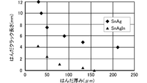
- FIG. 2 shows the results of investigating the relationship between the length of a crack generated in the solder as the bonding material 4 and the thickness of the solder using two types of solder after 300 heat cycle tests.
- the thickness of the solder is preferably set to 100 ⁇ m or more and 300 ⁇ m or less in consideration of generation of cracks, suppression of progress, and heat dissipation. That is, the height of the protrusion 21 is preferably 100 ⁇ m or more and 300 ⁇ m or less.
- the protrusions 21 are positions in the vicinity of the four corners of the arrangement area of the laminated substrate 3 on the main surface of the base plate 2, and are located in the arrangement area more than the position where the semiconductor chip 5 is projected perpendicularly to the main surface of the base plate 2.
- the protrusion 21 is provided at a position about 2 to 10 mm, preferably about 3 to 5 mm inside from the long side and the short side of the arrangement region.
- the protrusion 21 can be formed, for example, by pressing the base plate 2.
- the base plate 2 has a through hole 2a for attaching a heat sink (not shown) to the opposite surface of the main surface with a bolt on the outside of the arrangement region.
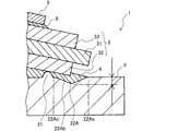
- FIG. 3 shows an enlarged sectional view of the vicinity of the protrusion 21 of the base plate 2.
- a groove 22 ⁇ / b> A is arranged on the outer edge of the arrangement area adjacent to the protrusion 21.
- the groove 22 ⁇ / b> A has an inclination 22 ⁇ / b> Ab corresponding to the inclination due to the warp of the multilayer substrate 3 on the protrusion 21 side in the longitudinal section, and the cross-sectional shape thereof is a triangular shape.
- the groove 22 ⁇ / b> A is filled with the bonding material 4, and the bonding material 4 filling the groove 22 ⁇ / b> A is in contact with the metal plate 32.
- the thickness of the bonding material 4 can be partially increased within the range of the groove 22A. Therefore, even when the multilayer substrate 3 is warped, a desired solder thickness (100 ⁇ m or more) can be secured on the outer edge side of the protrusion 21 of the base plate 2.
- the depth of the groove 22A may be such that the distance from the surface of the metal plate 32 of the laminated substrate 3 to the groove 22A in the vertical direction is 100 ⁇ m or more. Regardless of the degree of warpage of the laminated substrate 3, the depth d of the groove 22 ⁇ / b> A is preferably 100 ⁇ m or more at the maximum depth from the surface of the base plate 2 in order to make the thickness of the bonding material 4 100 ⁇ m or more. However, if the groove 22A exceeds 300 ⁇ m, the effect of suppressing cracks is saturated, and heat dissipation may be deteriorated, which is not preferable. In the groove 22 ⁇ / b> A, the position having the maximum depth is preferably the same as the position when the end of the metal plate 32 of the laminated substrate 3 is vertically projected onto the base plate 2.
- the groove 22A is positioned such that the inner end 22Ac of the main surface of the base plate 2 is outside the semiconductor chip 5 and the protrusion 21. This considers the heat dissipation of the semiconductor chip 5.
- the outer end 22Ae of the groove 22A is located at the same position as the position when the end of the insulating plate 31 of the multilayer substrate 3 is projected onto the base plate 2 perpendicularly, or at the inner side thereof. This is to prevent the groove 22A from interfering with the frame body when the frame body (not shown) is fixed on the base plate 2 outside the arrangement area of the laminated substrate 3 with an insulating adhesive.
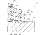
- FIG. 4 is a cross-sectional view of the vicinity of the groove of the base plate 202 in the semiconductor device 201 of the reference example.
- the laminated substrate 203 is configured by laminating a circuit board 233, an insulating plate 231, and a metal plate 232.
- the electrode on the back surface of the semiconductor chip 205 is electrically and mechanically connected to the circuit board 233 by a conductive bonding material 206 such as solder.
- the base plate 202 is provided with a groove 222 having a rectangular cross section.
- the difference from the groove 22A of the present embodiment is that a vertical side surface 222b is provided on the protrusion side instead of the slope 22Ab corresponding to the warp of the laminated substrate.
- a vertical side surface 222b is provided on the protrusion side instead of the slope 22Ab corresponding to the warp of the laminated substrate.
- the thickness of the bonding material 204 in the vicinity of the side surface 222 b is substantially equal to the sum of the height of the protrusion 221 and the depth of the groove 222. Therefore, in the vicinity of the side surface 222b, the bonding material 204 is significantly thicker than a predetermined thickness (that is, the height of the protrusion 21). As a result, at the outer edge of the metal plate 232, heat dissipation from the laminated substrate 3 to the base plate 2 is remarkably deteriorated.
- the groove 22 ⁇ / b> A shown in FIG. 3 is provided with an inclination 22 ⁇ / b> Ab adjacent to the protrusion 21 and corresponding to the inclination due to the warp of the laminated substrate 3.
- the thickness of the bonding material 4 between the metal plate 32 and the base plate 2 can be maintained within a predetermined range.
- the heat dissipation from the laminated substrate 3 to the base plate 2 can be maintained well even at the outer edge of the metal plate 32.
- channel 22A which has inclination 22Ab tends to escape the void which generate
- the groove 222 of the reference example is formed on the base plate 202 by press working, a mold having a substantially right angle (corner) is required.
- this mold has a problem that it is difficult to press and the corners of the mold are easily worn.
- the groove 22A can be formed by press working using a triangular mold having an obtuse angle. This press working is less difficult to process and has a longer die life than the reference example. Therefore, the manufacturing cost can be reduced.
- FIG. 5 is a plan view of the base plate 2 in the first embodiment.
- the grooves 22 ⁇ / b> A are respectively arranged outside the four corners of the arrangement region and surround the four protrusions 21 on the two outer sides.
- channel 22A is arrange
- the bonding material 4 is cracked from the outer edges such as the four corners of the substantially rectangular planar shape and progresses toward the center. Therefore, as shown in FIG. 5, if the grooves 22A of the base plate 2 are arranged in a range including at least the outer edges such as the four corners of the arrangement region, generation and progress of cracks can be effectively suppressed.
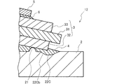
- FIG. 6 is an enlarged cross-sectional view showing Modification Example 1 of the groove in the present embodiment.
- the base plate 2 is provided with a groove 22 ⁇ / b> B adjacent to the protrusion 21 at the outer edge of the arrangement region.
- the groove 22 ⁇ / b> B has an inclination 22 ⁇ / b> Bb corresponding to the inclination due to the warp of the laminated substrate 3 on the protrusion 21 side in the longitudinal section, and the cross-sectional shape thereof is an arc shape.
- FIG. 7 is an enlarged cross-sectional view showing Modification Example 2 of the groove in the present embodiment.
- the base plate 2 has a groove 22 ⁇ / b> C disposed adjacent to the protrusion 21 at the outer edge of the arrangement region.
- the groove 22 ⁇ / b> C has an inclination 22 ⁇ / b> Cb corresponding to the inclination due to the warp of the laminated substrate 3 on the protrusion 21 side in the longitudinal section, and the cross-sectional shape thereof is a trapezoidal shape.
- both the groove 22B and the groove 22C are provided with an inclination corresponding to the inclination due to the warp of the multilayer substrate 3 on the projection 21 side and are not provided with the vertical side surface 222b as in the reference example of FIG.
- the above-mentioned effects shown in the form are provided.
- one laminated substrate 3 is bonded to one base plate 2, but a plurality of laminated substrates 3 may be bonded to one base plate 2.
- FIG. 8 is a plan view of the base plate 2 of the semiconductor device 1 of the second embodiment, and corresponds to FIG. 5 of the first embodiment described above.
- the semiconductor device 1 of the second embodiment has a planar groove 22D different from the groove 22A of the first embodiment.
- the configuration of the other members is the same as that of the semiconductor device 1 of the first embodiment described above.
- the same members as those in FIG. therefore, the description which overlaps with 1st Embodiment is abbreviate
- the base plate 2 has grooves 22 ⁇ / b> D arranged on the outer edge of a predetermined arrangement region of the laminated substrate 3.
- the groove 22 ⁇ / b> D is continuously arranged on the short side of the arrangement area of the multilayer substrate 3, and is arranged on the long side of the arrangement area of the multilayer substrate 3 except for the central portion.
- This embodiment is effective when the convex warpage of the multilayer substrate 3 toward the circuit board 33 is large.
- the amount of displacement on the short side is very large in the planar rectangular laminated substrate 3, and the distance from the base plate 2 is not only near the four corners but also near the center on the short side. Becomes smaller. For this reason, it is important to secure a predetermined solder thickness even in the central portion on the short side.
- the distance between the metal plate 32 and the base plate 2 of the multilayer substrate 3 can be kept at a predetermined distance even in the central portion on the short side. it can.
- a solder thickness will not be increased more than necessary and heat dissipation can be ensured.
- the cross-sectional shape of the groove 22D in the present embodiment is not particularly limited, but can be the same as the groove of the first embodiment described with reference to FIGS.
- the semiconductor device of the present invention has been specifically described with reference to the drawings and embodiments, the semiconductor device of the present invention is not limited to the description of the embodiments and drawings, and does not depart from the spirit of the present invention. Many variations in range are possible.
Landscapes
- Engineering & Computer Science (AREA)
- Mechanical Engineering (AREA)
- Cooling Or The Like Of Semiconductors Or Solid State Devices (AREA)
- Chemical & Material Sciences (AREA)
- Materials Engineering (AREA)
- Insulated Metal Substrates For Printed Circuits (AREA)
Abstract
Description
図9に示す半導体装置101は、金属製のベース板102を備えている。このベース板102は、図示しないヒートシンク(heat sink)にボルトで取り付けるための貫通孔102aを有している。ベース板102上には、積層基板103が接合材104により接合されている。接合材104は、具体的にははんだである。積層基板103は、絶縁板131と、絶縁板131の一方の面に設けられた金属板132と、絶縁板131のもう一方の面に設けられ、所定の回路を形成する回路板133とからなる。積層基板103は一例ではDCB(Direct Copper Bond)基板である。
接合材104をある程度の厚みとするために、ベース板102には、その主面に突起121が配置されている。突起121によりベース板102と金属板132と距離が規制され、突起121の高さと同じ厚みの接合材104が得られる。
図1は、本発明の実施形態1の半導体装置1の断面図(図1(a))及び平面図(図1(b))である。半導体装置1は、積層基板3と、半導体チップ5と、ベース板2と、接合材4を備えている。
また、本実施形態の半導体装置1は、図1に図示しない部材も備えている。例えば半導体チップ5の電極と回路板33とを電気的に接続する配線部材や、回路板33と電気的かつ機械的に接続される外部端子や、半導体チップ5及び積層基板3等を収容する枠体や、枠体の内部空間に充填される封止材等を備えている。
絶縁板31は例えば窒化アルミニウムや窒化珪素、酸化アルミニウム等の絶縁性セラミックスよりなり、金属板32および回路板33は、例えば銅よりなる。絶縁板31及び金属板32は、略長方形の平面形状を有している。そして回路板33は、図示した例では所定の回路パターンが形成された回路板33a、33b、33c、33dを有している。回路板33の沿面距離を確保するために、絶縁板31の長辺及び短辺は共に、金属板32及び回路板33よりも大きい。積層基板3は、これらの絶縁板31と金属板32、回路板33とを直接接合したDCB基板等を用いることができる。
またベース板2は、図示しないヒートシンクを主面の反対面にボルトで取り付けるための貫通孔2aを、配置領域の外側に有している。ヒートシンクにベース板2をボルトで取り付ける際、グリース等を塗布して放熱性を高めているが、グリースが全面に塗り広がるように、ベース板2はヒートシンク側に凸に反らせる場合が多い。このため、回路板33側に凸に反った積層基板3を用いた場合、図1に示すように反りの向きが逆になるため、積層基板3の端部の接合材4の厚みがさらに薄くなりやすい。このため、接合材4のクラックの問題が顕著となる。
しかし、溝22Aが300μmを超えると、クラック抑制の効果が飽和し、また、放熱性が低下するおそれがあるため好ましくない。溝22Aにおいて、最大深さである位置は、積層基板3の金属板32の端をベース板2に垂直に投影したときの位置と同じにすることが好ましい。
ベース板202には断面矩形形状の溝222が設けられている。本実施形態の溝22Aとの違いは、突起側に積層基板の反りに対応した傾斜22Abではなく、垂直な側面222bが設けられている点である。
図4に示した参考例において、側面222bの近傍における接合材204の厚さは、突起221の高さおよび溝222の深さの合計とほぼ等しくなっている。このため、側面222bの近傍においては、接合材204が所定の厚さ(すなわち突起21の高さ)と比べて大幅に厚くなっている。結果として、金属板232の外縁においては、積層基板3からベース板2への放熱性が著しく悪化している。
また、傾斜22Abを有する溝22Aは、垂直な側面222bを有する溝222よりも、接合時に溶融した接合材4の中に発生するボイドが抜け易い。そのため、接合材の信頼性が高く、クラックの発生、進展を更に抑制することができる。
一方、溝22Aは、角が鈍角な三角形状の金型を用いたプレス加工により形成することができる。このプレス加工は、参考例に比べて加工の難易度が低く、また金型寿命も長い。よって、製造コストを低減することができる。
図5に示すように、溝22Aは、それぞれ配置領域の四隅の外側に配置され、4個の突起21を外側の二方で囲んでいる。そして、溝22Aは、配置領域の短辺側及び、配置領域の長辺側にはそれぞれ中央部を除いて配置されている。
なお、図1では、一つのベース板2に一つの積層基板3が接合されているが、一つのベース板2に複数の積層基板3が接合されている構成とすることもできる。
図8を用いて本発明のパワー半導体モジュールの実施形態2について説明する。
図8は、第2実施形態の半導体装置1のベース板2の平面図であり、先に説明した第1実施形態の図5に対応する図面である。第2実施形態の半導体装置1は、第1実施形態の溝22Aとは異なる平面形状の溝22Dを有している。それ以外の部材の構成については先に説明した第1実施形態の半導体装置1と同じである。また、図8において、図5と同一部材については同一の符号を付している。したがって、以下の説明では第1実施形態と重複する記載は省略する。
結果として、本実施形態により、積層基板3の反りが大きくなった場合においても、ベース板2と積層基板3との接合材4にクラックが発生、進展するのを抑制しつつ放熱性を高めることができる。
本実施形態における溝22Dの断面形状は特に限定されないが、図3、図6および図7で説明した第1実施形態の溝と同様とすることができる。
2 ベース板
21 突起
22A、22B、22C、22D 溝
3 積層基板
31 絶縁板
32 金属板
33 回路板
4、6 接合材
5 半導体チップ
Claims (10)
- 回路板、絶縁板及び金属板が積層して構成され、前記回路板側に凸に反った積層基板と、
前記回路板に固定された半導体チップと、
前記積層基板が配置される所定の配置領域と、前記配置領域の外縁に配置された溝と、前記溝に隣接して前記溝よりも前記配置領域の内側に配置された突起を有し、前記溝には前記積層基板の反りによる傾きに対応した傾斜が前記突起側に設けられているベース板と、
前記金属板と前記配置領域との間に充填され、前記溝を埋める接合材と、
を備える半導体装置。 - 回路板、絶縁板及び金属板が積層して構成され、前記回路板側に凸に反った積層基板と、
前記回路板に固定された半導体チップと、
前記積層基板が配置される所定の配置領域と、前記配置領域の外縁に配置された溝と、前記溝に隣接し、前記溝よりも前記配置領域の内側に配置された突起を有し、前記溝は前記配置領域の短辺側には連続して配置され、前記配置領域の長辺側には中央部を除いて配置されるベース板と、
前記金属板と前記配置領域との間に充填され、前記溝を埋める接合材と、
を備える半導体装置。 - 前記溝には、前記積層基板の反りによる傾きに対応した傾斜が前記突起側に設けられている請求項2記載の半導体装置。
- 前記溝は、断面で三角形状、円弧形状、もしくは台形形状である請求項1又は3記載の半導体装置。
- 前記溝の最大深さが、前記ベース板の表面から100μm以上、300μm以下である請求項1又は3記載の半導体装置。
- 前記溝の最大深さである位置は、前記金属板の端を前記ベース板に垂直に投影した位置と同じである請求項1又は3に記載の半導体装置。
- 前記配置領域における前記溝の内側の縁が、前記半導体チップを前記ベース板に垂直に投影した位置よりも外側に位置する請求項1又は3に記載の半導体装置。
- 前記配置領域における前記溝の外側の縁が、前記絶縁板の端を前記ベース板に垂直に投影した位置と同じである請求項1又は3記載の半導体装置。
- 前記配置領域における前記溝の外側の縁が、前記絶縁板の端を前記ベース板に垂直に投影した位置より内側に位置する請求項1又は3記載の半導体装置。
- 前記積層基板は略長方形の平面形状であり、
前記突起は前記配置領域の四隅の近傍にそれぞれ配置されている請求項1又は3記載の半導体装置。
Priority Applications (4)
| Application Number | Priority Date | Filing Date | Title |
|---|---|---|---|
| DE112015000253.7T DE112015000253B4 (de) | 2014-07-18 | 2015-06-05 | Halbleitervorrichtung |
| JP2016534320A JP6191775B2 (ja) | 2014-07-18 | 2015-06-05 | 半導体装置 |
| CN201580004201.1A CN105900231B (zh) | 2014-07-18 | 2015-06-05 | 半导体装置 |
| US15/205,782 US9559035B2 (en) | 2014-07-18 | 2016-07-08 | Semiconductor device |
Applications Claiming Priority (2)
| Application Number | Priority Date | Filing Date | Title |
|---|---|---|---|
| JP2014-148296 | 2014-07-18 | ||
| JP2014148296 | 2014-07-18 |
Related Child Applications (1)
| Application Number | Title | Priority Date | Filing Date |
|---|---|---|---|
| US15/205,782 Continuation US9559035B2 (en) | 2014-07-18 | 2016-07-08 | Semiconductor device |
Publications (1)
| Publication Number | Publication Date |
|---|---|
| WO2016009741A1 true WO2016009741A1 (ja) | 2016-01-21 |
Family
ID=55078244
Family Applications (1)
| Application Number | Title | Priority Date | Filing Date |
|---|---|---|---|
| PCT/JP2015/066386 Ceased WO2016009741A1 (ja) | 2014-07-18 | 2015-06-05 | 半導体装置 |
Country Status (5)
| Country | Link |
|---|---|
| US (1) | US9559035B2 (ja) |
| JP (1) | JP6191775B2 (ja) |
| CN (1) | CN105900231B (ja) |
| DE (1) | DE112015000253B4 (ja) |
| WO (1) | WO2016009741A1 (ja) |
Cited By (5)
| Publication number | Priority date | Publication date | Assignee | Title |
|---|---|---|---|---|
| JP2018006512A (ja) * | 2016-06-30 | 2018-01-11 | 株式会社 日立パワーデバイス | 半導体装置及び移動体 |
| JP2018182174A (ja) * | 2017-04-19 | 2018-11-15 | 富士電機株式会社 | 半導体装置及び半導体装置の製造方法 |
| JP2021125617A (ja) * | 2020-02-07 | 2021-08-30 | 富士電機株式会社 | 半導体装置 |
| US11406005B2 (en) * | 2018-05-29 | 2022-08-02 | Kyocera Corporation | Substrate for mounting electronic element, electronic device, and electronic module |
| JPWO2024241521A1 (ja) * | 2023-05-24 | 2024-11-28 |
Families Citing this family (10)
| Publication number | Priority date | Publication date | Assignee | Title |
|---|---|---|---|---|
| KR102434437B1 (ko) * | 2015-09-17 | 2022-08-19 | 삼성전자주식회사 | 반도체 패키지 |
| DE112016006777B4 (de) * | 2016-04-21 | 2025-08-21 | Mitsubishi Electric Corporation | Halbleitereinheit und Verfahren zur Herstellung derselben |
| JP7184075B2 (ja) * | 2018-03-13 | 2022-12-06 | 住友電気工業株式会社 | 半導体装置 |
| JP7676108B2 (ja) * | 2019-12-06 | 2025-05-14 | 富士電機株式会社 | 半導体装置及び半導体装置の製造方法 |
| JP7120475B2 (ja) * | 2020-01-10 | 2022-08-17 | 富士電機株式会社 | 半導体装置および車両 |
| US11387213B2 (en) * | 2020-06-05 | 2022-07-12 | Advanced Semiconductor Engineering, Inc. | Method for manufacturing a semiconductor package |
| EP3951863A1 (de) * | 2020-08-07 | 2022-02-09 | Siemens Aktiengesellschaft | Kontaktsystem mit zuverlässiger isolierung |
| EP3958302A1 (de) * | 2020-08-17 | 2022-02-23 | Infineon Technologies AG | Bodenplatte für ein halbleitermodul und verfahren zum herstellen einer bodenplatte |
| JP7529038B2 (ja) * | 2020-11-16 | 2024-08-06 | 富士電機株式会社 | 半導体装置及び半導体装置の製造方法 |
| US12424500B2 (en) * | 2021-01-22 | 2025-09-23 | Mitsubishi Electric Corporation | Semiconductor device and method for manufacturing semiconductor device |
Citations (3)
| Publication number | Priority date | Publication date | Assignee | Title |
|---|---|---|---|---|
| JP2002057280A (ja) * | 2000-08-10 | 2002-02-22 | Mitsubishi Electric Corp | 半導体装置 |
| JP2010062203A (ja) * | 2008-09-01 | 2010-03-18 | Shindengen Electric Mfg Co Ltd | 放熱基板ユニット |
| JP2013229363A (ja) * | 2012-04-24 | 2013-11-07 | Daikin Ind Ltd | パワーモジュール |
Family Cites Families (9)
| Publication number | Priority date | Publication date | Assignee | Title |
|---|---|---|---|---|
| JPS60113931A (ja) * | 1983-11-25 | 1985-06-20 | Toshiba Corp | 半導体装置 |
| JPH088373A (ja) * | 1994-06-23 | 1996-01-12 | Toshiba Corp | 放熱装置 |
| JPH1050928A (ja) * | 1996-05-27 | 1998-02-20 | Toshiba Corp | 半導体装置およびその製造方法 |
| JPH10189845A (ja) * | 1996-12-25 | 1998-07-21 | Denso Corp | 半導体素子の放熱装置 |
| US7069645B2 (en) * | 2001-03-29 | 2006-07-04 | Ngk Insulators, Ltd. | Method for producing a circuit board |
| JP2004221256A (ja) * | 2003-01-14 | 2004-08-05 | Auto Network Gijutsu Kenkyusho:Kk | 回路構成体及びその製造方法 |
| JP2005039081A (ja) * | 2003-07-16 | 2005-02-10 | Mitsubishi Electric Corp | 半導体モジュールの放熱板 |
| JP5268994B2 (ja) * | 2010-05-31 | 2013-08-21 | 三菱電機株式会社 | 半導体モジュールとその製造方法 |
| DE102012201172B4 (de) | 2012-01-27 | 2019-08-29 | Infineon Technologies Ag | Verfahren zur Herstellung eines Leistungshalbleitermoduls mit geprägter Bodenplatte |
-
2015
- 2015-06-05 DE DE112015000253.7T patent/DE112015000253B4/de active Active
- 2015-06-05 CN CN201580004201.1A patent/CN105900231B/zh active Active
- 2015-06-05 JP JP2016534320A patent/JP6191775B2/ja active Active
- 2015-06-05 WO PCT/JP2015/066386 patent/WO2016009741A1/ja not_active Ceased
-
2016
- 2016-07-08 US US15/205,782 patent/US9559035B2/en active Active
Patent Citations (3)
| Publication number | Priority date | Publication date | Assignee | Title |
|---|---|---|---|---|
| JP2002057280A (ja) * | 2000-08-10 | 2002-02-22 | Mitsubishi Electric Corp | 半導体装置 |
| JP2010062203A (ja) * | 2008-09-01 | 2010-03-18 | Shindengen Electric Mfg Co Ltd | 放熱基板ユニット |
| JP2013229363A (ja) * | 2012-04-24 | 2013-11-07 | Daikin Ind Ltd | パワーモジュール |
Cited By (6)
| Publication number | Priority date | Publication date | Assignee | Title |
|---|---|---|---|---|
| JP2018006512A (ja) * | 2016-06-30 | 2018-01-11 | 株式会社 日立パワーデバイス | 半導体装置及び移動体 |
| JP2018182174A (ja) * | 2017-04-19 | 2018-11-15 | 富士電機株式会社 | 半導体装置及び半導体装置の製造方法 |
| US11406005B2 (en) * | 2018-05-29 | 2022-08-02 | Kyocera Corporation | Substrate for mounting electronic element, electronic device, and electronic module |
| JP2021125617A (ja) * | 2020-02-07 | 2021-08-30 | 富士電機株式会社 | 半導体装置 |
| JP7459539B2 (ja) | 2020-02-07 | 2024-04-02 | 富士電機株式会社 | 半導体装置 |
| JPWO2024241521A1 (ja) * | 2023-05-24 | 2024-11-28 |
Also Published As
| Publication number | Publication date |
|---|---|
| US9559035B2 (en) | 2017-01-31 |
| CN105900231B (zh) | 2018-09-07 |
| DE112015000253T5 (de) | 2016-11-24 |
| CN105900231A (zh) | 2016-08-24 |
| JP6191775B2 (ja) | 2017-09-06 |
| JPWO2016009741A1 (ja) | 2017-04-27 |
| US20160322274A1 (en) | 2016-11-03 |
| DE112015000253B4 (de) | 2023-06-29 |
Similar Documents
| Publication | Publication Date | Title |
|---|---|---|
| JP6191775B2 (ja) | 半導体装置 | |
| US9362192B2 (en) | Semiconductor device comprising heat dissipating connector | |
| JP7047895B2 (ja) | 半導体装置 | |
| JP6125089B2 (ja) | パワー半導体モジュールおよびパワーユニット | |
| US11348852B2 (en) | Semiconductor device | |
| JP2022000871A (ja) | 電気回路基板及びパワーモジュール | |
| CN111341731A (zh) | 半导体装置 | |
| JP2017139406A (ja) | 半導体装置 | |
| CN111354710B (zh) | 半导体装置及其制造方法 | |
| JP7187814B2 (ja) | 半導体装置 | |
| CN112530915B (zh) | 半导体装置 | |
| JP2015138843A (ja) | 半導体装置及びその製造方法 | |
| JP5693395B2 (ja) | 半導体装置 | |
| JP6907671B2 (ja) | 半導体装置 | |
| US20180308775A1 (en) | Semiconductor device and method of manufacturing same | |
| WO2024185127A1 (ja) | 半導体装置及びその製造方法 | |
| JP2022064488A (ja) | 半導体部品 | |
| JP7831627B2 (ja) | 半導体モジュール | |
| JP7634456B2 (ja) | 半導体装置 | |
| JP6777440B2 (ja) | 回路基板および電子装置 | |
| JP2006286897A (ja) | 金属−セラミックス接合基板 | |
| JP2026081833A (ja) | 半導体装置 | |
| JP6608728B2 (ja) | 回路基板および電子装置 | |
| WO2024095713A1 (ja) | 半導体モジュール及び半導体モジュールの製造方法 | |
| WO2023136074A1 (ja) | 半導体装置 |
Legal Events
| Date | Code | Title | Description |
|---|---|---|---|
| 121 | Ep: the epo has been informed by wipo that ep was designated in this application |
Ref document number: 15822518 Country of ref document: EP Kind code of ref document: A1 |
|
| ENP | Entry into the national phase |
Ref document number: 2016534320 Country of ref document: JP Kind code of ref document: A |
|
| WWE | Wipo information: entry into national phase |
Ref document number: 112015000253 Country of ref document: DE |
|
| 122 | Ep: pct application non-entry in european phase |
Ref document number: 15822518 Country of ref document: EP Kind code of ref document: A1 |