WO2016009467A1 - Dispositif d'analyse à canaux multiples - Google Patents
Dispositif d'analyse à canaux multiples Download PDFInfo
- Publication number
- WO2016009467A1 WO2016009467A1 PCT/JP2014/068657 JP2014068657W WO2016009467A1 WO 2016009467 A1 WO2016009467 A1 WO 2016009467A1 JP 2014068657 W JP2014068657 W JP 2014068657W WO 2016009467 A1 WO2016009467 A1 WO 2016009467A1
- Authority
- WO
- WIPO (PCT)
- Prior art keywords
- channel
- laser beam
- channels
- microchip
- degrees
- Prior art date
Links
Images


Classifications
-
- G—PHYSICS
- G01—MEASURING; TESTING
- G01N—INVESTIGATING OR ANALYSING MATERIALS BY DETERMINING THEIR CHEMICAL OR PHYSICAL PROPERTIES
- G01N21/00—Investigating or analysing materials by the use of optical means, i.e. using sub-millimetre waves, infrared, visible or ultraviolet light
- G01N21/62—Systems in which the material investigated is excited whereby it emits light or causes a change in wavelength of the incident light
- G01N21/63—Systems in which the material investigated is excited whereby it emits light or causes a change in wavelength of the incident light optically excited
- G01N21/64—Fluorescence; Phosphorescence
- G01N21/645—Specially adapted constructive features of fluorimeters
- G01N21/6452—Individual samples arranged in a regular 2D-array, e.g. multiwell plates
- G01N21/6454—Individual samples arranged in a regular 2D-array, e.g. multiwell plates using an integrated detector array
-
- G—PHYSICS
- G01—MEASURING; TESTING
- G01N—INVESTIGATING OR ANALYSING MATERIALS BY DETERMINING THEIR CHEMICAL OR PHYSICAL PROPERTIES
- G01N21/00—Investigating or analysing materials by the use of optical means, i.e. using sub-millimetre waves, infrared, visible or ultraviolet light
- G01N21/01—Arrangements or apparatus for facilitating the optical investigation
- G01N21/03—Cuvette constructions
- G01N21/05—Flow-through cuvettes
-
- B—PERFORMING OPERATIONS; TRANSPORTING
- B01—PHYSICAL OR CHEMICAL PROCESSES OR APPARATUS IN GENERAL
- B01L—CHEMICAL OR PHYSICAL LABORATORY APPARATUS FOR GENERAL USE
- B01L3/00—Containers or dishes for laboratory use, e.g. laboratory glassware; Droppers
- B01L3/50—Containers for the purpose of retaining a material to be analysed, e.g. test tubes
- B01L3/502—Containers for the purpose of retaining a material to be analysed, e.g. test tubes with fluid transport, e.g. in multi-compartment structures
- B01L3/5027—Containers for the purpose of retaining a material to be analysed, e.g. test tubes with fluid transport, e.g. in multi-compartment structures by integrated microfluidic structures, i.e. dimensions of channels and chambers are such that surface tension forces are important, e.g. lab-on-a-chip
-
- G—PHYSICS
- G01—MEASURING; TESTING
- G01N—INVESTIGATING OR ANALYSING MATERIALS BY DETERMINING THEIR CHEMICAL OR PHYSICAL PROPERTIES
- G01N21/00—Investigating or analysing materials by the use of optical means, i.e. using sub-millimetre waves, infrared, visible or ultraviolet light
- G01N21/01—Arrangements or apparatus for facilitating the optical investigation
-
- G—PHYSICS
- G01—MEASURING; TESTING
- G01N—INVESTIGATING OR ANALYSING MATERIALS BY DETERMINING THEIR CHEMICAL OR PHYSICAL PROPERTIES
- G01N21/00—Investigating or analysing materials by the use of optical means, i.e. using sub-millimetre waves, infrared, visible or ultraviolet light
- G01N21/62—Systems in which the material investigated is excited whereby it emits light or causes a change in wavelength of the incident light
- G01N21/63—Systems in which the material investigated is excited whereby it emits light or causes a change in wavelength of the incident light optically excited
- G01N21/64—Fluorescence; Phosphorescence
- G01N21/645—Specially adapted constructive features of fluorimeters
- G01N21/6452—Individual samples arranged in a regular 2D-array, e.g. multiwell plates
-
- B—PERFORMING OPERATIONS; TRANSPORTING
- B01—PHYSICAL OR CHEMICAL PROCESSES OR APPARATUS IN GENERAL
- B01L—CHEMICAL OR PHYSICAL LABORATORY APPARATUS FOR GENERAL USE
- B01L2300/00—Additional constructional details
- B01L2300/08—Geometry, shape and general structure
- B01L2300/0861—Configuration of multiple channels and/or chambers in a single devices
- B01L2300/0877—Flow chambers
-
- B—PERFORMING OPERATIONS; TRANSPORTING
- B01—PHYSICAL OR CHEMICAL PROCESSES OR APPARATUS IN GENERAL
- B01L—CHEMICAL OR PHYSICAL LABORATORY APPARATUS FOR GENERAL USE
- B01L2300/00—Additional constructional details
- B01L2300/16—Surface properties and coatings
- B01L2300/168—Specific optical properties, e.g. reflective coatings
-
- G—PHYSICS
- G01—MEASURING; TESTING
- G01N—INVESTIGATING OR ANALYSING MATERIALS BY DETERMINING THEIR CHEMICAL OR PHYSICAL PROPERTIES
- G01N21/00—Investigating or analysing materials by the use of optical means, i.e. using sub-millimetre waves, infrared, visible or ultraviolet light
- G01N21/62—Systems in which the material investigated is excited whereby it emits light or causes a change in wavelength of the incident light
- G01N21/63—Systems in which the material investigated is excited whereby it emits light or causes a change in wavelength of the incident light optically excited
- G01N21/64—Fluorescence; Phosphorescence
- G01N21/645—Specially adapted constructive features of fluorimeters
- G01N2021/6463—Optics
-
- G—PHYSICS
- G01—MEASURING; TESTING
- G01N—INVESTIGATING OR ANALYSING MATERIALS BY DETERMINING THEIR CHEMICAL OR PHYSICAL PROPERTIES
- G01N21/00—Investigating or analysing materials by the use of optical means, i.e. using sub-millimetre waves, infrared, visible or ultraviolet light
- G01N21/62—Systems in which the material investigated is excited whereby it emits light or causes a change in wavelength of the incident light
- G01N21/63—Systems in which the material investigated is excited whereby it emits light or causes a change in wavelength of the incident light optically excited
- G01N21/64—Fluorescence; Phosphorescence
- G01N21/645—Specially adapted constructive features of fluorimeters
-
- G—PHYSICS
- G01—MEASURING; TESTING
- G01N—INVESTIGATING OR ANALYSING MATERIALS BY DETERMINING THEIR CHEMICAL OR PHYSICAL PROPERTIES
- G01N2201/00—Features of devices classified in G01N21/00
- G01N2201/06—Illumination; Optics
- G01N2201/061—Sources
- G01N2201/06113—Coherent sources; lasers
Definitions
- the present invention relates to a microchip for irradiating a plurality of channels provided in the interior with light such as a laser beam, and analyzing a substance present in the interior by highly sensitively detecting fluorescence, detecting scattered light, and the like, and a manufacturing method thereof , A laser beam irradiation method, and a multi-channel analyzer for analyzing a sample using the microchip.
- Microchip-sized flow channels and reaction tank channels are constructed on the chip, and research and development of microchips that analyze samples of biological materials and the like have been vigorously conducted over the past 20 years, and their practical application is progressing. .
- the microchip is made of transparent glass or resin, and the outer dimensions vary from several millimeters to several tens of centimeters, and the thickness is smaller than the above size. With a microchip, it is possible to analyze a very small amount of sample on the spot in a short time. Examples of microchips already in practical use include PCR, real-time PCR, digital PCR, electrophoretic analysis, immunoassay (immunoassay), flow cytometer (cell sorter), single cell analysis, microreactor, and so on.
- micro TAS Total Analysis System
- Lab on a Chip A microchip that integrates analysis processes including sample introduction, extraction, mixing with reagents, and reactions is called micro TAS (Total Analysis System) or Lab on a Chip.
- a microchip measuring means optical measurement capable of measuring a substance existing inside a channel in a non-contact manner is often used. For example, a fluorescent substance is labeled on a biological substance in a channel, and after removing an unlabeled fluorescent substance, the emitted fluorescence is measured by irradiating a laser beam. Alternatively, the biological material is observed with an optical microscope, and the shape and number thereof are measured.
- Resin microchips can be manufactured by processing techniques such as injection molding and nanoimprinting, and can be mass-produced at low cost, so they can be disposable. Such disposable microchips are particularly important in fields where there is a strong need to avoid contamination other than the sample to be analyzed, such as medical diagnosis and food inspection.
- configuring many channels on a single chip and measuring them in parallel means that if multiple items are analyzed in parallel for a single sample, or if multiple types of samples are measured in parallel, measurement is also possible using these. This is important for improving the throughput of the system and reducing the cost per analysis.
- it is possible to analyze time series changes in reaction and separation by measuring multiple points in a single channel in parallel.
- Beam expansion method A laser beam is expanded and simultaneously irradiated so as to extend over a plurality of channels, and fluorescence from a plurality of channels is detected simultaneously.
- a laser beam is expanded in a line shape and a plurality of channels are simultaneously irradiated.
- a laser beam is expanded in a circular shape or an elliptical shape and a plurality of channels are simultaneously irradiated.
- the laser beam intensity density expands in a circular shape to (1 / N) or less when expanded in a line shape. Then, it decreases to (1 / N 2 ) or less.
- the fluorescence detection sensitivity of each channel decreases.
- the beam expansion method it is conceivable to divide the laser beam into a plurality of beams and irradiate each channel to each channel, but it has the same problem as described above.
- Independent irradiation detection system method A single channel is irradiated with a focused laser beam, and the same number of systems for detecting fluorescence from the same channel are installed for multiple channels. Optimal laser and detection for each channel If a detector can be used, high fluorescence detection sensitivity can be obtained in any channel, but in this case, the cost of the apparatus becomes very high. On the other hand, since a plurality of channels that can be laid out on the same chip must be close to each other, it is physically difficult to provide a highly sensitive laser irradiation fluorescence detection system for each channel. Therefore, it is necessary to adopt a small and low-cost laser irradiation fluorescence detection system that is not relatively sensitive.
- Optical waveguide method By irradiating multiple channels with evanescent waves through an optical waveguide adjacent to multiple channels with evanescent waves and simultaneously detecting fluorescence from multiple channels.
- Evanescent waves can make the laser beam irradiation volume very small By reducing the background light derived from the solution in the channel, it is advantageous, for example, when detecting fluorescence derived from a single fluorescent molecule with high sensitivity.
- the target substance to be detected by the microchip is not such a small number of molecules but a large number of molecules. In such a case, if the laser beam irradiation volume is made too small, the sensitivity decreases.
- Lateral incidence method A laser beam is irradiated from the side of the chip plane along the array plane perpendicular to the long axis of each channel so as to traverse multiple channels. Simultaneous detection of fluorescence With the simplest configuration, the highest sensitivity can be expected. However, since the laser beam is refracted at the interface of each channel, it is difficult to irradiate multiple channels efficiently.
- the center positions of the channels irradiated with the laser beam by the lateral incidence method are aligned on the same straight line. This straight line is hereinafter referred to as a transverse incident axis.
- the transverse incident axis is on the alignment plane and is perpendicular to the long axis of each channel.
- the major axis of each channel is a straight line or a curve passing through the center in the longitudinal direction or the center of gravity of the cross section of each channel.
- the laser beam is irradiated so as to coincide with the transverse incident axis, and a lens or a mirror is inserted between the channels, thereby condensing the laser beam refracted by each channel without deviating from the transverse incident axis. It is possible to penetrate a plurality of channels and to detect fluorescence with high sensitivity.
- the laser beam is made to coincide with the transverse incident axis, the laser beam width is applied to be larger than the channel width, and a plurality of channels are applied simultaneously. When irradiating with the laser beam width wider than the channel width, the laser beam intensity density decreases and the fluorescence detection sensitivity decreases.
- the transverse incidence method which is introduced vertically and penetrates a plurality of channels and simultaneously irradiates a laser beam, is the most efficient laser irradiation fluorescence detection method of a plurality of channels, and is the method that enables the highest sensitivity.
- the lateral incidence method irradiates one channel, and the laser beam that has passed contributes to the irradiation of other channels.
- the central axis of the laser beam when the introduced laser beam goes straight through the plurality of channels without being refracted coincides with the transverse incident axis defined above.
- the lateral incidence method has a very high use efficiency of the laser beam, a very small proportion of the laser beam entering the detector directly or indirectly by reflection, etc. It has such features that the ratio of Rayleigh scattering, Raman scattering, fluorescence, etc. emitted from the chip member by laser beam irradiation to the measurement target fluorescence emitted from the channel is very small. Both contribute to the realization of highly sensitive fluorescence detection with a simple configuration.
- Patent Document 1 a lens or a mirror is inserted between channels, a laser beam that is refracted when passing through the channel and converges to deviate from the horizontal incident axis is collected, and the laser beam is returned to the horizontal incident axis to The horizontal incidence method is realized by passing this channel and repeating this.
- the central axis of the optical system such as a lens must be aligned with an accuracy of micrometer level both in the long axis direction of the channel and in the direction perpendicular to the channel arrangement plane.
- such high-precision alignment must be performed for all of the plurality of lenses arranged between the channels. It is extremely difficult to achieve such positional accuracy only with the mechanical accuracy when a lens is inserted into a hole provided in the microchip. For example, after inserting individual lenses between channels, It is necessary to fine-tune the position and fix it.
- the laser beam is deflected from the horizontal incident axis, so that simultaneous irradiation of a plurality of channels is impossible.
- Such alignment requires labor and time, and requires a separate mechanism for fine adjustment of alignment, leading to an increase in the manufacturing cost of the microchip. This is particularly disadvantageous when the microchip is used disposable.
- the center axis of the laser beam to be introduced is aligned with the center axis of each lens and the position of each lens is fixed to the microchip. It cannot be moved freely in the long axis direction of each channel. This is because if the laser beam is deviated from the central axis of the lens or the like, the laser beam is deflected from the lateral incident axis. This means, for example, that the horizontal incident axis is set avoiding the position where flaws and dust are present in the channel, and cannot be adjusted so as to obtain the highest detection sensitivity.
- a laser beam is expanded in the major axis direction of each channel and incident horizontally, or a plurality of transverse incident axes whose positions are shifted in the major axis direction of each channel are set. Can not be irradiated.
- Patent Document 1 a lens or the like is inserted between the channels, and the positions thereof are aligned with high accuracy. Therefore, it is necessary to increase the distance between adjacent channels, and can be provided in a single microchip. There is a problem that the number of channels is reduced as compared with the conventional (1) beam expansion method and (2) scan method.
- Non-Patent Document 1 in addition to the problem that the laser beam intensity density is reduced by irradiating with the laser beam width wider than the channel width, the laser beam is refracted in one direction by each channel. As the number of channels through which the laser beam passes increases, there is a problem that multiple channels cannot be efficiently irradiated simultaneously because the laser beam rapidly deviates from the transverse incident axis. This is a problem newly found in the present invention, and will be described in detail in [Description of Embodiments].
- the present invention solves the above-mentioned problems of the conventional method of the transverse incidence method, and irradiates a plurality of channels provided on a single microchip simultaneously with the transverse incidence method while having a simple configuration.
- a method for detecting fluorescence with high sensitivity is presented.
- the irradiation position of the laser beam and the transverse incident axis can be moved in the long axis direction of each channel, and the laser beam can be irradiated while being expanded in the long axis direction of each channel, or different laser beams can be irradiated in the length of each channel.
- a method that enables irradiation by shifting the lateral incident axis in the axial direction will be described.
- Microchip members are not only made of glass but also low-priced resins.
- Microchip manufacturing methods are not only time-consuming and costly methods such as cutting, stereolithography, and semiconductor process processing, but also low cost and mass productivity methods such as injection molding and nanoimprint.
- injection molding using a resin material is excellent in low cost and mass productivity, a method for realizing the lateral incidence method while using such a disposable microchip is presented.
- the long axis of each channel is substantially parallel to each other in at least a part of the plurality of channels filled with the member having the refractive index n 2 inside the transparent solid member having the refractive index n 1.
- a microchip arranged on the same plane or on the same cylindrical surface, a laser light source, and a laser beam generated from the laser light source are transmitted from a side surface of the microchip to a plurality of channels arranged substantially parallel to each other. It includes an irradiation optical system that is incident almost perpendicularly to the long axis, and a light detection optical system that separately detects light emitted from multiple channels by laser beam irradiation.
- the direction of the laser beam approaching the target channel is different from the conventional lateral incidence method, and the long axis of the first target channel and the last target are irradiated. Do not make it parallel to the plane containing both the major axes of the channels to be made, but have a certain angle.
- the direction of the laser beam approaching the first irradiated channel is the center of the first irradiated channel and the last irradiated channel center. Make a certain angle without being parallel to the straight line connecting
- the plane coincides with the arrangement plane, and when the centers of the channels are arranged on the same straight line in the cross section, the straight line coincides with the lateral incident axis.
- the direction of the laser beam approaching the first irradiated channel is opposite to the direction in which the laser beam is refracted by each channel.
- the direction of the constant angle is opposite to the direction of the angle at which the laser beam is refracted by each channel.
- the cross section perpendicular to the major axis of the plurality of channels is tapered, and when n 1 > n 2 , the laser beam is directed toward the direction in which the width of the tapered shape increases in the cross section of the channel irradiated first.
- the sign of the certain angle is positive. This makes it possible to increase the distance until the laser beam deviates from the channel arrangement due to refraction caused by each channel, and to simultaneously irradiate more channels efficiently.
- a plurality of laser beams may be provided, and the plurality of laser beams may be incident on different positions in the major axis direction of the plurality of channels.
- the fluorescent substance to be detected is a fluorescent substance labeled on a sample derived from a living body, and fluorescence emitted from a plurality of channels when irradiated with a laser beam is simultaneously emitted from a substantially vertical direction with respect to the upper or lower surface of the microchip. Configure to detect.
- a plurality of channels are arranged in a transparent solid member at least in a partial region, and the long axes of the channels are arranged in parallel on the same plane or the same cylindrical surface.
- a microchip manufacturing method by injection molding the first refractive index n 1 in which a plurality of grooves are formed in parallel to each other in at least a part of the region which is a trapezoidal cross-sectional shape on the surface
- a plate-like transparent solid member, and a second plate-like transparent solid member having a refractive index n 1 are laminated on the first plate-like transparent solid member to form a plurality of channels by a plurality of grooves. It has the process to comprise.
- a laser beam can be efficiently and simultaneously irradiated to a plurality of channels provided in a single microchip by a transverse incidence method.
- the fluorescent substance existing in each channel is excited, and the fluorescence emitted is collectively measured from the vertical direction with respect to the arrangement plane of each channel or the upper or lower surface of the microchip.
- a system that realizes accurate fluorescence detection can be configured.
- the microchip used at this time can be manufactured at low cost by a mass-productive processing method such as injection molding, and the microchip can be made disposable.
- the optical system used for detection can be simplified, and the entire system can be reduced in size and cost.
- Schematic explanatory drawing which shows an example of the multichannel analyzer by this invention. The figure which shows the ray tracing simulation result and irradiation efficiency calculation result of the laser beam which injected transversely into 24 channels arrange
- Explanatory drawing which shows the mechanism which controls the angle which a laser beam and a horizontal incident axis make.
- Explanatory drawing which shows the mechanism which controls the curvature radius of the curved surface which a some channel curve-arranges.
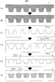
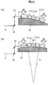
- FIG. 1A is a schematic cross-sectional view showing a typical example of a microchip 1 having an array of a plurality of channels 2 (hereinafter referred to as a channel array).
- 2 is a cross-sectional view including a transverse incident axis 3 (indicated by a dotted line in FIG. 1) of the microchip 1 and perpendicular to the major axes of a plurality of channels 2.
- FIG. The cross section of the microchip 1 is rectangular, and the long side of the rectangle is parallel to the transverse incident axis 3 and the channel arrangement.
- the major axes of the channels 2 are arranged in parallel to each other, on the same plane, and at a constant interval p.
- each channel 2 has No. 1 in order from the left side to the right side where the laser beam is introduced. Number 1, 2, 3, .... In FIG. 1 to 4 are shown. No. The distance between one channel and the left side surface of the microchip 1 is c.
- the cross section of each channel 2 has a tapered shape, here the same isosceles trapezoidal shape.
- the width of each channel 2 in the direction perpendicular to the transverse incident axis 3, that is, the height of the isosceles trapezoid is d.
- the microchip 1 is disposed in a medium having a refractive index n 0 .
- n 0 1.00.
- the member of the microchip 1 is a transparent solid member such as glass or resin, and the refractive index is n 1 .
- the member filled in each channel 2 is a liquid such as an aqueous solution or a gel material, and the refractive index is n 2 and n 2 ⁇ n 1 .
- a macrochip 1 having a channel 2 with an isosceles trapezoidal cross section can be manufactured by using a processing method having excellent mass productivity such as injection molding.
- the microchip 1 is composed of two upper and lower parts having a plane including the upper end surface of each channel 2 as a joint surface 4 (indicated by a one-dot chain line in FIG. 1), and these two parts are bonded together at the joint surface 4 to be integrated. Can be manufactured.
- the upper and lower parts are bonded together by a method such as thermocompression bonding. More preferably, the bonding surface 4 is optically transparent and does not include air or an adhesive layer.
- the joint surface 4 of the component below the joint surface 4 is provided with a plurality of grooves having a square cross section constituting the channel, and the joint surface 4 of the component above the joint surface 4 is a flat surface provided with no groove. is there. For this reason, even if the bonding positions of the upper and lower parts are shifted, the shape and position of each channel 2 are not affected. Injection molding requires a process of drawing a mold after pouring a member such as a resin into the mold, so that the cross-sectional shape of the groove that can be formed is a tapered shape whose width increases from the bottom of the groove toward the joint surface 4 It needs to be.
- the upper base of the isosceles trapezoid is the part of the joint surface 4 and the lower base is the bottom of the groove provided in the part below the joint surface 4, the width of the upper base> the lower base as shown in FIG.
- the process of extracting the mold in a processing method such as injection molding becomes easy, and the mass productivity can be increased.
- the base angle of the isosceles trapezoid the part exceeding 90 degrees is called draft. That is, when the draft is D degrees, the base angle of the isosceles trapezoid is 90 + D degrees.
- the draft D is 0 degree ⁇ D ⁇ 90 degrees, and the larger the D, the easier the process of extracting the mold, but it is desirable that the cross-sectional shape of each channel is uniform, and the smaller the D, the better. In consideration of machining accuracy, it is desirable that D> 2 degrees.
- FIGS. 1B and 1C schematically show optical paths when the laser beam 6 is irradiated on the microchip 1 of FIG. 1A under different conditions.
- the configuration of the microchip 1 and the irradiation condition of the laser beam 6 shown here are only representative examples for explaining the basic idea of the present invention, and other configurations and irradiation conditions based on the same idea are also described in this document. Needless to say, this is the subject of the invention.
- the cross-sectional shape of each channel 2 may not be an isosceles trapezoid, and the arrangement interval may not be constant.
- the laser beam 6 is irradiated from the left side surface of the microchip 1 in a state where the central axis 5 of the laser beam 6 coincides with or is parallel to the transverse incident axis 3. No. 1 before entering the microchip 1 and after entering the microchip 1.
- the width in the direction perpendicular to the arrangement plane of the laser beams 6 until reaching one channel, that is, the width in the direction perpendicular to the transverse incident axis 3 is b in FIG.
- the laser beam 6 is considered to be composed of a large number of infinitesimal beam elements.
- the laser beam 6 is collimated so that the beam elements are substantially parallel, and then the microchip 1 is irradiated. Among these beam elements, No.
- the central axis 5 and the upper and lower beam elements are drawn.
- the central axis 5 is drawn as a representative.
- the isosceles trapezoid which is the cross-sectional shape of each channel 2 can be regarded as a part of the cross section of an isosceles triangular prism, but the refractive index around the prism, that is, the refractive index n 1 of the member of the microchip 1, Since the refractive index of the prism, that is, the refractive index n 2 of the member filled in each channel 2 is smaller, the laser beam incident on the prism is on the opposite side of the base of the isosceles triangle, that is, on the apex angle side. Refract. This problem has been found for the first time in the present invention.
- FIG. 2 is a diagram showing the definition of the refraction angle of the laser beam incident on the isosceles triangular prism, and this phenomenon is schematically shown in an easy-to-understand manner.
- An isosceles triangular prism having a refractive index n 2 and having a cross section of an apex angle A is positioned in the member having the refractive index n 1 with the base side horizontal and the apex angle downward.
- the incident angle at the incident surface is ⁇
- the refraction angle is ⁇
- the incident angle at the exit surface when a virtually zero-width laser beam is horizontally incident on this prism, the incident angle at the incident surface is ⁇ , the refraction angle is ⁇ , and the incident angle at the exit surface.
- ⁇ , ⁇ , ⁇ , and ⁇ all take positive values between 0 ° and 90 °, but ⁇ 2 is ⁇ 90 ° ⁇ 2 ⁇ 90 °, and the sign of the laser beam is as shown in FIG.
- the case where the light is refracted toward the base side is positive, and the case where it is refracted toward the apex angle side is negative.
- ⁇ 2 is a refraction angle received when the laser beam 6 passes through the channel 2.
- the laser beam is refracted to the apex side when passing through the prism, and in FIG. 1B, the laser beam 6 is bonded in a direction away from the transverse incident axis 3 when passing through the channel 2.
- the light is refracted in the direction opposite to the surface 4.
- the central axis 5 of the laser beam 6 is not coincident with or parallel to the transverse incident axis 3, but is inclined by ⁇ 0 (> 0) with respect to the transverse incident axis 3.
- 1 is introduced from the left side, theta 1 with respect to the horizontal axis of incidence 3 (> 0) only inclined No. Irradiate one channel.
- the laser beam 6 is collimated so that the beam elements are substantially parallel, and then the microchip 1 is irradiated.
- the signs of the angles ⁇ 0 and ⁇ 1 are both positive when the laser beam 6 travels in the direction from the lateral incident axis 3 toward the bonding surface 4, that is, in the upper right direction in FIG. To do.
- the signs of the angles ⁇ 0 and ⁇ 1 are positive when the laser beam 6 is directed from the lower part of the microchip 1 provided with the groove toward the upper part without the groove.
- no. In the cross section of the channel No. 1, when the laser beam 6 goes in the direction in which the width of the tapered shape increases, that is, from the narrower side of the tapered shape to the wider side, No.
- the sign of angle ⁇ 1 is positive.
- the refraction angle ⁇ 2 ( ⁇ 0) of each channel increases the distance in the direction of the transverse incident axis 3 until the laser beam 6 deviates from the channel arrangement to the side opposite to the bonding surface 4, and a larger number of channels 2.
- the position where the laser beam 6 is introduced into the left side surface of the microchip 1 is not on the lateral incident axis 3, but is shifted by a (> 0) from the lateral incident axis 3 to the side opposite to the bonding surface 4.
- No. 1 channel can be irradiated well.
- it is important that the magnitude of ⁇ 1 is not too large or too small and is within an appropriate range.
- ⁇ 1 90 degrees, that is, in the case of irradiating the laser beam 6 perpendicularly to the transverse incident axis 3 from bottom to top in FIG.
- the laser beam 6 that has passed through the channel 2 of No. 1 Since it is not possible to irradiate the channels after the second, it cannot be a lateral incidence method, and a plurality of channels cannot be efficiently irradiated simultaneously.
- no. No. 1 channel is irradiated, and the laser beam 6 that has passed through is at least No. 1. It is necessary to illuminate two channels. For this purpose, no.
- the beam element incident on the lower end of the channel No. 1 is No. 1.
- the angle ⁇ 3 formed by the beam element toward 3 to No. 4 is the angle ⁇ 4 formed by the beam element toward the transverse incident axis 3, and (L-1) to No.
- L indicates the total number of channels that are simultaneously irradiated.
- ⁇ 2 , ⁇ 3 , ⁇ 4 ,..., ⁇ L The sign of ⁇ 2 , ⁇ 3 , ⁇ 4 ,..., ⁇ L is the same as that for ⁇ 1 and ⁇ 2 .
- ⁇ 1 , ⁇ 2 , ⁇ 3 , ⁇ 4 ,..., ⁇ L start from positive and eventually turn negative.
- ⁇ 1 to ⁇ 3 are positive, but turn to negative after ⁇ 4 .
- Up to channel 3 is deflected upward, and thereafter, it is deflected downward.
- int (X) is a function for deriving the integer part of X.
- the laser beam 6 is irradiated from the side surface of the microchip 1 as shown in FIG.
- ⁇ 1 according to equation (18) is much larger than ⁇ 1 according to equation (8), so there is no ⁇ 1 compatible with equation (9) or equation (15).
- the present invention inevitably has a configuration in which the laser beam 6 is irradiated from the side surface of the microchip 1 and cannot be applied to the case of irradiation from the lower surface or the upper surface of the microchip 1. This is fundamentally different from the conventional method (1) beam expansion method and (2) beam scan method.
- the configuration shown in FIG. 1C can simultaneously irradiate a larger number of channels 2 by the lateral incidence method as compared with the configuration shown in FIG.
- the number of channels 2 that can be irradiated simultaneously with individual beam elements in the configuration of FIG. 1C is about 2 to 3 times that in the configuration of FIG. 1B.
- the width b of the laser beam 6 is made larger than the width d of each channel 2, first, as shown in FIG. The beam element irradiating the channel 2 of No.
- the width b of the laser beam 6 suitable for realizing an efficient lateral incidence method depends on the total number L of channels 2 to be simultaneously irradiated.
- L does not necessarily match the total number of channels 2 included in the microchip 1. If there are beam elements that irradiate each of the L channels 2 first, all L channels 2 can be irradiated simultaneously.
- the width of the laser beam 6 incident from the left side surface of the microchip 1 in the direction of the transverse incident axis 3 is 1 channel 2 and no.
- the distance of channel 2 of L should be larger than p ⁇ (L ⁇ 1), and the condition is b> p (L ⁇ 1) tan ⁇ 1 (19) It is.
- Equation (19) a condition for simultaneously irradiating all L channels 2 more efficiently while reducing the size of b from Equation (19).
- the number of channels 2 that can be irradiated simultaneously by the individual beam elements in the configuration of FIG. 1C is twice that of the configuration of FIG. 1B as a typical example
- the number of channels 2 can be calculated using equation (14). Can be expressed as 2 ⁇ M ⁇ 1.
- M is assumed.
- the effect of enlarging the width d in the vertical direction has been described.
- the width in the direction parallel to the arrangement plane of the laser beams 6, that is, the width in the major axis direction of each channel 2 is not subjected to the same enlargement. Many. There are two reasons for this.
- each channel 2 is analyzed by laser beam irradiation and fluorescence detection, the laser beam width in the major axis direction of each channel 2 becomes larger than the width of each channel 2. Electrophoretic resolution is reduced. The other is that if the laser beam 6 is expanded not only in the direction perpendicular to the arrangement plane but also in the parallel direction, the laser beam intensity density is reduced by that amount, so that the irradiation efficiency and fluorescence detection sensitivity of each channel 2 are reduced. It is because it ends up.
- the laser beam 6 is expanded only in the direction perpendicular to the arrangement plane, that is, the microchip 1 and each channel are shaped so that the cross section of the laser beam 6 is elliptical or linear. 2 is good.
- the direction of measuring scattered light or fluorescence from each channel 2 by irradiation with the laser beam 6 may be from above or below the microchip 1 in FIG. That is, even if FIG. 1 is turned upside down, the contents of the above invention are not affected.
- the center axis of the light detection system is perpendicular to at least one of the arrangement plane of the channels 2, the upper surface or the lower surface of the microchip 1. It is good for improving sensitivity and reducing variations.
- ⁇ 0 , ⁇ 1 , ⁇ 2 ,..., ⁇ L are defined as angles that form the transverse incident axis 3 of the laser beam 6 or the array plane, but these angles are perpendicular to the central axis of the light detection system. It may be defined as an angle with respect to a simple plane.
- FIG. 3 is a process diagram showing a cross-sectional schematic view of a process for manufacturing the microchip 1 shown in FIG. 1 by injection molding.
- a member in which a transparent resin is heated and melted as shown in (b) is injected and injected into the mold 7 shown in (a), and cooled and solidified.
- a component 8 having a plurality of grooves to be channels of the microchip 1, that is, a component 8 below the bonding surface 4 of the microchip 1 is obtained as shown in FIG.
- the member of the component 8 is a transparent solid member having a refractive index n 1 .
- the component 8 is obtained by forming a plurality of grooves having a trapezoidal cross-sectional shape on the surface of a plate-like transparent solid member. The grooves are arranged in parallel to each other in at least some areas.
- a plate-like transparent solid member having a refractive index n 1 is separately produced as a component 9 that does not have a channel of the microchip 1, that is, a component 9 above the bonding surface 4 of the microchip 1. and, bonding by thermal welding or the like at the joining surface 4 and part 8, (e), the obtaining microchip 1 of refractive index n 1. That is, by this process, a plurality of channels 2 are formed inside the microchip 1 by a plurality of grooves formed on the surface of the component 8. In this state, the interior of each channel 2 is filled with air.
- a plurality of channels 2 are filled with a medium having a refractive index n 2 used for analysis, thereby producing channels 2.
- the microchip 1 is distributed to users in the state (e) or (f), for example. Since the component 9 has a flat surface, it may have a flexible thin sheet shape, for example, a thickness of about 100 ⁇ m. Thus, making the component 9 into a thin sheet shape contributes to reducing the manufacturing cost of the microchip 1. In the present invention, the direction in which the laser beam 6 is refracted is away from the joint surface 4, so that there is no particular problem caused by the thickness of the component 9 being reduced.
- the same effect can be obtained even if the cross-sectional shape of the channel 2 is other than the trapezoid.
- At least the cross-sectional shape of the channel 2 that can be manufactured by a processing method such as injection molding or nanoimprinting is an object.
- the same effect can be obtained even if the trapezoid, triangle, or each side of the trapezoid or triangle is not a straight line but is arcuate, or the corners of the trapezoid or triangle are rounded.
- D the case of such a general cross-sectional shape, it can be considered that the above relational expression is established by obtaining D as follows.
- the minimum value of the width parallel to the transverse incident axis of the cross-sectional shape of each channel is W min
- the maximum value is W max
- the maximum value of the width perpendicular to the transverse incident axis is d.
- W min is obtained at a position farthest from the joint surface
- W max is obtained at a position closest to the joint surface.
- D 90 ⁇ tan ⁇ 1 ⁇ 2d / (W max ⁇ W min ) ⁇ .
- FIG. 4 is a schematic cross-sectional view of a microchip including a plurality of channels showing another solution.
- the center positions of the channels 2 irradiated with the laser beam are arranged on the same straight line, that is, on the horizontal incident axis 28 without being arranged on the horizontal incident axis 3.
- the channel arrangement is not on the plane including the lateral incident axis 3 but on the curved surface including the lateral incident curve 28. That is, the long axes of the plurality of channels 2 are arranged on a cylindrical surface having a radius of curvature R.
- the plurality of channels have a tapered shape (here, an isosceles trapezoidal shape) in a cross section perpendicular to the long axis.
- the laser beam 6 transmitted through the channel 2 of No. 1 is No. 1. No. 1 due to the refraction action by channel 2. It advances at an angle of ⁇ 2 with respect to the laser beam 6 before entering the channel 2 of 1. Therefore, the central axis 5 is No. No. 2 is parallel to the upper and lower bases of the isosceles trapezoid that is the cross section of the channel 2, and No.
- the joint surface 4 is also curved in the same manner as the lateral incidence curve 28.
- the transverse incidence curve 28 is curved in the same direction as the direction in which the laser beam 6 is refracted by each channel 2. That is, when the upper base> the lower base in the isosceles trapezoidal shape of the cross section of the channel 2, the lateral incident curve 28 is curved in the direction from the upper base to the lower base.
- the transverse incidence curve 28 is curved in the opposite direction from the center of the channel 2 toward the bonding surface 4 of the microchip 1.
- the radius of curvature R indicating the degree of curvature is preferably constant regardless of the position when the arrangement interval p of the channels 2 is constant.
- the arrangement position of the channels 2 is curved with a constant curvature radius R over a region where the plurality of channels 2 to be measured are arranged.
- the upper and lower surfaces of the microchip 1 are No. 1 is parallel to the direction of the laser beam 6 before entering the channel 2, and the left side surface and the right side surface of the microchip 1 are No. 1.
- the direction in which scattered light or fluorescence from each channel 2 due to the irradiation of the laser beam 6 is measured may be from above or below the microchip 1 in FIG. That is, even if FIG. 4 is turned upside down, the contents of the above invention are not affected.
- Making the central axis of the light detection system perpendicular to the plane including both of the long axes of the L channels 2 can improve the light detection sensitivity of each channel 2 and reduce variations.
- FIG. 5 is a schematic explanatory diagram showing an example of a multi-channel analyzer according to the present invention.
- This embodiment shows a system for performing electrophoretic analysis of DNA contained in a biological sample, (a) is a bird's-eye view of the microchip 1, and (b) is a transverse incident axis 3 of a laser beam 6 with respect to the microchip 1 constituting the system.
- a cross section of the fluorescence detection optical systems 13 to 16, and the data analysis device 17, and (c) shows a two-dimensional fluorescence image 18 obtained by the two-dimensional sensor 16.
- Laser scattered light and fluorescence wavelength dispersion images 19 from each channel 2 due to excitation of the laser beam 6 are measured independently of each other.
- the medium 0 of refractive index n 0, are arranged microchip 1 is composed of members of the refractive index n 1, members of the refractive index n 2 in the microchip 1
- a plurality of channels 2 filled with are arranged.
- Each channel 2 is provided with an inlet port 10 and an outlet port 11 common to each channel 2.
- Each of the channels 2 in the vicinity of the inlet port 10 is provided with a cross injection part or a double T injection part for introducing a sample, which is omitted in FIG.
- a region of interest is amplified in advance and a fluorescent substance is labeled.
- each channel 2 After the sample is introduced, by applying a voltage to both ends of each channel 2 with the inlet port 10 as the negative electrode and the outlet port 11 as the positive electrode, the fluorescently labeled DNA contained in the sample is electrophoretically separated from the inlet port 10 toward the outlet port 11.
- the plurality of channels 2 are arranged such that the long axes of the channels are substantially parallel to each other in at least a part of the region.
- the laser beam generated from the laser light source is incident from the side surface of the microchip substantially perpendicularly to the long axes of a plurality of channels arranged substantially parallel to each other.
- the laser beam 6 emitted from the laser light source 12 is stopped by an irradiation optical system including a lens, introduced from the side surface of the microchip 1, and each channel 2 is irradiated.
- 5A and 5B for simplicity, the center axis 5 of the laser beam 6 introduced into the microchip 1 and the lateral incident axis 3 are expressed as being coincident or parallel, but it is accurate. As described above and as will be described later with reference to FIG. 21, these have a significant angle.
- the fluorescently labeled DNA that is electrophoresed in each channel 2 is excited by the laser beam 6 when it crosses the position where the laser beam 6 is irradiated, and emits fluorescence.
- the fluorescence emitted from each channel 2 is detected by a fluorescence detection optical system. That is, the light is collimated by the common condenser lens 13, passes through the filter and the diffraction grating 14, and is imaged on the sensor surface of the two-dimensional sensor 16 by the imaging lens 15.
- the filter is provided in order to block the wavelength of the laser beam 6 which becomes background light in fluorescence detection
- the diffraction grating is provided in order to detect the multicolor by wavelength dispersion of the fluorescence. Since the cross section of the channel 2 has the same shape with respect to the long axis direction of the channel 2, the same effect can be obtained even if the incident position of the laser beam 6 on the microchip 1 is slightly shifted in the long axis direction of the channel 2. Is obtained and the fluorescence detection sensitivity is not affected.
- FIG. 5C is a schematic diagram showing a two-dimensional fluorescent image 18 obtained by the two-dimensional sensor 16.
- the direction of chromatic dispersion is the long axis direction of each channel 2 (the direction perpendicular to the cross-sectional view of FIG. 5B), that is, the direction perpendicular to the arrangement direction of the plurality of channels 2.
- the chromatic dispersion images are measured independently without overlapping each other.
- a laser light scattering and fluorescence wavelength dispersion image 19 that cannot be completely removed by the filter is obtained.
- the fluorescence signal thus measured is analyzed by the data analyzer 17 and the sample introduced into each channel 2 is analyzed.
- FIG. 21 is a schematic cross-sectional view showing in detail the laser beam 6, the microchip 1 and the plurality of channels 2 shown in FIG. 5, and shows a mechanism for controlling the angle formed between the laser beam and the transverse incident axis. It is explanatory drawing.
- the microchip 1 and the analyzer are simply installed on the stage 27 of the analyzer. It is desirable that the parameters defined above, such as the angle ⁇ 1 of the laser beam 6 irradiated to one channel 2 with respect to the transverse incident axis 3, are designed to have desired values. However, it is assumed that ⁇ 1 and the like deviate from the designed values due to variations in processing accuracy of the microchip 1, deformation due to deterioration, or deformation due to environmental factors of the analyzer.
- FIG. 21A shows an example of a calibration mechanism.
- the irradiation angle of the laser beam 6 with respect to the microchip 1 becomes a desired angle ⁇ 1.
- FIG. 21B the position and angle of the stage 27 are controlled by the adjustment mechanism 26 so that a desired angle ⁇ 1 can be obtained.
- the adjustment mechanism of FIG. 21A and the adjustment mechanism of FIG. 21B may be used in combination.
- the relative angle between the laser beam 6 and the microchip 1 is adjusted by the adjusting mechanism 26 in FIG. 21 (a) or FIG. 21 (b). It is effective to adjust the signal intensity so that the signal intensity approaches the design value. It is convenient to use the Raman scattering intensity of water obtained from each channel 2 as the signal intensity. It is also effective to incorporate a calibration marker in advance inside the microchip 1 separately from the channel 2 used for sample analysis. For example, as shown in FIG. 24A, calibration channels 31 are provided on both sides of the array of channels 2 used for analysis. The channel 31 is filled with a medium having a refractive index n 2 and a relatively strong Raman scattering, similar to the channel 2.
- the adjusting mechanism 26 shown in FIG. 21A or 21B is controlled to obtain an appropriate relative angle. Furthermore, since the light emission from the channel 31 can be measured simultaneously and independently with the light emission from the channel 2 by the fluorescence detection optical system shown in FIG. 5B, the adjustment mechanism 26 is controlled in real time while analyzing. You can also. This is effective as a countermeasure when the microchip is deformed due to a temperature rise or the like during the analysis.
- a ray tracing simulation of the laser beam 6 incident on the plurality of channels 2 provided on the microchip 1 is performed, and the laser beam 6 before being incident incident on the microchip 1 is performed.
- the ratio of the intensity of the laser beam 6 passing through the inside of each channel 2 to the total intensity of the laser beam, that is, the laser beam irradiation efficiency for each channel 2 is obtained, and how many channels can be incident laterally with what efficiency. evaluated. It has been proved that the laser beam irradiation efficiency for each channel 2 obtained from such ray tracing simulation agrees well with the fluorescence intensity ratio for each channel 2 obtained in the experiment, as shown in known literature. , It is an extremely reliable evaluation method.
- the lighting design analysis software LightTool TM (Synopsys' Optical Solutions Group) is used as a three-dimensional ray tracing simulator.
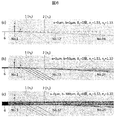
- FIGS. 6, 8, 10, 12, 14, and 16 show the results of ray tracing simulation.
- the wavelength of the laser beam 6 is 505 nm.
- no. 1 to No. A total of 24 24 channels 2 are arranged on the same plane. That is, L 24.
- Reference numeral 1 denotes an end on the side where the laser beam 6 is introduced, and indicates the number of the channel 2 to which the laser beam 6 is first irradiated. Thereafter, in order of each channel 2 along the traveling direction of the laser beam 6, 2, no. 3, ... No. Number 24.
- Each figure is represented by a yz plane consisting of a y-axis and a z-axis. The center of the channel 1 of 1 and the z axis are aligned with the transverse incident axis 3.
- the member of the microchip 1 was ZEONOR TM (Zeonor, Nippon Zeon).
- ZEONOR is a cycloolefin polymer (COP) resin, and is often used as a microchip member due to its high transparency and low hygroscopicity.
- each channel 2 was the same isosceles trapezoid.
- the cross-sectional shape of the channel 2 is an isosceles trapezoid is to improve the mass productivity of the microchip 1 as described above.
- the surface including the upper base of each isosceles trapezoid is the joint surface 4.
- the laser beam 6 is composed of 300 infinitely small beam elements, and the positions of these beam elements are uniform and random within the respective diameters (a), (b), and (c) of each figure. Arranged. Further, the total intensity of the laser beam 6 before entering the microchip 1 is set to 1.00 (100%), and each beam element is equally given an intensity of 1/300 (0.33%). . In the ray tracing simulation, Snell's law is applied at each position where the refractive index changes, such as the entrance surface to the microchip 1, the entrance surface to each channel 2, and the exit surface from each channel 2 for each beam element. And the direction and intensity of refracted light were traced by applying Fresnel's law. However, when the beam element was totally reflected at the position where the refractive index changed, the traveling direction and intensity of the reflected light were tracked. Each figure shows the optical path of 300 beam elements thus calculated.
- the buffer solution was filled in each channel 2.
- the laser beam irradiation efficiency is No. Channel 2 of 1 is the same as that of FIG. No. 1 monotonically decreases in channel 2 and later. It became zero in channel 2 after 7.
- the condition of b 300 ⁇ m in FIG. 6C is a typical example in the case where the laser beam 6 is laterally incident with a diameter larger than that of the channel 2. No. Since there are many beam elements that do not contribute to irradiation in all the channels 2 after 1 and the effective laser beam intensity is reduced by that amount, the laser beam irradiation efficiency in FIG. In case of (b), it is reduced to about 1/5. It became zero in channel 2 after 7. In FIG.
- Expression (16) is satisfied.
- the condition that satisfies the equation (17) is ⁇ 1 > 0.52 degrees, and the equation (17) is also satisfied.
- the condition that satisfies the equation (9) is ⁇ 1 ⁇ 10.00 degrees, and the equation (9) is also satisfied.
- the condition that satisfies Expression (15) is ⁇ 1 ⁇ 3.46 degrees, and Expression (15) is not satisfied.
- the other conditions and display methods of FIGS. 8 and 9 are the same as those of FIGS.
- FIG. 8A shows the irradiation of more channels 2 as compared with FIG. 6A as a result of the increased distance in the direction of the transverse incident axis 3 until the laser beam 6 deviates from the channel 2 arrangement. It shows that it contributes to.
- Irradiation of 11 channels 2 of 1 to 11 is possible, and the number of channels that can be irradiated at the same time is greatly increased as compared with the four channels of FIG.
- the average value of the laser beam irradiation efficiency decreases and the variation increases.
- 8 (b) and 9 (b) show that the number of channels that can be irradiated simultaneously has increased from 6 to 11 compared to FIGS. 6 (b) and 7 (b) due to the same effect. It shows that.
- ⁇ 1 > 0.00 degrees in equation (16) ⁇ 1 > 0.52 degrees in equation (17), ⁇ 1 ⁇ 10.00 degrees in equation (9), ⁇ 1 ⁇ 3.46 degrees is all satisfied.
- more efficient laser beam lateral incidence can be realized as compared with the cases of FIGS.
- FIGS. 10 (a) and 11 (a) compared to FIGS. 8 (a) and 9 (a), the condition (15) is satisfied, so that the condition for the more lateral incidence is obtained, and simultaneous irradiation is performed.
- the number of possible channels is reduced from 11 to 9, the average value of the laser beam irradiation efficiency is greatly improved and the variation is greatly reduced.
- FIG. 10B and FIG. 11B the number of channels that can obtain a laser beam irradiation efficiency of 70% or more as compared with FIG. 8B and FIG. It has increased from seven to seven. This is an important performance for performing highly sensitive analysis in a large number of channels.
- a microchip provided with a plurality of channels each having an isosceles trapezoidal cross section perpendicular to the major axis is used, and the laser beam is tilted from the side surface of the microchip by ⁇ 1 > 0 with respect to the transverse incident axis.
- the channel whose cross-sectional shape perpendicular to the long axis is an isosceles trapezoid has been described as an example.
- the cross-section is triangular, or each side is not a straight line but an arc.
- the same effect can be obtained.
- the same effect can be obtained for a microchip provided with a plurality of channels each having a tapered shape with a cross section perpendicular to the major axis widening toward the end.
- the laser beam 6 is not necessarily introduced from the upper surface or the lower surface of the microchip 1, but is introduced from the side surface of the microchip 1.
- Example 2 In the present embodiment, the difference from the first embodiment will be mainly described, and if there is no particular description, it may be considered that the same description as in the first embodiment holds.
- the member filled in each channel 2 was changed from a buffer solution to a 3500/3500 ⁇ L POP-7 TM polymer solution (Life Technologies).
- POP-7 is an aqueous solution containing 8M urea and a polymer as an electrophoretic separation medium, and is used for DNA sequencing.
- Expression (16) is satisfied.
- the condition that satisfies the equation (17) is ⁇ 1 > 0.31 degrees, and the equation (17) is also satisfied.
- the condition that satisfies the equation (9) is ⁇ 1 ⁇ 9.74 degrees, and the equation (9) is also satisfied.
- the condition that satisfies Expression (15) is ⁇ 1 ⁇ 2.68 degrees, and Expression (15) is not satisfied.
- FIGS. 14A and 14B the central axis 5 of the laser beam 6 is No.
- FIG. 14C the vicinity of the upper end of the laser beam 6 is No. 1 channel 2 was irradiated.
- Other conditions, display methods, and the like in FIGS. 14 and 15 are the same as those in FIGS. 12 and 13.
- FIG. 14A shows the irradiation of more channels 2 as compared with FIG. 12A as a result of increasing the distance in the direction of the transverse incident axis 3 until the laser beam 6 deviates from the channel 2 arrangement. It shows that it contributes to.
- FIG. It is possible to irradiate 14 channels 2 of 1 to 14, and the number of channels that can be irradiated at the same time is greatly increased as compared with 6 channels in FIG.
- the average value of the laser beam irradiation efficiency decreases and the variation increases.
- 14 (b) and 15 (b) show that the number of channels that can be irradiated simultaneously has increased from 8 to 14 compared to FIGS. 12 (b) and 13 (b) due to the same effect. It shows that.
- the effect is particularly high in that the number of channels capable of obtaining a laser beam irradiation efficiency of 30% or more is increased from 6 to 13.
- the effect is particularly high in that the number of channels capable of obtaining a laser beam irradiation efficiency of 30% or more is increased from 0 to 16.
- ⁇ 1 ⁇ 9.74 degrees in equation (9) All ⁇ 1 ⁇ 2.68 degrees are satisfied. This makes it possible to realize a more efficient laser beam lateral incidence as compared with the cases of FIGS.
- the position where the central axis 5 of the laser beam 6 is incident on the side surface of the microchip 1 is lower than the lateral incident axis 3, that is, away from the bonding surface.
- the other conditions, display methods, and the like in FIGS. 10 and 11 are the same as those in FIGS.
- FIG. 16A and FIG. 17A compared with FIG. 14A and FIG. 15A, the condition (15) is satisfied, so that the conditions suitable for further lateral incidence are obtained.
- the number of possible channels is only 11, the average value of the laser beam irradiation efficiency is greatly improved and the variation is greatly reduced.
- FIG. 16B and FIG. 17B the number of channels that can obtain a laser beam irradiation efficiency of 70% or more as compared with FIG. 14B and FIG. The number has increased from nine to nine. This is an important performance for performing highly sensitive analysis in a large number of channels.
- 16C and 17C show an average value of the laser beam irradiation efficiency for 24 channels 2 from 32% to 18% as compared with FIGS. 14C and 15C.
- a microchip provided with a plurality of channels each having an isosceles trapezoidal cross section perpendicular to the major axis is used, and the laser beam is tilted from the side surface of the microchip by ⁇ 1 > 0 with respect to the transverse incident axis.
- the channel whose cross-sectional shape perpendicular to the long axis is an isosceles trapezoid has been described as an example.
- the cross-section is triangular, or each side is not a straight line but an arc.
- the same effect can be obtained.
- the same effect can be obtained for a microchip provided with a plurality of channels each having a tapered shape with a cross section perpendicular to the major axis widening toward the end.
- the laser beam 6 is not necessarily introduced from the upper surface or the lower surface of the microchip 1, but is introduced from the side surface of the microchip 1.
- Example 3 shows a system for performing electrophoretic analysis of DNA contained in a biological sample, where (a) is a bird's-eye view of the microchip 1 and (b) is lateral incidence of the laser beam 6 and the laser beam 20 of the microchip 1.
- the medium 0 of refractive index n 0, are arranged microchip 1 is composed of members of the refractive index n 1, members of the refractive index n 2 in the microchip 1
- a plurality of channels 2 filled with are arranged.
- Each channel 2 is provided with an inlet port 10 and an outlet port 11.
- a laser beam 6 having a wavelength of 505 nm and a laser beam 20 having a wavelength of 635 nm are introduced from the side surface of the microchip 1 and the array of channels 2 is irradiated by transverse incidence. ing.
- the laser beam 6 and the laser beam 20 irradiate a position shifted in the major axis direction of each channel 2, that is, the lateral incident axis 3 and the lateral incident axis 21, respectively. Since the conditions such as the cross-sectional shape of each channel, the arrangement interval, the refractive index, and the like are the same for any transverse incident axis, an equivalent transverse incidence method can be realized. In general, since the refractive index of each member varies depending on the wavelength, it may affect the performance of the lateral incidence method. However, since the wavelength dependency of the refractive index of each member used in the present invention is small, the influence is small.
- the laser beam 6 and the laser beam 20 are each divided into two and then irradiated from both side surfaces of the microchip 1.
- the use of a plurality of types of laser beams and the introduction of each laser beam from both sides of the microchip may be performed simultaneously as described above, or of course only one of them.
- Other structures of the microchip 1 and irradiation conditions of the laser beams 6 and 20, for example, the laser beam width b perpendicular to the array plane and the transverse incident axis, and the angle ⁇ 1 between the central axis of the laser beam and the transverse incident axis are implemented. Equivalent to any of the conditions shown in Example 1 or Example 2.
- the laser beams 6 and 20 emitted from the laser light sources 12 and 22 are irradiated from both side surfaces of the microchip 1 after being divided into two by using the half mirror 23 and the mirror 24.
- the central axis of the laser beam 6 and the laser beam 20 introduced into the microchip 1 and the lateral incident axis 3 and the lateral incident axis 21 are respectively coincident or parallel to each other.
- they have a significant angle.
- the fluorescently labeled DNA that is electrophoresed in each channel 2 is excited when it crosses the position where the laser beam 6 and the laser beam 20 are irradiated, and emits fluorescence.
- the fluorescence emitted from each channel 2 is detected by the fluorescence detection optical systems 13-16. That is, the light is collimated by the common condenser lens 13, passes through the filter and the diffraction grating 14, and is imaged on the sensor surface of the two-dimensional sensor 16 by the imaging lens 15.
- the filter is provided to block the wavelengths of the laser beam 6 and the laser beam 20 which are background light at the time of fluorescence detection, and the diffraction grating is provided for multi-color detection by wavelength dispersion of fluorescence.
- FIG. 18C is a schematic diagram showing a two-dimensional fluorescent image 18 obtained by the two-dimensional sensor 16.
- the direction of chromatic dispersion is the long axis direction of each channel 2 (the direction perpendicular to the cross-sectional view of FIG. 18B), that is, the direction perpendicular to the arrangement direction of the plurality of channels 2.
- the laser light scattering and fluorescence wavelength dispersion image 19 from 2 and the laser light scattering and fluorescence wavelength dispersion image 25 from each channel 2 by excitation of the laser beam 20 are measured independently. With the above configuration, it is possible to identify a small amount of fluorescence by increasing the number of types of fluorescence that can be simultaneously detected in each channel 2 or by separating and detecting different fluorescence with high accuracy. In this example, different samples were labeled with different phosphors and analyzed simultaneously in the same channel to improve throughput.
- FIG. 25 shows the effect when the laser beam 6 is divided into two parts and irradiated from both side surfaces of the microchip 1. As shown below, laser beam irradiation from both sides increases the number of channels 2 that can be irradiated simultaneously, and reduces variations in laser beam irradiation efficiency between channels 2 to obtain uniform fluorescence detection sensitivity. It is an effective means.
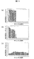
- FIG. 19 shows the laser beam irradiation efficiency in each channel 2 when the number is reduced from 16 to 16 and the laser beam 6 is divided into two according to FIG. 18 and irradiated from both side surfaces of the microchip 1.
- one of the two divided laser beams 6 is No. 1 from the side surface of the microchip 1 as in FIG. 1 channel 2 is irradiated, and the other is No. 1 from the opposite side of microchip 1.
- 16 channels 2 are irradiated. No. 1 and no.
- the two divided laser beams 6 that respectively irradiate the 16 channels 2 are in the center of the channel arrangement, that is, No. 1. 8 and no. 9 is made to be symmetric with respect to a plane passing through the midpoint of the channel 2 and perpendicular to the transverse incident axis 3.
- the total number of channels 2 that can be irradiated simultaneously is 10
- the laser beam irradiation efficiency of these 10 channels 2 is 65% on average
- the standard deviation is 26%
- the CV value is 40%.
- the total number of channels 2 that can be irradiated simultaneously increases to 16, and the laser beam irradiation efficiency of these 16 channels 2 is an average of 41%, which is slightly small. Uniform irradiation is possible between channels with a deviation of 5% and CV value of 12%.
- FIG. 19 shows the laser beam irradiation efficiency in each channel 2 when the number is reduced from 20 to 20 and the laser beam 6 is divided into two according to FIG. 18 and irradiated from both side surfaces of the microchip 1. Similarly, no. 1 and no. The two divided laser beams 6 irradiating each of the 20 channels 2 are in the center of the channel arrangement, that is, No. 10 and no. 11 is symmetric with respect to a plane passing through the midpoint of the channel 2 and perpendicular to the transverse incident axis 3.
- the total number of channels 2 that can be irradiated simultaneously is 12
- the laser beam irradiation efficiency of these 12 channels 2 is 70% on average, 26% standard deviation, and 37% CV value.
- the total number of channels 2 that can be irradiated simultaneously is increased to 20, and the laser beam irradiation efficiency of these 20 channels 2 is an average 42%, which is a little small. Uniform irradiation is possible between channels with a deviation of 2% and CV value of 6%.
- the microchip 1 in which the channel arrangement is curved can be manufactured by any method.
- One manufacturing means is to design a mold in advance so that a desired radius of curvature can be obtained at the stage of manufacturing the parts of the microchip 1 below and above the joint surface 4 in FIG. 4 by injection molding. It is. In this way, the curved surface is excellent at injection molding, and it is also easy to join two parts having the same radius of curvature by thermocompression bonding or the like.
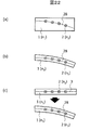
- FIG. 22 is a schematic cross-sectional view of the microchip 1 in which a plurality of channels 2 are curvedly arranged on an arc having a desired radius of curvature, that is, on a lateral incidence curve 28.
- the microchip shown in FIG. 22A is an example in which the upper surface and the lower surface of the microchip 1 are parallel to the laser beam 6 introduced into the microchip 1 as in FIG.
- Such a microchip 1 can be easily installed in the analyzer and the laser beam 6 can be easily adjusted.
- the microchip shown in FIG. 22B is an example in which the upper surface and the lower surface of the microchip 1 are curved surfaces having the same radius of curvature as the lateral incidence curve 28.
- the surface of the stage 29 that contacts the microchip 1 that fixes the microchip 1 to the analyzer also has the same radius of curvature as the lateral incidence curve 28. It should be a curved surface.
- it is effective to press the microchip 1 against the stage 29 by applying a pressing force 30 to the microchip 1 so that a desired radius of curvature is maintained.
- a pressing force 30 As means for generating the pressing force, a screw tightening force, a motor pressing force, or the like can be used.
- Another manufacturing means is that the upper and lower parts of the microchip 1 are not bent at the stage of injection molding, but the bending pressure is applied to the microchip 1 at the stage of joining or after joining them.
- the microchip 1 To obtain a desired radius of curvature as shown in FIG. Moreover, you may perform such a deformation
- the microchip 1 In order to generate a radius of curvature at the stage after injection molding, the microchip 1 should be designed to be easily bent. For this purpose, it is effective to make the thickness of the components of the microchip 1 below and above the bonding surface 4 as thin as possible.
- the part below the bonding surface 4 of the macrochip 1 has a plurality of grooves for forming the channel 2 and is curved, so that it is easy to reduce the thickness of this part. is not.
- the upper part can be a resin sheet having a thickness of about 100 ⁇ m.
- the draft angle D of each channel 2 may slightly increase in order to absorb the distortion. In that case, the curvature radius of the curve must be reduced accordingly. Increased amount of draft is about 2 even ⁇ at the maximum, and because it is D»ipushiron 2, it is possible to so balanced. In any case, the radius of curvature should be designed according to the draft at the time of measurement.
- the parameters defined above for realizing an efficient transverse incidence method such as the curvature radius R of the transverse incidence curve 28 on which the center of each channel 2 rides are desired. It is desirable that the microchip 1 and the analysis device are designed so that the values can be obtained or the plurality of channels 2 can be efficiently irradiated with the laser beam. However, it is assumed that R or the like deviates from the designed value due to variations in processing accuracy of the microchip 1, deformation due to deterioration, or deformation due to environmental factors of the analyzer.
- the analyzer is provided with a calibration mechanism that can adjust R or the like to a design value by adjusting, or can more efficiently irradiate a plurality of channels 2 with a laser beam.
- the magnitude of the pressing force 30 in FIG. 23 (a) or FIG. 23 (b) is adjusted while monitoring the signal intensity from each channel 2 on the analyzer.
- it is effective to control the degree of curvature of the microchip 1 so that the signal intensity approaches the design value or to efficiently irradiate the plurality of channels 2 with the laser beam.
- the contact surface of the stage 29 that fixes the microchip 1 does not necessarily have a radius of curvature equivalent to that of the lateral incidence curve 28 as shown in FIG. 23 (a) or FIG. 23 (b). Rather, the curvature radius of the lateral incidence curve 28 can be controlled over a wide range including the curvature radius considered to be optimal by providing the contact surface with a curvature radius substantially smaller than the curvature radius considered to be optimal in design. Is effective. In such an adjustment method, the microchip 1 is deformed due to heat generation or the like during the analysis, or the refractive index of each member changes, so that R or the like changes or the optimum value of R or the like is changed. It is also effective to carry out during the analysis if it has changed.
- the Raman scattering intensity of water is convenient to use as the signal intensity. It is also effective to incorporate a calibration marker in advance inside the microchip 1 separately from the channel used for sample analysis.
- calibration channels 31 are provided on both sides of the array of channels 2 used for analysis.
- the channel 31 is filled with a medium having a refractive index of n 2 and relatively strong Raman scattering as in the case of the channel 2.
- the magnitude of the pressing force 30 shown in FIGS. 23A and 23B is controlled to obtain an appropriate radius of curvature R.
- the pressing force 30 can be controlled in real time while analyzing. . This is effective as a countermeasure when the microchip is deformed due to a temperature rise or the like during the analysis.
- FIG. 19 shows the result of a ray tracing simulation in the case where a plurality of channels 2 are curvedly arranged inside the microchip 1 and the laser beam 6 is incident laterally from the side surface of the microchip 1 according to FIG. Unless otherwise noted, the conditions and display method are the same as in FIGS. 12B and 13B.
- the central axis 5 of the laser beam 6 incident on the channel 2 of No. 1 is No. 1 channel 2 center is irradiated and It was parallel to the upper and lower bases of the isosceles trapezoid which is a cross section of one channel 2.
- the center positions of the 24 channels 2 were arranged on a transverse incidence curve having a radius of curvature R of about 55 mm.
- Equation (21) is generally satisfied.
- Expression (22) is 27 mm ⁇ R ⁇ 110 mm
- Expression (23) is 46 mm ⁇ R ⁇ 68 mm, both of these are satisfied.
- each channel 2 is aligned along the transverse incidence curve so that the laser beam 6 is parallel to the upper and lower bases of the isosceles trapezoid that is a cross section of each channel 2. And tilted. That is, no.
- the angle formed by the upper and lower bases of the isosceles trapezoid that is the cross section of the N channel 2 is defined as (N ⁇ 1) ⁇
- N is an arbitrary integer from 1 to 24.
- the reason why the laser beam irradiation efficiency associated with the channel number starts to decrease and then increases is that the beam elements once deviated from the channel arrangement due to the refraction action of channel 2 are the same. This is because the second channel 2 which is curvedly arranged in the direction is irradiated again.
- 20 (a) and 20 (e) do not satisfy the equation (23), but satisfy 27 mm ⁇ R ⁇ 110 mm in the equation (22). Efficient laser beam irradiation.
- (b) and (d) in FIG. 20 satisfy 46 mm ⁇ R ⁇ 68 mm in equation (23) in addition to equation (22), so that more efficient laser beam irradiation can be realized.
- FIG. 19 shows the laser beam irradiation efficiency in each channel 2 when the laser beam 6 is divided into two according to FIG. 18 and irradiated from both side surfaces of the microchip 1.
- one of the two divided laser beams 6 is No. 1 from the side surface of the microchip 1 as in FIG. 1 channel 2 is irradiated, and the other is No. 1 from the opposite side of microchip 1. 26 channels 2 are irradiated. No. 1 and no.
- the laser beam 6 divided into two to irradiate each of the 26 channels 2 is the center of the channel arrangement, that is, No. 2. 13 and no. 14, which passes through the midpoint of channel 2 and is symmetric with respect to a plane perpendicular to the transverse incidence curve 28.
- the total number of channels 2 that can be irradiated simultaneously is 17, the laser beam irradiation efficiency of these 17 channels 2 is 66% on average, 31% standard deviation, and 46% CV value.
- the total number of channels 2 that can be irradiated simultaneously increases to 26, and the laser beam irradiation efficiency of these 26 channels 2 is an average 43%, which is slightly small. Uniform irradiation is possible between channels with a deviation of 4% and CV value of 8%.
- electrophoretic analysis using a microchip is taken as an example, but the present invention can of course be applied to other analyzes using a microchip.
- PCR of multiple samples can be performed in different channels, and simultaneous fluorescence detection can be performed by laterally incident a laser beam on these channels, and the target DNA sequences contained in multiple samples can be quantified with high sensitivity.
- the present invention can be applied to a system in which the presence of a plurality of related DNA sequences is quantified with high sensitivity by PCR and gene diagnosis of a specific disease is performed based on these results. In such an application, it is necessary to be able to mass-produce microchips at low cost and to be disposable in order to prevent contamination between samples, and the effects of the present invention are particularly exhibited.
- the present invention can be applied to various applications such as immunoassay performed on a microchip, flow cytometer, single cell analysis, microreactor, and the like.
- the fluorescence emitted from each channel 2 was measured with a common fluorescence detection system, but from the direction perpendicular to the array plane or array surface of each channel, An independent fluorescence detection system may be constructed for each channel. With such a configuration, crosstalk between channels can be further reduced. Further, an antireflection film may be formed on the outer surface of the microchip 1 in the direction opposite to the direction in which fluorescence is detected with respect to the arrangement plane or the arrangement curved surface of each channel. This antireflection film does not necessarily have to be directly coupled to the outer surface of the microchip 1. For example, a member that absorbs light may be disposed in contact with the outer surface of the microchip 1.
- the component that travels in the direction opposite to the fluorescence detection system is reflected on the outer surface or outside of the microchip 1, and the reflected light is fluorescent. It is possible to reduce the possibility of crosstalk being detected by the detection system.
- this invention is not limited to the above-mentioned Example, Various modifications are included.
- the above-described embodiments have been described in detail for easy understanding of the present invention, and are not necessarily limited to those having all the configurations described.
- a part of the configuration of one embodiment can be replaced with the configuration of another embodiment, and the configuration of another embodiment can be added to the configuration of one embodiment.
Landscapes
- Health & Medical Sciences (AREA)
- Chemical & Material Sciences (AREA)
- Analytical Chemistry (AREA)
- General Health & Medical Sciences (AREA)
- Immunology (AREA)
- Biochemistry (AREA)
- Life Sciences & Earth Sciences (AREA)
- General Physics & Mathematics (AREA)
- Physics & Mathematics (AREA)
- Pathology (AREA)
- Nuclear Medicine, Radiotherapy & Molecular Imaging (AREA)
- Dispersion Chemistry (AREA)
- Hematology (AREA)
- Clinical Laboratory Science (AREA)
- Chemical Kinetics & Catalysis (AREA)
- Investigating, Analyzing Materials By Fluorescence Or Luminescence (AREA)
- Optical Measuring Cells (AREA)
Abstract
Selon l'invention, un faisceau laser (6) est émis suivant un même plan à partir d'une surface latérale d'une micropuce (1) dans laquelle, à l'intérieur d'un élément d'indice de réfraction n1, sont disposés parallèlement dans un même plan plusieurs canaux (2) remplis avec des éléments d'indice de réfraction n2 (n2 < n1). Dans le cas où la section transversale des canaux (2) présente une forme trapézoïdale avec une base supérieure plus grande que la base inférieure, le faisceau laser subit la réfraction de la base supérieure en direction de la base inférieure et est très rapidement dévié par rapport à l'alignement des canaux. Ensuite, comme le faisceau laser (6) est émis en diagonale à partir d'une surface latérale de la micropuce (1), dans le même plan et de la base inférieure à la base supérieure, ce faisceau laser (6) est graduellement dévié par rapport à la disposition des canaux. En conséquence, il est possible d'irradier plus efficacement davantage de canaux (2) avec le faisceau laser.
Priority Applications (4)
| Application Number | Priority Date | Filing Date | Title |
|---|---|---|---|
| PCT/JP2014/068657 WO2016009467A1 (fr) | 2014-07-14 | 2014-07-14 | Dispositif d'analyse à canaux multiples |
| PCT/JP2015/068048 WO2016009796A1 (fr) | 2014-07-14 | 2015-06-23 | Dispositif d'analyse à canaux multiples |
| JP2016534344A JP6313447B2 (ja) | 2014-07-14 | 2015-06-23 | マルチチャンネル分析装置,照射方法,及びマイクロチップ |
| US15/324,149 US9921160B2 (en) | 2014-07-14 | 2015-06-23 | Multichannel analysis device |
Applications Claiming Priority (1)
| Application Number | Priority Date | Filing Date | Title |
|---|---|---|---|
| PCT/JP2014/068657 WO2016009467A1 (fr) | 2014-07-14 | 2014-07-14 | Dispositif d'analyse à canaux multiples |
Publications (1)
| Publication Number | Publication Date |
|---|---|
| WO2016009467A1 true WO2016009467A1 (fr) | 2016-01-21 |
Family
ID=55077992
Family Applications (2)
| Application Number | Title | Priority Date | Filing Date |
|---|---|---|---|
| PCT/JP2014/068657 WO2016009467A1 (fr) | 2014-07-14 | 2014-07-14 | Dispositif d'analyse à canaux multiples |
| PCT/JP2015/068048 WO2016009796A1 (fr) | 2014-07-14 | 2015-06-23 | Dispositif d'analyse à canaux multiples |
Family Applications After (1)
| Application Number | Title | Priority Date | Filing Date |
|---|---|---|---|
| PCT/JP2015/068048 WO2016009796A1 (fr) | 2014-07-14 | 2015-06-23 | Dispositif d'analyse à canaux multiples |
Country Status (3)
| Country | Link |
|---|---|
| US (1) | US9921160B2 (fr) |
| JP (1) | JP6313447B2 (fr) |
| WO (2) | WO2016009467A1 (fr) |
Families Citing this family (6)
| Publication number | Priority date | Publication date | Assignee | Title |
|---|---|---|---|---|
| US10955342B2 (en) * | 2015-08-21 | 2021-03-23 | Hitachi, Ltd. | Light detection device |
| WO2018221430A1 (fr) * | 2017-05-29 | 2018-12-06 | 住友電気工業株式会社 | Récipient d'observation et dispositif de mesure de microparticules |
| JP2019184337A (ja) * | 2018-04-05 | 2019-10-24 | ソニー株式会社 | マイクロチップ、微小粒子測定装置、及び微小粒子測定方法 |
| US11686662B2 (en) * | 2018-04-25 | 2023-06-27 | Sony Corporation | Microparticle sorting device and method for sorting microparticles |
| JP7189462B1 (ja) | 2021-06-17 | 2022-12-14 | 株式会社椿本チエイン | カムクラッチ |
| CN117249784B (zh) * | 2023-11-17 | 2024-01-26 | 成都万唐科技有限责任公司 | 一种工件表面光滑度及平整度检测装置 |
Citations (5)
| Publication number | Priority date | Publication date | Assignee | Title |
|---|---|---|---|---|
| JP2000507695A (ja) * | 1996-03-27 | 2000-06-20 | カラゲン コーポレーション | 空間的且つ時間的に変動する電場による荷電粒子の分離 |
| JP2003279471A (ja) * | 2002-03-20 | 2003-10-02 | Nippon Sheet Glass Co Ltd | マイクロ化学システム用チップ及びマイクロ化学システム |
| JP2005501249A (ja) * | 2001-08-24 | 2005-01-13 | アプレラ コーポレイション | 側面入射励起を用いる複数チャネル分析物分離デバイス |
| JP2005514591A (ja) * | 2001-12-19 | 2005-05-19 | スリーエム イノベイティブ プロパティズ カンパニー | 毛細管および微細溝のアレイの光ガイド照射を備えた分析装置 |
| JP2012132894A (ja) * | 2010-12-01 | 2012-07-12 | Arkray Inc | デバイス及びその製造方法 |
Family Cites Families (10)
| Publication number | Priority date | Publication date | Assignee | Title |
|---|---|---|---|---|
| US6192168B1 (en) * | 1999-04-09 | 2001-02-20 | The United States Of America As Represented By The Secretary Of The Navy | Reflectively coated optical waveguide and fluidics cell integration |
| JP2002022654A (ja) | 2000-07-11 | 2002-01-23 | Suzuki Motor Corp | Sprセンサプレート及びこれを用いた免疫反応測定装置 |
| US20050140971A1 (en) | 2002-03-20 | 2005-06-30 | Nippon Sheet Glass Company, Limited | Microchemical system chip and microchemical system |
| JP4371744B2 (ja) * | 2003-09-17 | 2009-11-25 | 積水化学工業株式会社 | 光学測定方法 |
| US7248361B2 (en) * | 2005-12-22 | 2007-07-24 | Palo Alto Research Center Incorporated | Fluorescence reader based on anti-resonant waveguide excitation |
| WO2010138116A1 (fr) * | 2009-05-27 | 2010-12-02 | Spectralus Corporation | Source laser visible compacte de bon rendement avec modulation à grande vitesse |
| JP2011059095A (ja) | 2009-08-12 | 2011-03-24 | Sony Corp | 光検出装置 |
| WO2011097032A1 (fr) * | 2010-02-05 | 2011-08-11 | Cytonome/St, Llc | Système d'analyse de particules à multiples canaux d'écoulement |
| WO2011156590A2 (fr) * | 2010-06-09 | 2011-12-15 | Semprus Biosciences Corp. | Compositions à greffons antisalissure, antimicrobiennes, anti-thrombotiques |
| JP5314204B2 (ja) * | 2013-03-05 | 2013-10-16 | 浜松ホトニクス株式会社 | 光測定装置 |
-
2014
- 2014-07-14 WO PCT/JP2014/068657 patent/WO2016009467A1/fr active Application Filing
-
2015
- 2015-06-23 WO PCT/JP2015/068048 patent/WO2016009796A1/fr active Application Filing
- 2015-06-23 JP JP2016534344A patent/JP6313447B2/ja active Active
- 2015-06-23 US US15/324,149 patent/US9921160B2/en active Active
Patent Citations (5)
| Publication number | Priority date | Publication date | Assignee | Title |
|---|---|---|---|---|
| JP2000507695A (ja) * | 1996-03-27 | 2000-06-20 | カラゲン コーポレーション | 空間的且つ時間的に変動する電場による荷電粒子の分離 |
| JP2005501249A (ja) * | 2001-08-24 | 2005-01-13 | アプレラ コーポレイション | 側面入射励起を用いる複数チャネル分析物分離デバイス |
| JP2005514591A (ja) * | 2001-12-19 | 2005-05-19 | スリーエム イノベイティブ プロパティズ カンパニー | 毛細管および微細溝のアレイの光ガイド照射を備えた分析装置 |
| JP2003279471A (ja) * | 2002-03-20 | 2003-10-02 | Nippon Sheet Glass Co Ltd | マイクロ化学システム用チップ及びマイクロ化学システム |
| JP2012132894A (ja) * | 2010-12-01 | 2012-07-12 | Arkray Inc | デバイス及びその製造方法 |
Also Published As
| Publication number | Publication date |
|---|---|
| JPWO2016009796A1 (ja) | 2017-04-27 |
| JP6313447B2 (ja) | 2018-04-18 |
| US9921160B2 (en) | 2018-03-20 |
| WO2016009796A1 (fr) | 2016-01-21 |
| US20170212052A1 (en) | 2017-07-27 |
Similar Documents
| Publication | Publication Date | Title |
|---|---|---|
| WO2016009467A1 (fr) | Dispositif d'analyse à canaux multiples | |
| Yang et al. | Micro-optics for microfluidic analytical applications | |
| US8324597B2 (en) | Light detection device | |
| US11543355B2 (en) | Light-emitting detection device | |
| US8928875B2 (en) | Methods and systems for optical characterisation | |
| JP4509167B2 (ja) | 流路構造、これを備えた流路基板及び流体制御方法 | |
| US20140220557A1 (en) | Device and Method for Laser Analysis and Separation (LAS) of Particles | |
| WO2001090726A2 (fr) | Alignement optique dans la detection capillaire par diffusion par parois capillaires | |
| US9987604B2 (en) | Method and apparatus for contactless mixing of liquids | |
| US20140370586A1 (en) | Microchip and microchip-type fine-particle measuring device | |
| US20120092667A1 (en) | Optical information analyzing device and optical information analyzing method | |
| JP5905317B2 (ja) | 微小粒子分取装置におけるキャリブレーション方法及び該装置 | |
| CN107850542B (zh) | 光检测装置 | |
| US10113948B2 (en) | Particle detection method, particle detection device and particle detection system | |
| JP6324998B2 (ja) | マイクロチップとその製造方法、及びマルチチャンネル蛍光検出装置 | |
| JP2018138916A (ja) | レーザビーム照射方法 | |
| JP2018100977A (ja) | マイクロチップとその製造方法 | |
| JP2017015629A (ja) | 導光部材、光導出部材及び光導出方法 | |
| JP5092881B2 (ja) | 流路構造及びマイクロチップ | |
| WO2013035028A1 (fr) | Procédé et dispositif de couplage d'un faisceau lumineux dans une feuille | |
| Hunt | Integrated microlenses and multimode interference devices for microflow cytometers | |
| GB2583307A (en) | Light-emitting detection device | |
| EP2762231A1 (fr) | Dispositif microfluidique et son procédé de fabrication |
Legal Events
| Date | Code | Title | Description |
|---|---|---|---|
| 121 | Ep: the epo has been informed by wipo that ep was designated in this application |
Ref document number: 14897663 Country of ref document: EP Kind code of ref document: A1 |
|
| NENP | Non-entry into the national phase |
Ref country code: DE |
|
| 122 | Ep: pct application non-entry in european phase |
Ref document number: 14897663 Country of ref document: EP Kind code of ref document: A1 |
|
| NENP | Non-entry into the national phase |
Ref country code: JP |