WO2016006300A1 - 半導体装置 - Google Patents
半導体装置 Download PDFInfo
- Publication number
- WO2016006300A1 WO2016006300A1 PCT/JP2015/062422 JP2015062422W WO2016006300A1 WO 2016006300 A1 WO2016006300 A1 WO 2016006300A1 JP 2015062422 W JP2015062422 W JP 2015062422W WO 2016006300 A1 WO2016006300 A1 WO 2016006300A1
- Authority
- WO
- WIPO (PCT)
- Prior art keywords
- space
- cooling
- cooling air
- openings
- semiconductor
- Prior art date
- Legal status (The legal status is an assumption and is not a legal conclusion. Google has not performed a legal analysis and makes no representation as to the accuracy of the status listed.)
- Ceased
Links
Images




Classifications
-
- H—ELECTRICITY
- H10—SEMICONDUCTOR DEVICES; ELECTRIC SOLID-STATE DEVICES NOT OTHERWISE PROVIDED FOR
- H10W—GENERIC PACKAGES, INTERCONNECTIONS, CONNECTORS OR OTHER CONSTRUCTIONAL DETAILS OF DEVICES COVERED BY CLASS H10
- H10W40/00—Arrangements for thermal protection or thermal control
- H10W40/40—Arrangements for thermal protection or thermal control involving heat exchange by flowing fluids
- H10W40/43—Arrangements for thermal protection or thermal control involving heat exchange by flowing fluids by flowing gases, e.g. forced air cooling
-
- F—MECHANICAL ENGINEERING; LIGHTING; HEATING; WEAPONS; BLASTING
- F24—HEATING; RANGES; VENTILATING
- F24F—AIR-CONDITIONING; AIR-HUMIDIFICATION; VENTILATION; USE OF AIR CURRENTS FOR SCREENING
- F24F13/00—Details common to, or for air-conditioning, air-humidification, ventilation or use of air currents for screening
- F24F13/08—Air-flow control members, e.g. louvres, grilles, flaps or guide plates
- F24F13/082—Grilles, registers or guards
-
- H—ELECTRICITY
- H02—GENERATION; CONVERSION OR DISTRIBUTION OF ELECTRIC POWER
- H02J—ELECTRIC POWER NETWORKS; CIRCUIT ARRANGEMENTS OR SYSTEMS FOR SUPPLYING OR DISTRIBUTING ELECTRIC POWER; SYSTEMS FOR STORING ELECTRIC ENERGY
- H02J9/00—Circuit arrangements for emergency or stand-by power supply, e.g. for emergency lighting
- H02J9/04—Circuit arrangements for emergency or stand-by power supply, e.g. for emergency lighting in which the distribution system is disconnected from the normal source and connected to a standby source
- H02J9/06—Circuit arrangements for emergency or stand-by power supply, e.g. for emergency lighting in which the distribution system is disconnected from the normal source and connected to a standby source with automatic change-over, e.g. UPS systems
- H02J9/062—Circuit arrangements for emergency or stand-by power supply, e.g. for emergency lighting in which the distribution system is disconnected from the normal source and connected to a standby source with automatic change-over, e.g. UPS systems for AC powered loads
-
- H—ELECTRICITY
- H02—GENERATION; CONVERSION OR DISTRIBUTION OF ELECTRIC POWER
- H02M—APPARATUS FOR CONVERSION BETWEEN AC AND AC, BETWEEN AC AND DC, OR BETWEEN DC AND DC, AND FOR USE WITH MAINS OR SIMILAR POWER SUPPLY SYSTEMS; CONVERSION OF DC OR AC INPUT POWER INTO SURGE OUTPUT POWER; CONTROL OR REGULATION THEREOF
- H02M7/00—Conversion of AC power input into DC power output; Conversion of DC power input into AC power output
- H02M7/003—Constructional details, e.g. physical layout, assembly, wiring or busbar connections
-
- H—ELECTRICITY
- H05—ELECTRIC TECHNIQUES NOT OTHERWISE PROVIDED FOR
- H05K—PRINTED CIRCUITS; CASINGS OR CONSTRUCTIONAL DETAILS OF ELECTRIC APPARATUS; MANUFACTURE OF ASSEMBLAGES OF ELECTRICAL COMPONENTS
- H05K7/00—Constructional details common to different types of electric apparatus
- H05K7/20—Modifications to facilitate cooling, ventilating, or heating
- H05K7/20009—Modifications to facilitate cooling, ventilating, or heating using a gaseous coolant in electronic enclosures
- H05K7/20136—Forced ventilation, e.g. by fans
- H05K7/20145—Means for directing air flow, e.g. ducts, deflectors, plenum or guides
-
- H—ELECTRICITY
- H05—ELECTRIC TECHNIQUES NOT OTHERWISE PROVIDED FOR
- H05K—PRINTED CIRCUITS; CASINGS OR CONSTRUCTIONAL DETAILS OF ELECTRIC APPARATUS; MANUFACTURE OF ASSEMBLAGES OF ELECTRICAL COMPONENTS
- H05K7/00—Constructional details common to different types of electric apparatus
- H05K7/20—Modifications to facilitate cooling, ventilating, or heating
- H05K7/20536—Modifications to facilitate cooling, ventilating, or heating for racks or cabinets of standardised dimensions, e.g. electronic racks for aircraft or telecommunication equipment
- H05K7/20554—Forced ventilation of a gaseous coolant
- H05K7/20572—Forced ventilation of a gaseous coolant within cabinets for removing heat from sub-racks, e.g. plenum
-
- H—ELECTRICITY
- H05—ELECTRIC TECHNIQUES NOT OTHERWISE PROVIDED FOR
- H05K—PRINTED CIRCUITS; CASINGS OR CONSTRUCTIONAL DETAILS OF ELECTRIC APPARATUS; MANUFACTURE OF ASSEMBLAGES OF ELECTRICAL COMPONENTS
- H05K7/00—Constructional details common to different types of electric apparatus
- H05K7/20—Modifications to facilitate cooling, ventilating, or heating
- H05K7/2089—Modifications to facilitate cooling, ventilating, or heating for power electronics, e.g. for inverters for controlling motor
- H05K7/20909—Forced ventilation, e.g. on heat dissipaters coupled to components
-
- H—ELECTRICITY
- H10—SEMICONDUCTOR DEVICES; ELECTRIC SOLID-STATE DEVICES NOT OTHERWISE PROVIDED FOR
- H10W—GENERIC PACKAGES, INTERCONNECTIONS, CONNECTORS OR OTHER CONSTRUCTIONAL DETAILS OF DEVICES COVERED BY CLASS H10
- H10W40/00—Arrangements for thermal protection or thermal control
- H10W40/01—Manufacture or treatment
- H10W40/03—Manufacture or treatment of arrangements for cooling
- H10W40/037—Assembling together parts thereof
-
- H—ELECTRICITY
- H02—GENERATION; CONVERSION OR DISTRIBUTION OF ELECTRIC POWER
- H02M—APPARATUS FOR CONVERSION BETWEEN AC AND AC, BETWEEN AC AND DC, OR BETWEEN DC AND DC, AND FOR USE WITH MAINS OR SIMILAR POWER SUPPLY SYSTEMS; CONVERSION OF DC OR AC INPUT POWER INTO SURGE OUTPUT POWER; CONTROL OR REGULATION THEREOF
- H02M1/00—Details of apparatus for conversion
- H02M1/32—Means for protecting converters other than automatic disconnection
- H02M1/327—Means for protecting converters other than automatic disconnection against abnormal temperatures
-
- H—ELECTRICITY
- H02—GENERATION; CONVERSION OR DISTRIBUTION OF ELECTRIC POWER
- H02M—APPARATUS FOR CONVERSION BETWEEN AC AND AC, BETWEEN AC AND DC, OR BETWEEN DC AND DC, AND FOR USE WITH MAINS OR SIMILAR POWER SUPPLY SYSTEMS; CONVERSION OF DC OR AC INPUT POWER INTO SURGE OUTPUT POWER; CONTROL OR REGULATION THEREOF
- H02M3/00—Conversion of DC power input into DC power output
- H02M3/003—Constructional details, e.g. physical layout, assembly, wiring or busbar connections
-
- H—ELECTRICITY
- H02—GENERATION; CONVERSION OR DISTRIBUTION OF ELECTRIC POWER
- H02M—APPARATUS FOR CONVERSION BETWEEN AC AND AC, BETWEEN AC AND DC, OR BETWEEN DC AND DC, AND FOR USE WITH MAINS OR SIMILAR POWER SUPPLY SYSTEMS; CONVERSION OF DC OR AC INPUT POWER INTO SURGE OUTPUT POWER; CONTROL OR REGULATION THEREOF
- H02M5/00—Conversion of AC power input into AC power output, e.g. for change of voltage, for change of frequency, for change of number of phases
- H02M5/40—Conversion of AC power input into AC power output, e.g. for change of voltage, for change of frequency, for change of number of phases with intermediate conversion into DC
- H02M5/42—Conversion of AC power input into AC power output, e.g. for change of voltage, for change of frequency, for change of number of phases with intermediate conversion into DC by static converters
- H02M5/44—Conversion of AC power input into AC power output, e.g. for change of voltage, for change of frequency, for change of number of phases with intermediate conversion into DC by static converters using discharge tubes or semiconductor devices to convert the intermediate DC into AC
- H02M5/453—Conversion of AC power input into AC power output, e.g. for change of voltage, for change of frequency, for change of number of phases with intermediate conversion into DC by static converters using discharge tubes or semiconductor devices to convert the intermediate DC into AC using devices of a triode or transistor type requiring continuous application of a control signal
- H02M5/458—Conversion of AC power input into AC power output, e.g. for change of voltage, for change of frequency, for change of number of phases with intermediate conversion into DC by static converters using discharge tubes or semiconductor devices to convert the intermediate DC into AC using devices of a triode or transistor type requiring continuous application of a control signal using semiconductor devices only
Definitions
- the present invention relates to a semiconductor device.
- a semiconductor device composed of a semiconductor unit in which a semiconductor is accommodated is known.
- the semiconductor device includes a cooling structure for cooling the semiconductor.
- An object of the present invention is to provide a semiconductor device that reduces a difference in wind speed of cooling air flowing through semiconductor units arranged in a vertical direction.
- a semiconductor device includes a board-shaped housing, a cooling fan exhausted from the top surface of the housing, and a space below the cooling fan as a first space. And a partition plate having a plurality of openings through which the cooling air generated by the cooling fan passes from the first space to the second space, and is cooled by the cooling air.
- a plurality of semiconductor units arranged in a vertical direction in the first space; and a slit plate that is attached to at least one of the plurality of openings of the partition plate and restricts the cooling air velocity.
- FIG. 1 is a side sectional view showing a configuration of an uninterruptible power supply apparatus according to an embodiment of the present invention.
- FIG. 2 is a circuit diagram showing an electric circuit of the uninterruptible power supply according to this embodiment.
- FIG. 3 is an external view showing an external form in which a slit plate is provided on the partition plate according to the present embodiment.
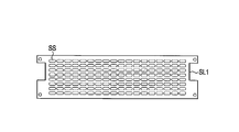
- FIG. 4 is an outline view showing a slit plate having an aperture ratio of 50% according to the present embodiment.
- FIG. 5 is an outline view showing a slit plate with an aperture ratio of 70% according to the present embodiment.
- FIG. 6 is a wind speed distribution diagram showing a wind speed simulation result in a state where there is no slit plate of cooling air flowing through the uninterruptible power supply according to the present embodiment.
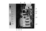
- FIG. 7 is a wind speed distribution diagram showing a wind speed simulation result in a state where there is a slit plate of cooling air flowing through the uninterruptible power supply according to the present embodiment.
- FIG. 1 is a side sectional view showing a configuration of an uninterruptible power supply 1 according to an embodiment of the present invention.
- FIG. 2 is a circuit diagram showing an electric circuit of the uninterruptible power supply 1 according to this embodiment. Note that although the uninterruptible power supply device is described here, any semiconductor device using a semiconductor that requires cooling may be used. Also, the same parts in the drawings are denoted by the same reference numerals, detailed description thereof is omitted, and different parts are mainly described.
- the uninterruptible power supply 1 is a semiconductor device that cools a semiconductor by forced air cooling.
- the uninterruptible power supply 1 is a panel type in which components are housed inside a panel-shaped (cuboid-shaped) housing CH, and is configured to obtain UL (Underwriters Laboratories Inc.) certification.
- the uninterruptible power supply 1 supplies power to the load 23 by AC power supplied from an AC power source 22 such as a commercial power source during normal time (normal time). When the AC power supply 22 fails, power is supplied to the load 23 by DC power supplied from the storage battery 21.
- the uninterruptible power supply 1 includes a chopper circuit (chopper unit) 2, three-phase power conversion circuits (converter units) 3, 4, 5, a cooling fan 7, a diode rectifier DSM, a three-phase input capacitor C1, three An output side capacitor C2, four circuit breakers CB1, CB2P, CB2N, CB3, three reactors L1, L2, L3, and two switches SW1, SW2 are provided.
- the uninterruptible power supply 1 is connected to a storage battery 21, an AC power supply 22, and a load 23, respectively.
- the uninterruptible power supply 1 is connected to an AC power supply 22 by a three-phase three-wire system, and is connected to a load 23 by a three-phase four-wire system.
- the power conversion circuits 3 to 5 are provided corresponding to the U phase, the V phase, and the W phase, respectively.
- the power conversion circuits 3 to 5 are circuits in which the DC sides of the converter circuit CN and the inverter circuit IN are connected by a DC link.
- the AC power input from the AC power supply 22 is input to the power conversion circuits 3 to 5 for each phase through the circuit breaker CB1 and the reactor L2 sequentially.
- the power conversion circuits 3 to 5 convert the input three-phase AC power into DC power and convert it into three-phase AC power supplied to the load 23.
- the power conversion circuits 3 to 5 output the converted three-phase AC power to the load 23 and the cooling fan 7 sequentially through the reactor L3 and the circuit breaker CB3.
- a switch SW2 is provided on the input side of the cooling fan 7.
- Each phase on the input side of the uninterruptible power supply 1 is connected to a neutral point on the output side of the uninterruptible power supply 1 via an input-side capacitor C1.
- Each phase on the output side of the uninterruptible power supply 1 is connected to a neutral point on the output side of the uninterruptible power supply 1 via an output side capacitor C2.
- the storage battery 21 is a battery that stores energy for supplying power in the event of a power failure of the AC power supply 22.
- the DC power output from the storage battery 21 is supplied to the chopper circuit 2 through the two circuit breakers CB2P, CB2N and the reactor L1 provided in the positive and negative electrodes, respectively, in the event of a power failure.
- the chopper circuit 2 adjusts the input DC voltage and supplies DC power to the DC links of the power conversion circuits 3 to 5.
- the diode rectifier DSM converts the three-phase AC power input from the AC power supply 22 via the switch SW ⁇ b> 1 into DC power and outputs the DC power to the chopper circuit 2.
- the chopper circuit 2 operates to charge the storage battery 21 with the DC power input from the DC links of the power conversion circuits 3 to 5 or the diode rectifier DSM.
- FIG. 1 the configuration of the uninterruptible power supply 1 in the panel will be described.
- the arrows in FIG. 1 indicate the flow of cooling air.
- a chopper unit 2 In the panel of the uninterruptible power supply 1, a chopper unit 2, three converter units 3 to 5, a control unit 6, a cooling fan 7, a capacitor unit 8, two circuit breaker units 9 and 10, and three reactors L1, L2 and L3 are implemented. In addition to this, elements and devices constituting the electric circuit shown in FIG. 2 are mounted in the panel of the uninterruptible power supply 1, but they are omitted here.
- the interior of the uninterruptible power supply 1 is divided into two spaces: a space in which most of the components are mounted and a space in which the cooling air passes and the reactors L1 to L3 are mounted.
- the cooling fan 7 for forced air cooling is provided in the space on the back side of the upper surface (ceiling surface) of the housing CH.
- the space on the back side where the cooling fan 7 is provided is wider than the space on the front side.
- the space on the lower side occupying most of the interior of the uninterruptible power supply 1 is wider on the front side than on the back side.
- the front side and the back side are partitioned by a partition plate BD.
- the chopper unit 2 and the converter units 3 to 5 include an electric circuit including a switching element 11 such as an IGBT (insulated gate bipolar transistor).
- the switching element 11 is a semiconductor that generates a large amount of heat and particularly requires cooling.
- the switching element 11 has a thin plate shape.
- the switching element 11 is provided on the upper surface of the cooling fin 12 that cools the switching element 11.
- the switching element 11 and the cooling fin 12 are mounted on the back side of the semiconductor units 2 to 5.
- the semiconductor units 2 to 5 have a structure in which cooling air passes from the front side to the back side.
- the cooling element 12 is cooled by cooling the cooling fins 12 with the cooling air.
- the semiconductor units 2 to 5 are all substantially the same shape, and have a rectangular parallelepiped shape whose height is shorter (lower) than the depth and width.
- the semiconductor units 2 to 5 are provided in a lower space on the front side of the uninterruptible power supply 1.
- the depth of the semiconductor units 2 to 5 is one smaller than the length from the inside of the front surface of the uninterruptible power supply 1 to the partition plate BD. Accordingly, the front surfaces of the semiconductor units 2 to 5 are close (or contact) with the front surface in the panel, and the back surfaces of the semiconductor units 2 to 5 are close (or contact) with the partition plate BD.
- the semiconductor units 2 to 5 are arranged in a vertical direction so as to be stacked in multiple stages, and there is a slight gap between the units 2 to 5.
- Converter unit 5 at the lowest level is installed so as to contact the bottom surface of uninterruptible power supply 1.
- the converter unit 4 is installed on the converter unit 5.
- the converter unit 3 is installed on the converter unit 4.
- the chopper unit 2 at the top of the semiconductor units 2 to 5 is installed on the converter unit 3.
- the capacitor unit 8 is a unit in which the input side capacitor C1 and the output side capacitor C2 shown in FIG. 2 are accommodated.
- the capacitor unit 8 has substantially the same shape as the semiconductor units 2 to 5.
- the capacitor unit 8 is installed on the chopper unit 2.
- the control unit 6 is a unit on which a substrate for controlling the uninterruptible power supply 1 is mounted.
- the control unit 6 is installed on the front side above the capacitor unit 8.
- the circuit breaker unit 9 is a unit in which the two circuit breakers CB2P and CB2N shown in FIG. 2 are accommodated.
- the circuit breaker unit 9 is installed on the back side of the capacitor unit 8.
- the circuit breaker unit 10 is a unit in which the two circuit breakers CB1 and CB3 shown in FIG. 2 are accommodated.
- the circuit breaker unit 10 is provided in a space adjacent to the front side of the space in which the cooling fan 7 is provided.
- the reactors L1 to L3 are installed in a space separated from the partition plate BD on the back side of the space in which the semiconductor units 2 to 5 are mounted.
- Reactors L1 to L3 have a rectangular parallelepiped shape or a cylindrical shape whose longitudinal direction is a vertical direction.
- Reactors L1 to L3 are arranged so as to be stacked in the vertical direction.
- the space in which the reactors L1 to L3 are installed becomes a wind tunnel in which the cooling air discharged from the space in which the semiconductor units 2 to 5 are mounted rises and flows to the cooling fan 7.
- the cooling air inlet Ki is provided in the lower part of the front surface of the uninterruptible power supply 1 at the position where the three semiconductor units (converter units) 3 to 5 are located from the bottom.
- the openings K1 to K4 of the partition plate BD are provided corresponding to the portions located on the back surfaces of the semiconductor units 2 to 5, respectively.
- the cooling air taken in from the front intake port Ki passes through the semiconductor units 2 to 5 so as to cool the cooling fins 12, and passes through the openings K 1 to K 4 of the partition plate BD to the back side of the uninterruptible power supply 1. Discharged into space.
- the cooling air exhausted to the space on the back side flows upward and is exhausted from the cooling fan 7 provided on the upper surface of the uninterruptible power supply 1.
- FIG. 3 is an external view showing an external form in which the slit plates SL1 and SL2 are provided on the partition plate BD according to the present embodiment.
- FIG. 4 is an outline view showing the slit plate SL1 having an aperture ratio of 50%.
- FIG. 5 is an outline view showing the slit plate SL2 having an aperture ratio of 70%.
- the aperture ratio is a ratio in which the aperture ratio of the openings K1 to K4 in a state where no slit plate is provided is 100%.
- the opening K1 at the top and the opening K4 at the top are not provided with a slit plate. That is, the aperture ratio of these openings K1 and K4 is 100%.
- a slit plate SL1 having an aperture ratio of 50% is attached to the second opening K2 from the top.
- a slit plate SL2 having an aperture ratio of 70% is attached to the third opening K3 from the top.
- the aperture ratio of the slit plates SL1 and SL2 is adjusted by the number of slits SS. In addition, you may adjust the aperture ratio of slit board SL1, SL2 with the magnitude
- FIG. 6 is a wind speed distribution diagram showing a wind speed simulation result in a state where there are no slit plates SL1 and SL2 for cooling air flowing through the uninterruptible power supply 1 according to this embodiment.
- FIG. 7 is a wind speed distribution diagram showing a wind speed simulation result in a state where there are slit plates SL1 and SL2 of cooling air flowing through the uninterruptible power supply 1 according to the present embodiment.
- the method to determine the attachment location and aperture ratio of slit board SL1, SL2 is demonstrated.
- a method of determining the slit plates SL1 and SL2 by performing a computer simulation will be described.
- the cooling air velocity may be measured or empirically determined. It may be determined by other methods.
- the wind speed of the cooling air flowing through each of the semiconductor units 2 to 5 varies. Since the cooling fan 7 is attached to the upper part of the uninterruptible power supply 1, the static pressure becomes higher in principle at the top. That is, the wind speed of the cooling air is higher in the upper direction.
- the chopper unit 2 positioned at the top has the intake port Ki at a position slightly below its own height.
- the other converter units 3 to 5 have the intake ports Ki at the respective height positions. Accordingly, the cooling air flowing through the converter units 3 to 5 passes straight from the front side to the back side of each converter unit 3 to 5.
- the cooling air flowing through the chopper unit 2 passes through the chopper unit 2 after being taken into the panel obliquely upward from the lower side. That is, the cooling air flowing through the chopper unit 2 does not flow in a straight line (see FIG. 1). Therefore, the chopper unit 2 is positioned above the converter unit 3, but the cooling air flowing through the chopper unit 2 has a lower wind speed than the cooling air flowing through the converter unit 3.
- the slit plate SL1 having an opening ratio of 50% is attached to the opening K2 located on the back side of the semiconductor unit 3. .
- No slit plate is attached to the openings K1, K2 located in the uppermost semiconductor unit 2 and the lowermost semiconductor unit 5, respectively. That is, these openings K1 and K4 have an opening ratio of 100%. The lower the opening ratio of the openings K1 to K4, the more the cooling air speed passing through the openings K1 to K4 is limited.
- the slit plates SL1 and SL2 that change the aperture ratio are provided in the openings K1 to K4 provided in the partition plate BD, thereby limiting (adjusting) the speed of the cooling air that passes through the openings K1 to K4. )can do.
- the cooling air velocity flowing through each of the semiconductor units 2 to 5 can be made uniform, and the cooling efficiency of the semiconductor units 2 to 5 can be improved.
- a cooling fan is used so that the semiconductor unit 5 having the slowest cooling air is sufficiently cooled without using the slit plates SL1 and SL2. It is possible to select 7. In this case, the cooling air that is faster than necessary flows through the semiconductor unit 3 through which the fastest cooling air flows. That is, the cooling fan 7 consumes excess energy. In contrast, by using the slit plates SL1 and SL2, the speed of the cooling air flowing through each of the semiconductor units 2 to 5 is made uniform, thereby eliminating the semiconductor units 2 to 5 through which the cooling air flows faster than necessary. it can.
- each cooling fin 12 of each of the semiconductor units 2 to 5 without using the slit plates SL1 and SL2 so that the cooling air velocity is made uniform.
- the cooling fins 12 of the converter units 3 to 5 have different shapes, and it is necessary to change the configuration of each converter unit 3 to 5 for each mounting position.
- the converter units 3 to 5 can have a common configuration regardless of the mounting position.
- the size of the space in which the semiconductor units 2 to 5 are mounted (for example, the depth) is made uniform so that the cooling air velocity flowing through the semiconductor units 2 to 5 is uniform. It is possible to change. In this case, there must be enough room in the panel of the uninterruptible power supply 1 to change the size of the space, and there is a possibility that the housing CH will be significantly changed.
- each semiconductor unit 2 to 5 when remodeling in accordance with the specification change of the uninterruptible power supply 1, each semiconductor unit 2 to 5 must be sufficiently cooled even after remodeling.
- the semiconductor units 2 to 5 when the frequency or rated voltage of the uninterruptible power supply 1 is changed, the semiconductor units 2 to 5 are not necessarily cooled as before the remodeling. Therefore, it is necessary to verify the cooling capacity of each of the semiconductor units 2 to 5 in the uninterruptible power supply 1 after modification.
- the uninterruptible power supply 1 after remodeling cannot be cooled sufficiently even by one of the semiconductor units 2 to 5, it is necessary to remodel the uninterruptible power supply 1 again.
- the slit plates SL1 and SL2 are used, the cooling air of each of the semiconductor units 2 to 5 can be easily adjusted, and the cooling capacity of each of the semiconductor units 2 to 5 can be easily changed.
- the structure in the panel or the arrangement of the devices will be changed, or the cooling of the respective semiconductor units 2 to 5
- the shape of the fin 12 must be changed. This increases the remodeling cost as compared with the case where the slit plates SL1 and SL2 are attached.
- the cooling of the semiconductor units 2 to 5 has been mainly described.
- other devices and units such as the control unit 6 and the capacitor unit 8 can be sufficiently configured by using the configuration described in the embodiment. Can be cooled to.
- the configuration of the four-stage stacked semiconductor units 2 to 5 has been described.
- any number of semiconductor units may be used as long as the semiconductor units are stacked in two or more stages.
- the openings K1 to K4 of the partition plate BD are provided corresponding to the semiconductor units 2 to 5, but are not necessarily provided corresponding to the semiconductor units 2 to 5, respectively.
- the cooling capacity of each of the semiconductor units 2 to 5 can be easily adjusted.
- any number of openings may be provided. When there are two openings, a difference in the wind speed of the cooling air passing through the two openings can be reduced by attaching a slit plate to one of the openings.
- the present invention is not limited to the above-described embodiment as it is, and can be embodied by modifying constituent elements without departing from the scope of the invention in the implementation stage.
- various inventions can be formed by appropriately combining a plurality of constituent elements disclosed in the embodiment. For example, some components may be deleted from all the components shown in the embodiment.
- constituent elements over different embodiments may be appropriately combined.
Landscapes
- Engineering & Computer Science (AREA)
- Microelectronics & Electronic Packaging (AREA)
- Physics & Mathematics (AREA)
- Thermal Sciences (AREA)
- Power Engineering (AREA)
- Business, Economics & Management (AREA)
- Emergency Management (AREA)
- Aviation & Aerospace Engineering (AREA)
- Chemical & Material Sciences (AREA)
- Combustion & Propulsion (AREA)
- Mechanical Engineering (AREA)
- General Engineering & Computer Science (AREA)
- Inverter Devices (AREA)
- Cooling Or The Like Of Electrical Apparatus (AREA)
- Cooling Or The Like Of Semiconductors Or Solid State Devices (AREA)
Abstract
無停電電源装置(1)は、盤形状の筐体(CH)と、筐体(CH)の上面から排気し、上面に設けられる冷却ファン(7)と、冷却ファン(7)よりも下にある空間を第1の空間と第2の空間に垂直方向に仕切り、冷却ファン(7)により発生する冷却風が第1の空間から第2の空間に通り抜ける開口部(K1~K4)がある仕切り板(BD)と、冷却風により冷却され、第1の空間に垂直方向に配置される半導体ユニット(2~5)と、仕切り板(BD)の開口部(K1~K4)の少なくとも1つに取り付けられ、冷却風の風速を制限するスリット板(SL1,SL2)とを備える。
Description
本発明は、半導体装置に関する。
一般に、半導体が収納された半導体ユニットで構成された半導体装置が知られている。半導体装置は、半導体を冷却するための冷却構造を備える。
例えば、半導体ユニットを風洞内に引き出し可能に多段積みし、風洞上部に強制風冷用のファンを取り付ける冷却装置において、各半導体ユニットの引き出しに応じて引き出し後の空所を閉鎖するシャッターを設けることが開示されている(特許文献1参照)。
しかしながら、半導体ユニットを垂直方向に配置し、冷却ファンにより上部から冷却風を排気する半導体装置の場合、各段の半導体ユニットを冷却する冷却風の風速に差がでる。このため、各半導体ユニットの冷却効果にバラつきが生じ、半導体装置全体の冷却効率が悪くなる。
本発明の目的は、垂直方向に配置した各半導体ユニットに流れる冷却風の風速の差を減らす半導体装置を提供することにある。
本発明の観点に従った半導体装置は、盤形状の筐体と、前記筐体の上面から排気し、前記上面に設けられる冷却ファンと、前記冷却ファンよりも下にある空間を第1の空間と第2の空間に垂直方向に仕切り、前記冷却ファンにより発生する冷却風が前記第1の空間から前記第2の空間に通り抜ける複数の開口部がある仕切り板と、前記冷却風により冷却され、前記第1の空間に垂直方向に配置される複数の半導体ユニットと、前記仕切り板の前記複数の開口部の少なくとも1つに取り付けられ、前記冷却風の風速を制限するスリット板とを備える。
(実施形態)
図1は、本発明の実施形態に係る無停電電源装置1の構成を示す側方断面図である。図2は、本実施形態に係る無停電電源装置1の電気回路を示す回路図である。なお、ここでは、無停電電源装置について説明するが、冷却を必要とする半導体を用いる半導体装置であれば、どのようなものでもよい。また、図面における同一部分には同一符号を付してその詳しい説明を省略し、異なる部分について主に述べる。
図1は、本発明の実施形態に係る無停電電源装置1の構成を示す側方断面図である。図2は、本実施形態に係る無停電電源装置1の電気回路を示す回路図である。なお、ここでは、無停電電源装置について説明するが、冷却を必要とする半導体を用いる半導体装置であれば、どのようなものでもよい。また、図面における同一部分には同一符号を付してその詳しい説明を省略し、異なる部分について主に述べる。
無停電電源装置1は、強制風冷により半導体を冷却する半導体装置である。無停電電源装置1は、盤形状(直方体形状)の筐体CHの内部に構成部品が収納された盤タイプで、UL(Underwriters Laboratories Inc.)認証が得られる構成である。無停電電源装置1は、通常時(正常時)は、商用電源などの交流電源22から供給される交流電力により、負荷23に電力を供給する。交流電源22が停電すると、蓄電池21から供給される直流電力により、負荷23に電力を供給する。
図2を参照して、無停電電源装置1の回路について説明する。
無停電電源装置1は、チョッパ回路(チョッパユニット)2、三相分の電力変換回路(コンバータユニット)3,4,5、冷却ファン7、ダイオード整流器DSM、三相分の入力側コンデンサC1、三相分の出力側コンデンサC2、4つの遮断器CB1,CB2P,CB2N,CB3、3つのリアクトルL1,L2,L3、及び2つのスイッチSW1,SW2を備える。無停電電源装置1は、蓄電池21、交流電源22及び負荷23とそれぞれ接続されている。無停電電源装置1は、交流電源22と三相三線式で接続され、負荷23と三相四線式で接続されている。
電力変換回路3~5は、それぞれU相、V相及びW相に対応して設けられている。電力変換回路3~5は、コンバータ回路CNとインバータ回路INの直流側同士が直流リンクで接続された回路である。交流電源22から入力された交流電力は、遮断器CB1及びリアクトルL2を順次に介して、相毎に電力変換回路3~5に入力される。電力変換回路3~5は、入力された三相交流電力を直流電力に変換して、負荷23に供給する三相交流電力に変換する。電力変換回路3~5は、変換した三相交流電力をリアクトルL3及び遮断器CB3を順次に介して、負荷23及び冷却ファン7に出力する。冷却ファン7の入力側には、スイッチSW2が設けられている。無停電電源装置1の入力側の各相は、入力側コンデンサC1を介して、無停電電源装置1の出力側の中性点と接続されている。無停電電源装置1の出力側の各相は、出力側コンデンサC2を介して、無停電電源装置1の出力側の中性点と接続されている。
蓄電池21は、交流電源22の停電時に電力を供給するためのエネルギーを蓄える電池である。蓄電池21から出力された直流電力は、停電時に、正極及び負極にそれぞれ設けられた2つの遮断器CB2P,CB2N及びリアクトルL1を順次に介して、チョッパ回路2に供給する。チョッパ回路2は、入力された直流電圧を調整して、電力変換回路3~5のそれぞれの直流リンクに直流電力を供給する。蓄電池21を充電する場合、ダイオード整流器DSMは、スイッチSW1を介して交流電源22から入力される三相交流電力を直流電力に変換して、チョッパ回路2に出力する。チョッパ回路2は、電力変換回路3~5の直流リンク又はダイオード整流器DSMから入力された直流電力により、蓄電池21を充電するように動作する。
図1を参照して、無停電電源装置1の盤内の構成について説明する。図1中の矢印は、冷却風の流れを示している。
無停電電源装置1の盤内には、チョッパユニット2、3つのコンバータユニット3~5、制御ユニット6、冷却ファン7、コンデンサユニット8、2つの遮断器ユニット9,10、及び3つのリアクトルL1,L2,L3が実装されている。なお、この他にも、無停電電源装置1の盤内には、図2に示す電気回路を構成する素子及び機器などが実装されているが、ここでは省略する。
無停電電源装置1の内部は、大半の構成部品が実装された空間と、冷却風が通り抜ける風洞としての役割を持ち、リアクトルL1~L3が実装された空間の2つの空間に分けられる。強制風冷用の冷却ファン7は、筐体CHの上面(天井面)の背面側の空間に設けられている。無停電電源装置1の上部は、冷却ファン7が設けられている背面側の空間が前面側の空間よりも広い。無停電電源装置1の内部の大部分を占める下側の空間は、背面側の空間よりも前面側の空間の方が広い。無停電電源装置1の下側の空間は、前面側と背面側を仕切り板BDで仕切られている。
チョッパユニット2及びコンバータユニット3~5(以下、「半導体ユニット2~5」という。)は、IGBT(insulated gate bipolar transistor)等のスイッチング素子11で構成される電気回路を備える。スイッチング素子11は、発熱量が多く、特に冷却を必要とする半導体である。スイッチング素子11は、薄板形状である。スイッチング素子11は、スイッチング素子11を冷却する冷却フィン12の上面に設けられている。スイッチング素子11及び冷却フィン12は、半導体ユニット2~5の背面側に実装されている。半導体ユニット2~5は、前面側から背面側に冷却風が通り抜ける構造である。冷却フィン12が冷却風により冷却されることで、スイッチング素子11が冷却される。
半導体ユニット2~5は、全てほぼ同形状であり、奥行き及び幅に比べて高さが短い(低い)直方体形状である。半導体ユニット2~5は、無停電電源装置1の前面側で下側の空間に設けられている。半導体ユニット2~5の奥行きは、無停電電源装置1の前面の内側から仕切り板BDまでの長さよりも1回り小さい長さである。従って、半導体ユニット2~5の前面は、盤内の前面に近接(又は接触)し、半導体ユニット2~5の背面は、仕切り板BDに近接(又は接触)している。
半導体ユニット2~5は、多段積みされるように垂直方向に配置されており、各ユニット2~5間には、少し隙間がある。最下段にあるコンバータユニット5は、無停電電源装置1の底面に接触するように設置されている。コンバータユニット4は、コンバータユニット5の上に設置されている。コンバータユニット3は、コンバータユニット4の上に設置されている。半導体ユニット2~5のうち最上段にあるチョッパユニット2は、コンバータユニット3の上に設置されている。
コンデンサユニット8は、図2に示す入力側コンデンサC1及び出力側コンデンサC2が収納されたユニットである。コンデンサユニット8は、半導体ユニット2~5とほぼ同形状である。コンデンサユニット8は、チョッパユニット2の上に設置されている。
制御ユニット6は、無停電電源装置1の制御を行う基板等が実装されたユニットである。制御ユニット6は、コンデンサユニット8の上の前面側に設置されている。
遮断器ユニット9は、図2に示す2つの遮断器CB2P,CB2Nが収納されたユニットである。遮断器ユニット9は、コンデンサユニット8の上の背面側に設置されている。
遮断器ユニット10は、図2に示す2つの遮断器CB1,CB3が収納されたユニットである。遮断器ユニット10は、冷却ファン7が設けられている空間の前面側に隣接する空間に設けられている。
リアクトルL1~L3は、半導体ユニット2~5が実装されている空間の背面側にある仕切り板BDを隔てた空間に設置されている。リアクトルL1~L3は、長手方向が垂直方向の直方体形状又は円柱形状である。リアクトルL1~L3は、垂直方向に積み重なるように配置されている。リアクトルL1~L3が設置されている空間は、半導体ユニット2~5が実装されている空間から排出された冷却風が上昇して、冷却ファン7に流れる風洞となる。
冷却風の吸気口Kiは、無停電電源装置1の前面の下部に、下から3つの半導体ユニット(コンバータユニット)3~5が位置する箇所に設けられている。仕切り板BDの開口部K1~K4は、各半導体ユニット2~5のそれぞれの背面に位置する部分に対応して設けられている。前面の吸気口Kiから取り込まれた冷却風は、各半導体ユニット2~5を冷却フィン12を冷却するように通り抜け、仕切り板BDの各開口部K1~K4から無停電電源装置1の背面側の空間に排出される。背面側の空間に排出された冷却風は、上向きに流れ、無停電電源装置1の上面に設けられた冷却ファン7から排気される。
図3は、本実施形態に係る仕切り板BDにスリット板SL1,SL2が設けられた外形を示す外形図である。図4は、開口率50%のスリット板SL1を示す外形図である。図5は、開口率70%のスリット板SL2を示す外形図である。ここで、開口率は、スリット板が設けられていない状態の開口部K1~K4の開口率を100%とした割合である。
仕切り板BDに設けられた開口部K1~K4のうち1番上にある開口部K1と一番したにある開口部K4にはスリット板が設けられていない。即ち、これらの開口部K1,K4の開口率は、100%である。上から2番目にある開口部K2には、開口率50%のスリット板SL1が取り付けられている。上から3番目にある開口部K3には、開口率70%のスリット板SL2が取り付けられている。スリット板SL1,SL2の開口率は、スリットSSの数により調整される。なお、スリット板SL1,SL2の開口率は、スリットSSの大きさで調整してもよい。
図6は、本実施形態に係る無停電電源装置1に流れる冷却風のスリット板SL1,SL2がない状態の風速シミュレーション結果を表す風速分布図である。図7は、本実施形態に係る無停電電源装置1に流れる冷却風のスリット板SL1,SL2がある状態の風速シミュレーション結果を表す風速分布図である。
図6及び図7を参照して、スリット板SL1,SL2を取り付け箇所及び開口率を決定する方法について説明する。なお、ここでは、コンピュータによるシミュレーションを行うことで、スリット板SL1,SL2を決定する方法について説明するが、シミュレーションではなく、冷却風の風速を実測してもよいし、経験的に決定してもよいし、その他の方法で決定してもよい。
スリット板SL1,SL2がない状態では、各半導体ユニット2~5に流れる冷却風の風速には、バラつきがある。冷却ファン7が無停電電源装置1の上部に取り付けられているため、原則として上の方が静圧は高くなる。即ち、上の方が冷却風の風速が速くなる。但し、1番上に位置するチョッパユニット2は、吸気口Kiが自身の高さよりも少し下の位置にある。これに対し、他のコンバータユニット3~5は、それぞれの高さの位置に吸気口Kiがある。従って、コンバータユニット3~5を流れる冷却風は、それぞれのコンバータユニット3~5の前面側から背面側に一直線上に通り抜ける。これに対し、チョッパユニット2を流れる冷却風は、少し下側から斜め上方向に盤内に取り込まれてからチョッパユニット2を通り抜ける。即ち、チョッパユニット2を流れる冷却風は、一直線上には流れない(図1参照)。従って、チョッパユニット2は、コンバータユニット3よりも上に位置するが、チョッパユニット2を流れる冷却風は、コンバータユニット3を流れる冷却風よりも風速が遅くなる。
図6を参照すると、上から2つ目の半導体ユニット3を流れる冷却風の風速が一番速いため、半導体ユニット3の背面側に位置する開口部K2に開口率50%のスリット板SL1を取り付ける。上から3つ目の半導体ユニット4に位置する開口部K3には、開口部K2に取り付けられたスリット板SL1よりも開口率が高い開口率70%のスリット板SL2を取り付ける。一番上の半導体ユニット2と一番下の半導体ユニット5のそれぞれに位置する開口部K1,K2にはスリット板を取り付けない。即ち、これらの開口部K1,K4は、開口率100%となる。開口部K1~K4の開口率が低いほど、開口部K1~K4を通り抜ける冷却風の風速が制限される。
この状態で、冷却風の風速シミュレーションを行うと、図7に示すようになる。図7に示す風速シミュレーション結果では、各半導体ユニット2~5に流れる冷却風は、ほぼ均一の風速で流れている。従って、スリット板SL1,SL2は、この状態で取り付けることに決定する。もし、各半導体ユニット2~5に流れる冷却風にバラつきがあるようであれば、スリット板SL1,SL2の開口率を変更したり、新たにスリット板を設けたりすることで、各開口部K1~K4の開口率を調整する。この調整を全ての半導体ユニット2~5に流れる冷却風が均一になるまで繰り返す。
本実施形態によれば、仕切り板BDに設けられた開口部K1~K4に開口率を変えるスリット板SL1,SL2を設けることで、開口部K1~K4を通過する冷却風の風速を制限(調整)することができる。これにより、各半導体ユニット2~5に流れる冷却風の風速を均一にして、半導体ユニット2~5の冷却効率を向上させることができる。
例えば、全ての半導体ユニット2~5が十分に冷却されるようにするには、スリット板SL1,SL2を用いずに、最も冷却風が遅い半導体ユニット5が十分に冷却されるように、冷却ファン7を選定することが考えられる。この場合、最も速い冷却風が流れる半導体ユニット3には、必要以上に速い冷却風が流れる。即ち、冷却ファン7は、余分なエネルギーを消費していることになる。これに対して、スリット板SL1,SL2を用いて、各半導体ユニット2~5に流れる冷却風の風速を均一にすることで、必要以上に冷却風が速く流れる半導体ユニット2~5を無くすことができる。従って、前述のスリット板SL1,SL2を用いない場合と比較して、容量の小さい冷却ファン7を選定することができる。これにより、無停電電源装置1の盤内を効率よく冷却し、無停電電源装置1の製造コストを低減することができる。
また、スリット板SL1,SL2を用いずに、各半導体ユニット2~5のそれぞれの冷却フィン12の形状を変えて、各冷却風の風速を均一にすることが考えられる。しかし、この場合は、コンバータユニット3~5の冷却フィン12の形状がそれぞれ異なる形状になり、各コンバータユニット3~5を取り付け位置毎に構成を変える必要がある。これに対し、スリット板SL1,SL2を用いることで、各コンバータユニット3~5の構成を取り付け位置に関係なく共通にすることができる。各コンバータユニット3~5の構成を共通にすることで、無停電電源装置1の生産性が向上し、製造コストを低減することができる。
さらに、スリット板SL1,SL2を用いずに、各半導体ユニット2~5が実装されている空間の寸法(例えば、奥行き)を各半導体ユニット2~5に流れる冷却風の風速が均一になるように変更することが考えられる。この場合、無停電電源装置1の盤内に空間の寸法を変更できるだけの余裕がなければならず、また、筐体CHの大幅な変更を伴う可能性がある。
また、無停電電源装置1の仕様変更に伴って改造をする場合、改造後も各半導体ユニット2~5が十分に冷却されるようにしなければならない。しかし、無停電電源装置1の周波数又は定格電圧が変更になる場合、必ずしも各半導体ユニット2~5が改造前と同様に冷却できるとは限らない。従って、改造後の無停電電源装置1において、各半導体ユニット2~5の冷却能力を検証する必要がある。
もし、改造後の無停電電源装置1において、半導体ユニット2~5のうち1つでも十分に冷却できないものがあった場合、無停電電源装置1を再度改造する必要がある。ここで、スリット板SL1,SL2を用いれば、簡単に、各半導体ユニット2~5の冷却風を個別に調整でき、各半導体ユニット2~5の冷却能力を容易に変更することができる。一方、スリット板SL1,SL2を用いずに、各半導体ユニット2~5の冷却能力を変更する改造をしようとすると、盤内の構造又は機器の配置を変えたり、各半導体ユニット2~5の冷却フィン12の形状を変えたりしなければならない。これは、スリット板SL1,SL2を取り付ける場合と比較して改造コストが高くなる。
さらに、本実施形態では、半導体ユニット2~5の冷却について主に説明したが、制御ユニット6及びコンデンサユニット8などの他の機器及びユニットについても、実施形態で説明した構成にすることで、十分に冷却することができる。
なお、実施形態では、四段積みの半導体ユニット2~5の構成について説明したが、二段以上の多段積みの半導体ユニットであれば、半導体ユニットはいくつでもよい。また、仕切り板BDの開口部K1~K4は、半導体ユニット2~5に対応して設けたが、必ずしもそれぞれ半導体ユニット2~5に対応して設けられていなくてもよい。開口部K1~K4を半導体ユニット2~5に対応して設けることで、各半導体ユニット2~5の冷却能力を調整し易くすることができる。また、2以上の開口部が設けられていれば、いくつの開口部が設けられていてもよい。開口部が2つの場合、一方の開口部にスリット板を取り付けることで、2つの開口部を通り抜ける冷却風の風速の差を減らすことができる。
なお、本発明は上記実施形態そのままに限定されるものではなく、実施段階ではその要旨を逸脱しない範囲で構成要素を変形して具体化できる。また、上記実施形態に開示されている複数の構成要素の適宜な組合せにより、種々の発明を形成できる。例えば、実施形態に示される全構成要素から幾つかの構成要素を削除してもよい。さらに、異なる実施形態にわたる構成要素を適宜組み合わせてもよい。
Claims (5)
- 盤形状の筐体と、
前記筐体の上面から排気し、前記上面に設けられる冷却ファンと、
前記冷却ファンよりも下にある空間を第1の空間と第2の空間に垂直方向に仕切り、前記冷却ファンにより発生する冷却風が前記第1の空間から前記第2の空間に通り抜ける複数の開口部がある仕切り板と、
前記冷却風により冷却され、前記第1の空間に垂直方向に配置される複数の半導体ユニットと、
前記仕切り板の前記複数の開口部の少なくとも1つに取り付けられ、前記冷却風の風速を制限するスリット板と
を備えることを特徴とする半導体装置。 - 前記複数の開口部のうち少なくとも1つは、前記スリット板を取り付けないこと
を特徴とする請求項1に記載の半導体装置。 - 前記スリット板は、複数備え、互いに開口率が異なること
を特徴とする請求項1に記載の半導体装置。 - 前記仕切り板の前記複数の開口部は、前記半導体ユニットに対応して設けられることを特徴とする請求項1に記載の半導体装置。
- 盤形状の筐体の上面から排気する冷却ファンを前記上面に設け、
前記冷却ファンよりも下にある空間を第1の空間と第2の空間に垂直方向に仕切り板により仕切り、
前記仕切り板に、前記冷却ファンにより発生する冷却風が前記第1の空間から前記第2の空間に通り抜ける複数の開口部を設け、
前記仕切り板の前記複数の開口部の少なくとも1つに、前記冷却風の風速を制限するスリット板を取り付けること
を含むことを特徴とする半導体装置の冷却方法。
Priority Applications (2)
| Application Number | Priority Date | Filing Date | Title |
|---|---|---|---|
| CN201580037403.6A CN106664035B (zh) | 2014-07-07 | 2015-04-23 | 半导体装置 |
| US15/371,560 US10347561B2 (en) | 2014-07-07 | 2016-12-07 | Semiconductor apparatus |
Applications Claiming Priority (2)
| Application Number | Priority Date | Filing Date | Title |
|---|---|---|---|
| JP2014139572A JP6285299B2 (ja) | 2014-07-07 | 2014-07-07 | 半導体装置 |
| JP2014-139572 | 2014-07-07 |
Related Child Applications (1)
| Application Number | Title | Priority Date | Filing Date |
|---|---|---|---|
| US15/371,560 Continuation US10347561B2 (en) | 2014-07-07 | 2016-12-07 | Semiconductor apparatus |
Publications (1)
| Publication Number | Publication Date |
|---|---|
| WO2016006300A1 true WO2016006300A1 (ja) | 2016-01-14 |
Family
ID=55063945
Family Applications (1)
| Application Number | Title | Priority Date | Filing Date |
|---|---|---|---|
| PCT/JP2015/062422 Ceased WO2016006300A1 (ja) | 2014-07-07 | 2015-04-23 | 半導体装置 |
Country Status (4)
| Country | Link |
|---|---|
| US (1) | US10347561B2 (ja) |
| JP (1) | JP6285299B2 (ja) |
| CN (1) | CN106664035B (ja) |
| WO (1) | WO2016006300A1 (ja) |
Cited By (1)
| Publication number | Priority date | Publication date | Assignee | Title |
|---|---|---|---|---|
| CN107105597A (zh) * | 2016-02-22 | 2017-08-29 | 富士电机株式会社 | 电源装置 |
Families Citing this family (12)
| Publication number | Priority date | Publication date | Assignee | Title |
|---|---|---|---|---|
| JP2018029443A (ja) * | 2016-08-18 | 2018-02-22 | 東芝三菱電機産業システム株式会社 | 電力変換盤ならびにそれを備えるインバータ装置、無停電電源装置およびパワーコンディショナ |
| CN108733175B (zh) * | 2017-04-17 | 2021-05-07 | 伊姆西Ip控股有限责任公司 | 机架以及用于机架的散热装置 |
| TWI658776B (zh) * | 2017-11-27 | 2019-05-01 | 宏碁股份有限公司 | 電子裝置的散熱系統 |
| US10613595B2 (en) * | 2017-12-28 | 2020-04-07 | Bojan Plavsic | Enclosure for cryptocurrency mining rigs |
| JP7047400B2 (ja) | 2018-01-25 | 2022-04-05 | 富士電機株式会社 | 電力変換装置 |
| JP6970045B2 (ja) * | 2018-03-23 | 2021-11-24 | 株式会社日立インダストリアルプロダクツ | 電力変換装置 |
| US20200335423A1 (en) * | 2018-11-27 | 2020-10-22 | Toshiba Mitsubishi-Electric Industrial Systems Corporation | Semiconductor device |
| JP7389342B2 (ja) * | 2020-01-20 | 2023-11-30 | キョーラク株式会社 | フィラメントの製造方法 |
| JP7115500B2 (ja) * | 2020-03-18 | 2022-08-09 | 富士電機株式会社 | 無停電電源装置および無停電電源装置用制御装置 |
| US11690195B2 (en) * | 2020-09-11 | 2023-06-27 | Abb Schweiz Ag | Power semiconductor cooling system |
| WO2022235631A1 (en) * | 2021-05-04 | 2022-11-10 | Vertiv Corporation | Electronic equipment cabinets with configurable air plenums |
| JP7485855B1 (ja) * | 2022-06-17 | 2024-05-16 | 株式会社Tmeic | 電力変換ユニット |
Citations (3)
| Publication number | Priority date | Publication date | Assignee | Title |
|---|---|---|---|---|
| JP2007295748A (ja) * | 2006-04-26 | 2007-11-08 | Meidensha Corp | 電力変換装置の冷却、防音構造 |
| JP2012009636A (ja) * | 2010-06-25 | 2012-01-12 | Hitachi Ltd | 電力変換装置および電力変換ユニットの冷却方法 |
| JP2015050929A (ja) * | 2013-08-30 | 2015-03-16 | エルエス産電株式会社Lsis Co., Ltd. | インバータ冷却装置 |
Family Cites Families (37)
| Publication number | Priority date | Publication date | Assignee | Title |
|---|---|---|---|---|
| US3649430A (en) * | 1965-10-21 | 1972-03-14 | American Cyanamid Co | Vibration damping laminates |
| JPS52136358A (en) * | 1976-05-10 | 1977-11-15 | Hitachi Ltd | Mounting rack |
| JPS6017938A (ja) * | 1983-07-11 | 1985-01-29 | Hitachi Ltd | 冷却フアン装置 |
| SE456547B (sv) * | 1984-12-07 | 1988-10-10 | Ericsson Telefon Ab L M | Anordning vid kylning av kretskort |
| JPS61267398A (ja) * | 1985-05-22 | 1986-11-26 | 株式会社日立製作所 | 電子装置の冷却構造 |
| JPH04217353A (ja) | 1990-12-18 | 1992-08-07 | Fuji Electric Co Ltd | 多段積み半導体ユニットの冷却装置 |
| US5744213A (en) * | 1995-08-25 | 1998-04-28 | Soltech. Inc. | Enclosure panel with herringbone aperture pattern |
| US5684674A (en) * | 1996-01-16 | 1997-11-04 | Micronics Computers Inc. | Circuit board mounting brackets with convective air flow apertures |
| DE19755944C2 (de) * | 1997-12-16 | 2000-01-13 | Siemens Ag | Anordnung zum Kühlen von elektrischen Baugruppen |
| US6554697B1 (en) * | 1998-12-30 | 2003-04-29 | Engineering Equipment And Services, Inc. | Computer cabinet design |
| US6034870A (en) * | 1999-01-27 | 2000-03-07 | Sun Microsystems, Inc. | Computer system having a highly efficient forced air cooling subsystem |
| US6272012B1 (en) * | 2000-02-03 | 2001-08-07 | Crystal Group Inc. | System and method for cooling compact PCI circuit cards in a computer |
| US6557357B2 (en) * | 2000-02-18 | 2003-05-06 | Toc Technology, Llc | Computer rack heat extraction device |
| DE10136457B4 (de) * | 2001-07-26 | 2005-02-03 | Rittal Gmbh & Co. Kg | Schaltschrank mit einer an der Frontseite angebrachten Schranktür und einer als Schranktür ausgebildeten Rückwand |
| US6735079B2 (en) * | 2002-09-24 | 2004-05-11 | Wistron Corporation | Heat dissipation apparatus |
| JP2005019562A (ja) * | 2003-06-24 | 2005-01-20 | Hitachi Ltd | 電子機器の冷却構造 |
| JP4322637B2 (ja) * | 2003-11-20 | 2009-09-02 | 株式会社日立製作所 | ディスクアレイ装置 |
| US7508663B2 (en) * | 2003-12-29 | 2009-03-24 | Rackable Systems, Inc. | Computer rack cooling system with variable airflow impedance |
| US7652891B2 (en) * | 2004-12-06 | 2010-01-26 | Radisys Corporation | Airflow control system |
| US7286345B2 (en) * | 2005-02-08 | 2007-10-23 | Rackable Systems, Inc. | Rack-mounted air deflector |
| US7215552B2 (en) * | 2005-03-23 | 2007-05-08 | Intel Corporation | Airflow redistribution device |
| JP2007011931A (ja) * | 2005-07-04 | 2007-01-18 | Hitachi Ltd | 記憶制御装置 |
| US7438638B2 (en) * | 2005-10-10 | 2008-10-21 | Chatsworth Products, Inc. | Ratio of open area to closed area in panels for electronic equipment enclosures |
| CN200969073Y (zh) * | 2006-11-13 | 2007-10-31 | 鸿富锦精密工业(深圳)有限公司 | 电脑机箱 |
| US7808792B2 (en) * | 2007-12-18 | 2010-10-05 | Juniper Networks, Inc. | Single fan tray in a midplane architecture |
| US7909902B2 (en) * | 2008-06-12 | 2011-03-22 | International Business Machines Corporation | Modified hexagonal perforated pattern |
| JP5150569B2 (ja) * | 2009-06-30 | 2013-02-20 | 株式会社日立製作所 | 電力変換装置・電力変換ユニットおよび電力変換ユニットの設計方法 |
| CN102480874B (zh) * | 2010-11-23 | 2016-03-23 | 赛恩倍吉科技顾问(深圳)有限公司 | 电子设备的机箱 |
| TW201223390A (en) * | 2010-11-25 | 2012-06-01 | Hon Hai Prec Ind Co Ltd | Server cabinet |
| TW201222205A (en) * | 2010-11-25 | 2012-06-01 | Hon Hai Prec Ind Co Ltd | Server cabinet |
| CN102478927B (zh) * | 2010-11-25 | 2016-09-28 | 鸿富锦精密工业(深圳)有限公司 | 服务器机柜 |
| TW201232223A (en) * | 2011-01-26 | 2012-08-01 | Hon Hai Prec Ind Co Ltd | Electronic equipment |
| JP5712812B2 (ja) * | 2011-06-22 | 2015-05-07 | 富士通株式会社 | コンピュータシステムおよびコンピュータシステムの動作方法 |
| JP5977069B2 (ja) * | 2011-07-08 | 2016-08-24 | 日本電波工業株式会社 | 恒温槽付水晶発振器の温度制御回路 |
| US20130088833A1 (en) * | 2011-10-05 | 2013-04-11 | International Business Machines Corporation | Flexible air duct for equipment cooling |
| JP5648188B2 (ja) * | 2011-12-16 | 2015-01-07 | 株式会社日立産機システム | インバータ制御盤 |
| KR20170014071A (ko) * | 2015-07-28 | 2017-02-08 | 엘에스산전 주식회사 | 냉각 효과를 균일화한 전력전자 기기 외함 |
-
2014
- 2014-07-07 JP JP2014139572A patent/JP6285299B2/ja active Active
-
2015
- 2015-04-23 WO PCT/JP2015/062422 patent/WO2016006300A1/ja not_active Ceased
- 2015-04-23 CN CN201580037403.6A patent/CN106664035B/zh active Active
-
2016
- 2016-12-07 US US15/371,560 patent/US10347561B2/en active Active
Patent Citations (3)
| Publication number | Priority date | Publication date | Assignee | Title |
|---|---|---|---|---|
| JP2007295748A (ja) * | 2006-04-26 | 2007-11-08 | Meidensha Corp | 電力変換装置の冷却、防音構造 |
| JP2012009636A (ja) * | 2010-06-25 | 2012-01-12 | Hitachi Ltd | 電力変換装置および電力変換ユニットの冷却方法 |
| JP2015050929A (ja) * | 2013-08-30 | 2015-03-16 | エルエス産電株式会社Lsis Co., Ltd. | インバータ冷却装置 |
Cited By (1)
| Publication number | Priority date | Publication date | Assignee | Title |
|---|---|---|---|---|
| CN107105597A (zh) * | 2016-02-22 | 2017-08-29 | 富士电机株式会社 | 电源装置 |
Also Published As
| Publication number | Publication date |
|---|---|
| JP2016019324A (ja) | 2016-02-01 |
| CN106664035A (zh) | 2017-05-10 |
| US20170084516A1 (en) | 2017-03-23 |
| US10347561B2 (en) | 2019-07-09 |
| CN106664035B (zh) | 2020-01-03 |
| JP6285299B2 (ja) | 2018-02-28 |
Similar Documents
| Publication | Publication Date | Title |
|---|---|---|
| JP6285299B2 (ja) | 半導体装置 | |
| JP6088157B2 (ja) | 配電盤及びその冷却方法 | |
| CN102299613B (zh) | 电力转换装置 | |
| JP2011160594A (ja) | 電力変換装置 | |
| US10720880B2 (en) | Photovoltaic inverter | |
| JP6296303B2 (ja) | 半導体電力変換装置 | |
| JP6074346B2 (ja) | 配電盤装置 | |
| CN204425196U (zh) | 一种光伏逆变器的功率柜散热装置 | |
| CN105392339A (zh) | 电气柜散热装置及使用该装置的电气柜 | |
| JP2010098865A (ja) | 電力変換装置盤 | |
| US10615715B2 (en) | Power conversion device, cooling structure, power conversion system, and power supply device | |
| JP2000232792A (ja) | 無停電電源装置 | |
| CN204559426U (zh) | 逆变器及其冷却风道结构 | |
| JP6319074B2 (ja) | 電力変換装置 | |
| JPH11220887A (ja) | 電力変換装置 | |
| JP2003259657A (ja) | 電力変換装置 | |
| JP6345578B2 (ja) | パワーコンディショナ | |
| JP2020077818A (ja) | 半導体装置 | |
| WO2020110202A1 (ja) | 半導体装置 | |
| US11259439B2 (en) | Low-voltage switching device having an asymmetrically guided air flow-based cooling system | |
| JP6569888B2 (ja) | 冷却機能付半導体装置 | |
| JP2022076285A (ja) | 無停電電源装置 | |
| WO2023089827A1 (ja) | 無停電電源装置 | |
| CN204538941U (zh) | 储能变流器 | |
| CN105703633A (zh) | 功率转换装置的冷却装置 |
Legal Events
| Date | Code | Title | Description |
|---|---|---|---|
| 121 | Ep: the epo has been informed by wipo that ep was designated in this application |
Ref document number: 15818588 Country of ref document: EP Kind code of ref document: A1 |
|
| NENP | Non-entry into the national phase |
Ref country code: DE |
|
| 122 | Ep: pct application non-entry in european phase |
Ref document number: 15818588 Country of ref document: EP Kind code of ref document: A1 |