WO2016002341A1 - パターン測定方法、及びパターン測定装置 - Google Patents
パターン測定方法、及びパターン測定装置 Download PDFInfo
- Publication number
- WO2016002341A1 WO2016002341A1 PCT/JP2015/063412 JP2015063412W WO2016002341A1 WO 2016002341 A1 WO2016002341 A1 WO 2016002341A1 JP 2015063412 W JP2015063412 W JP 2015063412W WO 2016002341 A1 WO2016002341 A1 WO 2016002341A1
- Authority
- WO
- WIPO (PCT)
- Prior art keywords
- pattern
- fin
- sample
- measurement
- dimension
- Prior art date
- Legal status (The legal status is an assumption and is not a legal conclusion. Google has not performed a legal analysis and makes no representation as to the accuracy of the status listed.)
- Ceased
Links
Images









Classifications
-
- G—PHYSICS
- G01—MEASURING; TESTING
- G01B—MEASURING LENGTH, THICKNESS OR SIMILAR LINEAR DIMENSIONS; MEASURING ANGLES; MEASURING AREAS; MEASURING IRREGULARITIES OF SURFACES OR CONTOURS
- G01B15/00—Measuring arrangements characterised by the use of electromagnetic waves or particle radiation, e.g. by the use of microwaves, X-rays, gamma rays or electrons
-
- G—PHYSICS
- G01—MEASURING; TESTING
- G01B—MEASURING LENGTH, THICKNESS OR SIMILAR LINEAR DIMENSIONS; MEASURING ANGLES; MEASURING AREAS; MEASURING IRREGULARITIES OF SURFACES OR CONTOURS
- G01B15/00—Measuring arrangements characterised by the use of electromagnetic waves or particle radiation, e.g. by the use of microwaves, X-rays, gamma rays or electrons
- G01B15/04—Measuring arrangements characterised by the use of electromagnetic waves or particle radiation, e.g. by the use of microwaves, X-rays, gamma rays or electrons for measuring contours or curvatures
-
- H—ELECTRICITY
- H01—ELECTRIC ELEMENTS
- H01J—ELECTRIC DISCHARGE TUBES OR DISCHARGE LAMPS
- H01J37/00—Discharge tubes with provision for introducing objects or material to be exposed to the discharge, e.g. for the purpose of examination or processing thereof
- H01J37/02—Details
- H01J37/22—Optical, image processing or photographic arrangements associated with the tube
- H01J37/222—Image processing arrangements associated with the tube
-
- H—ELECTRICITY
- H01—ELECTRIC ELEMENTS
- H01J—ELECTRIC DISCHARGE TUBES OR DISCHARGE LAMPS
- H01J37/00—Discharge tubes with provision for introducing objects or material to be exposed to the discharge, e.g. for the purpose of examination or processing thereof
- H01J37/26—Electron or ion microscopes; Electron or ion diffraction tubes
- H01J37/28—Electron or ion microscopes; Electron or ion diffraction tubes with scanning beams
-
- H—ELECTRICITY
- H01—ELECTRIC ELEMENTS
- H01J—ELECTRIC DISCHARGE TUBES OR DISCHARGE LAMPS
- H01J37/00—Discharge tubes with provision for introducing objects or material to be exposed to the discharge, e.g. for the purpose of examination or processing thereof
- H01J37/30—Electron-beam or ion-beam tubes for localised treatment of objects
- H01J37/317—Electron-beam or ion-beam tubes for localised treatment of objects for changing properties of the objects or for applying thin layers thereon, e.g. for ion implantation
-
- H—ELECTRICITY
- H10—SEMICONDUCTOR DEVICES; ELECTRIC SOLID-STATE DEVICES NOT OTHERWISE PROVIDED FOR
- H10P—GENERIC PROCESSES OR APPARATUS FOR THE MANUFACTURE OR TREATMENT OF DEVICES COVERED BY CLASS H10
- H10P74/00—Testing or measuring during manufacture or treatment of wafers, substrates or devices
- H10P74/20—Testing or measuring during manufacture or treatment of wafers, substrates or devices characterised by the properties tested or measured, e.g. structural or electrical properties
- H10P74/203—Structural properties, e.g. testing or measuring thicknesses, line widths, warpage, bond strengths or physical defects
-
- H—ELECTRICITY
- H01—ELECTRIC ELEMENTS
- H01J—ELECTRIC DISCHARGE TUBES OR DISCHARGE LAMPS
- H01J2237/00—Discharge tubes exposing object to beam, e.g. for analysis treatment, etching, imaging
- H01J2237/26—Electron or ion microscopes
- H01J2237/28—Scanning microscopes
- H01J2237/2813—Scanning microscopes characterised by the application
- H01J2237/2817—Pattern inspection
Definitions
- the present invention relates to a pattern measurement method and a pattern measurement device, and more particularly, to a pattern measurement method and a pattern measurement device capable of accurately measuring a pattern having a three-dimensional structure.
- a tapered slope is formed by a focused ion beam (FIB), a surface observation image of the formed slope is obtained using an electron microscope, and an electron beam scanning distance X And calculating the sample thickness t by calculating 2 ⁇ X ⁇ tan ⁇ based on the inclination angle ⁇ of the slope.
- FIB focused ion beam
- a contact hole for conducting between layers of a device having a plurality of hierarchical structures has a diameter of only several tens of nanometers due to miniaturization, but the depth is several thousand due to an increase in the number of layers accompanying an increase in the degree of integration. It extends to nm.
- the Fin line pattern of a FinFET device having a three-dimensional structure has a cross-sectional shape with a width of several tens of nm and a height of several times its height. Since this is a path for the switching current, it is considered that the line width of the line needs to be managed in the height direction with sub-nm accuracy.
- Patent Document 1 if an attempt is made to obtain information in the height direction of the sample based on the scanning distance X of the electron beam and the inclination angle ⁇ of the processing slope, high-precision measurement is performed. I can't. In obtaining the scanning distance, if the starting point (or end point) is not accurately grasped, high-accuracy measurement cannot be expected. However, Patent Document 1 describes a method for accurately obtaining a measurement reference point. There is no.
- a pattern measurement method to be executed comprising: forming a tilted surface in a sample region including a circuit element having a deep hole, a deep groove, or a three-dimensional structure by irradiation with a focused ion beam; and the tilted surface and the sample surface Setting the field of view of the scanning electron microscope to include a boundary between and acquiring an image of the field of view based on a detection signal obtained by scanning an electron beam into the field of view, and the acquired Identifying a first position that is a boundary between the inclined surface and the non-inclined surface using an image, a position of a desired deep hole or deep groove located in the inclined surface, and the depth Or a step of specifying a second position which is a position of a surface of a
- a pattern for executing measurement of a circuit element including a fin-shaped pattern formed on a sample based on a detection signal obtained by a scanning electron microscope as follows.
- a measurement method comprising: forming a slope in a region including the circuit element so that a cross-section of the fin-shaped pattern is exposed on a surface thereof by irradiation with a focused ion beam; an upper end of the fin; and Setting the field of view of the scanning electron microscope so as to include a region below the upper end of the fin, and acquiring an image of the field of view based on a detection signal obtained by scanning the electron beam into the field of view; Using the acquired image, the step of identifying the first position of the upper end of the fin-shaped pattern, and the sample from the upper end of the fin-shaped pattern Based on the step of identifying the second position located on the lower layer side, the dimension in the sample surface direction between the first position and the second position, and the angle of the inclined surface, A pattern measuring method having
- a pattern measuring apparatus for measuring a dimension of a pattern formed on a sample based on a detection signal obtained by a scanning electron microscope, the scanning Based on the signal obtained by the electron microscope, the boundary between the inclined surface and the non-inclined surface formed on the sample is specified, and the sample surface direction between the boundary and the pattern included in the image
- a pattern measuring apparatus includes an arithmetic unit for measuring the dimension of the pattern and measuring the dimension in the height direction of the pattern based on the dimension value and the relative angle between the inclined surface and the sample surface.
- a pattern measuring apparatus for measuring the dimension of a pattern formed on a sample based on a detection signal obtained by a scanning electron microscope below, Based on the signal obtained by the scanning electron microscope, the position of the upper end of the fin-shaped pattern is specified, the position of the silicon oxide layer located on the lower layer side of the fin-shaped pattern is specified, and the fin-shaped pattern The height dimension of the fin-like pattern is determined based on the position of the upper surface of the sample, the dimension of the sample surface direction between the silicon oxide layer and the position, and the angle of the slope formed on the sample. Proposed is a pattern measuring apparatus provided with a desired arithmetic unit.
- the measurement in the depth direction of the pattern can be realized with high accuracy.
- the flowchart which shows the process of obtaining the depth information of a sample.
- the figure which shows the cross-section of FinFET which performed the inclined surface process by the focused ion beam.
- the figure which shows the example of a measurement of the side wall angle of Fin The figure which shows an example of the low magnification image containing an inclination process area
- the embodiments described below relate mainly to a method and apparatus for measuring height using an electron microscope.
- a semiconductor device that is being miniaturized by means other than an electron microscope
- throughput and measurement accuracy decrease, and apparatus management costs increase. Therefore, it is not suitable for mass production.
- a method and apparatus for realizing measurement with good throughput, measurement accuracy, and apparatus management cost without modifying the electron microscope as much as possible will be described.
- a slope that descends obliquely from the sample surface is formed by machining mainly on a region including a portion where a pattern to be measured exists, and a pattern that is exposed on the machining surface and a downward slope Measure the distance to the start position of the sample, and determine the distance between the sample surface in the depth direction (Z direction when the sample surface direction before processing is the XY direction) and the pattern, and the start position of the down slope
- Z direction when the sample surface direction before processing is the XY direction
- the pattern start position of the down slope
- the embodiment described below it becomes possible to measure a change in the dimension of the pattern in the depth direction and a change in the pattern shape accompanying a change in the position in the depth direction without breaking the wafer.
- the pattern cross-sectional shape that appears on the fracture surface becomes smaller as it gets deeper from the wafer surface, is the pattern really thin, or bends in a direction perpendicular to the fracture surface and is centered from the fracture surface? It is impossible to tell whether the sectional shape is apparently small due to the deviation.
- the bending in the depth direction of the pattern is measured as a positional deviation of the pattern exposed in the dug down section, and thus is measured independently of the change in the cross-sectional shape. It becomes possible.
- Pattern measurement that performs pattern measurement based on detection signals obtained by a scanning electron microscope (SEM) as one mode for measuring deep holes, deep grooves, etc. with high precision using high-magnification images
- the method includes the step of irradiating the focused ion beam with a focused ion beam so as to include a pattern or edge to be measured in the processing region and to form a slope in the processing region; and Or at least two regions of the first portion of the pattern and the inclined boundary between the inclined surface and the sample surface, or the second portion of the pattern.
- FOV FOV
- FOV field of view
- a pattern measuring method for calculating a pattern or a dimension between the first portion and the inclined boundary or the second portion is proposed.
- a pattern measuring device for measuring the dimension of a pattern formed on a sample based on a detection signal obtained by a scanning electron microscope, the first measurement image obtained by the scanning electron microscope, A first field of view smaller than the field of view of the first image, a second field of view smaller than the field of view of the first image, a second field of view smaller than the field of view of the first image, the first field of view and the second field of view;
- An input device that sets a length measurement cursor that extracts at least one of a first portion and a second portion that are within at least one of the fields of view and serves as a pattern measurement reference, and a first set by the input device
- the first portion of the pattern is specified in the measurement cursor of the field of view, and is set in the second field of view, between the sample surface and the inclined surface, or in the second field of view.
- Putter in the measuring cursor Second identifying portion we propose a first portion, the boundary, or a pattern measuring apparatus having an arithmetic device for measuring the dimension between
- FIG. 8 is a diagram showing a sample obtained by processing the sample surface using FIB, and in particular, an example in which an inclined surface in a direction crossing the sample surface direction (XY direction) is formed on the sample.
- FIG. 8 the portion where the deep hole pattern is dense is dug.
- an inclined surface is formed that descends from the right to the left in the figure.
- the deep hole pattern is dug in a direction perpendicular to the sample surface, the cross section of the deep hole pattern is exposed on the slope until the slope reaches the depth of the hole bottom of the pattern.
- FIG. 9 is a side view of the sample on which the inclined surface is formed.
- An ion beam is incident from the upper right of the figure, and a processing surface is formed that descends from the right to the left. The place where the sample surface and the processed surface intersect is the excavation start point. From there, a processed surface is formed in which the ion beam goes straight and goes down to the lower left.
- the angle formed by the ion beam and the sample surface, that is, the down angle of the processed surface is 40 °.
- the processed surface is a slope that descends from the surface of the unprocessed sample, the deep hole cross section corresponding to a deeper portion is exposed as the slope is lowered. That is, the cross-sectional shape of the deep hole pattern cut at various depth positions can be seen on the processing surface.
- the depth of the cross section at a position of 4 ⁇ m horizontally from the excavation start point to the left is 3.4 ⁇ m.
- the inclined surface is formed by FIB, and the beam is irradiated from the direction perpendicular to the sample surface (the sample surface in the unprocessed region in FIG. 9) and intersecting the inclined processed surface.
- the signal obtained by the above information on the inclined machining surface is obtained.
- a pattern or cross-sectional shape to be measured is exposed on the inclined processed surface, and the position can be captured by acquiring an image with a CD-SEM.
- the distance between the inclined machining surface and the sample surface boundary (excavation start point) and the pattern or cross-sectional shape to be measured is L
- the depth of the pattern or cross-sectional shape (distance to the sample surface) D is , Can be expressed by Equation 1.
- FIG. 10 is a flowchart showing specific steps for obtaining depth information based on the above arithmetic expression.
- An inclined processing surface as illustrated in FIGS. 8 and 9 is formed in advance using FIB, and processing information (processing position, inclination angle (ion beam irradiation direction, etc.)) is acquired.
- the wafer on which the inclined processing surface is formed is placed on the stage of the SEM, and based on the processing information, the wafer stage is moved so that the FIB processed portion enters the low magnification field of view of the electron microscope (step 1).
- the processed part can be captured in the SEM visual field at a magnification of about 3000 times, for example.
- the brightness and contrast of the FIB processed part are clearly different from those of the surrounding unprocessed part, so the stage position and field movement (beam) are set so that the processed part comes to the center of the SEM visual field by the automatic image identification function. Shift) is automatically performed, and even if the field of view is narrowed by the subsequent high magnification measurement, the processed portion can be captured therein.
- step 2 the part dug diagonally is photographed by connecting a plurality of SEM images (step 2).
- An example is shown in FIG.
- the SEM image has a square shape of 450 nm square. Only the area can be copied.
- the depth of the hole is about 3.4 ⁇ m
- the length in the sample surface direction between the inclined processing surface and the boundary between the sample surface and the portion having a depth of 3.4 ⁇ m is 4 ⁇ m. . Therefore, at least nine SEM images are required to capture the entire region at a magnification of 300,000 times.
- the processing surface which is a downward slope, decreases as the visual field position is shifted, it is necessary to adjust the focus when acquiring the SEM for each region. Therefore, the visual field movement amount from the visual field position including the reference line is recorded, and the focal position is moved downward by the depth D required when the visual field movement amount is set to L in Formula 1. Has a function to modify. In this way, since the focus can be adjusted accurately and quickly, it is possible to increase the accuracy and speed of the measurement value.
- the reference line (excavation start line) in FIG. 11 is specified and a pattern for measuring the depth is selected (step 3).
- a pattern for measuring the depth is selected (step 3).
- the position of the pattern in the cursor is measured by, for example, obtaining the relative position between the cursor and the pattern for each pattern in the cursor. If the contrast between the pattern and the surroundings is clear, the measurement reference position may be extracted by performing binarization processing or the like and obtaining the center of gravity position of the area recognized as the pattern.
- the measurement reference position may be extracted by performing image processing that automatically recognizes the hole bottom.
- the dimension between the identified reference line and the extracted pattern centroid (center) is measured, and the depth D is obtained based on Equation 1 (steps 4 and 5).
- high-precision measurement based on a high-magnification image can be performed even when measuring the depth of a deep hole or the like. If the depth of the deep hole is about 3 ⁇ m, the distance between the position where the bottom of the hole is visible on the FIB processed surface and the reference line is about 4 ⁇ m. If the hole diameter is about 30 nm, the magnification of the SEM image needs to be about 200,000 times to measure the dimension, and the field of view of the SEM image is about 0.7 ⁇ m.
- the reference line is not shown in the SEM image. As described above, it is possible to measure the depth of a deep hole or the like with high accuracy by performing image acquisition using a high-magnification image for each of the inclined boundary and the measurement target.
- the reference line is a line where the reference surface and the oblique digging surface intersect when calculating the depth of the pattern cross section exposed on the FIB oblique digging surface.
- the wafer surface is the reference plane
- the line where FIB oblique digging starts from the wafer surface is the reference line.
- the depth of the hole turn exposed on the oblique digging surface is the depth with respect to the wafer surface.
- this reference line in the SEM image it is necessary to find a line in which the carbon protective film formed on the sample surface starts cutting by FIB processing before starting FIB processing. For this purpose, it is necessary to distinguish the contrast difference between the carbon protective film portion and the obliquely dug portion in the SEM image and to define the boundary line as a reference line.
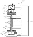
- FIG. 1 is a diagram showing an outline of the SEM 100.
- An electron beam 103 extracted from the electron source 101 by the extraction electrode 102 and accelerated by an accelerating electrode (not shown) is focused by a condenser lens 104 which is a form of a focusing lens, and then is scanned on a sample 109 by a scanning deflector 105.
- a condenser lens 104 which is a form of a focusing lens
- a scanning deflector 105 are scanned one-dimensionally or two-dimensionally.
- the electron beam 103 is decelerated by a negative voltage applied to an electrode built in the sample stage 108, and is focused by the lens action of the objective lens 106 and irradiated onto the sample 109.
- secondary electrons and electrons 110 such as backscattered electrons are emitted from the irradiated portion.
- the emitted electrons 110 are accelerated in the direction of the electron source by an acceleration action based on a negative voltage applied to the sample, and collide with the conversion electrode 112 to generate secondary electrons 111.
- the secondary electrons 111 emitted from the conversion electrode 112 are captured by the detector 113, and the output of the detector 113 changes depending on the amount of captured secondary electrons. In accordance with this output, the brightness of a display device (not shown) changes.
- an image of the scanning region is formed by synchronizing the deflection signal to the scanning deflector 105 and the output of the detector 113.
- the scanning electron microscope illustrated in FIG. 1 includes a deflector (not shown) that moves the scanning region of the electron beam. This deflector is used to form an image of a pattern having the same shape existing at different positions. This deflector is also called an image shift deflector, and enables movement of the field of view of the electron microscope without moving the sample by the sample stage.
- the image shift deflector and the scan deflector may be a common deflector, and the image shift signal and the scan signal may be superimposed and supplied to the deflector.
- the control device 120 controls each component of the scanning electron microscope, and forms a pattern on the sample based on the function of forming an image based on detected electrons and the intensity distribution of detected electrons called a line profile. It has a function to measure the pattern width.
- FIG. 2 is a diagram showing an outline of the FIB apparatus 200.
- This device suppresses the spread of emitted ions, a liquid metal ion source 201 that emits desired ions, an extraction electrode 202 that extracts ions from the liquid metal ion source 201, an aperture 204 that passes only the central portion of the emitted ions 203 downstream.
- a deflector 210 that scans and sweeps the ion beam on the sample surface, an objective lens 211 that focuses the ion beam on the sample surface, a sample stage 212, and a focused ion beam 213 that are emitted when they enter the surface of the sample 206. It comprises a secondary electron detector 214 that captures secondary electrons.
- a control device 215 for controlling each of the above components is provided.
- the control device 215 irradiates a predetermined processing position with the ion beam 213 whose current is adjusted by the diaphragm 208 and scans the ion beam 213 with the deflector 210 to execute drilling processing in a desired region.
- the sample table 212 is provided with a moving mechanism (not shown), and the sample 206 can be moved in the XY direction (when the ion beam irradiation direction is the Z direction) and in the Z direction, and is tilted and rotated. Etc. are configured to be capable of such operations.
- the inclined surface processing as illustrated in FIG. 8 is performed by oblique irradiation of the beam to the sample surface.
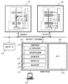
- FIG. 3 is a diagram illustrating an example of a measurement system including the SEM 100 and the FIB apparatus 200.
- the system illustrated in FIG. 3 includes an SEM 100, an FIB device 200, an arithmetic processing device 301, and a design data storage medium 302.
- the arithmetic processing unit 301 supplies control signals including measurement conditions and processing conditions to the SEM 100 and the FIB apparatus 200, and performs processing related to pattern measurement based on the detection signals and measurement results obtained by the SEM 100.
- a processing unit 304, a recipe that is an operation program for determining measurement conditions and processing conditions, and a memory 305 that stores measurement results and the like are incorporated.
- the detection signal obtained by the SEM 100 is supplied to image processing hardware such as a CPU, ASIC, and FPGA built in the arithmetic processing unit 301, and image processing according to the purpose is performed.
- the arithmetic processing unit 304 includes a processing condition setting unit 306 for setting processing conditions of the FIB 200, a measurement condition setting unit 307 for setting measurement conditions by the SEM 100, an area setting unit 308 for setting image acquisition regions and length measurement boxes, and the SEM 100.
- a measurement execution unit 309 that performs measurement based on the obtained detection signal, and a height calculation unit 310 that calculates the height of a pattern or the like based on an arithmetic expression such as Equation 1 stored in advance in the memory 305 or the like. Is built-in. Processing conditions, measurement conditions, and the like can be set by the input device 303, and a recipe for processing and measurement is generated based on the settings.
- the coordinate information and the like of the set processing position are used as measurement conditions of the SEM 100, the information of the incident angle of the ion beam and the like are information for calculating the height (depth) of the height calculation unit 310, and the memory 305. Is remembered.
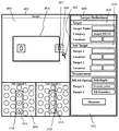
- FIG. 4 is a diagram showing an example of a GUI screen for setting measurement conditions for a processing region by FIB.
- the GUI screen illustrated in FIG. 4 is displayed on the display device of the input device 303, for example, and the arithmetic processing unit 301 selects a recipe that is an operation program for controlling the SEM 100 according to the setting using the GUI screen.
- the program is created and transmitted to the control device 120 that controls the SEM.
- the GUI screen illustrated in FIG. 4 mainly displays an SEM image, and an SEM image display area 402 in which an area on the SEM image can be set by the cursor 401 and the like, and a measurement target setting area for defining a measurement target numerically 403 (Target Definition) is included.
- an area for displaying a target screen (an area for displaying the entire processing area 404 by FIB) 405 indicates the position and size of a high magnification image acquisition area 406 (Sub Target), a pointing device, or the like. It can be set by. Further, in the area 406, a length measurement box 407 for extracting a measurement reference position (measurement start point, measurement end point) can be set. The operation recipe created by setting the area 406 and the length measurement box 407 is used for the control of the SEM 100, and becomes an image acquisition condition displayed in the high magnification image display area 408 (Sub Target).
- the length measurement box is also called a length measurement cursor, and is used for selectively specifying a measurement standard within the area.
- image acquisition conditions and measurement conditions can be set without using a pointing device.
- the measurement target setting area 403 is mainly divided into a setting area 409 for setting target image acquisition conditions and the like, a setting area 410 for setting acquisition conditions for high-magnification images, and a setting area 411 for setting measurement conditions. ing.
- height measurement which is one of the measurement purposes in this embodiment, is selected.
- the setting items in the setting areas 410 and 411 change in accordance with the measurement purpose input.
- the measurement start point and measurement end point are greatly separated, and if the measurement start point and end point are placed within one field of view, high magnification observation cannot be performed.
- Setting items in the setting area 410 are provided so that the acquisition conditions can be set.
- the setting area 410 it is possible to set at least two high-magnification acquisition areas (Sub Tags 1, 2).
- the size of the field of view (FOV size) may be settable.
- processing conditions in the length measurement box 407 can be set according to the measurement purpose.
- the hole depth (Hole Depth) is set as the measurement purpose in the height measurement.
- the processing content for determining the measurement reference changes depending on the measurement start point and the measurement end point. Therefore, it is possible to set the processing content individually. desirable.
- the Sub Target 1 is set to extract the gravity center 413 in the measurement box 412, while the Sub Target 2 is configured to extract the tilt boundary in the measurement box 414. Settings for extracting 415 are made.
- the length measurement box 412 it is necessary to perform pattern recognition and obtain the position of the center of gravity, while in the length measurement box 414, it is necessary to extract an inclined boundary regardless of the position of the pattern.
- Various methods are conceivable as a method for extracting the pattern center of gravity. For example, it is conceivable to extract a contour line of a pattern based on pattern recognition and obtain a center of gravity position based on a distance image of the contour line.
- a method for extracting the inclined boundary a method may be considered in which the boundary between the two is determined in accordance with the luminance difference by using a phenomenon in which the luminance is higher on the inclined surface than on the flat surface due to the edge effect. For example, a waveform profile indicating the luminance change in the X direction of the length measurement box 414 may be acquired and the position where the luminance changes may be specified.
- the presence of a hole pattern may interfere with accurate boundary extraction, so the pattern may be excluded based on pattern recognition, periodic structure extraction processing, etc. Processing such as matching the pixel values with the adjacent background portion may be performed. Note that, unlike a plurality of hole patterns arranged, it is easy to specify an inclined boundary by image processing or the like. Therefore, the inclined boundary may be specified without setting the length measuring cursor 406.
- the position of the Sub target 2 may not be set via the GUI screen, but may be automatically set based on the processing position information supplied to the FIB apparatus 200.
- the brightness change point (boundary between the inclined surface and the sample surface) may be automatically searched in the Subtarget 2 without setting the length measuring box or the like. In order to identify the brightness change point, it is conceivable to obtain a change point by creating a brightness profile in the X direction and differentiating the brightness profile.
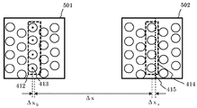
- FIG. 5 is a diagram for explaining a method of measuring the dimension between the gravity center position 413 in the two sub-targets 501 and 502 and the inclined boundary 415.
- images of two sub-targets 501 and 502 are acquired, and the center of gravity position 413 and the position of the inclined boundary 415 are specified in the length measurement boxes 412 and 414 respectively set, and the position, The distance ( ⁇ x b , ⁇ x s ) from the center of the measurement box is obtained.
- the scrolling amount (the amount of deflection of the beam) [Delta] x between the sub target 501 and the sub-target 502, by adding the [Delta] x b and [Delta] x s, exactly the distance between the measurement target pattern and the machining starting point It can be obtained.
- ⁇ x is a value proportional to the amount of signal supplied to the deflector when performing image shift, and is stored in advance in the memory 305 or the like. According to such a method, it becomes possible to accurately measure the distance in the sample surface direction of the measurement target pattern located on the tilt start point and the tilt surface, and as a result, accurate height (depth) measurement is performed. It becomes possible.
- the center position of the sub-target and the measurement box is the same. However, the present invention is not limited to this. Can do. In this case, the deviation between the center positions of the sub-target and the length measurement box is added to the length measurement value.
- FIG. 6 is a diagram illustrating an example in which accurate measurement is possible by acquiring not only the measurement start point and the measurement end point but also the image between them.
- FIG. 6 shows an example in which not only the images of the sub-targets 501 and 502 but also the images of the areas 601 and 602 between them are acquired. If the image acquisition position of the sub-target shifts due to the influence of charging or the like, in the case of a sample in which similar elements are arranged, there is a possibility that an adjacent pattern that is not a measurement target is erroneously recognized as a measurement target is there. Therefore, in this example, the image acquisition regions are set so that the fields of view are superimposed between the two targets at different positions and adjacent to each other. In the example of FIG.
- overlapping regions 603, 604, and 605 are provided, and by performing pattern matching processing (pattern matching) using the overlapping region, it is possible to perform relative alignment between images, and by using intermediate images
- the two targets to be connected are also relatively accurately aligned.
- the measurement start point and the measurement end point that are not within the range in a high-magnification image are measured. Even a measurement object having a high-precision measurement can be performed.
- a value corresponding to L in Formula 1 is obtained by forming a luminance profile across a plurality of images and detecting a change in the profile indicating the pattern gravity center and the tilt boundary. .
- FIG. 18 is a diagram illustrating an example of a low-magnification image 1801 including an inclined processing region.
- a large number of hole patterns 1802 are included in the display area of the low-magnification image 1801.
- a rectangle 1803 indicates a processing region by FIB, and a deep inclined surface processing is performed on the lower side of the drawing.
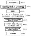
- FIG. 19 is a flowchart illustrating a process of performing automatic measurement on the sample illustrated in FIG.
- a sample that has been processed as illustrated in FIG. 18 is introduced into the SEM (step 1901).
- the stage is moved so that the low-magnification acquisition region matches the field of view of the SEM (step 1902).
- the electron beam is scanned to obtain a low magnification image (step 1903).
- a high-magnification image acquisition FOV for specifying an inclined boundary is set on the low-magnification image or based on the FIB processing position information (step 1904).
- the high-magnification image acquisition FOV is not set at an accurate position due to stage accuracy, process variation, etc., so boundary detection is performed based on the boundary determination algorithm as described above (step 1905) If no boundary is detected, the boundary is detected by setting a field of view in an adjacent region. This process is repeated until a boundary is detected (search around in step 1907). In the example of FIG. 18, when there is no boundary in the first visual field, it is considered that there is a boundary at a different position in the Y direction, so the boundary is detected by moving the visual field in the Y direction.
- an image of a region 1804 located on the inclined processing surface side is acquired with respect to the detected boundary, and a template is created based on the image (steps 1906 and 1908).
- the template is formed by cutting out a part of the low-magnification image.
- a pattern search is executed in the depth direction of the inclined machining surface (step 1909). In making this pattern search performs pattern searching along the depth direction from the region 1804, along with obtaining a distance [Delta] Y 1 of the first matching position 1804, thereafter, it performs template matching for each [Delta] Y 1, matching score May be calculated.
- the position where the matching score is a predetermined value or less is specified while performing the pattern search.
- the area 1806 is a position where the matching score is a predetermined value or less.
- a pattern 1808 included in the region 1806 indicates a resist residue or the like of the hole pattern and corresponds to the bottom of the hole pattern.
- the bottom of the pattern is almost the same height as the inclined machining surface, and compared with other hole patterns that are deep holes, the detection efficiency of electrons emitted from the bottom is high, so it is relative to other hole patterns.
- Bright pattern Since the region 1807 deeper than the region 1806 is deeper than the hole bottom, there is no hole pattern.
- the matching score in the region 1806 decreases. For example, by obtaining a matching score (degree of coincidence) for each ⁇ Y 1 and specifying a portion where the score is equal to or less than a predetermined value, it is possible to specify a pattern indicating the hole bottom.
- the FOV for high magnification image is set so as to include the pattern 1808, and the position of the pattern 1808 is specified by obtaining the pattern center of gravity and the like (steps 1910 and 1911).
- L in Equation 1 can be obtained (step 1912). If a template indicating the hole bottom is prepared in advance, a pattern search using the inclined boundary 1809 as a base point may be performed, and a portion where the matching score is a predetermined value or more may be specified as the pattern bottom. .
- the operation program as described above is stored in the memory 305 of the arithmetic processing unit 301 or a storage medium built in the SEM 100, and the SEM 100 is controlled based on the operation program. Measurement can be performed automatically.
- the above explanation mainly relates to a technique for measuring the depth of a hole pattern, but the above technique can also be applied to the evaluation of the height direction of a pattern having a three-dimensional structure.
- a technique for measuring the depth of a hole pattern for example, in a transistor called FinFET, a large number of structures called Fin are formed in the height direction, and the height of the Fin is an important factor that determines the performance of the circuit. Evaluation item.
- measurement is performed with reference to the surface of the silicon oxide filling between the Fins.
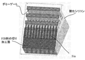
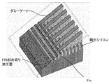
- FIG. 12 is a diagram showing a cross-sectional structure of a FinFET that has been subjected to inclined surface processing by FIB.
- a plurality of dummy gates are arranged in parallel in a direction perpendicular to the direction in which the plurality of Fins are arranged.
- An inclined surface is formed in a direction intersecting a two-dimensional plane including in its plane an imaginary line extending in the longitudinal direction of the Fin and the Fin arrangement direction. Further, the top and bottom of Fin are processed so as to be exposed on the inclined surface.
- the groove between the two fins is filled with silicon oxide, and the tip of the fin protrudes from the silicon oxide layer that is an insulator.
- the FinFET transistor element current flows through the protruding portion. Therefore, in managing the manufacturing process, it is important to measure the width and height of the protruding portion for each Fin.
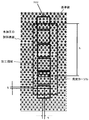
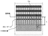
- FIG. 13 is a diagram illustrating an image example (top-down image) in which an inclined surface is imaged with an SEM after an inclined surface is processed on a sample region including a FinFET.
- a virtual line connecting the tops of the Fins 1301 is defined as a reference line 1302.
- This line is the part where the oblique cutting of Fin by FIB has started and is the starting point of the inclined surface of Fin. Further, it is the starting point of the inclined surface and at the same time the upper end position of Fin.
- the cross section of Fin 1301 that penetrates the inside of the dummy gate is visible in the oblique cut section of the dummy gate below the reference line.
- the image illustrated in FIG. 13 includes a dummy gate 1303 and a dummy pattern 1304 partially cut away by the tilting process.
- the layer of silicon oxide 1305 is exposed on the processing surface by the inclination processing.
- the Fin width in the dummy gate is measured together with the Fin height for process management.
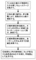
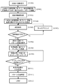
- FIG. 20 is a flowchart illustrating a process of measuring the Fin height, and the measurement system illustrated in FIG. 3 performs measurement according to the flowchart.
- a sample to be measured is introduced into the SEM (step 2001).
- the introduced sample has already been subjected to inclined surface processing by FIB, and the stage (sample stage 108) is moved so that the FOV is positioned on the inclined processed surface (step 2002).
- an image is acquired (step 2003).
- template matching is executed on the acquired image using a template registered in advance (step 2004).
- FIG. 21 is a diagram showing an example of a template.
- the template 2100 includes a part of the fins 1301, a dummy pattern 1304 in which a part of the fins 1301 has been removed by FIB, silicon oxide 1305 exposed on the inclined surface, and a space 2101 between the fins.
- the silicon oxide 1305 exposed on the inclined surface has a relatively high luminance with respect to other portions, and other members are adjacent to each other in the X direction and the Y direction. Therefore, the silicon oxide 1305 and the silicon oxide 1305 are exposed.
- FIG. 22 is a diagram illustrating an example in which ROIs 2201, 2202, and 2203 are set on the upper end of the Fin 1301, the upper surface of the silicon oxide on the right side of the Fin 1301, and the upper surface of the silicon oxide on the left side of the Fin 1301, respectively.
- the ROI has a predetermined positional relationship with the matching position by template matching, and is set on the image based on the position specified by template matching and the positional relationship information.
- the ROI 2201 detects the upper end of the fin 1301, and the ROIs 2202 and 2203 detect the position of the boundary (upper surface of silicon oxide) between the dummy gate 1304 and silicon oxide (step 2006).
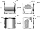
- FIG. 23 is a diagram showing a technique for specifying the tip in the ROI 2201.
- the X-direction luminance distribution acquisition unit 2301 is set for each different position in the Y direction in the ROI 2201, and the tip position of the pattern based on the two-dimensional luminance distribution information 2302 2303 is specified.
- the luminance distribution acquisition unit 2303 may be set at different positions in the X direction, and the tip position 2303 of the pattern may be specified.
- the position may be obtained.
- the boundary position between the two is obtained by acquiring the luminance distribution in the Y direction.
- FIG. 22 shows an example in which fr and fl are obtained by setting ROIs at two left and right positions for one fin.
- the height of the silicon oxide changes alternately or at a specific period. Therefore, in order to quantitatively determine the height of one fin, both the left and right dimensions are used.
- the height of the fin is obtained by substituting L obtained as described above into Equation 1 (step 2008).
- the fin height can be obtained automatically and accurately.
- FIG. 7 is a diagram showing an example of a GUI screen for registering measurement conditions.
- a measurement target setting area 403, a measurement target display area 402, and ROI image display areas 701 and 702 are displayed based on an input using a cursor 401, a keyboard, or the like.
- an operation recipe is created using this GUI screen.
- the arithmetic processing unit 301 reads design data from the design data storage medium 302 and displays it in the measurement target area 402 by designating a pattern or coordinates.
- a three-dimensional image is constructed based on the design data, and the three-dimensional image is displayed in the measurement target region 402. Since the appearance of the inclined machining surface changes according to the inclination angle of the inclined machining surface, the angle of the inclined machining surface (Tilt Angle), the size of the machining site (Site Size), and the position of the machining site (Site Location). ) Can be set. Based on such a condition setting, a three-dimensional image is constructed from the design data. Further, based on this setting, processing conditions by FIB may be set, and an operation recipe of the FIB apparatus 200 may be constructed. Alternatively, a measurement recipe may be automatically set based on the setting of processing conditions on the FIB apparatus side.
- the height of the fin, the measurement start point, or the end point of the oxide film and the fin are set as the measurement purpose.
- a column for setting a specific algorithm for measurement is provided, and one of them is “foot” which is an algorithm suitable for the skirt portion of the fin (the boundary between the oxide film and the dummy gate). “Peak” suitable for specifying the tip is selected.
- foot is an algorithm suitable for the skirt portion of the fin (the boundary between the oxide film and the dummy gate).
- “Peak” suitable for specifying the tip is selected.
- an algorithm suitable for detecting a peak vertex as illustrated in FIG. 23 is set as a measurement condition. Note that by performing processing so that the contact surface of the dummy gate with the oxide film intersects the inclined processing surface, it is possible to specify the boundary line using the luminance difference between the oxide film and the dummy gate.
- Appropriate operating conditions can be easily set by enabling measurement conditions to be set using the GUI screen as described above.
- the Fin width in the dummy gate for various L can be measured. This is data showing how the Fin width changes as it falls from the top of the Fin in the dummy gate, and based on this, the sectional shape of the Fin in the dummy gate is known. be able to.
- a pattern of a three-dimensional structure can be evaluated. Since it takes about one hour to cut and measure, it takes a lot of time and labor to monitor the in-plane distribution in the wafer or chip.
- the cross-sectional shape can be known by FIB oblique cutting that can be done in a few minutes and CD-SEM measurement that can be done in about 10 seconds, thus greatly saving time and labor in the production process. be able to.
- FIG. 14 shows a dummy gate cross-sectional structure obtained by obliquely cutting the FIB.
- FIB is incident in a direction along the longitudinal direction of the dummy gate and in a direction perpendicular to the longitudinal direction of Fin.
- the cross section of the dummy gate is exposed from the top to the bottom.
- the dummy gate is replaced with a conductive metal in a later process, and a voltage is applied to the dummy gate to switch the current flowing through the Fin at the portion where the dummy gate straddles. . Therefore, it is important to measure the width and height of the dummy gate straddling Fin for each dummy gate.
- FIG. 15 shows an example of a dummy gate cross section in which the FIB obliquely cut portion is observed by SEM from above the wafer surface from the top down.
- the dummy gate rides on the silicon oxide and is formed so as to straddle Fin.
- the reference height for measuring the height of the pattern is the surface of the silicon oxide.
- a line whose surface begins to be cut obliquely by FIB is taken as a reference line.
- a cross section of the dummy gate pattern cut obliquely is displayed. The cross section of the dummy gate pattern is exposed on the oblique digging surface.
- the top part of the dummy gate is automatically recognized, and the line width of that part is measured.
- a “height reference line” is set as a base point for pattern height measurement.
- the material is formed at the bottom of the dummy gate. Since the polysilicon changes to silicon oxide, the image contrast also changes abruptly.
- a height reference line is set on the boundary line where the contrast changes.
- the distance between the height reference line and the top portion of the dummy gate in other words, the vertical interval on the SEM image is measured. From that distance, in the actual pattern structure, The height difference in the stacking direction is calculated. The output data of the measurement is only the height difference or a pair of the height difference and the line width dimension measurement value.
- the dummy gate cross section exposed on the oblique cut surface extends downward, but stops where it hits the cross section of the silicon oxide immediately below. This is because the dummy gate is on silicon oxide. Therefore, in order to find the reference line, it suffices to search for a section where the dummy gate cross section cuts downward.
- FIG. 16 shows an example of measurement of bending in deep hole machining.
- the figure is a schematic diagram of a top-down image of the deep hole machining region, and the FIB oblique digging surface that is descending from the top to the bottom of the figure is visible.
- the FIB oblique digging surface that is descending from the top to the bottom of the figure is visible.
- the entrance of the deep hole is visible. If the deep hole is dug perpendicular to the sample surface, the entrance of the deep hole and the cross-sectional shape of the processing area appear side by side on a virtual straight line in the horizontal or vertical direction in the figure.
- the measurement target pattern is shifted from the virtual straight line by B in the right direction. Further, it is separated by a distance L from the reference line. Therefore, it can be seen that the measurement target pattern is shifted from the wafer surface by B in the right direction in the drawing at a depth L ⁇ tan ⁇ . That is, it can be seen that the measurement target pattern is bent rightward at a deep portion.
- a search using a template as illustrated in FIG. 18 is performed in the Y direction, and the degree of coincidence becomes a predetermined value or less. It is conceivable to use (the place where the score is lowered due to the pattern shift) as a reference for depth measurement. Further, another algorithm for specifying the inflection point of the array of patterns arranged linearly may be applied.
- Fig. 17 shows an example of Fin side wall angle measurement.
- ⁇ be the angle formed by the side wall of a certain Fin pattern with the horizontal direction of the screen.
- the distance between the position on the screen where the angle is measured and the reference line is L.
- the side wall angle ⁇ between the actual Fin pattern and the horizontal surface of the wafer surface is calculated by the following equation.
- planar unevenness of the Fin sidewall adversely affects the electrical characteristics of the FinFET device. Therefore, in the production process, it is important to measure the planar unevenness of the side wall and manage the process.
- the sidewall surface has a substantially horizontal angle with respect to the incident direction of the electron beam of the SEM image, the unevenness on the sidewall surface is hardly visible in the SEM image.
- the top-down SEM image of the surface dug obliquely by FIB can capture irregularities relatively well. This is because, if a slope that descends in the longitudinal direction of the Fin line is formed by oblique digging of the FIB, the top-down SEM image of the slope has the side wall of the Fin pattern substantially perpendicular to the side wall surface. The cross-sectional shape cut out in a plane is shown. There is a line edge roughness (LER: Line Edge) on the Fin side wall. It is observed that Roughness) changes with respect to the height direction of Fin. This makes it possible to more clearly observe the LER on the side wall as compared with the conventional method of measuring with a Fin pattern top-down SEM image without oblique digging.
- LER Line Edge
- the obliquely dug surface has a side wall cut out and an approximately 90 ° edge appears in that portion. Such an edge appears clearly in the SEM image, but such an edge does not exist when not digging diagonally.
- a side wall LER that changes in the Fin height direction is shown. Since this is a LER including both the LER in the longitudinal direction and the LER in the height direction of the side wall, it can be applied to process management as an index value indicating the unevenness of the side wall.
- the SEM 100 and the FIB device 200 are independent devices, but can be connected by a network by LAN communication.
- coordinate information on a wafer processed in the FIB apparatus is sent to the SEM 100 via a network.
- a top-down image acquired by the SEM mounted on the FIB may be sent to the SEM 100 together with coordinate data. If the SEM can be controlled using the coordinate data acquired in advance, it is possible to automatically position the measurement target position at the visual field position of the SEM.
- ⁇ Since coordinate data is sent from FIB, search for the processed place around that place. If an SEM image of the processed part has been sent, it is possible to automatically search for a place similar to the image in the wafer surface.
- the data measured by the SEM apparatus may be sent to an external storage medium through LAN communication.
- OTL overlay
- a via-in trench structure in which a via hole is formed at the bottom of a trench, it is important to make a hole so that the center of the hole is located on the center line of the trench.
- Overlay measurement to be measured is necessary for process management.
- the deeper the groove the more difficult the secondary electrons generated at the bottom reach the detector, so that the image of the hole at the bottom of the groove becomes relatively unclear, and OVL measurement between the center line of the groove and the center of the hole is performed. The length tends to be relatively low in accuracy.
- the OVL measurement accuracy can be improved.
- the depth of the slope becomes deeper than the groove bottom, the cross section of the hole vacated in the groove bottom will be visible on the slope, so by measuring these, the shape change in the depth direction of the hole and the hole It is possible to measure quantitatively whether the wafer is vacant in a direction perpendicular to the wafer surface.
- Such OVL measurement can be applied to various other things such as OVL measurement of a resist pattern on the wafer surface and a pattern formed inside the wafer.
- OVL measurement can be performed with higher accuracy than measurement using a general SEM. This is because the measurement using a general SEM cannot sufficiently capture the secondary electrons emitted from the hole bottom, and the image quality of the pattern is extremely lowered.
- the pattern in the wafer and the wafer surface are paired to form a capacitor locally, and the charge trapped in the capacitance May be locally charged. Since the orbit of electrons emitted from the sample changes due to charging, the observed image also becomes an image reflecting the charging. However, since this charged image is not the pattern in the wafer itself, and the outline of the charged region is not clear, there is a possibility that the OVL measurement accuracy is reduced. On the other hand, by performing measurements based on inclined surface processing, the actual pattern appearing on the surface of the slope can be measured, and secondary electrons from it can be measured directly, resulting in a clearer pattern outline and OVL measurement accuracy. Can be improved.
- Wafers dug with FIB should be returned to the production line without being discarded, and Yield should not fall. This is because the part processed by FIB is difficult to reproduce in a later process, but the other parts that are not damaged function as a device after the subsequent process. Actually, for example, a shot or a chip including a part processed by FIB is recorded, and only the shot is discarded after a subsequent dicing process.
- the carbon protective film covers the device pattern, Ga metal contamination occurs due to the Ga ion beam, or foreign matter contamination due to particles scattered from the portion occurs. However, such a region is about a few microns in radius centered on the FIB processed part, so if you discard that part for every shot that is about 10 mm or more in size, other shots Can be obtained later as good products without being affected by such effects.
- a normal FIB processing apparatus has a gimbal mechanism in which a stage on which a wafer is placed can be tilted in various directions so that the incident direction of the FIB on the wafer surface can be changed.
- a stage having a relatively simple structure that can hold the wafer without being tilted horizontally without using such a gimbal mechanism is used, and the FIB column has an elevation angle of, for example, 40 ° with respect to the surface of the wafer. Fix at an angle. In this way, the generation of foreign matter from the gimbal mechanism can be eliminated, so that foreign matter contamination of the wafer can be suppressed and the wafer can be returned to the production process.
- the elevation angle with respect to the wafer is 40 ° or less, the column comes into contact with the wafer, so the elevation angle is made as small as possible. This is because the smaller the elevation angle, the more cross-sectional shapes can be captured on the FIB processed surface. This is because changes in the cross-sectional shape in the depth direction can be measured more finely. In other words, it is not necessary to change the elevation angle in various ways by the gimbal mechanism, and if the wafer stage and FIB column are fixed so as to make the elevation angle as small as possible, the pattern in the depth direction by oblique digging is used. Can be measured more finely and wafers with almost no foreign matter contamination can be returned to the production process, making it possible to measure without almost reducing the yield, and the structure of the equipment is simple, so the equipment investment is reduced by reducing the equipment price. Can be reduced.
- a mechanism for rotating the wafer with the normal line of the wafer surface passing through the center point of the wafer as the rotation axis is necessary.
- the Fin line and the Gate line are formed so as to be orthogonal to each other, and in order to measure the shape change in both depth (height) directions, oblique digging by FIB is performed in two directions. It is necessary to do from.
- a mechanism for rotating the wafer stage is built in, particles are generated from the wafer stage, causing foreign matter contamination.
- a mechanism for rotating the wafer to an arbitrary angle is provided.
- the wafer is rotated with the orientation flat of the wafer as a mark so that the longitudinal direction of the Fin line or the Gate line is parallel to the FIB beam, the wafer is placed on the wafer stage, and oblique digging by FIB is started. good.
Landscapes
- Physics & Mathematics (AREA)
- Chemical & Material Sciences (AREA)
- Analytical Chemistry (AREA)
- Electromagnetism (AREA)
- General Physics & Mathematics (AREA)
- Engineering & Computer Science (AREA)
- Computer Vision & Pattern Recognition (AREA)
- Length-Measuring Devices Using Wave Or Particle Radiation (AREA)
- Testing Or Measuring Of Semiconductors Or The Like (AREA)
Abstract
Description
、深溝、或いは立体構造を有する回路素子を構成するパターンの高さ方向の寸法を求めるステップを有するパターン測定方法を提案する。
図10は、上記演算式に基づいて、深さ情報を得る具体的な工程を示すフローチャートである。予め、FIBを用いて図8、9に例示したような傾斜加工面を形成しておき、その加工情報(加工位置、傾斜角度(イオンビームの照射方向等))を取得しておく。傾斜加工面が形成されたウエハをSEMのステージに配置し、加工情報に基づいて、FIB加工された部分が電子顕微鏡の低い倍率視野に入るように、ウエハステージを動かす(ステップ1)。上述のように、FIB加工された部分の座標データ(加工位置情報)は、FIB加工装置から送られているため、例えば3000倍程度の倍率で、加工部分をSEM視野内にとらえることができる。その際、FIB加工部分の明るさやコントラストは、明らかに周囲の未加工部分とは異なるので、画像の自動識別機能により、その加工部分がSEM視野の中心に来るようにステージ位置や視野移動(ビームシフト)を自動的に行い、このあとの高倍率測定で視野が狭くなってもその中に加工部分をとらえることができるようになる。
なく、画像取得条件や測定条件の設定が可能となっている。測定対象設定領域403は主に、ターゲットの画像取得条件等を設定するための設定領域409、高倍率画像の取得条件を設定する設定領域410、測定条件を設定する設定領域411の3つに分かれている。設定領域409の測定目的(Category)を入力するウィンドウには、本実施例における測定目的の1つである高さ測定(Height Measurement)が選択されている。この測定目的の入力に応じて、設定領域410、411における設定項目が変化する。先述したように、高さ測定の場合、測定始点と測定終点が大きく離間し、1つの視野内に測定始点と終点を収めようとすると、高倍率観察ができなくなるため、複数の高倍率画像の取得条件が設定できるように、設定領域410の設定項目が設けられる。設定領域410では少なくとも2つの高倍率取得領域(Sub Taget 1、2)の設定を可能としている。また、図示はしないが、視野(Field Of Veiw)の大きさ(FOV size)の大きさを設定可能とするようにしても良い。設定領域411では測定目的に応じた測長ボックス407内の処理条件の設定が可能となっている。図4に例示するGUI画面では、高さ測定の中でもホールの深さ(Hole Depth)が測定目的として設定されている。
パターン重心を抽出する手法として、種々の方法が考えられるが、例えばパターン認識に基づいて、パターンの輪郭線を抽出し、当該輪郭線の距離画像に基づいて、重心位置を求めることが考えられる。また、傾斜境界を抽出する手法としては、エッジ効果により、平坦面より傾斜面の方が輝度が大きくなる現象を利用して、輝度差に応じて両者の境界を決定する手法が考えられる。例えば、測長ボックス414のX方向の輝度変化を示す波形プロファイルを取得し、輝度が変化する位置を特定するようにしても良い。また、傾斜境界を抽出する場合、ホールパターンの存在が正確な境界抽出の妨げになる可能性もあるため、パターン認識や周期性のある構造物の抽出処理等に基づいて、パターンを除外、或いは隣接する背景部と画素値を一致させる等の処理等を行うようにしても良い。なお、複数配列されているホールパターンと異なり、画像処理等によって、傾斜境界の特定は容易であるため、測長カーソル406の設定なしに、傾斜境界を特定するようにしても良い。
リングするためには多大な時間と労力が必要となる。一方、上述のような手法によれば、数分でできるFIB斜め切り加工と、10秒程度でできるCD-SEM計測で断面形状を知ることができるので、生産プロセスにおける時間と労力を大幅に節約することができる。
積層方向の高低差」を算出する。計測の出力データは、その高低差のみ、または高低差と線幅寸法計測値とをペアにしたものである。
これは、斜断面の傾きθにより、斜断面に露出している側壁角度が見かけ上変わることを考慮したものである。
Roughness)がFinの高さ方向に対して変化しているのが、観測されている。これは、従来の、斜め掘りをしていないFinパターンのトップダウンSEM像で測定する方式に比べて、側壁のLERをより明瞭に観測することが可能である。なぜなら、斜め掘りされた表面は側壁を切り取っていて、その部分はほぼ90°のエッジが表れているからである。このようなエッジはSEM像においては明瞭に写るが、斜め掘りをしない場合には、このようなエッジは存在しない。さらに、Finラインパターンの長手方向に進むにつれて、Finの高さ方向に変化している側壁LERが写っている。これは、長手方向のLERと、側壁の高さ方向のLERとの両方を含んだLERであるから、これを側壁の凹凸を示す指標値として、プロセス管理に応用することができる。
半径数ミクロン程度の大きさであるから、大きさが約10ミリ以上もあるショットごとその部分を廃棄してしまえば、他のショットはそのような影響を受けずに、後に良品として得ることが可能である。
101 電子源
102 引出電極
103 電子ビーム
104 コンデンサレンズ
105 走査偏向器
106 対物レンズ
107 真空試料室
108 試料台
109 試料
110 電子
111 二次電子
112 変換電極
113 検出器
120 制御装置
200 FIB装置
201 液体金属イオン源
202 引き出し電極
203 放出イオン
204 アパーチャ
205 集束レンズ
206 試料
207 ブランカ
208 絞り
209 アライナ
210 偏向器
211 対物レンズ
212 試料台
214 二次電子検出器
215 制御装置
301 演算処理装置
302 設計データ記憶媒体
Claims (15)
- 走査電子顕微鏡によって得られた検出信号に基づいて、試料に形成された深穴、深溝、或いは立体構造を有する回路素子を構成するパターンの測定を実行するパターン測定方法であって、
集束イオンビームの照射によって、前記深穴、深溝、或いは立体構造を有する回路素子を含む試料領域に傾斜面を形成するステップと、
前記傾斜面と前記試料表面との間の境界を含むように、前記走査電子顕微鏡の視野を設定し、当該視野への電子ビームの走査によって得られる検出信号に基づいて、前記視野の画像を取得するステップと、
当該取得された画像を用いて、前記傾斜面と非傾斜面の境界となる第1の位置を特定するステップと、
前記傾斜面内に位置する所望の深穴または深溝の位置、前記深穴または深溝の底、或いは前記立体構造を有するパターンに交差する層の表面の位置である第2の位置を特定するステップと、
前記第1の位置と前記第2の位置との間の前記試料表面方向の寸法と、前記斜面の角度に基づいて、前記深穴、深溝、或いは立体構造を有する回路素子を構成するパターンの高さ方向の寸法を求めるステップを有することを特徴とするパターン測定方法。 - 請求項1において、
前記深穴は、半導体ウェハに形成されたコンタクトホールであることを特徴とするパターン測定方法。 - 請求項2において、
前記第2の位置は、前記コンタクトホールの底を示すパターン部位、前記コンタクトホールの重心位置、或いはコンタクトホールの当該コンタクトホールの深さ方向に対し直交する方向の位置が変位した位置であることを特徴とするパターン測定方法。 - 走査電子顕微鏡によって得られた検出信号に基づいて、試料に形成されたフィン状のパターンを含む回路素子の測定を実行するパターン測定方法であって、
集束イオンビームの照射によって、前記フィン状のパターンの断面がその表面に露出するように、前記回路素子を含む領域に斜面を形成するステップと、
前記フィンの上端、及び当該フィンの上端より下層側の領域を含むように、前記走査電子顕微鏡の視野を設定し、当該視野への電子ビームの走査によって得られる検出信号に基づいて、前記視野の画像を取得するステップと、
当該取得された画像を用いて、前記フィン状のパターンの上端の第1の位置を特定するステップと、
当該フィン状のパターン上端より試料の下層側に位置する第2の位置を特定するステップと、
前記第1の位置と前記第2の位置との間の前記試料表面方向の寸法と、前記斜面の角度に基づいて、前記フィン状のパターンの高さ方向の寸法測定を実行するステップを有することを特徴とするパターン測定方法。 - 請求項4において、
前記回路素子はFinFETであることを特徴とするパターン測定方法。 - 請求項5において、
前記第2の位置について、前記フィンの幅の寸法を測定することを特徴とするパターン測定方法。 - 請求項6において、
前記第2の位置のフィンの側壁の角度を測定することを特徴とするパターン測定方法。 - 走査電子顕微鏡によって得られた検出信号に基づいて、試料上に形成されたパターンの寸法を測定するパターン測定装置において、
前記走査電子顕微鏡によって得られた信号に基づいて、前記試料に形成された傾斜面と非傾斜面との間の境界を特定し、当該境界と前記画像内に含まれるパターンとの間の前記試料表面方向の寸法を測定し、当該寸法値と、前記傾斜面と試料表面との間の相対角に基づいて、前記パターンの高さ方向の寸法を測定する演算装置を備えたことを特徴とするパターン測定装置。 - 請求項8において、
前記演算装置は、少なくとも2つの視野位置から取得された画像に基づいて、前記傾斜面と非傾斜面との間の境界、及び前記パターンの位置を演算することを特徴とするパターン測定装置。 - 請求項8において、
前記演算装置は、前記パターンの重心を特定し、当該重心と前記境界との間の寸法を測定することを特徴とするパターン測定装置。 - 請求項8において、
前記演算装置は、前記パターンの底を示す位置を特定し、当該パターンの底を示す位置と前記境界との間の寸法を測定することを特徴とするパターン測定装置。 - 請求項8において、
前記演算装置は、前記パターンが、前記パターンの深さ方向に対して直交する方向に変位する位置を特定し、当該位置と前記境界との間の寸法を測定することを特徴とするパターン測定装置。 - 走査電子顕微鏡によって得られた検出信号に基づいて、試料上に形成されたパターンの寸法を測定するパターン測定装置において、
前記走査電子顕微鏡によって得られた信号に基づいて、フィン状のパターンの上端の位置を特定し、当該フィン状のパターンより下層側に位置する酸化シリコン層の位置を特定し、前記フィン状のパターンの上端の位置と、前記酸化シリコン層と位置との間の前記試料表面方向の寸法と、前記試料上に形成された斜面の角度に基づいて、前記フィン状のパターンの高さ方向の寸法を求める演算装置を備えたことを特徴とするパターン測定装置。 - 請求項13において、
前記演算装置は、前記酸化シリコンとフィンが含まれるテンプレートを用いたテンプレートマッチングに基づいて、前記フィン状のパターンの上端の位置、及び酸化シリコン層の位置を特定することを特徴とするパターン測定装置。 - 請求項14において、
前記演算装置は、フィン状のパターンの上端位置と、当該フィン状のパターンの裾部分の位置の特定に基づいて、前記フィン状のパターンの高さ方向の寸法を求めることを特徴とするパターン測定装置。
Priority Applications (3)
| Application Number | Priority Date | Filing Date | Title |
|---|---|---|---|
| KR1020167036187A KR101957007B1 (ko) | 2014-06-30 | 2015-05-11 | 패턴 측정 방법 및 패턴 측정 장치 |
| JP2016531172A JP6427571B2 (ja) | 2014-06-30 | 2015-05-11 | パターン測定方法、及びパターン測定装置 |
| US15/322,338 US10184790B2 (en) | 2014-06-30 | 2015-05-11 | Pattern measurement method and pattern measurement device |
Applications Claiming Priority (2)
| Application Number | Priority Date | Filing Date | Title |
|---|---|---|---|
| JP2014-133502 | 2014-06-30 | ||
| JP2014133502 | 2014-06-30 |
Publications (1)
| Publication Number | Publication Date |
|---|---|
| WO2016002341A1 true WO2016002341A1 (ja) | 2016-01-07 |
Family
ID=55018897
Family Applications (1)
| Application Number | Title | Priority Date | Filing Date |
|---|---|---|---|
| PCT/JP2015/063412 Ceased WO2016002341A1 (ja) | 2014-06-30 | 2015-05-11 | パターン測定方法、及びパターン測定装置 |
Country Status (5)
| Country | Link |
|---|---|
| US (1) | US10184790B2 (ja) |
| JP (1) | JP6427571B2 (ja) |
| KR (1) | KR101957007B1 (ja) |
| TW (1) | TWI586934B (ja) |
| WO (1) | WO2016002341A1 (ja) |
Cited By (14)
| Publication number | Priority date | Publication date | Assignee | Title |
|---|---|---|---|---|
| WO2009154132A1 (ja) | 2008-06-19 | 2009-12-23 | 萬有製薬株式会社 | スピロジアミン-ジアリールケトオキシム誘導体 |
| WO2018042600A1 (ja) * | 2016-09-01 | 2018-03-08 | 株式会社日立ハイテクノロジーズ | 画像解析装置および荷電粒子線装置 |
| CN109841534A (zh) * | 2017-11-28 | 2019-06-04 | 日本株式会社日立高新技术科学 | 截面加工观察方法、带电粒子束装置 |
| US20190170509A1 (en) * | 2016-07-28 | 2019-06-06 | Hitachi High-Technologies Corporation | Pattern Measurement Method and Pattern Measurement Device |
| KR20200096619A (ko) | 2018-02-28 | 2020-08-12 | 주식회사 히타치하이테크 | 이온 밀링 장치 및 이온 밀링 장치의 이온원 조정 방법 |
| JPWO2022064707A1 (ja) * | 2020-09-28 | 2022-03-31 | ||
| JPWO2022158107A1 (ja) * | 2021-01-21 | 2022-07-28 | ||
| JP2022535601A (ja) * | 2019-06-07 | 2022-08-09 | カール・ツァイス・エスエムティー・ゲーエムベーハー | 改善された3dボリューム像再構成精度を有する断面イメージング |
| JP2023501243A (ja) * | 2019-10-30 | 2023-01-18 | カール・ツァイス・エスエムティー・ゲーエムベーハー | 集積半導体サンプルにおける3d構造間の接触領域のサイズ決定 |
| TWI810251B (zh) * | 2018-03-07 | 2023-08-01 | 日商日立高新技術科學股份有限公司 | 截面加工觀察裝置、截面加工觀察方法、程式及形狀測定方法 |
| JP2023547856A (ja) * | 2020-10-23 | 2023-11-14 | アプライド マテリアルズ イスラエル リミテッド | Fib斜め切削を使用した孔の傾斜角の測定 |
| KR20240048549A (ko) | 2021-09-30 | 2024-04-15 | 주식회사 히타치하이테크 | 해석 시스템 |
| TWI862821B (zh) * | 2020-04-17 | 2024-11-21 | 日商東實先進股份有限公司 | 圖形匹配方法 |
| KR20250002493A (ko) | 2022-06-13 | 2025-01-07 | 주식회사 히타치하이테크 | 이온 밀링 장치, 홀더 및 단면 밀링 처리 방법 |
Families Citing this family (22)
| Publication number | Priority date | Publication date | Assignee | Title |
|---|---|---|---|---|
| TWI581304B (zh) * | 2011-07-27 | 2017-05-01 | 日立全球先端科技股份有限公司 | Plasma etching apparatus and dry etching method |
| WO2016016957A1 (ja) * | 2014-07-30 | 2016-02-04 | 株式会社 日立ハイテクノロジーズ | パターン高さ測定装置、及び荷電粒子線装置 |
| CN108700412B (zh) * | 2016-04-13 | 2020-05-08 | 株式会社日立高新技术 | 图案测量装置和图案测量方法 |
| US10115621B2 (en) | 2016-05-13 | 2018-10-30 | Globalfoundries Inc. | Method for in-die overlay control using FEOL dummy fill layer |
| JP6942555B2 (ja) * | 2017-08-03 | 2021-09-29 | 東京エレクトロン株式会社 | 基板処理方法、コンピュータ記憶媒体及び基板処理システム |
| JP6541161B2 (ja) * | 2017-11-17 | 2019-07-10 | 株式会社日立ハイテクサイエンス | 荷電粒子ビーム装置 |
| US10510623B2 (en) | 2017-12-27 | 2019-12-17 | Taiwan Semiconductor Manufacturing Co., Ltd. | Overlay error and process window metrology |
| KR102538024B1 (ko) * | 2018-01-19 | 2023-05-30 | 삼성전자주식회사 | 웨이퍼 측정 설비, 웨이퍼 측정 시스템 및 이를 이용한 반도체 장치의 제조 방법 |
| JP2019185972A (ja) * | 2018-04-06 | 2019-10-24 | 株式会社日立ハイテクノロジーズ | 走査電子顕微鏡システム及びパターンの深さ計測方法 |
| US10746542B2 (en) * | 2018-09-25 | 2020-08-18 | Taiwan Semiconductor Manufacturing Co., Ltd. | Line edge roughness analysis using atomic force microscopy |
| CN109459894A (zh) * | 2018-12-24 | 2019-03-12 | 深圳市华星光电半导体显示技术有限公司 | 像素电极结构及其制作方法 |
| EP3745442A1 (en) * | 2019-05-29 | 2020-12-02 | FEI Company | Method of examining a sample using a charged particle microscope |
| JP7271358B2 (ja) * | 2019-07-25 | 2023-05-11 | 株式会社日立ハイテク | 電気特性を導出するシステム及び非一時的コンピューター可読媒体 |
| EP4118674A1 (en) | 2020-03-13 | 2023-01-18 | Carl Zeiss SMT GmbH | Method of cross-section imaging of an inspection volumes in wafer |
| CN114689630B (zh) | 2020-12-30 | 2025-12-02 | Fei公司 | 用于对三维特征进行成像的方法和系统 |
| JP2023062522A (ja) * | 2021-10-21 | 2023-05-08 | 株式会社Screenホールディングス | 搬送装置、液滴吐出装置および搬送方法 |
| JP2023150979A (ja) * | 2022-03-31 | 2023-10-16 | 株式会社日立ハイテク | 処理システムおよび荷電粒子ビーム装置 |
| DE102022118874B3 (de) | 2022-07-27 | 2023-11-23 | Carl Zeiss Smt Gmbh | Verfahren zum Elektronenstrahl-induzierten Bearbeiten eines Defekts einer Photomaske für die Mikrolithographie |
| US12695054B2 (en) | 2022-11-08 | 2026-07-28 | Applied Materials Israel Ltd. | Precision in stereoscopic measurements using a pre-deposition layer |
| CN116871975B (zh) * | 2023-08-01 | 2025-08-22 | 宁波恒源轴业有限公司 | 一种轴钻孔对准方法、系统、存储介质及智能终端 |
| WO2025261786A1 (en) | 2024-06-19 | 2025-12-26 | Carl Zeiss Smt Gmbh | 3d inspection of buried regions of interest with reduced milling artefacts |
| CN121123051B (zh) * | 2025-11-07 | 2026-01-30 | 上海季丰技术有限公司 | 一种测量样件孔洞的方法 |
Citations (5)
| Publication number | Priority date | Publication date | Assignee | Title |
|---|---|---|---|---|
| JP2002333412A (ja) * | 2001-05-10 | 2002-11-22 | Canon Inc | 電子プローブマイクロアナライザー用の標準試料、および該標準試料の製造方法 |
| JP2006132975A (ja) * | 2004-11-02 | 2006-05-25 | Sharp Corp | 薄層分析方法及び装置 |
| JP2006294354A (ja) * | 2005-04-07 | 2006-10-26 | Nec Electronics Corp | 試料体の加工観察装置及び試料体の観察方法 |
| JP2008070155A (ja) * | 2006-09-12 | 2008-03-27 | Fujitsu Ltd | 透過型電子顕微鏡用観察試料作製方法 |
| US20130186747A1 (en) * | 2011-09-12 | 2013-07-25 | Fei Company | Glancing Angle Mill |
Family Cites Families (18)
| Publication number | Priority date | Publication date | Assignee | Title |
|---|---|---|---|---|
| JPH0663758B2 (ja) * | 1987-10-14 | 1994-08-22 | 株式会社東芝 | パターンの測定方法 |
| JPH07111335B2 (ja) * | 1990-02-07 | 1995-11-29 | 株式会社東芝 | パターン形状測定方法及び装置 |
| US6580072B1 (en) * | 2000-05-03 | 2003-06-17 | Xilinx, Inc. | Method for performing failure analysis on copper metallization |
| JP4141785B2 (ja) * | 2002-10-07 | 2008-08-27 | 株式会社アドバンテスト | パターン幅測長装置、パターン幅測長方法、及び電子ビーム露光装置 |
| KR100543467B1 (ko) * | 2003-12-11 | 2006-01-20 | 삼성전자주식회사 | 미세 패턴 선폭 측정 방법 및 그 시스템 |
| JP3996134B2 (ja) | 2004-02-18 | 2007-10-24 | 松下電器産業株式会社 | 顕微鏡装置 |
| DE102008020145B4 (de) * | 2007-04-23 | 2012-11-08 | Hitachi High-Technologies Corporation | Ionenstrahlbearbeitungs- und Betrachtungsvorrichtung und Verfahren zum Bearbeiten und Betrachten einer Probe |
| US7888640B2 (en) * | 2007-06-18 | 2011-02-15 | Hitachi High-Technologies Corporation | Scanning electron microscope and method of imaging an object by using the scanning electron microscope |
| JP5302595B2 (ja) * | 2008-08-06 | 2013-10-02 | 株式会社日立ハイテクノロジーズ | 傾斜観察方法および観察装置 |
| JP5307582B2 (ja) * | 2009-03-03 | 2013-10-02 | 日本電子株式会社 | 電子顕微鏡 |
| JP5604067B2 (ja) | 2009-07-31 | 2014-10-08 | 株式会社日立ハイテクノロジーズ | マッチング用テンプレートの作成方法、及びテンプレート作成装置 |
| JP5433522B2 (ja) * | 2010-07-28 | 2014-03-05 | 株式会社日立ハイテクノロジーズ | 電子顕微鏡を用いたパターン寸法計測方法、パターン寸法計測システム並びに電子顕微鏡装置の経時変化のモニタ方法 |
| JP5530959B2 (ja) * | 2011-02-28 | 2014-06-25 | 株式会社アドバンテスト | パターン高さ測定装置及びパターン高さ測定方法 |
| JP5530980B2 (ja) * | 2011-06-14 | 2014-06-25 | 株式会社アドバンテスト | パターン測定装置及びパターン測定方法 |
| JP5787746B2 (ja) * | 2011-12-26 | 2015-09-30 | 株式会社東芝 | 信号処理方法および信号処理装置 |
| JP5948074B2 (ja) * | 2012-02-13 | 2016-07-06 | 株式会社日立ハイテクノロジーズ | 画像形成装置及び寸法測定装置 |
| JP2014025815A (ja) | 2012-07-27 | 2014-02-06 | Hitachi High-Technologies Corp | パターン測定装置 |
| TWI686837B (zh) | 2012-12-31 | 2020-03-01 | 美商Fei公司 | 用於具有一帶電粒子束之傾斜或偏斜研磨操作之基準設計 |
-
2015
- 2015-05-11 US US15/322,338 patent/US10184790B2/en active Active
- 2015-05-11 WO PCT/JP2015/063412 patent/WO2016002341A1/ja not_active Ceased
- 2015-05-11 JP JP2016531172A patent/JP6427571B2/ja active Active
- 2015-05-11 KR KR1020167036187A patent/KR101957007B1/ko active Active
- 2015-06-26 TW TW104120729A patent/TWI586934B/zh active
Patent Citations (5)
| Publication number | Priority date | Publication date | Assignee | Title |
|---|---|---|---|---|
| JP2002333412A (ja) * | 2001-05-10 | 2002-11-22 | Canon Inc | 電子プローブマイクロアナライザー用の標準試料、および該標準試料の製造方法 |
| JP2006132975A (ja) * | 2004-11-02 | 2006-05-25 | Sharp Corp | 薄層分析方法及び装置 |
| JP2006294354A (ja) * | 2005-04-07 | 2006-10-26 | Nec Electronics Corp | 試料体の加工観察装置及び試料体の観察方法 |
| JP2008070155A (ja) * | 2006-09-12 | 2008-03-27 | Fujitsu Ltd | 透過型電子顕微鏡用観察試料作製方法 |
| US20130186747A1 (en) * | 2011-09-12 | 2013-07-25 | Fei Company | Glancing Angle Mill |
Cited By (33)
| Publication number | Priority date | Publication date | Assignee | Title |
|---|---|---|---|---|
| WO2009154132A1 (ja) | 2008-06-19 | 2009-12-23 | 萬有製薬株式会社 | スピロジアミン-ジアリールケトオキシム誘導体 |
| US20190170509A1 (en) * | 2016-07-28 | 2019-06-06 | Hitachi High-Technologies Corporation | Pattern Measurement Method and Pattern Measurement Device |
| US10816333B2 (en) | 2016-07-28 | 2020-10-27 | Hitachi High-Tech Corporation | Pattern measurement method and pattern measurement device |
| WO2018042600A1 (ja) * | 2016-09-01 | 2018-03-08 | 株式会社日立ハイテクノロジーズ | 画像解析装置および荷電粒子線装置 |
| US10724856B2 (en) | 2016-09-01 | 2020-07-28 | Hitachi High-Tech Corporation | Image analysis apparatus and charged particle beam apparatus |
| JP7043057B2 (ja) | 2017-11-28 | 2022-03-29 | 株式会社日立ハイテクサイエンス | 断面加工観察方法、荷電粒子ビーム装置 |
| CN109841534A (zh) * | 2017-11-28 | 2019-06-04 | 日本株式会社日立高新技术科学 | 截面加工观察方法、带电粒子束装置 |
| KR20190062165A (ko) * | 2017-11-28 | 2019-06-05 | 가부시키가이샤 히타치 하이테크 사이언스 | 단면 가공 관찰 방법, 하전 입자 빔 장치 |
| JP2019102138A (ja) * | 2017-11-28 | 2019-06-24 | 株式会社日立ハイテクサイエンス | 断面加工観察方法、荷電粒子ビーム装置 |
| KR102595576B1 (ko) * | 2017-11-28 | 2023-10-30 | 가부시키가이샤 히타치 하이테크 사이언스 | 단면 가공 관찰 방법, 하전 입자 빔 장치 |
| KR20220154249A (ko) | 2018-02-28 | 2022-11-21 | 주식회사 히타치하이테크 | 이온 밀링 장치 및 이온 밀링 장치의 이온원 조정 방법 |
| KR20200096619A (ko) | 2018-02-28 | 2020-08-12 | 주식회사 히타치하이테크 | 이온 밀링 장치 및 이온 밀링 장치의 이온원 조정 방법 |
| DE112018006577B4 (de) | 2018-02-28 | 2024-08-01 | Hitachi High-Tech Corporation | Ionenfräsvorrichtung und Ionenquellen-Justierverfahren für Ionenfräsvorrichtung |
| US11244802B2 (en) | 2018-02-28 | 2022-02-08 | Hitachi High-Tech Corporation | Ion milling device and ion source adjusting method for ion milling device |
| TWI810251B (zh) * | 2018-03-07 | 2023-08-01 | 日商日立高新技術科學股份有限公司 | 截面加工觀察裝置、截面加工觀察方法、程式及形狀測定方法 |
| JP7546001B2 (ja) | 2019-06-07 | 2024-09-05 | カール・ツァイス・エスエムティー・ゲーエムベーハー | 改善された3dボリューム像再構成精度を有する断面イメージング |
| JP2022535601A (ja) * | 2019-06-07 | 2022-08-09 | カール・ツァイス・エスエムティー・ゲーエムベーハー | 改善された3dボリューム像再構成精度を有する断面イメージング |
| JP2023501243A (ja) * | 2019-10-30 | 2023-01-18 | カール・ツァイス・エスエムティー・ゲーエムベーハー | 集積半導体サンプルにおける3d構造間の接触領域のサイズ決定 |
| JP7329141B2 (ja) | 2019-10-30 | 2023-08-17 | カール・ツァイス・エスエムティー・ゲーエムベーハー | 集積半導体サンプルにおける3d構造間の接触領域のサイズ決定 |
| US12387341B2 (en) | 2020-04-17 | 2025-08-12 | Tasmit, Inc. | Pattern matching method |
| TWI862821B (zh) * | 2020-04-17 | 2024-11-21 | 日商東實先進股份有限公司 | 圖形匹配方法 |
| WO2022064707A1 (ja) * | 2020-09-28 | 2022-03-31 | 株式会社日立ハイテク | 解析システム |
| JP7446453B2 (ja) | 2020-09-28 | 2024-03-08 | 株式会社日立ハイテク | 解析システム |
| JPWO2022064707A1 (ja) * | 2020-09-28 | 2022-03-31 | ||
| KR20230049740A (ko) | 2020-09-28 | 2023-04-13 | 주식회사 히타치하이테크 | 해석 시스템 |
| US12651724B2 (en) | 2020-09-28 | 2026-06-09 | Hitachi High-Tech Corporation | Analysis system |
| JP2023547856A (ja) * | 2020-10-23 | 2023-11-14 | アプライド マテリアルズ イスラエル リミテッド | Fib斜め切削を使用した孔の傾斜角の測定 |
| JP7770396B2 (ja) | 2020-10-23 | 2025-11-14 | アプライド マテリアルズ イスラエル リミテッド | Fib斜め切削を使用した孔の傾斜角の測定 |
| JP7483061B2 (ja) | 2021-01-21 | 2024-05-14 | 東京エレクトロン株式会社 | プロファイル検出方法、プロファイル検出プログラム及び情報処理装置 |
| WO2022158107A1 (ja) * | 2021-01-21 | 2022-07-28 | 東京エレクトロン株式会社 | プロファイル検出方法、プロファイル検出プログラム及び情報処理装置 |
| JPWO2022158107A1 (ja) * | 2021-01-21 | 2022-07-28 | ||
| KR20240048549A (ko) | 2021-09-30 | 2024-04-15 | 주식회사 히타치하이테크 | 해석 시스템 |
| KR20250002493A (ko) | 2022-06-13 | 2025-01-07 | 주식회사 히타치하이테크 | 이온 밀링 장치, 홀더 및 단면 밀링 처리 방법 |
Also Published As
| Publication number | Publication date |
|---|---|
| US10184790B2 (en) | 2019-01-22 |
| KR20170010840A (ko) | 2017-02-01 |
| KR101957007B1 (ko) | 2019-03-11 |
| TWI586934B (zh) | 2017-06-11 |
| TW201600828A (zh) | 2016-01-01 |
| US20170138725A1 (en) | 2017-05-18 |
| JPWO2016002341A1 (ja) | 2017-06-01 |
| JP6427571B2 (ja) | 2018-11-21 |
Similar Documents
| Publication | Publication Date | Title |
|---|---|---|
| JP6427571B2 (ja) | パターン測定方法、及びパターン測定装置 | |
| US10692693B2 (en) | System and method for measuring patterns | |
| JP6598684B2 (ja) | 荷電粒子ビームを用いた傾斜ミリングまたは視射角ミリング操作用の基準マーク設計 | |
| US10816333B2 (en) | Pattern measurement method and pattern measurement device | |
| TWI600878B (zh) | Height measuring device, and charged particle beam device | |
| CN108700412B (zh) | 图案测量装置和图案测量方法 | |
| KR20020061641A (ko) | 하전 입자 빔을 사용하여 표본을 검사하는 방법 및 시스템 | |
| US11532454B2 (en) | Imaging method and imaging system | |
| JP2006107919A (ja) | 荷電粒子線装置および寸法測定方法 | |
| KR20140010136A (ko) | 반도체 웨이퍼의 실시간 3차원 sem 이미지화 및 관찰을 위한 장치 및 방법 | |
| TWI744644B (zh) | 圖案測定方法、圖案測定工具、及電腦可讀媒體 | |
| TWI741564B (zh) | 圖案量測裝置及量測方法 | |
| JP5286337B2 (ja) | 半導体製造装置の管理装置、及びコンピュータプログラム | |
| TWI567789B (zh) | A pattern measuring condition setting means, and a pattern measuring means | |
| JP2008034750A (ja) | 荷電粒子線照射方法および半導体装置の製造方法 | |
| JP7672351B2 (ja) | 観察システム、観察方法およびプログラム |
Legal Events
| Date | Code | Title | Description |
|---|---|---|---|
| 121 | Ep: the epo has been informed by wipo that ep was designated in this application |
Ref document number: 15814821 Country of ref document: EP Kind code of ref document: A1 |
|
| ENP | Entry into the national phase |
Ref document number: 2016531172 Country of ref document: JP Kind code of ref document: A |
|
| WWE | Wipo information: entry into national phase |
Ref document number: 1020167036187 Country of ref document: KR |
|
| WWE | Wipo information: entry into national phase |
Ref document number: 15322338 Country of ref document: US |
|
| NENP | Non-entry into the national phase |
Ref country code: DE |
|
| 122 | Ep: pct application non-entry in european phase |
Ref document number: 15814821 Country of ref document: EP Kind code of ref document: A1 |