WO2015190374A1 - 光学機能層形成用組成物、これを用いた固体撮像素子およびカメラモジュール、ならびに光学機能層のパターン形成方法、固体撮像素子及びカメラモジュールの製造方法 - Google Patents
光学機能層形成用組成物、これを用いた固体撮像素子およびカメラモジュール、ならびに光学機能層のパターン形成方法、固体撮像素子及びカメラモジュールの製造方法 Download PDFInfo
- Publication number
- WO2015190374A1 WO2015190374A1 PCT/JP2015/066119 JP2015066119W WO2015190374A1 WO 2015190374 A1 WO2015190374 A1 WO 2015190374A1 JP 2015066119 W JP2015066119 W JP 2015066119W WO 2015190374 A1 WO2015190374 A1 WO 2015190374A1
- Authority
- WO
- WIPO (PCT)
- Prior art keywords
- functional layer
- optical functional
- group
- composition
- forming
- Prior art date
- Legal status (The legal status is an assumption and is not a legal conclusion. Google has not performed a legal analysis and makes no representation as to the accuracy of the status listed.)
- Ceased
Links
Images


Classifications
-
- G—PHYSICS
- G02—OPTICS
- G02B—OPTICAL ELEMENTS, SYSTEMS OR APPARATUS
- G02B1/00—Optical elements characterised by the material of which they are made; Optical coatings for optical elements
- G02B1/10—Optical coatings produced by application to, or surface treatment of, optical elements
- G02B1/11—Anti-reflection coatings
- G02B1/111—Anti-reflection coatings using layers comprising organic materials
-
- G—PHYSICS
- G02—OPTICS
- G02B—OPTICAL ELEMENTS, SYSTEMS OR APPARATUS
- G02B5/00—Optical elements other than lenses
- G02B5/20—Filters
-
- H—ELECTRICITY
- H10—SEMICONDUCTOR DEVICES; ELECTRIC SOLID-STATE DEVICES NOT OTHERWISE PROVIDED FOR
- H10F—INORGANIC SEMICONDUCTOR DEVICES SENSITIVE TO INFRARED RADIATION, LIGHT, ELECTROMAGNETIC RADIATION OF SHORTER WAVELENGTH OR CORPUSCULAR RADIATION
- H10F99/00—Subject matter not provided for in other groups of this subclass
Definitions
- the present invention relates to a composition for forming an optical functional layer, a solid-state imaging device and a camera module using the composition, a pattern forming method for the optical functional layer, a solid-state imaging device and a method for manufacturing the camera module.
- An optical functional layer such as a low refractive index film is applied to the surface of a transparent substrate in order to prevent reflection of incident light, for example.
- Its application fields are wide, and it is applied to products in various fields such as optical instruments, building materials, observation instruments and window glass.
- Various materials, whether organic or inorganic, are used as the material, and are subject to development.
- the development of materials that are applied to optical instruments has been actively promoted.
- display panels such as liquid crystal and organic EL, optical lenses, and image sensors
- search for materials having physical properties and processability suitable for the products is being advanced.
- An optical functional layer applied to precision optical equipment such as an image sensor is required to have fine and accurate processability.
- a vapor phase method such as a vacuum deposition method or a sputtering method suitable for fine processing has been adopted.
- the material for example, a single layer film made of MgF 2 , cryolite or the like has been put into practical use.
- metal oxides such as SiO 2 , TiO 2 , and ZrO 2 has been attempted.
- Patent Document 2 it is proposed to use beaded colloidal silica for the coating solution.
- the antireflective effect is high at a low refractive index
- the wettability of the film surface can be improved, and it can be suitably applied to the overcoating of a high refractive index film.
- the present invention provides an optical functional layer that can realize good transparency and a low refractive index, can be suitably applied to coating processing, and is excellent in homogeneity, hardness, and moisture resistance of the formed film.
- An object of the present invention is to provide a forming composition, a solid-state imaging device and a camera module using the composition, and a method for forming a pattern of an optical functional layer.
- a composition for forming an optical functional layer of a solid-state imaging device containing colloidal silica particles and a surfactant [1] A composition for forming an optical functional layer of a solid-state imaging device containing colloidal silica particles and a surfactant. [2] The composition for forming an optical functional layer according to [1], wherein the surfactant is a fluorine-based surfactant, an anionic surfactant, or a cationic polymer surfactant. [3] The composition for forming an optical functional layer according to [1] or [2], wherein the surfactant comprises a compound represented by the following formula (F).
- R F1 is a hydrogen atom or an alkyl group having 1 to 3 carbon atoms.
- R F2 is an alkyl group, an alkenyl group, or an aryl group.
- R F3 is an alkyleneoxy group-containing group or a polyalkyleneoxy group-containing group.
- the R F2 is substituted with at least one fluorine atom.
- a composition for forming an optical functional layer [6] The composition for forming an optical functional layer according to any one of [1] to [5], wherein the colloidal silica particles have the following specifications (a) and (b): (A) The average particle diameter D1 measured by the dynamic light scattering method is 30 nm to 300 nm. (B) The ratio of the average particle diameter D2 determined from the specific surface area to the above D1, D1 / D2 is 3 or more. [7] The composition for forming an optical functional layer according to any one of [1] to [6], further containing an organic solvent. [8] The composition for forming an optical functional layer according to [7], wherein the organic solvent contains an aprotic polar solvent.
- a solid-state imaging device including an optical functional layer containing colloidal silica particles and having a refractive index of 1.24 or less.
- the optical functional layer is obtained by curing a composition for forming an optical functional layer containing colloidal silica particles and a surfactant.
- the description that does not indicate substitution and non-substitution includes those that do not have a substituent and those that have a substituent as long as the effects of the present invention are not impaired.
- the “alkyl group” includes not only an alkyl group having no substituent (unsubstituted alkyl group) but also an alkyl group having a substituent (substituted alkyl group). This is synonymous also about each compound.
- “radiation” in the present specification means, for example, an emission line spectrum of a mercury lamp, far ultraviolet rays represented by excimer laser, extreme ultraviolet rays (EUV light), X-rays, electron beams, and the like.
- light means actinic rays or radiation.
- exposure in this specification is not only exposure with far-ultraviolet rays such as mercury lamps and excimer lasers, X-rays, EUV light, but also drawing with particle beams such as electron beams and ion beams. Are also included in the exposure.
- monomer and “monomer” are synonymous.
- the monomer in the present specification is distinguished from an oligomer and a polymer, and means a compound having a weight average molecular weight of 2,000 or less unless otherwise specified.
- the polymerizable compound means a compound having a polymerizable functional group, and may be a monomer or a polymer.
- the polymerizable functional group refers to a group that participates in a polymerization reaction.
- Me in the chemical formula represents a methyl group
- Et represents an ethyl group
- Pr represents a propyl group
- Bu represents a butyl group
- Ph represents a phenyl group.
- the composition for forming an optical functional layer of the present invention can realize good transparency and a low refractive index when formed as a cured film, can be suitably applied to coating processing, and has been formed. Excellent in film uniformity, hardness, and moisture resistance.
- An optical functional layer molded using the above optical functional layer forming composition exhibits good optical characteristics, and a solid-state imaging device and a camera module including the optical functional layer exhibit excellent performance. According to the pattern forming method of the present invention, the optical functional layer formed using the optical functional layer forming composition can be satisfactorily patterned.
- the composition for forming an optical functional layer of the present invention can be suitably used for forming an optical functional layer having a low refractive index.
- it contains colloidal silica particles and a surfactant.
- optional components include a dispersant and a solvent.
- colloidal silica particles are preferably beaded, and those in which silica nanoparticles are bonded via metal oxide-containing silica or the like, sols in which fumed silica is dispersed, and mixtures thereof are preferable.
- the ratio D1 / D2 of the average particle diameter (D1) measured by the dynamic light scattering method and the average particle diameter (D2) obtained from the specific surface area is 3 or more.
- D1 / D2 which is preferably 20 or less, and more preferably 10 or less.
- the colloidal silica particles contained in the composition for forming an optical functional layer of the present invention are preferably beaded as described above.
- the bead-like colloidal silica particles are preferably obtained by joining a plurality of spherical silica particles through a joint such as a metal oxide-containing silica (see FIG. 1). It is preferable to use such beaded colloidal silica particles because the refractive index of the formed film is sufficiently lowered and the haze of the film is not increased by the unevenness of the film surface.
- the colloidal silica particles preferably have spherical silica particles connected in one plane.
- the average particle diameter (D2) obtained from the specific surface area Sm 2 / g of the colloidal silica particles can be evaluated as an average particle diameter approximate to the primary particles of spherical silica.
- the average particle diameter (D2) is preferably 2 nm or more, and more preferably 5 nm or more.
- the upper limit is preferably 100 nm or less, more preferably 50 nm or less, and particularly preferably 30 nm or less.
- the average particle diameter (D2) obtained from the specific surface area can be substituted with the equivalent circle diameter (D0) in the projected image of the spherical portion measured by a transmission electron microscope (TEM).
- the average particle diameter based on the equivalent circle diameter is evaluated by the number average of 50 or more particles unless otherwise specified.
- the average particle diameter (D1) of the colloidal silica particles measured by the dynamic light scattering method can be evaluated as the number average particle diameter of secondary particles in which a plurality of spherical silica particles are gathered into a bead shape. Therefore, the relationship of D1> D2 usually holds.
- the average particle diameter (D1) is preferably 25 nm or more, more preferably 30 nm or more, and particularly preferably 35 nm or more.
- the upper limit is preferably 1000 nm or less, more preferably 700 nm or less, still more preferably 500 nm or less, and particularly preferably 300 nm or less.
- the average particle size (D1) measured by the dynamic light scattering method is measured using a dynamic light scattering type particle size distribution measuring device (Nanotrack Nanotrac Wave-EX150 [manufactured by Nikkiso Co., Ltd.]. Product name]).
- the procedure is as follows. The particle dispersion sample is taken into a 20 ml sample bottle, and diluted with toluene so that the solid component concentration becomes 0.2% by mass. The diluted dispersion sample is irradiated with 40 kHz ultrasonic waves for 1 minute and used for the test immediately after that.
- the term “spherical” may be substantially spherical and may be deformed within a range where the effects of the present invention are exhibited.
- it is meant to include a shape having irregularities on the surface and a flat shape having a length in a predetermined direction.
- “Beaded” can be paraphrased as “necklace”, and typically means a structure in which a plurality of spherical particles are connected by a joint having a smaller outer diameter.
- the outer diameter of the joint can be defined by the diameter of a cross section perpendicular to the connecting direction.
- the metal oxide-containing silica forming the joint include amorphous silica, amorphous alumina, and the like.
- the beaded colloidal silica particles As a medium for dispersing the beaded colloidal silica particles, alcohol (for example, methanol, ethanol, isopropanol (IPA)), ethylene glycol, glycol ether (for example, propylene glycol monomethyl ether), glycol ether acetate (for example, propylene glycol monomethyl ether). Acetate) and the like.
- the SiO 2 concentration is preferably 5% by mass to 40% by mass.
- a silica particle liquid (sol) in which such beaded colloidal silica particles are dispersed for example, a silica sol described in Japanese Patent No. 4328935 can be used.
- a commercially available liquid sol can be used as the particle liquid of beaded colloidal silica.
- a commercially available liquid sol can be used.
- These beaded fine particles preferably have a structure in which a large number of primary particles made of silicon oxide are bonded and curved two-dimensionally or three-dimensionally.
- the content of SiO 2 containing colloidal silica particles in the composition for forming an optical functional layer of the present invention is 0.1% by mass with respect to the solid content in the composition.
- the above is preferable, 1% by mass or more is more preferable, and 2% by mass or more is particularly preferable.
- As an upper limit 95 mass% or less is preferable, 87.5 mass% or less is more preferable, and 80 mass% or less is especially preferable.
- At least one component selected from the group consisting of alkoxysilane and an alkoxysilane hydrolyzate to the silica particle liquid (sol).
- an alkoxysilane hydrolyzate selected from the group consisting of alkoxysilane and an alkoxysilane hydrolyzate
- the silica particle liquid (sol) is preferable to add at least one component selected from the group consisting of alkoxysilane and an alkoxysilane hydrolyzate to the silica particle liquid (sol).
- an alkoxysilane hydrolyzate selected from the group consisting of alkoxysilane and an alkoxysilane hydrolyzate
- the alkoxysilane hydrolyzate is produced by condensation by hydrolysis of the alkoxysilane compound (A). Furthermore, it is more preferable to produce
- the alkoxysilane hydrolyzate is cured by dehydration condensation and linking of silanol (—Si—OH) produced by hydrolyzing an alkoxysilane compound with a catalyst. The reaction will be briefly described below. Hydrolysis of the alkoxysilane compound (Si— (OR) 4 , R: alkoxyl group) proceeds as follows.
- a silanol (—Si—OH) group obtained by hydrolysis is subjected to a dehydration condensation reaction, whereby two molecules are connected to form a siloxane bond (Si—O—Si).
- the alkoxysilane hydrolyzate (A) is formed by connecting the silanol group of the molecule
- R S1 represents an alkyl group having 1 to 5 carbon atoms, an alkenyl group having 2 to 5 carbon atoms, or an aryl group having 6 to 10 carbon atoms. Of these, an alkyl group having 1 to 5 carbon atoms is preferable.
- R S2 represents an alkyl group having 1 to 5 carbon atoms, an alkenyl group having 2 to 5 carbon atoms, or an aryl group having 6 to 10 carbon atoms.
- p is an integer of 1 to 4.
- q is an integer of 0 to 3.
- alkoxysilane compound (A) examples include tetramethoxysilane, tetraethoxysilane, methyltrimethoxysilane, ethyltrimethoxysilane, methyltriethoxysilane, ethyltriethoxysilane, vinyltrimethoxysilane, and vinyltriethoxy.
- examples thereof include silane, phenyltrimethoxysilane, and phenyltriethoxysilane. Among these, tetramethoxysilane is preferable because a film having high hardness can be obtained.
- fluorosilane-containing alkoxysilane compound (B) include trifluoropropyltrimethoxysilane, trifluoropropyltriethoxysilane, tridecafluorooctyltrimethoxysilane, tridecafluorooctyltriethoxysilane, hepta Examples include decafluorodecyltrimethoxysilane and heptadecafluorodecyltriethoxysilane.
- the fluoroalkyl group-containing alkoxysilane compound (B) is preferably a compound represented by the following formula (S2-1) or (S2-2).
- R F is a hydrogen atom, a halogen atom (such as a fluorine atom) or a substituent represented by R S3 , and preferably a hydrogen atom or a halogen atom (such as a fluorine atom).
- k is an integer of 0 to 10.
- R S3 represents an alkyl group having 1 to 5 carbon atoms, an alkenyl group having 2 to 5 carbon atoms, or an aryl group having 6 to 10 carbon atoms. Of these, an alkyl group having 1 to 5 carbon atoms is preferable.
- n represents an integer of 0 to 8.
- R S1 to R S3 may be accompanied by any substituent, and may have, for example, a halogen atom (fluorine atom or the like).
- the hydrolyzate of the alkoxysilane compound (A) and the fluoroalkyl group-containing alkoxysilane compound (B) can be produced by hydrolyzing (condensing) them in an organic solvent. Specifically, the alkoxysilane compound (A) and, if necessary, the fluoroalkyl group-containing alkoxysilane compound (B) are mixed at a mass ratio of 1: 0.3 to 1.6 (A: B). To do.
- the ratio of the alkoxysilane compound (A) to the fluoroalkyl group-containing alkoxysilane compound (B) is preferably 1: 0.5 to 1.3 (A: B) by mass ratio.
- water (C) 0.5 to 5 parts by mass of water (C), 0.005 to 0.5 parts by mass of organic acid (for example, formic acid) (D), alcohol, glycol ether with respect to 1 part by mass of the mixture.
- organic acid for example, formic acid
- an organic solvent (E) of glycol ether acetate is mixed at a ratio of 0.5 to 5 parts by mass to hydrolyze the alkoxysilane compound (A) and the fluoroalkyl group-containing alkoxysilane compound (B). It is preferable to proceed.
- the proportion of water (C) is preferably 0.8 to 3 parts by mass.
- the proportion of the organic acid (formic acid) (D) is preferably 0.008 to 0.2 parts by mass.
- Examples of the alcohol used for the organic solvent (E) include methanol, ethanol, propanol, isopropyl alcohol (IPA) and the like.
- glycol ethers ethylene glycol monomethyl ether, diethylene glycol monomethyl ether, propylene glycol monomethyl ether, dipropylene glycol monomethyl ether, ethylene glycol monoethyl ether, diethylene glycol monoethyl ether, propylene glycol monoethyl ether, dipropylene glycol monoethyl ether Etc.
- glycol ether acetate ethylene glycol monomethyl ether acetate, diethylene glycol monomethyl ether acetate, propylene glycol monomethyl ether acetate, dipropylene glycol monomethyl ether acetate, ethylene glycol monoethyl ether acetate, diethylene glycol monoethyl ether acetate, propylene glycol monoethyl ether Examples include acetate and dipropylene glycol monoethyl ether acetate.
- the reason why the organic solvent (E) is limited to these alcohols, glycol ethers or glycol ether acetates is that mixing with the silicon alkoxide (A) and the fluoroalkoxy group-containing silicon alkoxide (B) is easy.
- the proportion of the organic solvent (E) is preferably 0.5 to 3.5 parts by mass.
- the alkoxysilane hydrolyzate and colloidal silica particles, the SiO 2 minutes of alkoxysilane hydrolyzate when 10 parts by weight, SiO 2 minutes of the colloidal silica particles It is preferably prepared by mixing so as to be 5 parts by mass to 500 parts by mass. Further, it is more preferable that the colloidal silica particles have a SiO 2 content of 100 to 300 parts by mass.
- the refractive index of the film after formation may not be able to be lowered sufficiently. On the other hand, if the amount is too large, the colloidal silica particles cannot be bonded to each other, and the film hardness is remarkably lowered.
- a surfactant is applied to the composition for forming an optical functional layer of the present invention.
- the surfactant any of a nonionic surfactant, a cationic surfactant, and an anionic surfactant may be used.
- a fluorosurfactant is preferable.
- a fluorosurfactant, an anionic surfactant, or a cationic polymer surfactant is preferred.
- a surfactant having a polyoxyalkylene structure refers to a structure in which an alkylene group and a divalent oxygen atom are present adjacent to each other, and specific examples include an ethylene oxide (EO) structure and a propylene oxide (PO) structure. .
- the polyoxyalkylene structure may constitute a graft chain of an acrylic polymer.
- the molecular weight is preferably 1500 or more, more preferably 2500 or more, still more preferably 5000 or more, and particularly preferably 10,000 or more.
- the molecular weight is preferably 1500 or more, more preferably 2500 or more, still more preferably 5000 or more, and particularly preferably 10,000 or more.
- the molecular weight of the polymer compound means a weight average molecular weight unless otherwise specified, and employs a value measured in terms of standard polystyrene by gel permeation chromatography (GPC).
- the measuring device and measurement conditions are basically based on the following condition 1 and are allowed to be set to condition 2 depending on the solubility of the sample.
- an appropriate carrier (eluent) and a column suitable for it may be selected and used. For other matters, refer to JISK7252-1 to 4: 2008.
- the fluorine-based surfactant is preferably a polymer (polymer) surfactant having a polyethylene main chain.
- a polymer (polymer) surfactant having a poly (meth) acrylate structure is preferable.
- Poly (meth) acrylate is a general term for polyacrylate and polymethacrylate.
- the copolymer of the (meth) acrylate structural unit which has the said polyoxyalkylene structure, and a fluoroalkyl acrylate structural unit is preferable.
- a compound having a fluoroalkyl or fluoroalkylene group (preferably having 1 to 24 carbon atoms, more preferably 2 to 12 carbon atoms) at any position can be suitably used as the fluorosurfactant.
- a polymer compound having the above fluoroalkyl or fluoroalkylene group in the side chain can be used.
- the fluorine-based surfactant preferably further has the polyoxyalkylene structure, and more preferably has a polyoxyalkylene structure in the side chain.
- the fluorosurfactant is preferably a copolymer represented by the following formula (F).
- R F1 is a hydrogen atom, an alkyl group having 1 to 3 carbon atoms, or a cyano group, preferably a hydrogen atom or an alkyl group having 1 to 3 carbon atoms.
- R F2 is an alkyl group (preferably having a carbon number of 1 to 36, more preferably 2 to 24, particularly preferably 4 to 12) or a halogen atom (such as a fluorine atom) that may be substituted by a halogen atom (such as a fluorine atom).
- alkenyl group that may be substituted (preferably 2 to 12 carbon atoms, more preferably 2 to 6 carbon atoms), an aryl group that may be substituted by a halogen atom (such as a fluorine atom) (preferably 6 to 22 carbon atoms, preferably 6 to 6 carbon atoms) 14 is more preferable, and 6 to 10 is particularly preferable.
- R F2 is preferably a fluorine-containing alkyl group.
- R F2 is preferably substituted with at least one halogen atom (particularly a fluorine atom).
- R F3 is an alkyleneoxy group-containing group or a polyalkyleneoxy group-containing group, and preferably has a structure represented by the following formula (f).
- L F is an alkylene group (preferably having 1 to 12 carbon atoms, more preferably 1 to 6, 1-3 particularly preferred) is.
- nF is a positive integer, preferably 1 to 20, and more preferably 1 to 10.
- the alkylene group may be composed of a plurality of types of alkylene groups. Specific examples include an ethyleneoxy group and a propyleneoxy group. When nF is 2 or more, L F may be different from each other.
- a copolymer represented by the following formula (F1) is also preferable.
- X 1 to X 4 each independently represents a hydrogen atom, an alkyl group, or a fluoroalkyl group.
- A represents an oxygen atom, a sulfur atom or —NR—.
- R represents a hydrogen atom or an alkyl group.
- the alkyl group of X 1 , X 2 , X 3 , X 4 and R preferably has 1 to 12 carbon atoms, more preferably 1 to 6 carbon atoms, and particularly preferably 1 to 3 carbon atoms. Examples thereof include a methyl group, an ethyl group, a propyl group, an i-propyl group, a butyl group, an i-butyl group, and a t-butyl group.
- n1 represents an integer of 1 to 20. If n1 is 2 or more, X 3 may be the same or different, it is preferred that the ethyleneoxy group and a propyleneoxy group is configured exist.
- the branching position may be either an embodiment branched by carbon linked to oxygen represented by the above formula or an embodiment branched by carbon away from oxygen. In practice, this is a mixture of alkyleneoxy groups with different branch positions.
- Rf 1 represents a fluoroalkyl group.
- the fluoroalkyl group of X 1 to X 4 and Rf 1 preferably has 1 to 30 carbon atoms, more preferably 1 to 24, and particularly preferably 2 to 12. At this time, 1 to 6 oxygen atoms (oxy groups) may be interposed in the alkyl chain.
- fluorosurfactant examples include Megafac F171, F172, F173, F176, F176, F177, F141, F142, F143, F144, R30, F437, F479, F482, F554, F780, F781F (from DIC Corporation), Florard FC430, FC431, FC171 (from Sumitomo 3M Corporation), Surflon S-382, S-141, S-145, SC-101, SC-103, SC-104, SC-105, SC1068, SC-381, SC-383, S393, KH-40 (above, manufactured by Asahi Glass Co., Ltd.), F Top EF301, EF303, EF351, EF352 (above, manufactured by Gemco Co., Ltd.), PF636 PF656, PF6320, PF6520, PF7002 (OMNOVA Inc.) and the like.
- nonionic surfactant examples include glycerol, trimethylolpropane, trimethylolethane ethoxylate and propoxylate (for example, glycerol propoxylate, glycerol ethoxylate, etc.), polyoxyethylene lauryl ether, polyoxyethylene stearyl ether, Polyoxyethylene oleyl ether (Emulgen 404 manufactured by Kao Corporation), polyoxyethylene octylphenyl ether, polyoxyethylene nonylphenyl ether, polyethylene glycol dilaurate, polyethylene glycol distearate, ELEBASE BUB- manufactured by Aoki Oil & Fat Co., Ltd. 3 etc. are mentioned.
- anionic surfactants include W004, W005, W017 (manufactured by Yusho Co., Ltd.), EMULSOGEN COL-020, EMULSOGEN COA-070, EMULSOGEN COL-080, Daiichi Kogyo Seiyaku Co., Ltd., manufactured by Clariant Japan.
- Examples include Plysurf A208B.
- the anionic group include a carboxyl group, a sulfonic acid group, a phosphonic acid group, and a phosphoric acid group, and among them, a carboxyl group is preferable. These acid groups may form a salt.
- Cationic surfactant generally having a plurality of cationic parts and hydrophobic parts which are hydrophilic parts in the same molecule.
- the cationic group of the hydrophilic part an amino group or a salt thereof, a quaternary ammonium group or salt, a hydroxyammonium group or salt, an ether ammonium group or salt, a pyridinium group or salt, an imidazolium group or salt, an imidazoline group or salt , A phosphonium group or a salt.
- the cationic surfactant include quaternary ammonium salt surfactants, alkyl pyridium surfactants, polyallylamine surfactants, and the like.
- silicone surfactants examples include “Toray Silicone DC3PA”, “Toray Silicone SH7PA”, “Tore Silicone DC11PA”, “Tore Silicone SH21PA”, “Tore Silicone SH28PA”, and “Toray Silicone” manufactured by Toray Dow Corning Co., Ltd.
- the addition amount of the surfactant is, as its lower limit, preferably added in a range of 0.1 parts by mass or more with respect to 100 parts by mass of SiO 2 containing the above-mentioned colloidal silica particles, and 1 part by mass or more. More preferably, it is more preferably 2 parts by mass or more.
- the upper limit is preferably 50 parts by mass or less, more preferably 40 parts by mass or less, and particularly preferably 10 parts by mass or less.
- the content of the surfactant in the composition for forming an optical functional layer of the present invention is preferably 0.01% by mass or more, more preferably 0.05% by mass or more, based on the solid content in the composition. 1 mass% or more is particularly preferable.
- an upper limit 1 mass% or less is preferable, 0.75 mass% or less is more preferable, and 0.5 mass% or less is especially preferable.
- the content of the surfactant By setting the content of the surfactant to the above lower limit value or more, it is possible to improve streaky coating defects. By making it into the said upper limit or less, compatibility can be improved and it is preferable. Only one type of surfactant may be used, or two or more types may be combined.
- the surfactant is present as a residue in the form in which the composition of the surfactant is maintained as it is when the composition is formed on the optical functional layer, or is slightly decomposed. Detection of surfactant or its residue in the optical functional layer is performed using TOF-SIMS (time-of-flight secondary ion mass spectrometry), oblique cutting XPS (X-ray photoelectron spectroscopy), Raman spectroscopy, FT-IR (Fourier transform). Type infrared spectroscopy).
- a dispersant in the composition for forming an optical functional layer.
- a polymer dispersant for example, polyamidoamine and its salt, polycarboxylic acid and its salt, high molecular weight unsaturated acid ester, modified polyurethane, modified polyester, modified poly (meth) acrylate, (meth) acrylic type) Copolymer, naphthalenesulfonic acid formalin condensate), polyoxyethylene alkyl phosphate ester, polyoxyethylene alkyl amine, alkanol amine, pigment derivative and the like.
- the polymer dispersant can be further classified into a linear polymer, a terminal-modified polymer, a graft polymer, and a block polymer from the structure thereof.
- the polymer dispersant is adsorbed on the particle surface and acts to prevent reaggregation. Therefore, a terminal-modified polymer, a graft polymer, and a block polymer having an anchor site to the particle surface can be cited as preferred structures.
- the pigment derivative has an effect of promoting the adsorption of the polymer dispersant by modifying the particle surface.
- the concentration of the dispersing agent is preferably 1 part by mass to 100 parts by mass, more preferably 3 parts by mass to 100 parts by mass with respect to 100 parts by mass of SiO 2 containing colloidal silica particles, and 5 parts by mass to 80 parts by mass. Part by mass is more preferable. Further, it is preferably 1% by mass to 30% by mass with respect to the total solid content of the composition.
- These dispersants may be used alone or in combination of two or more.
- the composition for forming an optical functional layer of the present invention may further contain a solvent in addition to or in addition to the preparation solvent for the colloidal silica particle liquid (sol). Or it is good also as what changes the preparation solvent and contains the following solvent.
- the solvent contained in the composition include organic solvents (aliphatic compounds, halogenated hydrocarbon compounds, alcohol compounds, ether compounds, ester compounds, ketone compounds, nitrile compounds, amide compounds, sulfoxide compounds, aromatic compounds) or Water is mentioned. Examples of each are listed below.
- Aliphatic compounds Hexane, heptane, cyclohexane, methylcyclohexane, octane, pentane, cyclopentane, etc.Halogenated hydrocarbon compounds Methylene chloride, chloroform, dichloromethane, ethane dichloride, carbon tetrachloride, trichloroethylene, tetrachloroethylene, epichlorohydrin, Monochlorobenzene, orthodichlorobenzene, allyl chloride, hydrochlorofluorocarbon (HCFC), methyl monochloroacetate, ethyl monochloroacetate, monochloroacetic acid trichloroacetic acid, methyl bromide, methyl iodide, tri (tetra) chloroethylene, etc., alcohol compounds methyl alcohol, Ethyl alcohol, 1-propyl alcohol, 2-propyl alcohol, 2-butanol, ethylene glycol, propylene glycol
- Ketone compounds Acetone, methyl ethyl ketone, methyl isobutyl ketone, cyclohexanone, 2-heptanone, etc. Nitriles Compounds Acetonitrile, etc./Amide compounds N, N-dimethylformamide, 1-methyl-2-pyrrolidone, 2-pyrrolidinone, 1,3-dimethyl-2-imidazolidinone, 2-pyrrolidinone, ⁇ -caprolactam, formamide, N-methyl Formamide, acetamide, N-methylacetamide, N, N-dimethylacetamide, N-methylpropanamide, hexamethylphosphoric triamide, etc. ⁇ Sulphoxide compounds Aromatic compounds such as sulfoxide, etc.
- Preferred solvents such as benzene and toluene are methyl alcohol, ethyl alcohol, 2-propyl alcohol, propylene glycol monomethyl ether, ethyl acetate, propylene glycol-1-monomethyl ether-2-acetate, Examples include ethyl lactate, ethyl 3-ethoxypropionate, and cyclohexanone.
- the amount of the solvent used is not particularly limited, and is preferably 0.1 times (v / w) or more, 0.5 times the total amount of SiO 2 containing colloidal silica particles. It is preferably (v / w) or more, preferably 1 time amount (v / w) or more, and more preferably 2 times amount (v / w) or more. As an upper limit, it is preferable that it is 30 times amount (v / w) or less, and it is more preferable that it is 10 times amount (v / w) or less.
- an aprotic polar solvent such as an ether solvent or an ester solvent
- an aprotic polar solvent such as an ether solvent or an ester solvent
- a protic polar solvent such as an alcohol solvent or water
- the number of protic polar solvents is as small as possible.
- each solvent is contained in the following ratio with the total amount of the solvent being 100% (mass basis).
- Preferred more preferred particularly preferred aprotic polar solvent 10% to 100% 30% to 100% 50% to 100%
- a high boiling point solvent In the present invention, it is also preferable to use a high boiling point solvent.
- the boiling point of the high boiling point solvent is preferably 240 ° C. to 310 ° C. (1 atm).
- Specific high boiling point solvents include triethylene glycol monomethyl ether, triethylene glycol monobutyl ether, tetraethylene glycol dimethyl ether, ethylene glycol monophenyl ether, diethylene glycol monohexyl ether, diethylene glycol monobenzyl ether, tripropylene glycol monomethyl ether, polyethylene glycol. Monomethyl ether and polyethylene glycol dimethyl ether are preferred.
- a high boiling point solvent drying can be suppressed, and workability and quality during production can be improved.
- the high boiling point solvent it is preferable to use triethylene glycol monobutyl ether.
- the composition for forming an optical functional layer of the present invention may contain a polymerizable compound.
- the polymerizable compound preferably has a ClogP value of 2 or more, more preferably 2 to 10. If the ClogP value is too small, sufficient resolution cannot be obtained, and when a fine pixel is formed, the end portion or the like may be chipped or cracked. On the other hand, if the ClogP value is too large, it becomes viscous and may be inferior in workability. Or, the surface of the cured film may become rough.
- ClogP value of a compound is based on the following definition.
- the measurement of the octanol-water partition coefficient (log P value) can be generally carried out by a flask soaking method described in JIS Japanese Industrial Standard Z7260-107 (2000). Further, the octanol-water partition coefficient (log P value) can be estimated by a computational chemical method or an empirical method instead of the actual measurement. As a calculation method, Crippen's fragmentation method (J. Chem. Inf. Comput. Sci., 27, 21 (1987)), Viswanadhan's fragmentation method (J. Chem. Inf. Comput. Sci., 29, 163). (1989)), Broto's fragmentation method (Eur.
- the ClogP value is a value obtained by calculating the common logarithm logP of the distribution coefficient P between 1-octanol and water. A well-known thing can be used about the method and software used for calculation of ClogP value. Unless otherwise specified, the present invention uses the ClogP program incorporated in the system: PCModels of Daylight Chemical Information Systems.
- the polymerizable compound is preferably selected from compounds having at least one terminal ethylenically unsaturated bond, preferably two or more.
- the polymerizable compound may be in a chemical form such as a monomer, a prepolymer, that is, a dimer, a trimer and an oligomer, or a mixture thereof and a multimer thereof.
- a polymeric compound may be used individually by 1 type, and may use 2 or more types together.
- the polymerizable compound examples include unsaturated carboxylic acids (for example, acrylic acid, methacrylic acid, itaconic acid, crotonic acid, isocrotonic acid, maleic acid, etc.), esters thereof, amides, and multimers thereof.
- unsaturated carboxylic acids for example, acrylic acid, methacrylic acid, itaconic acid, crotonic acid, isocrotonic acid, maleic acid, etc.
- esters thereof for example, acrylic acid, methacrylic acid, itaconic acid, crotonic acid, isocrotonic acid, maleic acid, etc.
- esters thereof for example, acrylic acid, methacrylic acid, itaconic acid, crotonic acid, isocrotonic acid, maleic acid, etc.
- esters thereof for example, acrylic acid, methacrylic acid, itaconic acid, crotonic acid, isocrotonic acid, maleic acid, etc.
- esters thereof for example, acrylic acid, methacrylic
- a dehydration condensation reaction product with a functional carboxylic acid is also preferably used.
- an addition reaction product of an unsaturated carboxylic acid ester or amide having an electrophilic substituent such as an isocyanate group or an epoxy group with a monofunctional or polyfunctional alcohol, amine or thiol, and further a halogen group A substitution reaction product of an unsaturated carboxylic acid ester or amide having a detachable substituent such as a tosyloxy group and a monofunctional or polyfunctional alcohol, amine or thiol is also suitable.
- a compound having at least one addition-polymerizable ethylene group and having an ethylenically unsaturated group having a boiling point of 100 ° C. or higher under normal pressure is preferable.
- examples include monofunctional acrylates and methacrylates such as polyethylene glycol mono (meth) acrylate, polypropylene glycol mono (meth) acrylate, and phenoxyethyl (meth) acrylate; polyethylene glycol di (meth) acrylate, trimethylolethanetri (Meth) acrylate, neopentyl glycol di (meth) acrylate, pentaerythritol tri (meth) acrylate, pentaerythritol tetra (meth) acrylate, dipentaerythritol penta (meth) acrylate, dipentaerythritol hexa (meth) acrylate, hexanediol (Meth
- a polyfunctional (meth) acrylate obtained by reacting a polyfunctional carboxylic acid with a compound having a cyclic ether group such as glycidyl (meth) acrylate and an ethylenically unsaturated group can also be used.
- a compound having a cyclic ether group such as glycidyl (meth) acrylate and an ethylenically unsaturated group
- the above-mentioned compounds and cardo resins can also be used.
- the monomer having an ethylenically unsaturated double bond is preferably one having the following reactive group RA in the molecule.
- Reactive group RA vinyl group, (meth) acryloyl group, or (meth) acryloyloxy group
- a radical polymerizable monomer represented by any of the following formulas (MO-1) to (MO-7) can be preferably used.
- T is an oxyalkylene group, it is preferable that the terminal on the carbon atom side is bonded to R.
- R is a hydroxyl group, an alkyl group (preferably having 1 to 12 carbon atoms, more preferably 1 to 6 carbon atoms, particularly preferably 1 to 3 carbon atoms) or a vinyl group at the terminal. However, at least one has a vinyl group in the molecule, preferably two or more vinyl groups, more preferably three or more. R is preferably a substituent of any of R1 to R6 below.
- T is a linking group, preferably a linking group according to any one of the following T1 to T9, or a combination thereof.
- Z is a linking group and is preferably the following Z1.
- Z 2 is a linking group, and is preferably the following formula Z2. The directions of T1 to T9 may be reversed according to the formula.
- n is an integer, each preferably 0 to 14, more preferably 0 to 5, and particularly preferably 0 to 3.
- Each m is 1 to 12, preferably 1 to 8, more preferably 1 to 5, and particularly preferably 1 to 3.
- a plurality of R, T and Z present in one molecule may be the same or different.
- T is an oxyalkylene group
- At least two of R are preferably polymerizable groups, and more preferably three are polymerizable groups.
- Z 3 is a linking group, preferably an alkylene group having 1 to 12 carbon atoms, and more preferably an alkylene group having 1 to 6 carbon atoms.
- dipentaerythritol triacrylate (KAYARAD D-330 as a commercial product; manufactured by Nippon Kayaku Co., Ltd.), dipentaerythritol tetraacrylate (as a commercial product, KAYARAD D-320; Nippon Kayaku) Dipentaerythritol penta (meth) acrylate (commercially available) KAYARAD D-310 (commercially available from Nippon Kayaku Co., Ltd.), dipentaerythritol hexa (meth) acrylate (commercially available KAYARAD DPHA; Nippon Kayaku Co., Ltd.) Company), and the structure in which these (meth) acryloyl groups are mediated by ethylene glycol and propylene glycol residues, diglycerin EO (ethylene oxide) modified (meth) acrylate (commercially available product is M-460 Toa Gosei Co., Ltd.) is prefer
- the polyfunctional monomer is particularly preferably at least one selected from a compound represented by the following formula (i) and a compound represented by the formula (ii).
- E represents — ((CH 2 ) y CH 2 O) — or — ((CH 2 ) y CH (CH 3 ) O) —, and — ((CH 2 ) y CH 2 O)-is preferred.
- Each y represents an integer of 1 to 10, preferably an integer of 1 to 5, and more preferably 1 to 3.
- X represents a hydrogen atom, an acryloyl group, a methacryloyl group, or a carboxyl group, respectively.
- the total number of acryloyl groups and methacryloyl groups is preferably 3 or 4, more preferably 4.
- Each m represents an integer of 0 to 10, and preferably 1 to 5.
- the total of each m is an integer of 1 to 40, preferably 4 to 20.
- the total number of acryloyl groups and methacryloyl groups is preferably 5 or 6, and more preferably 6.
- n represents an integer of 0 to 10, respectively, and preferably 1 to 5.
- the total of n is an integer of 1 to 60, preferably 4 to 30.
- the polyfunctional monomer having a caprolactone-modified structure is not particularly limited as long as it has a caprolactone-modified structure in the molecule.
- the polyfunctional monomer having a caprolactone-modified structure includes trimethylolethane, ditrimethylolethane, trimethylolpropane, ditrimethylolpropane, pentaerythritol, dipentaerythritol, tripentaerythritol, glycerin, diglycerol, trimethylol
- ⁇ -caprolactone-modified polyfunctional (meth) acrylates obtained by esterifying polyhydric alcohols such as melamine with (meth) acrylic acid and ⁇ -caprolactone.
- a polyfunctional monomer having a caprolactone-modified structure represented by the following formula (1) is preferable.
- R y and R z each independently represent a hydrogen atom or a methyl group, m represents a number of 1 or 2, and “*” represents a bond.
- a polymerizable compound represented by the following formula (Y1) is also preferably used.
- Y 1 and Y 2 represent a hydrogen atom or a substituent.
- the substituent an alkyl group having 1 to 3 carbon atoms is preferable.
- p and q each represents an integer, preferably 0-20.
- Examples of the polymerizable compound include urethane acrylates as described in JP-B-48-41708, JP-A-51-37193, JP-B-2-32293, and JP-B-2-16765. Also suitable are urethane compounds having an ethylene oxide skeleton as described in JP-B-58-49860, JP-B-56-17654, JP-B-62-39417, and JP-B-62-39418. Furthermore, addition polymerizable compounds having an amino structure or a sulfide structure in the molecule described in JP-A-63-277653, JP-A-63-260909, and JP-A-1-105238 as polymerizable compounds. Compounds can also be used.
- polymerizable compounds include urethane oligomers UAS-10, UAB-140 (manufactured by Nippon Paper Industries Co., Ltd. (formerly Sanyo Kokusaku Pulp Co., Ltd.)), UA-7200 (manufactured by Shin-Nakamura Chemical Co., Ltd.), DPHA-40H (Manufactured by Nippon Kayaku Co., Ltd.), UA-306H, UA-306T, UA-306I, AH-600, T-600, AI-600 (manufactured by Kyoeisha Chemical Co., Ltd.) and the like.
- ethylenically unsaturated compounds having an acid group are also suitable.
- Ethylenically unsaturated compounds having an acid group can be obtained by, for example, converting a part of hydroxy groups of the polyfunctional alcohol into (meth) acrylate and adding an acid anhydride to the remaining hydroxy group to form a carboxy group. can get.
- Examples of commercially available products include M-510 and M-520 manufactured by Toagosei Co., Ltd. as polybasic acid-modified acrylic oligomers.
- the content of the polymerizable compound in the composition for forming an optical functional layer of the present invention is preferably 0.005% by mass or more, more preferably 0.01% by mass or more, based on the solid content in the composition. 02% by mass or more is particularly preferable. As an upper limit, 10 mass% or less is preferable, 5 mass% or less is more preferable, and 1 mass% or less is especially preferable.
- a polymerizable compound 0.1 containing a mass ratio of SiO 2 minutes and a polymerizable compound containing colloidal silica particles, relative to the SiO 2 minutes 100 parts by containing colloidal silica particles, a polymerizable compound 0.1
- the amount is preferably at least part by mass, more preferably at least 0.5 part by mass, and particularly preferably at least 1 part by mass.
- the upper limit is preferably 50 parts by mass or less, more preferably 30 parts by mass or less, further preferably 20 parts by mass or less, further preferably 10 parts by mass or less, and particularly preferably 5 parts by mass or less. .
- the polymerizable compound is preferably a compound that causes polymerization by an active species.
- the active species include radicals, acids, and bases.
- the radical is an active species, the above compound having an ethylenically unsaturated bond group is used.
- acids such as sulfonic acid, phosphoric acid, sulfinic acid, carboxylic acid, sulfuric acid, and sulfuric monoester as active species
- cyclic ether groups such as epoxy groups, oxetanyl groups, tetrahydrofuranyl groups, vinylbenzene groups, etc. Can be used.
- cyclic ether groups such as an epoxy group, oxetanyl group, and tetrahydrofuranyl group, a vinylbenzene group, etc.
- the polymerizable compound can be used in combination as necessary.
- the polymerizable compound preferably has a molecular weight of 10,000 or less, more preferably 5,000 or less, more preferably 2,000 or less, and particularly preferably 1,000 or less. The lower limit is practically 200 or more.
- “acryl” refers to a structure group having an acryloyl group, and includes, for example, a structure having a substituent at the ⁇ -position. However, those having a methyl group at the ⁇ -position are referred to as methacryl and may be referred to as (meth) acryl or the like in a sense including this.
- composition for optical function layer formation of this invention may further contain the adhesion improving agent.
- adhesion improver include adhesion improvers described in JP-A Nos. 5-11439, 5-341532, and 6-43638.
- the adhesion improving agent a silane coupling agent is preferable.
- the silane coupling agent preferably has an alkoxysilyl group as a hydrolyzable group that can be chemically bonded to an inorganic material.
- it preferably has a group that interacts or forms a bond with an organic resin and exhibits an affinity, and such a group has a (meth) acryloyl group, a phenyl group, a mercapto group, a glycidyl group, and an oxetanyl group.
- those having a (meth) acryloyl group or a glycidyl group are preferable.
- the silane coupling agent is also preferably a silane compound having at least two types of functional groups having different reactivity in one molecule, and particularly preferably one having an amino group and an alkoxy group as functional groups.
- silane coupling agents include N- ⁇ -aminoethyl- ⁇ -aminopropyl-methyldimethoxysilane (trade name: KBM-602, manufactured by Shin-Etsu Chemical Co., Ltd.), N- ⁇ -aminoethyl- ⁇ - Aminopropyl-trimethoxysilane (trade name “KBM-603” manufactured by Shin-Etsu Chemical Co., Ltd.), N- ⁇ -aminoethyl- ⁇ -aminopropyl-triethoxysilane (trade name “KBE-602” manufactured by Shin-Etsu Chemical Co., Ltd.), ⁇ -aminopropyl-trimethoxysilane (trade name KBM-903 manufactured by Shin-Etsu Chemical Co., Ltd.
- silane coupling agent examples include the following compounds, but are not limited thereto.
- Et ethyl group
- the content of the adhesion improving agent is preferably 0.001% to 20% by mass, more preferably 0.01% to 10% by mass, and more preferably 0.1% to 10% by mass with respect to the solid content of the composition of the present invention. 5% by mass is particularly preferred.
- a compound for example, when referring to a compound with a suffix
- a compound with a suffix is used in the meaning of including a salt and an ion in addition to the compound itself.
- it is meant to include derivatives in which a part thereof is changed, such as introduction of a substituent, within a range where a desired effect is exhibited.
- a substituent that does not specify substitution / non-substitution means that the group may have an arbitrary substituent. This is also synonymous for compounds that do not specify substitution / non-substitution.
- Preferred substituents include the following substituent T. Examples of the substituent T include the following.
- alkyl group preferably an alkyl group having 1 to 20 carbon atoms, such as methyl, ethyl, isopropyl, t-butyl, pentyl, heptyl, 1-ethylpentyl, benzyl, 2-ethoxyethyl, 1-carboxymethyl, etc.
- alkenyl A group preferably an alkenyl group having 2 to 20 carbon atoms such as vinyl, allyl, oleyl and the like
- an alkynyl group preferably an alkynyl group having 2 to 20 carbon atoms such as ethynyl, butadiynyl, phenylethynyl and the like
- a cycloalkyl group preferably a cycloalkyl group having 3 to 20 carbon atoms, such as cyclopropyl, cyclopentyl, cyclohexyl, 4-methylcyclohexyl, etc.
- each of the groups listed as the substituent T may be further substituted with the substituent T described above.
- the alkyl group, alkenyl group, and alkynyl group may be branched or linear. Further, it may be annular or non-annular. Note that adjacent substituents and linking groups may be bonded to each other to form a ring as long as the effects of the present invention are not impaired.
- the technical matters such as temperature and thickness, as well as the choices of substituents and linking groups of the compounds, can be combined with each other even if the list is described independently.
- the composition for forming an optical functional layer of the present invention is preferably filtered with a filter for the purpose of removing foreign substances or reducing defects. If it is conventionally used for the filtration use etc., it can use without being specifically limited.
- a filter made of fluorine resin such as PTFE (polytetrafluoroethylene), polyamide resin such as nylon, polyolefin resin (including high density and ultra high molecular weight) such as polyethylene and polypropylene (PP), and the like can be given.
- PTFE polytetrafluoroethylene
- polyamide resin such as nylon
- polyolefin resin including high density and ultra high molecular weight
- polyethylene and polypropylene (PP) polypropylene
- nylon are preferable.
- the pore size of the filter is suitably about 0.1 ⁇ m to 7 ⁇ m, preferably about 0.2 ⁇ m to 2.5 ⁇ m, more preferably about 0.2 ⁇ m to 1.5 ⁇ m, and further preferably 0.3 ⁇ m to 0.7 ⁇ m. is there. By setting it as this range, it becomes possible to more reliably remove fine foreign matters such as impurities and aggregates while suppressing clogging of filtration.
- different filters may be combined. At that time, the filtering by the first filter may be performed only once or may be performed twice or more. When filtering two or more times by combining different filters, it is preferable that the second and subsequent pore diameters are the same or larger than the pore diameter of the first filtering.
- the pore diameter here can refer to the nominal value of the filter manufacturer.
- a commercially available filter for example, it can be selected from various filters provided by Nippon Pole Co., Ltd., Advantech Toyo Co., Ltd., Japan Entegris Co., Ltd. (formerly Japan Microlith Co., Ltd.) or KITZ Micro Filter Co., Ltd. .
- As the second filter a filter formed of the same material as the first filter described above can be used.
- the pore size of the second filter is suitably about 0.2 ⁇ m to 10.0 ⁇ m, preferably about 0.2 ⁇ m to 7.0 ⁇ m, more preferably about 0.3 ⁇ m to 6.0 ⁇ m.
- the filtering by the first filter may be performed only with the dispersion, and the second filtering may be performed after mixing other components.
- the optical functional layer of the present invention comprises a step of forming an optical functional layer (application step, pre-baking step, step of curing the film (post-baking step)), a step of applying a resist to the optical functional layer, and the resist.
- an optical functional layer application step, pre-baking step, step of curing the film (post-baking step)
- a step of applying a resist to the optical functional layer and the resist.
- it is preferably formed through a step of pattern exposure and development, a step of etching the optical functional layer using the resist as a mask, and a step of removing the remaining resist by dry processing (FIG. 2). Details of each process will be described below, including other processes.
- the application method of the composition for forming an optical functional layer on a support is preferably a coating method.
- various coating methods such as slit coating, inkjet method, spin coating, cast coating, roll coating, and screen printing can be applied.
- the optical functional layer is preferably formed by curing an optical functional layer forming composition containing colloidal silica particles and a surfactant.
- a substrate for a solid-state imaging device in which an imaging device (light receiving device) such as a CCD (Charge Coupled Device) or a CMOS (Complementary Metal-Oxide Semiconductor) is provided on a substrate (for example, a silicon substrate) is used.
- an imaging device such as a CCD (Charge Coupled Device) or a CMOS (Complementary Metal-Oxide Semiconductor) is provided on a substrate (for example, a silicon substrate) is used.
- a light-shielding film may be provided between the image sensors on the solid-state image sensor substrate or on the back surface of the solid-state image sensor substrate.
- an undercoat layer may be provided on the support for improving adhesion with the upper layer, preventing diffusion of substances, or flattening the substrate surface.
- the optical functional layer-forming composition layer coated on the support can be dried (prebaked) at a temperature of 50 ° C to 140 ° C for 10 seconds to 300 seconds using a hot plate, oven, or the like.
- Post-baking is a heat treatment after development for complete curing.
- the heating temperature is preferably 250 ° C. or less, more preferably 240 ° C. or less, and further preferably 230 ° C. or less from the viewpoint of suppressing damage to the organic photoelectric conversion portion.
- thermosetting treatment 50 ° C. or higher, and more preferably 100 ° C. or higher.
- This post-bake treatment is performed continuously or batchwise using a heating means such as a hot plate, a convection oven (hot air circulation dryer), a high-frequency heater, or the like so that the coating film after development is in the above-described condition. be able to.
- a heating means such as a hot plate, a convection oven (hot air circulation dryer), a high-frequency heater, or the like
- the optical functional layer may be cured by UV (ultraviolet) irradiation instead of post-baking by heating.
- the UV curing agent is preferably one that can be cured at a wavelength of a single wave from 365 nm which is an exposure wavelength of an initiator added for a lithography process by normal I-line exposure.
- Examples of the UV curing agent include BASF (former Ciba) IRGACURE 2959 (trade name).
- the specific wavelength of the UV irradiation light is preferably a material that cures at 340 nm or less. Although there is no lower limit of wavelength, it is generally 220 nm or more.
- the exposure amount of UV irradiation is preferably 100 mJ to 5000 mJ, more preferably 300 mJ to 4000 mJ, and further preferably 800 mJ to 3500 mJ.
- This UV curing step is preferably performed after the lithography step in order to perform low-temperature curing more effectively.
- the exposure light source is preferably an ozoneless mercury lamp.
- Exposure process resist application process
- a resist is provided to the coating film of said composition for optical function layer formation, exposure energy is irradiated there, The exposed part is developed, and a pattern is formed.
- an exposure apparatus such as a stepper can be used to perform pattern exposure through a mask having a predetermined mask pattern.
- the exposure energy is preferably irradiated by active energy rays selected from g-line, h-line, i-line, KrF line (excimer laser line), and ArF line (excimer laser line).
- illuminance of the exposure energy is 5000 W / m 2 or more, more preferably 7000 W / m 2 or more, and particularly preferably 8000W / m 2 or more.
- the provisions of the upper limit is preferably 18000W / m 2 or less, more preferably 15000W / m 2 or less, particularly preferably 10000 W / m 2 or less.
- a normal apparatus may be used as appropriate, and for example, a reduced projection exposure apparatus can be used.
- the projection exposure apparatus for example, active energy rays emitted from a specific light source are incident on a projection lens (projection lens) via a condenser lens.
- a mask with a predetermined pattern is installed before or after the condenser lens so that the active energy rays having the predetermined pattern reach the projection lens.
- it is preferable to appropriately set the conditions such as the numerical aperture (NA 1 ) on the condenser lens side and the numerical aperture (NA 2 ) on the projection lens side within a desired range.
- the active energy ray that has passed through the reduction projection optical system is emitted from the opposite side and irradiated onto the exposure substrate (work).
- the resist on the substrate is exposed by the irradiation of the active energy rays.
- the numerical aperture (NA 3 ) on the exit side of the projection lens is also preferably set in a desired range.
- the resist is not particularly limited.
- the resist containing an alkali-soluble phenol resin and naphthoquinone diazide described on pages 16 to 22 of ") can be used.
- Japanese Patent No. 2568883 Japanese Patent No. 2671786, Japanese Patent No. 2711590, Japanese Patent No. 2987526, Japanese Patent No. 3133811, Japanese Patent No. 3501427, Japanese Patent No. 333772,
- the resists described in Examples of JP-A-3361636 and JP-A-6-54383 can be used. These documents are incorporated herein.
- Chemical amplification resists are described, for example, on page 129 and subsequent pages of "New Development of Photofunctional Polymer Materials, May 31, 1996, Issue 1 Supervision: Kunihiro Ichimura, Publisher: CMC Corporation". (Especially, the resist containing a resin in which the hydroxyl group of a polyhydroxystyrene resin is protected with an acid-decomposable group, described in the vicinity of page 131, and the ESCAP described in the vicinity of page 131) Type resist is preferred).
- the resists described in Examples of JP-A-003070, JP-A-2012-003071, JP-A-3638068, JP-A-4006492, JP-A-4000407, and JP-A-4194249 can be used. These documents are incorporated herein.
- development such as alkali development processing
- the developer is preferably an organic alkali developer that does not cause damage to the underlying image sensor or circuit.
- the development temperature is usually 20 ° C. to 30 ° C.
- the development time is, for example, 20 seconds to 90 seconds. In order to remove the residue more, in recent years, it may be carried out for 120 seconds to 180 seconds. Furthermore, in order to further improve residue removability, the process of shaking off the developer every 60 seconds and further supplying a new developer may be repeated several times.
- an alkaline aqueous solution prepared by dissolving an alkaline compound so as to have a concentration of 0.001% by mass to 10% by mass, preferably 0.01% by mass to 5% by mass is suitable.
- Alkaline compounds include, for example, sodium hydroxide, potassium hydroxide, sodium carbonate, sodium oxalate, sodium metasuccinate, aqueous ammonia, ethylamine, diethylamine, dimethylethanolamine, tetramethylammonium hydroxide, tetraethylammonium hydroxide, tetrapropyl Ammonium hydroxide, tetrabutylammonium hydroxy, benzyltrimethylammonium hydroxide, choline, pyrrole, piperidine, 1,8-diazabicyclo [5.4.0] -7-undecene, and the like (among these, organic alkali is preferable). ).
- the optical functional layer may be etched by either dry etching or wet etching.
- the dry etching may be performed by a dry etching method using a mixed gas in which a mixing ratio of fluorine-based gas and O 2 (fluorine-based gas / O 2 ) is 4/1 to 1/5 in flow rate. Yes (the ratio of fluorine-based gas to oxygen depends on the C content of the fluorine-based gas).
- Representative examples of the dry etching method include JP-A-59-126506, JP-A-59-46628, JP-A-58-9108, JP-A-58-2809, JP-A-57-148706. A method as described in JP-A-61-41102 and the like is known.
- the optical functional layer is dry-etched using an etching gas as a mixed gas in which the mixing ratio of fluorine-based gas and O 2 (fluorine-based gas / O 2 ) is 1/2 to 1/4 in flow rate ratio.
- Anisotropic etching can be performed by processing (for example, plasma etching).
- the mixed gas used in the etching step in this embodiment includes a fluorine compound gas and O 2 from the viewpoint that the film to be etched is an organic material.
- a known gas can be used as the fluorine compound gas, and is preferably a gas represented by the following formula (I).
- C n H m F l Formula (I) [Wherein, n represents 1 to 6, m represents 0 to 13, and l represents 1 to 14. ]
- fluorine-based gas represented by the above formula (I) CF 4 , C 2 F 6 , C 3 F 8 , C 2 F 4 , C 4 F 8 , C 4 F 6 , C 5 F 8 , and CHF 3 are used. It is preferable to arbitrarily select from the group and mix. Among these, it is more preferable to arbitrarily select from the group of C 4 F 6 , C 5 F 8 , C 4 F 8 , and CHF 3 , and to arbitrarily select from the group of C 4 F 6 and C 5 F 8. More preferred is C 4 F 6 .
- the fluorine-based gas one kind of gas can be selected from the above group, and two or more kinds may be included in the mixed gas. By using a fluorine-based gas having a high C ratio, it is possible to improve the selection ratio (here, Si) with respect to SiO 2 / underlying material.
- the mixed gas is further mixed with helium (He), neon (Ne), argon (in addition to the fluorine-based gas and O 2 ).
- Ar helium
- Ne neon
- argon in addition to the fluorine-based gas and O 2
- Ar krypton
- rare gases such as xenon (Xe) are preferably selected and mixed.
- gases that may be mixed one kind of gas may be selected from the above group, and two or more kinds may be included in the mixed gas.
- the mixing ratio of other gases that may be mixed is preferably larger than 0 and not larger than 25, preferably not smaller than 10 and not larger than 20, particularly 16 when O 2 is 1 as a flow ratio. preferable.
- the internal pressure of the chamber in which dry etching is performed is preferably 0.5 Pa to 6.0 Pa, and more preferably 1 Pa to 5 Pa.
- the rectangularity of the etching pattern can be improved under conditions that satisfy the mixing ratio of the mixed gas and the internal pressure of the chamber.
- the gas flow rate of the mixed gas is preferably 1500 sccm or less, and more preferably 1200 sccm or less.
- the high frequency can be selected from 400 kHz, 60 MHz, 13.56 MHz, 2.45 GHz, etc., and can be processed with an RF power of 50 W to 2000 W, preferably 100 W to 1000 W.
- the treatment time is preferably one color etching within 5 minutes, more preferably within 4 minutes.
- the refractive index of the optical functional layer formed with the composition for forming an optical functional layer of the present invention is preferably 1.5 or less, more preferably 1.4 or less, and 1.3 or less. Is more preferable, and particularly preferably 1.24 or less. The lower limit is practically 1.1 or more.
- the refractive index of the film is a value measured at 25 ° C. using light having a wavelength of 633 nm unless otherwise specified.
- the optical functional layer of the present invention preferably has sufficient hardness. Ensuring hardness with this type of membrane leads to realization of strength and durability of the membrane.
- the Young's modulus of the film can be evaluated. From the above viewpoint, the Young's modulus of the optical function layer is preferably 2 or more, more preferably 3 or more, and particularly preferably 4 or more. The upper limit is practically 10 or less. The Young's modulus of the film depends on the conditions measured in the examples described below unless otherwise specified.
- the thickness of the optical functional layer is preferably 5 ⁇ m or less, more preferably 3 ⁇ m or less, and particularly preferably 1.5 ⁇ m or less. Although there is no lower limit in particular, it is practical that it is 50 nm or more.
- a surface adhesion treatment it is preferable to subject the optical functional layer to a surface adhesion treatment.
- a surface adhesion treatment For example, after forming a post-baked film of the optical functional layer, it is preferable to perform adhesion treatment on the surface to obtain a hydrophobic surface.
- the contact processing include HMDS processing.
- HMDS hexamethylene disilazane
- HMDS hexamethylene disilazane
- the membrane surface can be hydrophobized.
- a microlens unit which is a preferred embodiment of the present invention has a laminated structure including the optical functional layer and a microlens coated thereon. This lens unit is incorporated in a solid-state image sensor (optical device).
- the optical functional layer formed of the optical functional layer forming composition is an antireflection film on the microlens, an intermediate film, or a color filter partition wall, a color filter layer
- the present invention can be applied to a frame structure and a grid structure arranged in the color filter layer.
- the structure of the solid-state imaging device includes, for example, a light receiving element (photodiode) provided on a silicon substrate, a lower planarizing film, a color filter, an upper planarizing film, a microlens, and the like.
- the color filter includes red (R), green (G), and blue (B) color filter pixel portions.
- the color filter is composed of a plurality of green pixel portions arranged two-dimensionally. Each colored pixel portion is formed above the light receiving element.
- the green pixel portion is formed in a Bayer pattern (checkered pattern), and the blue pixel portion and the red pixel portion are formed between the green pixel portions.
- the planarization film is formed so as to cover the upper surface of the color filter, and planarizes the color filter surface.
- the microlens is a condensing lens arranged with the convex surface facing upward, and is provided above the planarizing film and above the light receiving element. That is, the microlens, the color filter pixel unit, and the light receiving element are arranged in series along the light incident direction, and the light from the outside is efficiently guided to each light receiving element.
- the light receiving element and the microlens those normally applied to this type of solid-state imaging element can be appropriately used. Therefore, detailed description is omitted.
- the optical functional layer formed from the composition of the present invention can be suitably applied to
- composition for forming an optical functional layer of the present invention is suitably used for display panels, solar cells, optical lenses, camera modules, sensor modules and the like. More specifically, in the solar cell or the like, an optical functional layer for preventing reflection of incident light, or an optical functional layer for forming an intermediate film or the like using a difference in refractive index used for a sensor, a camera module, or the like. Useful as a forming composition.
- Grid structure Examples of grid structures (partition walls) arranged in the color filter layer include the exemplified structures of JP 2012-227478 A, JP 2010-0232537 A, and JP 2009-111225 A.
- the semiconductor substrate on which the photodiode is formed as the light receiving unit, the insulating film formed on the semiconductor substrate, and the adjacent photodiode on the insulating film are provided at corresponding positions.
- a partition wall is provided.
- the solid-state imaging device is formed on the insulating film and between the adjacent partition walls, the color filter formed on the insulating film from the upper surface of the partition wall and the side surface of the partition wall, and the color filter.
- a microlens is provided.
- Wiring is embedded in the insulating film, and these laminated bodies correspond to the wiring layer.
- a color filter is formed in a square opening of the partition.
- red (R), green (G), and blue (B) there are three types of color filters, red (R), green (G), and blue (B).
- RGB red
- G green
- B blue
- a Bayer array is used.
- Examples of the frame structure around the color filter of the present embodiment include an exemplary structure described in Japanese Patent Application Laid-Open No. 2014-048596.
- a transparent substrate made of a glass substrate is used as a base material, and a colored layer for each color filter and a pixel-partitioning light-shielding portion are arranged in the display region on one surface side of the base material.
- a light-shielding frame portion is provided outside the display region as a non-display region, and a protective layer is provided in a flat shape so as to cover the colored layer and the frame portion of the display region.
- TEOS tetraethoxysilane
- TFPTMS trifluoropropyltrimethoxysilane
- Propylene glycol monomethyl ether (PGME) in an amount of 1.0 part by mass with respect to 1 part by mass of this mixture was added as an organic solvent (E), and the first liquid was prepared by stirring at a temperature of 30 ° C. for 15 minutes. did. Separately from the first liquid, 1.0 part by mass of ion-exchanged water (C) and 0.01 part by mass of formic acid (D) with respect to 1 part by mass of the mixture are placed in a beaker.
- the second liquid was prepared by charging and mixing and stirring at a temperature of 30 ° C. for 15 minutes. Next, after maintaining the prepared first liquid at a temperature of 55 ° C. in a water bath, the second liquid was added to the first liquid and stirred for 60 minutes while maintaining the temperature.
- a hydrolyzate (F) of the silicon alkoxide (A) and the fluoroalkyl group-containing silicon alkoxide (B) was obtained.
- the solid content concentration of this liquid was 10% by mass in terms of SiO 2 .
- 0.1 part by mass of 30% by mass of an aqueous calcium nitrate solution was added to an aqueous dispersion containing 30% by mass of a commercially available colloidal silica having an average diameter of 15 nm (trade name ST-30, manufactured by Nissan Chemical Industries, Ltd.). The mixture was heated in a stainless steel autoclave at 120 ° C. for 5 hours.
- colloidal silica particle liquid (G) having a solid concentration of 15% by mass.
- 30 parts by mass of hydrolyzate of silicon alkoxide (F) and 70 parts by mass of colloidal silica particle liquid (G) are mixed, further heated at 40 ° C. for 10 hours, and centrifuged at 1000 G for 10 minutes to remove sediment.
- colloidal silica particle liquid P1 was obtained.
- the colloidal silica particle liquid shown in Table 1 below was prepared by appropriately changing the production conditions and raw materials.
- D0 number average particle diameter of spherical particles (diameter of particles observed by TEM)
- D1 Number average particle diameter of colloidal silica particles measured by dynamic light scattering method
- D2 Average particle diameter of colloidal silica particles determined from specific surface area
- the composition for forming an optical functional layer obtained above was applied on a blank substrate (silicon wafer) by a spin coating method so that the film thickness after application was 0.6 ⁇ m. Then, it heated for 2 minutes at 100 degreeC on the hotplate, and obtained the cured film of the said composition. The following evaluation was performed about the obtained cured film. The results are shown in Table 2 below. In addition, the transparency (transmittance) of the film was also evaluated, and it was confirmed that the cured film of this example was homogeneous and had good transparency.
- the refractive index of the obtained film was measured with an ellipsometer (VUV-base [trade name] manufactured by JA Woollam) (wavelength 633 nm, measurement temperature 25 ° C.).
- ⁇ Moisture resistance evaluation> The obtained film was exposed to an advanced accelerated life test apparatus EHS-221 (M) manufactured by Espec for 20 hours in an environment of a temperature of 85 ° C. and a humidity of 95% RH, and the refractive index was measured. The results were judged as follows. 4: Refractive index difference before and after moisture resistance evaluation is less than 0.003 3: Refractive index difference before and after moisture resistance evaluation is 0.003 or more and less than 0.005 2: Refractive index difference before and after moisture resistance evaluation is 0.005 or more and less than 0.01 1: Refractive index difference before and after moisture resistance evaluation is 0.01 or more
- the Young's modulus of the obtained film was measured using a nanoindenter SA2 manufactured by MTS Systems. The measurement temperature was room temperature (about 25 ° C.).
- the amount of the particle liquid is SiO 2
- the amount is part by mass LC-OH: ethanol, methanol EL: ethyl lactate PG: propylene glycol PGME: propylene glycol monomethyl ether PGMEA: propylene glycol monomethyl ether acetate
- DPG Dipropylene glycol F781F: Mega-Fac (trade name, manufactured by DIC) ...
- F554 Mega Fuck (trade name, manufactured by DIC)
- F559 Mega Fuck (trade name, manufactured by DIC)
- EC-080 EMULSOGEN COL-080 (Clariant product name)
- PAA-03 Polyallylamine-03 (Specialty Chemicals Division Nitto Bo Medical Co., Ltd.
- Cationic polymer surfactant Weight average molecular weight 3000
- Surfactant F Megafac F-781F, manufactured by DIC, wherein EO represents an ethyleneoxy group and PO represents a propyleneoxy group. p, q, and r represent integers. The molecular weight is 12,500.
- M305 Toa Gosei Co., Ltd. (trade name)
- A-TMMT Shin-Nakamura Chemical Co., Ltd. (trade name)
- composition cP1 for the preparation of colloidal silica particles solution P1 of, were formulated Sururia so that the same amount in SiO 2 2320 (20 wt% of hollow silica JGC Catalysts and Chemicals Ltd. MIBK (methyl isobutyl ketone) dispersion) . Otherwise in the same manner, an optical functional layer forming composition cP1 was prepared.
- composition cP2 was prepared in the same manner as described above except that the hydrolyzate of silicon alkoxide (F) was not used for the colloidal silica particle liquid P1. However, the amount of SiO 2 in the solid content was adjusted to be the same as in Test 101.
- the cured film achieves a desired low refractive index, and the molded film has good striation prevention properties.
- Example 2 The particle liquid P1 in the above test 101 was replaced with P2 to P8, respectively, and each item was measured and evaluated in the same manner. As a result, the surface condition was 3 to 4, the refractive index was 1.24 or less, the moisture resistance evaluation was 4, and the Young's modulus was 5.0 to 6.0.
- Example 3 15 parts by mass of triethylene glycol monobutyl ether (boiling point 271 ° C.) was added to the optical functional layer forming compositions (each particle liquid) of Tests 101 to 112. As a result, it was confirmed that the drying property of each particle liquid was suppressed, and both the production suitability and the production quality were improved.
- Example 4 The composition for forming an optical functional layer obtained in the test 101 was applied by spin coating on a silicon wafer with an undercoat layer so that the film thickness after application was 0.6 ⁇ m, and then on a hot plate. It was heated at 100 ° C. for 2 minutes, and further heated at 230 ° C. for 10 minutes on a hot plate to obtain a composition layer for forming an optical functional layer. Next, the obtained optical functional layer forming composition layer was subjected to HMDS treatment (200 ° C. ⁇ 1 min Bake, 110 ° C. ⁇ 1 min HMDS vapor), and then a positive photoresist (manufactured by FUJIFILM Electronics Materials Co., Ltd.).
- HMDS treatment 200 ° C. ⁇ 1 min Bake, 110 ° C. ⁇ 1 min HMDS vapor
- a positive photoresist manufactured by FUJIFILM Electronics Materials Co., Ltd.
- the optical functional layer was dry etched under the following conditions.
- Source power: 500W Upper bias / electrode bias 500/1000 W Processing time: 200 sec
- the photoresist was removed under the following dry processing conditions to form an optical functional layer forming composition layer.
- the obtained pattern had a desired rectangularity and refractive index and functioned as a good low refractive index film suitable for various optical devices.
Landscapes
- Physics & Mathematics (AREA)
- General Physics & Mathematics (AREA)
- Optics & Photonics (AREA)
- Surface Treatment Of Optical Elements (AREA)
- Paints Or Removers (AREA)
- Electromagnetism (AREA)
- Optical Filters (AREA)
- Solid State Image Pick-Up Elements (AREA)
Abstract
Description
イメージセンサ等の精密光学機器に適用される光学機能層には、微細かつ正確な加工成形性が求められる。そのため、従来、微細加工に適した真空蒸着法やスパッタリング法等の気相法が採用されてきた。その材料としては、例えばMgF2や氷晶石等からなる単層膜が実用化されている。また、SiO2、TiO2、ZrO2等の金属酸化物の適用も試みられている。
本発明は、良好な透明性と低屈折率を実現することができ、塗布加工にも好適に対応することができ、かつ形成された膜の均質性、硬さ、耐湿性に優れる光学機能層形成用組成物、これを用いた固体撮像素子およびカメラモジュール、ならびに光学機能層のパターン形成方法の提供を目的とする。
〔1〕コロイダルシリカ粒子と界面活性剤とを含有する固体撮像素子の光学機能層形成用組成物。
〔2〕上記界面活性剤がフッ素系界面活性剤、アニオン界面活性剤、またはカチオン高分子界面活性剤である〔1〕に記載の光学機能層形成用組成物。
〔3〕上記界面活性剤が下記の式(F)で表される化合物からなる〔1〕または〔2〕に記載の光学機能層形成用組成物。

〔4〕上記コロイダルシリカ粒子は、球状シリカ粒子が数珠状に連結された形態を取る〔1〕~〔3〕のいずれか1つに記載の光学機能層形成用組成物。
〔5〕上記コロイダルシリカ粒子が、平均粒子径5nm~50nmの複数の球状シリカ粒子とこの複数の球状シリカ粒子を互いに接合する接合部からなる〔1〕~〔4〕のいずれか1つに記載の光学機能層形成用組成物。
〔6〕上記コロイダルシリカ粒子が下記の諸元(a)および(b)を有する〔1〕~〔5〕のいずれか1つに記載の光学機能層形成用組成物。
(a)動的光散乱法により測定された平均粒子径D1が30nm~300nmである。
(b)比表面積より求めた平均粒子径D2と上記D1との比率、D1/D2が3以上である。
〔7〕有機溶媒をさらに含有する〔1〕~〔6〕のいずれか1つに記載の光学機能層形成用組成物。
〔8〕上記有機溶媒が非プロトン性極性溶媒を含有する〔7〕に記載の光学機能層形成用組成物。
〔9〕上記非プロトン性極性溶媒がエステル化合物溶媒またはエーテル化合物溶媒である〔8〕に記載の光学機能層形成用組成物。
〔10〕上記有機溶媒の沸点が1気圧で240~310℃である〔7〕に記載の光学機能層形成用組成物。
〔11〕上記光学機能層形成用組成物で形成される光学機能層の屈折率が1.24以下である〔1〕~〔10〕のいずれか1つに記載の光学機能層形成用組成物。
〔12〕低屈折率膜形成用である〔1〕~〔11〕のいずれか1つに記載の光学機能層形成用組成物。
〔13〕コロイダルシリカ粒子を含有する屈折率1.24以下の光学機能層を備える固体撮像素子。
〔14〕さらに、上記光学機能層が界面活性剤またはその残留分を含有する〔13〕に記載の固体撮像素子。
〔15〕上記光学機能層が、コロイダルシリカ粒子と界面活性剤とを含有する光学機能層形成用組成物を硬化させてなる〔13〕または〔14〕に記載の固体撮像素子。
〔16〕上記光学機能層がマイクロレンズ上の反射防止膜である〔13〕~〔15〕のいずれか1つに記載の固体撮像素子。
〔17〕上記光学機能層がカラーフィルター層の額縁構造である〔13〕~〔15〕のいずれか1つに記載の固体撮像素子。
〔18〕〔13〕~〔17〕のいずれか1つに記載の固体撮像素子を組み込んだカメラモジュール。
〔19〕コロイダルシリカ粒子を含有する屈折率1.24以下の光学機能層にレジストを付与する工程と、
上記レジストに対してパターン露光して現像する工程と、
上記レジストをマスクとして上記光学機能層をエッチング加工した後、残存する上記レジストをドライ処理により除去する工程とを有する光学機能層のパターン形成方法。
〔20〕〔19〕に記載のパターン形成方法により光学機能層を形成する工程を有する固体撮像素子及びカメラモジュールの製造方法。
また、本明細書中における「放射線」とは、例えば、水銀灯の輝線スペクトル、エキシマレーザーに代表される遠紫外線、極紫外線(EUV光)、X線、電子線等を意味する。また、本発明において光とは、活性光線または放射線を意味する。本明細書中における「露光」とは、特に断らない限り、水銀灯、エキシマレーザーに代表される遠紫外線、X線、EUV光などによる露光のみならず、電子線、イオンビーム等の粒子線による描画も露光に含める。
また、本明細書において、“単量体”と“モノマー”とは同義である。本明細書における単量体は、オリゴマーおよびポリマーと区別され、特に断らない限り、重量平均分子量が2,000以下の化合物をいう。本明細書において、重合性化合物とは、重合性官能基を有する化合物のことをいい、単量体であっても、ポリマーであってもよい。重合性官能基とは、重合反応に関与する基を言う。
本明細書において、化学式中のMeはメチル基を、Etはエチル基を、Prはプロピル基を、Buはブチル基を、Phはフェニル基をそれぞれ示す。
上記の光学機能層形成用組成物を用いて成形した光学機能層は良好な光学特性を示し、これを具備する固体撮像素子およびカメラモジュールは優れた性能を発揮する。
本発明のパターン形成方法によれば、上記光学機能層形成用組成物を用いて形成した光学機能層を良好にパターニングすることができる。
コロイダルシリカ粒子としては、数珠状のものが好ましく、金属酸化物含有シリカ等を介してシリカナノ粒子を接合したもの、ヒュームドシリカを分散させたゾル、及びこれらの混合物が好ましい。本実施形態に係る数珠状コロイダルシリカ粒子において、動的光散乱法により測定された平均粒子径(D1)と、比表面積より得られる平均粒子径(D2)との比D1/D2は3以上であることが好ましい。D1/D2の上限は特になく、20以下であることが好ましく、10以下であることがより好ましい。D1/D2をこのような範囲とすることにより、良好な光学特性を発現し、また、現像などの製造処理において凝集による作用を生じずに製造適性に優れたものとすることができる。
本明細書において動的光散乱法により測定される平均粒子径(D1)の測定は、特に断らない限り、動的光散乱式粒子径分布測定装置(日機装株式会社製 ナノトラック Nanotrac Wave-EX150[商品名])を用いて行う。手順は以下のとおりである。粒子分散物試料を20mlサンプル瓶に分取し、トルエンにより固形成分濃度が0.2質量%になるように希釈調整する。希釈後の分散試料は、40kHzの超音波を1分間照射し、その直後に試験に使用する。温度25℃で2mlの測定用石英セルを使用してデータ取り込みを10回行い、得られた「数平均」を平均粒子径とする。その他の詳細な条件等は必要によりJISZ8828:2013「粒子径解析-動的光散乱法」の記載を参照する。1水準につき5つの試料を作製しその平均値を採用する。
アルコキシシラン加水分解物は、アルコキシシラン化合物を触媒で加水分解することで生成したシラノール(-Si-OH)が、脱水縮合し連結することで硬化する。以下にその反応を簡単に説明する。
アルコキシシラン化合物(Si-(OR)4、R:アルコキシル基)の加水分解は以下のように進行する。
Si-(OR)4+H2O → HO-Si-(OR)3+R-OH
HO-Si-(OR)3+H2O → (HO)2-Si-(OR)2+R-OH
(HO)2-Si-(OR)2+H2O → (HO)3-Si-OR+R-OH
(HO)3-Si-OR+H2O → Si-(OH)4+R-OH
すなわち、加水分解により、アルコキシシラン化合物に含まれるアルコキシル基がヒドロキシル基に置換され、アルコール(R-OH)が副生する。上記の反応は使用する水の量により、速度や反応率を制御可能である。
さらに、加水分解で得られたシラノール(-Si-OH)基を脱水縮合反応することで、2つの分子が連結しシロキサン結合(Si-O-Si)を形成する。そしてシロキサン結合により連結した分子のシラノール基と他の分子のシラノール基が脱水縮合反応により連結することでアルコキシシラン加水分解物(A)が形成される。
Si(ORS1)p(RS2)q (S1)
式中、RS1は炭素数1~5のアルキル基、炭素数2~5のアルケニル基、炭素数6~10のアリール基を表す。なかでも、炭素数1~5のアルキル基が好ましい。RS2は炭素数1~5のアルキル基、炭素数2~5のアルケニル基、炭素数6~10のアリール基を表す。pは1~4の整数である。qは0~3の整数である。p+qは4である。
アルコキシシラン化合物(A)としては、具体的には、テトラメトキシシラン、テトラエトキシシラン、メチルトリメトキシシラン、エチルトリメトキシシラン、メチルトリエトキシシラン、エチルトリエトキシシラン、ビニルトリメトキシシラン、ビニルトリエトキシシラン、フェニルトリメトキシシラン、フェニルトリエトキシシラン等が挙げられる。このうち、硬度が高い膜が得られることから、テトラメトキシシランが好ましい。
フルオロアルキル基含有のアルコキシシラン化合物(B)としては、具体的には、トリフルオロプロピルトリメトキシシラン、トリフルオロプロピルトリエトキシシラン、トリデカフルオロオクチルトリメトキシシラン、トリデカフルオロオクチルトリエトキシシラン、ヘプタデカフルオロデシルトリメトキシシラン、ヘプタデカフルオロデシルトリエトキシシラン等が挙げられる。
CF3(CRF 2)kSi(ORS3)3 (S2-1)
CF3(CF2)nCH2CH2Si(ORS3)3 (S2-2)
式中、RFは水素原子、ハロゲン原子(フッ素原子等)またはRS3で表される置換基であり、水素原子またはハロゲン原子(フッ素原子等)が好ましい。kは0~10の整数である。
RS3は1個~5個の炭素原子を有するアルキル基、炭素数2~5のアルケニル基、炭素数6~10のアリール基を表す。なかでも、炭素数1~5のアルキル基が好ましい。nは0~8の整数を表す。
なお、RS1~RS3は任意の置換基を伴ってもよく、例えば、ハロゲン原子(フッ素原子等)を有していてもよい。
アルコキシシラン加水分解物に対してコロイダルシリカ粒子が少なすぎると、形成後の膜の屈折率を十分に低下させることが出来ないことが生じる。一方、これが多すぎると、コロイダルシリカ粒子同士を結合させることが出来ず、膜の硬度が著しく低下することが生じる。
本発明の光学機能層形成用組成物には界面活性剤が適用される。界面活性剤としては、ノニオン界面活性剤、カチオン界面活性剤、アニオン界面活性剤のいずれを用いてもよい。これらの中でも、ノニオン界面活性剤においては、フッ素系界面活性剤が好ましい。とくに、フッ素系界面活性剤、アニオン界面活性剤、またはカチオン高分子界面活性剤が好ましい。
本発明において高分子化合物(ポリマーもしくはオリゴマー)の分子量については、特に断らない限り、重量平均分子量をいい、ゲルパーミエーションクロマトグラフィー(GPC)によって標準ポリスチレン換算で計測した値を採用する。測定装置および測定条件としては、下記条件1によることを基本とし、試料の溶解性等により条件2とすることを許容する。ただし、ポリマー種によっては、さらに適宜適切なキャリア(溶離液)およびそれに適合したカラムを選定して用いてもよい。その他の事項については、JISK7252-1~4:2008を参照することとする。
(条件1)
カラム:TOSOH TSKgel Super HZM-H、
TOSOH TSKgel Super HZ4000、
TOSOH TSKgel Super HZ2000
をつないだカラムを用いる
キャリア:テトラヒドロフラン
測定温度:40℃
キャリア流量:1.0ml/min
試料濃度:0.1質量%
検出器:RI(屈折率)検出器
注入量:0.1ml
(条件2)
カラム:TOSOH TSKgel Super AWM-Hを2本つなげる
キャリア:10mM LiBr/N-メチルピロリドン
測定温度:40℃
キャリア流量:1.0ml/min
試料濃度:0.1質量%
検出器:RI(屈折率)検出器
注入量:0.1ml

RF2はハロゲン原子(フッ素原子等)が置換することがあるアルキル基(炭素数1~36が好ましく、2~24がより好ましく、4~12が特に好ましい)、ハロゲン原子(フッ素原子等)が置換することがあるアルケニル基(炭素数2~12が好ましく、2~6がより好ましい)、ハロゲン原子(フッ素原子等)が置換することがあるアリール基(炭素数6~22が好ましく、6~14がより好ましく、6~10が特に好ましい)である。RF2はなかでも含フッ素アルキル基であることが好ましい。RF2には少なくとも1つのハロゲン原子(特にフッ素原子)が置換していることが好ましい。
RF3はアルキレンオキシ基含有基またはポリアルキレンオキシ基含有基であり、下記式(f)の構造が好ましい。
-(LFO)nFH (f)
LFはアルキレン基(炭素数1~12が好ましく、1~6がより好ましく、1~3が特に好ましい)である。nFは正の整数であり、1~20が好ましく、1~10がより好ましい。アルキレン基は、複数種類のアルキレン基で構成されていてもよい。具体的には、エチレンオキシ基、プロピレンオキシ基が挙げられる。nFが2以上のとき、LFは互いに異なっていてもよい。
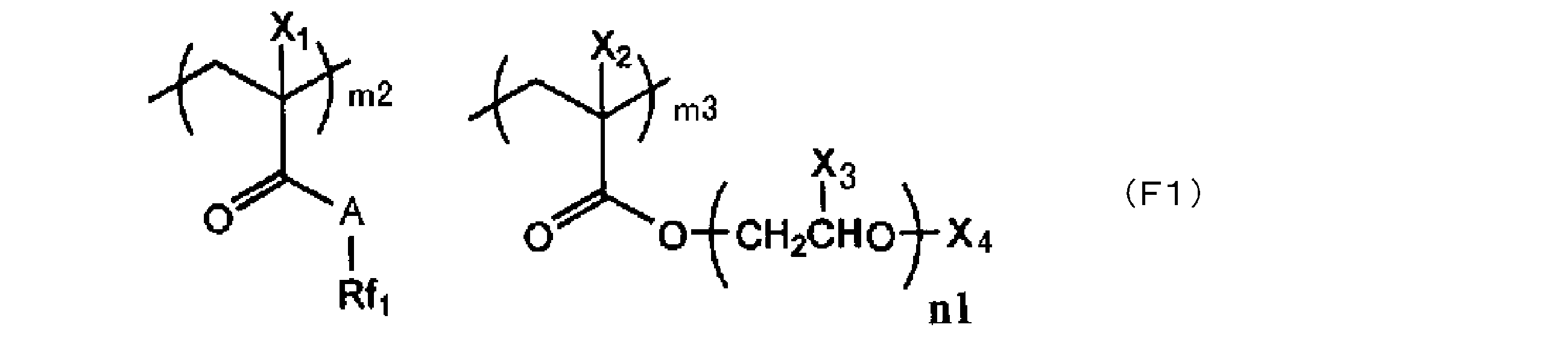
Aは、酸素原子、硫黄原子又は-NR-を表す。式中、Rは、水素原子またはアルキル基を表す。
X1、X2、X3、X4及びRのアルキル基は、炭素原子数1~12が好ましく、1~6がより好ましく、1~3が特に好ましい。例えば、メチル基、エチル基、プロピル基、i-プロピル基、ブチル基、i-ブチル基、t-ブチル基等を挙げることができる。
m2及びm3は、各々独立に、1~100の整数を表す。
n1は、1~20の整数を表す。n1が2以上である場合、X3は同一でも異なっていてもよく、エチレンオキシ基とプロピレンオキシ基とが存在して構成されることが好ましい。なお、アルキレンオキシ基が分岐状である場合、分岐位置は上記式で示される酸素と連結する炭素で分岐する態様でも、酸素から離れた炭素で分岐している態様でも、どちらでもよい。実際には、分岐位置が異なるアルキレンオキシ基の混合物となる。
Rf1は、フルオロアルキル基を表す。
本発明の光学機能層形成用組成物中における界面活性剤の含有量は、組成物中の固形分に対して0.01質量%以上が好ましく、0.05質量%以上がより好ましく、0.1質量%以上が特に好ましい。上限としては、1質量%以下が好ましく、0.75質量%以下がより好ましく、0.5質量%以下が特に好ましい。
界面活性剤の含有量を上記下限値以上とすることで、スジ状の塗布欠陥を改良することができ好ましい。上記上限値以下とすることで、相溶性を良化することができ好ましい。
界面活性剤は、1種のみを用いてもよいし、2種類以上を組み合わせてもよい。
本発明においては、光学機能層形成用組成物に分散剤を用いることも好ましい。
分散剤としては、高分子分散剤(例えば、ポリアミドアミンとその塩、ポリカルボン酸とその塩、高分子量不飽和酸エステル、変性ポリウレタン、変性ポリエステル、変性ポリ(メタ)アクリレート、(メタ)アクリル系共重合体、ナフタレンスルホン酸ホルマリン縮合物)、及び、ポリオキシエチレンアルキルリン酸エステル、ポリオキシエチレンアルキルアミン、アルカノールアミン、顔料誘導体等を挙げることができる。
高分子分散剤は、その構造から更に直鎖状高分子、末端変性型高分子、グラフト型高分子、ブロック型高分子に分類することができる。
これらの分散剤は、単独で使用してもよく、2種以上を組み合わせて使用してもよい。
本発明の光学機能層形成用組成物には、先にコロイダルシリカの粒子液(ゾル)の調製溶媒として述べたものとともに、またはそのほかに、さらに溶媒を含有させてもよい。あるいは、調製溶媒を切り替えて下記の溶媒を含むものとしてもよい。組成物に含まれる溶媒としては、たとえば、有機溶媒(脂肪族化合物、ハロゲン化炭化水素化合物、アルコール化合物、エーテル化合物、エステル化合物、ケトン化合物、ニトリル化合物、アミド化合物、スルホキシド化合物、芳香族化合物)または水が挙げられる。それぞれの例を下記に列挙する。
・脂肪族化合物
ヘキサン、ヘプタン、シクロヘキサン、メチルシクロヘキサン、オクタン、ペンタン、シクロペンタンなど
・ハロゲン化炭化水素化合物
塩化メチレン、クロロホルム、ジクロルメタン、二塩化エタン、四塩化炭素、トリクロロエチレン、テトラクロロエチレン、エピクロロヒドリン、モノクロロベンゼン、オルソジクロロベンゼン、アリルクロライド、ハイドロクロロフルオロカーボン(HCFC)、モノクロロ酢酸メチル、モノクロロ酢酸エチル、モノクロロ酢酸トリクロル酢酸、臭化メチル、ヨウ化メチル、トリ(テトラ)クロロエチレンなど
・アルコール化合物
メチルアルコール、エチルアルコール、1-プロピルアルコール、2-プロピルアルコール、2-ブタノール、エチレングリコール、プロピレングリコール、グリセリン、1,6-ヘキサンジオール、シクロヘキサンジオール、ソルビトール、キシリトール、2-メチル-2,4-ペンタンジオール、1,3-ブタンジオール、1,4-ブタンジオールなど
・エーテル化合物(水酸基含有エーテル化合物を含む)
ジメチルエーテル、ジエチルエーテル、ジイソプロピルエーテル、ジブチルエーテル、t-ブチルメチルエーテル、シクロヘキシルメチルエーテル、アニソール、テトラヒドロフラン、アルキレングリコールアルキルエーテル(エチレングリコールモノメチルエーテル、エチレングリコールモノブチルエーテル、ジエチレングリコール、ジプロピレングリコール、プロピレングリコールモノメチルエーテル、ジエチレングリコールモノメチルエーテル、トリエチレングリコール、ポリエチレングリコール、プロピレングリコールモノメチルエーテル、ジプロピレングリコールモノメチルエーテル、トリプロピレングリコールモノメチルエーテル、ジエチレングリコールモノブチルエーテル、ジエチレングリコールモノブチルエーテル等)など
・エステル化合物
酢酸エチル、乳酸エチル、2-(1-メトキシ)プロピルアセテート、プロピレングリコールモノメチルエーテルアセテート、3-エトキシプロピオン酸エチルなど
・ケトン化合物
アセトン、メチルエチルケトン、メチルイソブチルケトン、シクロヘキサノン、2-ヘプタノンなど
・ニトリル化合物
アセトニトリルなど
・アミド化合物
N,N-ジメチルホルムアミド、1-メチル-2-ピロリドン、2-ピロリジノン、1,3-ジメチル-2-イミダゾリジノン、2-ピロリジノン、ε-カプロラクタム、ホルムアミド、N-メチルホルムアミド、アセトアミド、N-メチルアセトアミド、N,N-ジメチルアセトアミド、N-メチルプロパンアミド、ヘキサメチルホスホリックトリアミドなど
・スルホキシド化合物
ジメチルスルホキシドなど
・芳香族化合物
ベンゼン、トルエンなど
好ましい溶媒としては、なかでも、メチルアルコール、エチルアルコール、2-プロピルアルコール、プロピレングリコールモノメチルエーテル、酢酸エチル、プロピレングリコール-1-モノメチルエーテル-2-アセテート、乳酸エチル、3-エトキシプロピオン酸エチル、シクロヘキサノンが挙げられる。
好ましい より好ましい 特に好ましい
非プロトン性極性溶媒 10%~100% 30%~100% 50%~100%
プロトン性極性溶媒 0 ~ 50% 0 ~ 30% 0 ~ 5%
水 0 ~ 30% 0 ~ 10% 0 ~ 2%
本発明の光学機能層形成用組成物には重合性化合物を含有させてもよい。重合性化合物は、そのClogP値が2以上であることが好ましく、2~10であることがより好ましい。上記のClogP値が小さすぎると、十分な解像度が得られず、微細な画素を形成する際に、その端部等に欠けや割れが生じたりすることがある。逆にClogP値が大きすぎると粘稠になり、加工性に劣ることがある。あるいは、硬化膜の表面が荒れた状態となることがある。
本明細書において化合物のClogP値は下記の定義による。
オクタノール-水分配係数(logP値)の測定は、一般にJIS日本工業規格Z7260-107(2000)に記載のフラスコ浸とう法により実施することができる。また、オクタノール-水分配係数(logP値)は実測に代わって、計算化学的手法あるいは経験的方法により見積もることも可能である。計算方法としては、Crippen’s fragmentation法(J.Chem.Inf.Comput.Sci.,27,21(1987))、Viswanadhan’s fragmentation法(J.Chem.Inf.Comput.Sci.,29,163(1989))、Broto’s fragmentation法(Eur.J.Med.Chem.-Chim.Theor.,19,71(1984))などを用いることが知られている。本発明では、Crippen’s fragmentation法(J.Chem.Inf.Comput.Sci.,27,21(1987))を用いる。
ClogP値とは、1-オクタノールと水への分配係数Pの常用対数logPを計算によって求めた値である。ClogP値の計算に用いる方法やソフトウェアについては公知の物を用いることができる。特に断らない限り、本発明ではDaylight Chemical Information Systems社のシステム:PCModelsに組み込まれたClogPプログラムを用いることとする。
これらの具体的な化合物としては、特開2009-288705号公報の段落番号[0095]~段落番号[0108]に記載されている化合物を本発明においても好適に用いることができる。
多官能カルボン酸にグリシジル(メタ)アクリレート等の環状エーテル基とエチレン性不飽和基を有する化合物を反応させて得られる多官能(メタ)アクリレートなども挙げることができる。
また、その他の好ましい重合性化合物として、特開2010-160418号公報、特開2010-129825号公報、特許4364216号公報等に記載される、フルオレン環を有し、エチレン性重合性基を2官能以上有する化合物、カルド樹脂も使用することが可能である。
(反応性基RA:ビニル基、(メタ)アクリロイル基、または(メタ)アクリロイルオキシ基。)


上記ラジカル重合性モノマーの具体例としては、特開2007-269779号公報の段落番号[0248]~段落番号[0251]に記載されている化合物を本実施形態においても好適に用いることができる。
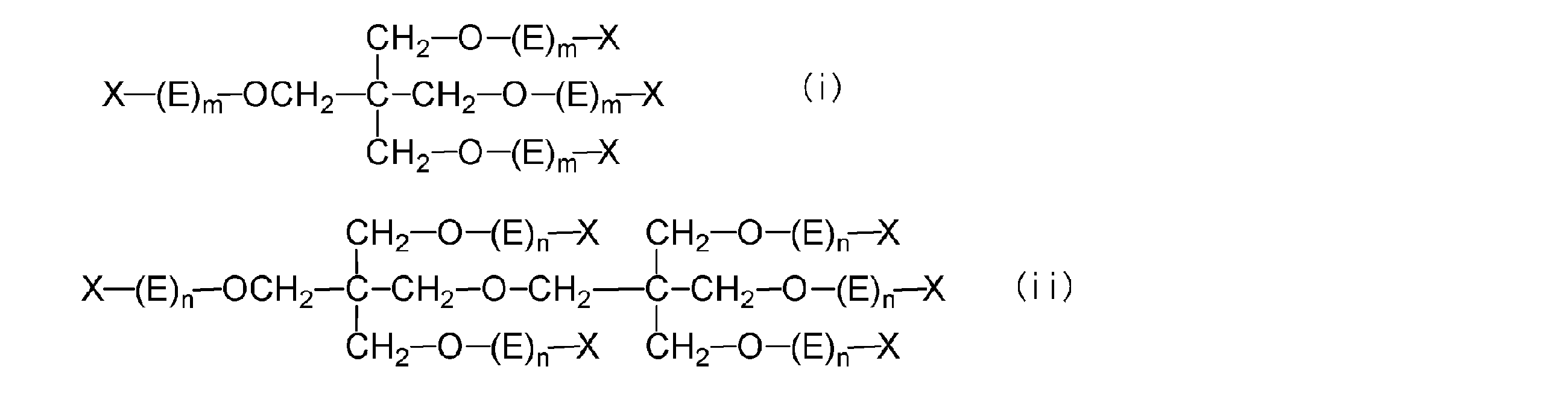
yは、それぞれ、1~10の整数を表し、1~5の整数が好ましく、1~3がより好ましい。
Xは、それぞれ、水素原子、アクリロイル基、メタクリロイル基、または、カルボキシル基を表す。
式(i)中、アクリロイル基およびメタクリロイル基の合計は3個または4個であることが好ましく、4個がより好ましい。
mは、それぞれ、0~10の整数を表し、1~5が好ましい。それぞれのmの合計は1~40の整数であり、4個~20個が好ましい。
式(ii)中、アクリロイル基およびメタクリロイル基の合計は5個または6個であることが好ましく、6個がより好ましい。
nは、それぞれ、0~10の整数を表し、1~5が好ましい。それぞれnの合計は1~60の整数であり、4個~30個が好ましい。



重合性化合物の市販品としては、ウレタンオリゴマーUAS-10、UAB-140(日本製紙株式会社(旧山陽国策パルプ株式会社)製)、UA-7200(新中村化学工業株式会社製)、DPHA-40H(日本化薬株式会社製)、UA-306H、UA-306T、UA-306I、AH-600、T-600、AI-600(共栄社化学株式会社製)などが挙げられる。
重合性化合物は分子量が10,000以下であることが好ましく、5,000以下であることがより好ましく、2,000以下であることがより好ましく、1,000以下であることが特に好ましい。下限値は、200以上であることが実際的である。
なお、本明細書において、「アクリル」というときにはアクリロイル基を有する構造群を広く指し、例えば、α位に置換基を有する構造を含むものとする。ただし、α位にメチル基を有するものをメタクリルと呼び、これを含む意味で(メタ)アクリルなどと称することもある。
本発明の光学機能層形成用組成物は、密着改良剤をさらに含有していてもよい。密着改良剤としては、例えば、特開平5-11439号公報、特開平5-341532号公報、及び特開平6-43638号公報等に記載の密着改良剤が好適挙げられる。具体的には、ベンズイミダゾール、ベンズオキサゾール、ベンズチアゾール、2-メルカプトベンズイミダゾール、2-メルカプトベンズオキサゾール、2-メルカプトベンズチアゾール、3-モルホリノメチル-1-フェニル-トリアゾール-2-チオン、3-モルホリノメチル-5-フェニル-オキサジアゾール-2-チオン、5-アミノ-3-モルホリノメチル-チアジアゾール-2-チオン、及び2-メルカプト-5-メチルチオ-チアジアゾール、トリアゾール、テトラゾール、ベンゾトリアゾール、カルボキシベンゾトリアゾール、アミノ基含有ベンゾトリアゾール、シランカップリング剤などが挙げられる。密着改良剤としては、シランカップリング剤が好ましい。
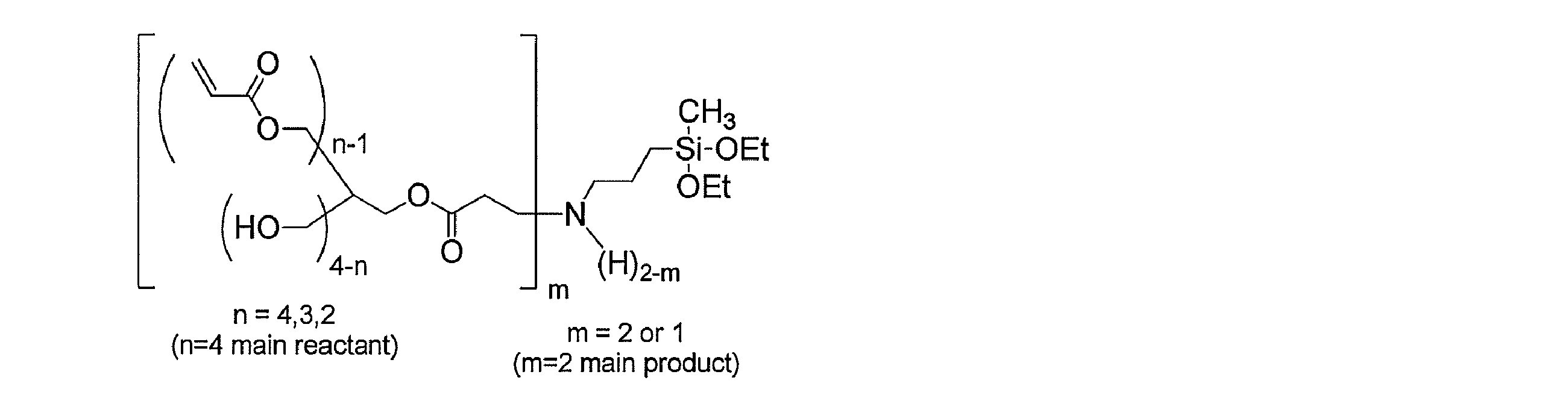
本明細書において置換・無置換を明記していない置換基(連結基についても同様)については、その基に任意の置換基を有していてもよい意味である。これは置換・無置換を明記していない化合物についても同義である。好ましい置換基としては、下記置換基Tが挙げられる。
置換基Tとしては、下記のものが挙げられる。
アルキル基(好ましくは炭素原子数1~20のアルキル基、例えばメチル、エチル、イソプロピル、t-ブチル、ペンチル、ヘプチル、1-エチルペンチル、ベンジル、2-エトキシエチル、1-カルボキシメチル等)、アルケニル基(好ましくは炭素原子数2~20のアルケニル基、例えば、ビニル、アリル、オレイル等)、アルキニル基(好ましくは炭素原子数2~20のアルキニル基、例えば、エチニル、ブタジイニル、フェニルエチニル等)、シクロアルキル基(好ましくは炭素原子数3~20のシクロアルキル基、例えば、シクロプロピル、シクロペンチル、シクロヘキシル、4-メチルシクロヘキシル等)、アリール基(好ましくは炭素原子数6~26のアリール基、例えば、フェニル、1-ナフチル、4-メトキシフェニル、2-クロロフェニル、3-メチルフェニル等)、ヘテロ環基(好ましくは炭素原子数2~20のヘテロ環基、好ましくは、少なくとも1つの酸素原子、硫黄原子、窒素原子を有する5または6員環のヘテロ環基が好ましく、例えば、2-ピリジル、4-ピリジル、2-イミダゾリル、2-ベンゾイミダゾリル、2-チアゾリル、2-オキサゾリル等)、アルコキシ基(好ましくは炭素原子数1~20のアルコキシ基、例えば、メトキシ、エトキシ、イソプロピルオキシ、ベンジルオキシ等)、アリールオキシ基(好ましくは炭素原子数6~26のアリールオキシ基、例えば、フェノキシ、1-ナフチルオキシ、3-メチルフェノキシ、4-メトキシフェノキシ等)、アルコキシカルボニル基(好ましくは炭素原子数2~20のアルコキシカルボニル基、例えば、エトキシカルボニル、2-エチルヘキシルオキシカルボニル等)、アミノ基(好ましくは炭素原子数0~20のアミノ基、アルキルアミノ基、アリールアミノ基を含み、例えば、アミノ、N,N-ジメチルアミノ、N,N-ジエチルアミノ、N-エチルアミノ、アニリノ等)、スルファモイル基(好ましくは炭素原子数0~20のスルファモイル基、例えば、N,N-ジメチルスルファモイル、N-フェニルスルファモイル等)、アシル基(好ましくは炭素原子数1~20のアシル基、例えば、アセチル、プロピオニル、ブチリル、ベンゾイル等)、アシルオキシ基(好ましくは炭素原子数1~20のアシルオキシ基、例えば、アセチルオキシ、ベンゾイルオキシ等)、カルバモイル基(好ましくは炭素原子数1~20のカルバモイル基、例えば、N,N-ジメチルカルバモイル、N-フェニルカルバモイル等)、アシルアミノ基(好ましくは炭素原子数1~20のアシルアミノ基、例えば、アセチルアミノ、ベンゾイルアミノ等)、スルホンアミド基(好ましくは炭素原子数0~20のスルホンアミド基、例えば、メタンスルホンアミド、ベンゼンスルホンアミド、N-メチルメタンスルホンアミド、N-エチルベンゼンスルホンアミド等)、アルキルチオ基(好ましくは炭素原子数1~20のアルキルチオ基、例えば、メチルチオ、エチルチオ、イソプロピルチオ、ベンジルチオ等)、アリールチオ基(好ましくは炭素原子数6~26のアリールチオ基、例えば、フェニルチオ、1-ナフチルチオ、3-メチルフェニルチオ、4-メトキシフェニルチオ等)、アルキルもしくはアリールスルホニル基(好ましくは炭素原子数1~20のアルキルもしくはアリールスルホニル基、例えば、メチルスルホニル、エチルスルホニル、ベンゼンスルホニル等)、ヒドロキシ基、シアノ基、ハロゲン原子(例えばフッ素原子、塩素原子、臭素原子、ヨウ素原子等)である。
また、これらの置換基Tで挙げた各基は、上記の置換基Tがさらに置換していてもよい。上記のアルキル基、アルケニル基、アルキニル基は(これらを含む基を含む)、分岐状であっても、直鎖状であってもよい。また、環状であっても、非環状であってもよい。なお、隣接する置換基や連結基は、本発明の効果を損ねない範囲で、互いに結合して環を形成していてもよい。
本明細書において、化合物の置換基や連結基の選択肢を始め、温度、厚さといった各技術事項は、そのリストがそれぞれ独立に記載されていても、相互に組み合わせることができる。
本発明の光学機能層形成用組成物は、異物の除去や欠陥の低減などの目的で、フィルタで濾過することが好ましい。従来からろ過用途等に用いられているものであれば特に限定されることなく用いることができる。例えば、PTFE(ポリテトラフルオロエチレン)等のフッ素樹脂、ナイロン等のポリアミド系樹脂、ポリエチレン、ポリプロピレン(PP)等のポリオレフィン樹脂(高密度、超高分子量を含む)等によるフィルタが挙げられる。これら素材の中でもポリプロピレン(高密度ポリプロピレンを含む)及びナイロンが好ましい。
フィルタの孔径は、0.1μm~7μm程度が適しており、好ましくは0.2μm~2.5μm程度、より好ましくは0.2μm~1.5μm程度、さらに好ましくは0.3μm~0.7μmである。この範囲とすることにより、ろ過詰まりを抑えつつ、不純物や凝集物など、微細な異物をより確実に除去することが可能となる。
フィルタを使用する際、異なるフィルタを組み合わせてもよい。その際、第1のフィルタでのフィルタリングは、1回のみでもよいし、2回以上行ってもよい。異なるフィルターを組み合わせて2回以上フィルタリングを行う場合は1回目のフィルタリングの孔径より2回目以降の孔径が同じ、もしくは大きい方が好ましい。また、上述した範囲内で異なる孔径の第1のフィルタを組み合わせてもよい。ここでの孔径は、フィルタメーカーの公称値を参照することができる。市販のフィルタとしては、例えば、日本ポール株式会社、アドバンテック東洋株式会社、日本インテグリス株式会社(旧日本マイクロリス株式会社)又は株式会社キッツマイクロフィルタ等が提供する各種フィルタの中から選択することができる。
第2のフィルタは、上述した第1のフィルタと同様の材料等で形成されたものを使用することができる。第2のフィルタの孔径は、0.2μm~10.0μm程度が適しており、好ましくは0.2μm~7.0μm程度、さらに好ましくは0.3μm~6.0μm程度である。この範囲とすることにより、混合液に含有されている成分粒子を残存させたまま、混合液に混入している異物を除去することができる。
例えば、第1のフィルタでのフィルタリングは、分散液のみで行い、他の成分を混合した後で、第2のフィルタリングを行ってもよい。
本発明の光学機能層は、光学機能層を形成する工程(塗布工程、プリベーク工程、膜を硬化させる工程(ポストベーク工程))と、上記光学機能層にレジストを付与する工程と、上記レジストに対してパターン露光して現像する工程と、上記レジストをマスクとして上記光学機能層をエッチング加工する工程と、残存する上記レジストをドライ処理により除去する工程とを介して形成されることが好ましい(図2参照)。以下にその他の工程も併せて、各工程の詳細について説明する。
本発明の光学機能層形成用組成物は、これを用いて光学製品等に適用される光学機能層とすることが好ましい。本発明において、支持体上への光学機能層形成用組成物の適用方法としては、塗布法によることが好ましい。具体的には、スリット塗布、インクジェット法、回転塗布、流延塗布、ロール塗布、スクリーン印刷法等の各種の塗布方法を適用することができる。上記光学機能層は、コロイダルシリカ粒子と界面活性剤とを含有する光学機能層形成用組成物を硬化させてなることが好ましい。支持体としては、例えば、基板(例えば、シリコン基板)上にCCD(Charge Coupled Device)やCMOS(Complementary Metal-Oxide Semiconductor)等の撮像素子(受光素子)が設けられた固体撮像素子用基板を用いることができる。固体撮像素子用基板における各撮像素子間や、固体撮像素子用基板の裏面には、遮光膜が設けられていてもよい。また、支持体上には、必要により、上部の層との密着改良、物質の拡散防止或いは基板表面の平坦化のために下塗り層を設けてもよい。
支持体上に塗布された光学機能層形成用組成物層の乾燥(プリベーク)は、ホットプレート、オーブン等で50℃~140℃の温度で10秒~300秒で行うことができる。
本実施形態においては、次いで、加熱処理(ポストベーク)を行うことが好ましい。ポストベークは、硬化を完全なものとするための現像後の加熱処理である。その加熱温度は、有機光電変換部の損傷を抑制する観点から、250℃以下が好ましく、240℃以下がより好ましく、230℃以下がさらに好ましい。下限は特になく、効率的かつ効果的な処理を考慮すると、50℃以上の熱硬化処理を行うことが好ましく、100℃以上がより好ましい。
このポストベーク処理は、現像後の塗布膜を、上記条件になるようにホットプレートやコンベクションオーブン(熱風循環式乾燥機)、高周波加熱機等の加熱手段を用いて、連続式あるいはバッチ式で行うことができる。
本発明の好ましい実施形態においては、上記の光学機能層形成用組成物の塗布膜にレジストを付与し、そこに露光エネルギーを照射し、その露光部分を現像してパターンを形成する。
更に、いわゆる化学増幅系レジストを用いることも可能である。化学増幅系レジストについては、例えば、「光機能性高分子材料の新展開 1996年5月31日 第1刷発行 監修:市村國宏、発行所:株式会社シーエムシー」の129ページ以降に説明されているレジストを挙げることができる(特に、131ページ付近に説明されている、ポリヒドロキシスチレン樹脂の水酸基を酸分解性基で保護した樹脂を含むレジストや、同じく131ページ付近に説明されているESCAP型のレジストなどが好ましい)。より具体的には、特開2008-268875号公報、特開2008-249890号公報、特開2009-244829号公報、特開2011-013581号公報、特開2011-232657号公報、特開2012-003070号公報、特開2012-003071号公報、特許第3638068号公報、特許第4006492号公報、特許第4000407号公報、特許第4194249号公報の実施例等に記載されたレジストを用いることができる。これら文献は本明細書中に組み込まれる。
本実施形態では、次いでアルカリ現像処理等の現像を行う。これにより、ネガ型であれば、露光工程における光未照射部分のレジストがアルカリ水溶液に溶出し、光硬化した部分だけが残る。現像液としては、下地の撮像素子や回路などにダメージを起さない、有機アルカリ現像液が望ましい。現像温度としては通常20℃~30℃であり、現像時間は、例えば、20秒~90秒である。より残渣を除去するため、近年では120秒~180秒実施する場合もある。さらには、より残渣除去性を向上するため、現像液を60秒ごとに振り切り、さらに新たに現像液を供給する工程を数回繰り返す場合もある。
アルカリ性化合物は、例えば、水酸化ナトリウム、水酸化カリウム、炭酸ナトリウム,硅酸ナトリウム、メタ硅酸ナトリウム、アンモニア水、エチルアミン、ジエチルアミン、ジメチルエタノールアミン、テトラメチルアンモニウムヒドロキシド、テトラエチルアンモニウムヒドロキシド、テトラプロピルアンモニウムヒドロキシド、テトラブチルアンモニウムヒドロキシ、ベンジルトリメチルアンモニウムヒドロキシド、コリン、ピロール、ピペリジン、1,8-ジアザビシクロ[5.4.0]-7-ウンデセン等が挙げられる(このうち、有機アルカリが好ましい。)。
なお、アルカリ性水溶液を現像液として用いた場合は、一般に現像後に水で洗浄処理が施される。
光学機能層のエッチングは、ドライエッチングであっても、ウエットエッチングであってもよい。ドライエッチングとしては、例えば、フッ素系ガスとO2との混合比率(フッ素系ガス/O2)が流量比で4/1~1/5である混合ガスを用いたドライエッチング法により行うことができる(フッ素系ガスと酸素の比率はフッ素系ガスのC含有量による)。ドライエッチング法の代表的な例としては、特開昭59-126506号、特開昭59-46628号、特開昭58-9108号、特開昭58-2809号、特開昭57-148706号、特開昭61-41102号などの公報に記載されているような方法が知られている。
CnHmFl 式(I)
〔式中、nは、1~6、mは、0~13、lは、1~14を表わす。〕
本発明の光学機能層形成用組成物で形成された光学機能層の屈折率は、1.5以下であることが好ましく、1.4以下であることがより好ましく、1.3以下であることがさらに好ましく、1.24以下であることが特に好ましい。下限は、1.1以上であることが実際的である。なお、本明細書において膜の屈折率は、特に断らない限り、波長633nmの光を用いて、25℃で測定した値とする。
本発明においては、上記の光学機能層に表面密着処理を施すことが好ましい。例えば、光学機能層のポストベーク膜を形成した後に、その表面に密着処理を施し、疎水性の表面とすることが好ましい。次いで、レジストを付与するという手順である。
密着処理としては、例えば、HMDS処理を挙げることができる。この処理には、HMDS(ヘキサメチレンジシラザン、Hexamethyldisilazane)が用いられる。HMDSを例えば上述したSiO2を含有する層に適用すると、その表面に存在するSi-OH結合と反応し、Si-O-Si(CH3)3を生成すると考えられる。これにより、膜表面を疎水化することができる。このように光学機能層の表面を疎水化することにより、引き続くレジストのパターニングの工程において、現像液の侵入を防ぎ、損傷を抑制・防止することができる。
本発明の好ましい実施形態であるマイクロレンズユニットは、上記光学機能層とこれに被覆されたマイクロレンズとを具備した積層構造を有する。このレンズユニットは、固体撮像素子(光学デバイス)に組み込まれる。
本発明の好ましい実施形態に係る固体撮像素子においては、上記光学機能層形成用組成物で形成した光学機能層をマイクロレンズ上の反射防止膜、中間膜、またはカラーフィルタの隔壁、カラーフィルタ層の額縁、カラーフィルター層に配置されるグリッド構造に適用することができる。固体撮像素子の構造は、例えば、シリコン基板の上に設けられた受光素子(フォトダイオード)、下部平坦化膜、カラーフィルター、上部平坦化膜、マイクロレンズ等から構成される。カラーフィルターは赤(R)、緑(G)、青(B)の各カラーフィルター画素部で構成されている。カラーフィルターは、2次元配列された複数の緑色画素部で構成されている。各着色画素部は、それぞれ受光素子の上方位置に形成されている。緑色画素部がBayerパターン(市松模様)に形成されるとともに、青色画素部及び赤色画素部は、緑色画素部の間に形成されている。
平坦化膜は、カラーフィルターの上面を覆うように形成されており、カラーフィルター表面を平坦化している。マイクロレンズは、凸面を上にして配置された集光レンズであり、平坦化膜の上方でかつ受光素子の上方に設けられている。すなわち、光の入射方向に沿って、マイクロレンズ、カラーフィルター画素部および受光素子が直列に並ぶ配置とされ、外部からの光を効率良く各受光素子へ導く構造とされている。なお、受光素子およびマイクロレンズについて、この種の固体撮像素子に通常適用されるものを適宜利用することができる。よって、詳細な説明を省略する。
本発明の組成物で形成した光学機能層は、上記の固体撮像素子に好適に適用することができる。
上記カラーフィルター層に配置されたグリッド構造(隔壁)の例としては、特開2012-227478号公報、特開2010-0232537号公報、特開2009-111225号公報の例示構造が挙げられる。その一実施形態を下記に示す。本実施形態に係る固体撮像装置においては、受光部としてフォトダイオードが形成された半導体基板、半導体基板上に形成された絶縁膜、及び絶縁膜上の隣接するフォトダイオードの間に相当する箇所に立設された隔壁を備える。さらに、固体撮像装置は、絶縁膜上であって隣接する隔壁の間に形成されたカラーフィルター、隔壁上面上と隔壁側面上とから絶縁膜上に拡がる密着層、及びカラーフィルター上に形成されたマイクロレンズを備える。絶縁膜内には、配線が埋設されており、これらの積層体が、配線層に該当する。なお、隔壁を平面視すると格子状となっており、隔壁の正方形状の開口にカラーフィルターが形成されている。カラーフィルターは、ここでは、赤(R)、緑(G)、青(B)の3種類あり、例えば、ベイヤー配列されている。
本実施形態のカラーフィルター周辺の額縁構造としては、特開2014-048596号公報に記載の例示構造を挙げることができる。本実施形態においては、ガラス基板からなる透明基板を基材として、上記基材の一面側において、表示用領域にカラーフィルター用の各色の着色層と画素区分用遮光部を配している。且つ、上記表示用領域の外側に非表示用領域として遮光性の額縁部を設けており、表示用領域の着色層と、額縁部とを覆うように平坦状に保護層を配している。
(1)コロイダルシリカ粒子液の調製
先ず、ケイ素アルコキシド(A)としてテトラエトキシシラン(TEOS)を、フルオロアルキル基含有のケイ素アルコキシド(B)としてトリフルオロプロピルトリメトキシシラン(TFPTMS)を用意する。ケイ素アルコキシド(A)の質量を1としたときのフルオロアルキル基含有のケイ素アルコキシド(B)の割合(質量比)が0.6になるように秤量し、これらをセパラブルフラスコ内に投入して混合することにより混合物を得た。この混合物1質量部に対して1.0質量部となる量のプロピレングリコールモノメチルエーテル(PGME)を有機溶媒(E)として添加し、30℃の温度で15分間撹拌することにより第1液を調製した。
また、この第1液とは別に、混合物1質量部に対して1.0質量部となる量のイオン交換水(C)と0.01質量部となる量のギ酸(D)をビーカー内に投入して混合し、30℃の温度で15分間撹拌することにより第2液を調製した。次に、上記調製した第1液を、ウォーターバスにて55℃の温度に保持してから、この第1液に第2液を添加し、上記温度を保持した状態で60分間撹拌した。これにより、上記ケイ素アルコキシド(A)と上記フルオロアルキル基含有のケイ素アルコキシド(B)との加水分解物(F)を得た。
この液の固形分濃度は、SiO2換算で10質量%であった。
次に、市販の平均直径15nmのコロイダルシリカ(日産化学工業株式会社製、商品名ST-30)が30質量%含まれる水分散液に、硝酸カルシウム水溶液30質量%を0.1質量部加えた混合液を、ステンレス製オートクレーブ中で120℃5時間加熱した。この分散液に対し、限外濾過法を用い、溶媒をプロピレングリコールモノメチルエーテルに置換し、更にホモミクサー(プライミクス社製)を用いて回転速度14000rpmにて30分間攪拌し、十分に分散させ、更にプロピレングリコールモノメチルエーテルを添加して、固形分濃度15質量%のコロイダルシリカ粒子液(G)を得た。
ケイ素アルコキシドの加水分解物(F)30質量部と、コロイダルシリカ粒子液(G)70質量部を混合し、更に40℃で10時間加熱し、1000Gで10分間遠心分離を行って沈降物を除去することで、コロイダルシリカ粒子液P1を得た。その他、下記表1のコロイダルシリカ粒子液を適宜製造条件や原料を変えて調製した。
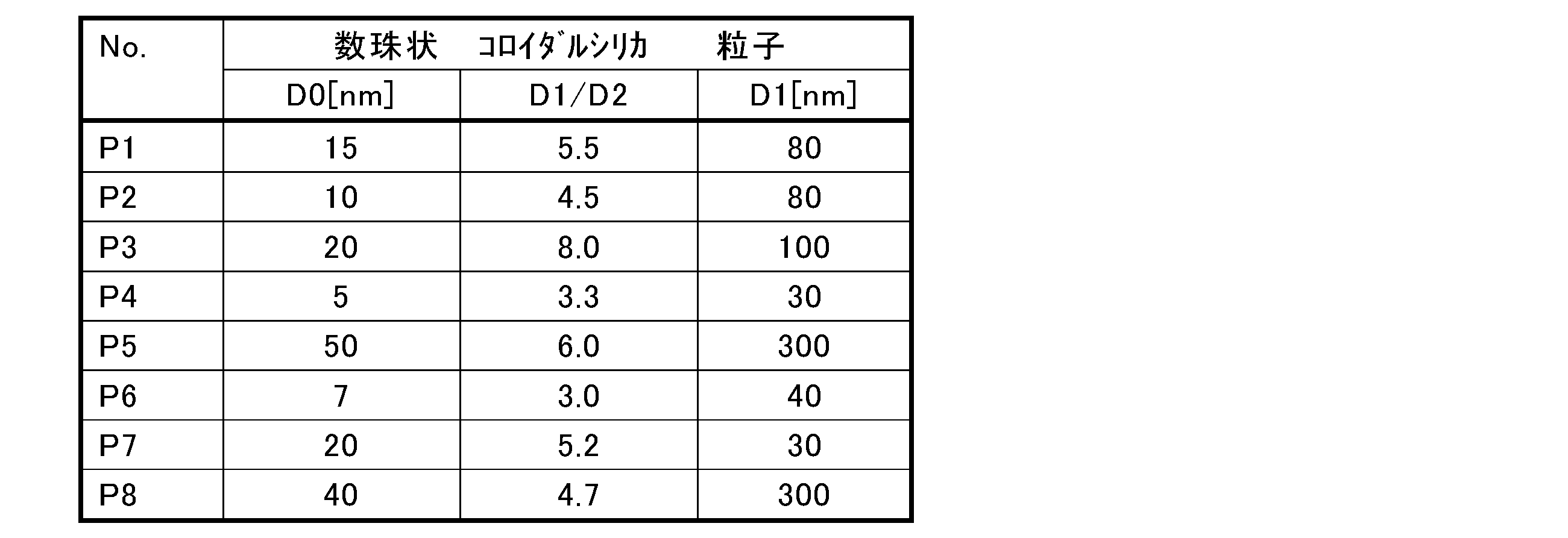
D1:動的光散乱法により測定されたコロイダルシリカ粒子の数平均粒子径
D2:比表面積より求めたコロイダルシリカ粒子の平均粒子径
上記で得られたコロイダルシリカ粒子液を用いて、以下の表2の組成となるように各成分を混合して光学機能層形成用組成物を得た。なお、上記のコロイダルシリカの粒子液の調製後、及び光学機能層形成用組成物の調製後それぞれについて、全て日本ポール社製のDFA4201NXEY(0.45μmナイロンフィルター)を用いてろ過を行った。
上記で得られた光学機能層形成用組成物を、塗布後の膜厚が0.6μmになるように、ブランク基板(シリコンウェハ)上にスピンコート法で塗布した。その後、ホットプレート上で、100℃で2分間加熱して上記組成物の硬化膜を得た。得られた硬化膜について、下記の評価を行った。結果を下記表2に示す。なお、膜の透明性(透過率)についても評価し、本実施例の硬化膜は均質で良好な透明性を有することを確認した。
得られた膜の面状(ストリエーションの状態)をオリンパス株式会社製半導体検査顕微鏡MX50光学顕微鏡にて50倍の倍率で観察した。
結果を下記に区分して判定した。
4: スジ状のムラが、膜全体で全くない
3: スジ状のムラが、膜全体で3本未満
2: スジ状のムラが、膜全体で3本以上10本未満あり、実用不可能
1: スジ状のムラが、膜全体で10本以上あり、実用不可能
試験c01(比較例)の顕微鏡像を図3に載せた。
得られた膜の屈折率をエリプソメータ(ジェー・エー・ウーラム社製VUV-vase[商品名])で測定した(波長633nm、測定温度25℃)。
得られた膜をエスペック社製の高度加速寿命試験装置EHS-221(M)にて温度85℃,湿度95%RHの環境下に20時間曝し、屈折率測定を実施した。
結果を下記に区分して判定した。
4: 耐湿評価前後の屈折率差が0.003未満
3: 耐湿評価前後の屈折率差が0.003以上0.005未満
2: 耐湿評価前後の屈折率差が0.005以上0.01未満
1: 耐湿評価前後の屈折率差が0.01以上
得られた膜のヤング率を、MTS Systems社製のナノインデンターSA2を使用して測定した。測定温度は室温(約25℃)とした。

配合は質量部である
LC-OH:エタノール、メタノール
EL:乳酸エチル
PG:プロピレングリコール
PGME:プロピレングリコールモノメチルエーテル
PGMEA:プロピレングリコールモノメチルエーテルアセテート
DPG:ジプロピレングリコール
F781F:メガファック (DIC社製 商品名)・・・下記化学式参照
F554:メガファック (DIC社製 商品名)
F559:メガファック (DIC社製 商品名)
EC-080:EMULSOGEN COL-080
(クラリアント社製 商品名)
アニオン界面活性剤:
(R-O-(EO)8-COOH,
Rは炭素数18のオレイル基、EOはエチレンオキシ基)
PAA-03:ポリアリルアミン-03
(スペシャリティケミカルス事業部
ニットーボーメディカル株式会社製 商品名)
カチオン高分子界面活性剤 重量平均分子量 3000

上記構造中、EOはエチレンオキシ基、POはプロピレンオキシ基を表す。
p、q、rは整数を表す。分子量は、12500。
M305:東亜合成株式会社製(商品名)
A-TMMT:新中村化学工業株式会社製(商品名)
コロイダルシリカ粒子液P1に対して、SiO2で同量となるようにスルーリア2320(日揮触媒化成株式会社製の中空シリカの20質量%MIBK(メチルイソブチルケトン)分散液)を配合した。それ以外同様にして、光学機能層形成用組成物cP1を調製した。
コロイダルシリカ粒子液P1に対して、ケイ素アルコキシドの加水分解物(F)を用いなかった以外同様にして、光学機能層形成用組成物cP2を調製した。ただし、固形分中のSiO2分の量は試験101と同じになるように調整した。
上記の試験101の粒子液P1をそれぞれP2~P8に代え、同様に、各項目の測定・評価を行った。その結果は、面状が3~4、屈折率が1.24以下、耐湿評価が4、ヤング率が5.0~6.0の良好な結果であった。
試験101~112の光学機能層形成用組成物(各粒子液)にトリエチレングリコールモノブチルエーテル(沸点271℃)を15質量部で添加した。その結果、各粒子液の乾燥性が抑えられ、製造適正および製造品質がともに向上することを確認した。
上記試験101で得られた光学機能層形成用組成物を、塗布後の膜厚が0.6μmになるように、下塗り層付きシリコンウェハ上にスピンコート法で塗布し、その後ホットプレート上で、100℃で2分間加熱、さらに、ホットプレート上で、230℃で10分間加熱して光学機能層形成用組成物層を得た。
次いで、得られた光学機能層形成用組成物層に対し、HMDS処理(200℃×1minのBake、110℃×1minHMDS vapor)を実施した後、ポジ型フォトレジスト(富士フイルムエレクトロニクスマテリアルズ株式会社製、商品名FHi622BC)をスピンコーターにて塗布し、100℃で2分間の加熱処理を行い、膜厚が1.0μmの厚さになるようにフォトレジスト層を形成した。次に、i線ステッパー露光装置FPA-3000i5+(キヤノン株式会社製)を用い、10μm四方のベイヤーパターンを、マスクを介して露光(露光量250mJ/cm2)した。
次いで、露光後のレジストに対し、現像液「FHD-5」(富士フイルムエレクトロニクスマテリアルズ株式会社製)で1分間の現像処理後、100℃で1分間のポストベーク処理を実施して、レジストパターンを得た。
その後、下記の条件で光学機能層をドライエッチングした。
ドライエッチング条件
使用装置:株式会社日立ハイテクノロジーズ製 U-621
(枚葉式ドライエッチング、アッシング装置)
のドライエッチングチャンバー使用
処理パラメータ
圧力:2.0Pa
使用ガス:Ar/C4F6/O2=600/20/50mL/min
処理温度:20℃
ソースパワー:500W
上部バイアス/電極バイアス=500/1000W
処理時間:200sec
さらに、下記のドライ処理条件でフォトレジストの除去を行い、光学機能層形成用組成物層を形成した。
ドライ処理条件
使用装置:株式会取日立ハイテクノロジーズ製 U-621
(枚葉式ドライエッチング、アッシング装置)
のドライエッチングチャンバー使用
処理パラメータ
圧力:2.0Pa
使用ガス:O2=300mL/min
処理温度:20℃
ソースパワー:1000W
上部バイアス/電極バイアス=500/1000W
処理時間:45sec
Claims (20)
- コロイダルシリカ粒子と界面活性剤とを含有する固体撮像素子の光学機能層形成用組成物。
- 上記界面活性剤がフッ素系界面活性剤、アニオン界面活性剤、またはカチオン高分子界面活性剤である請求項1に記載の光学機能層形成用組成物。
- 上記界面活性剤が下記の式(F)で表される化合物からなる請求項1または2に記載の光学機能層形成用組成物。

- 上記コロイダルシリカ粒子は、球状シリカ粒子が数珠状に連結された形態を取る請求項1~3のいずれか1項に記載の光学機能層形成用組成物。
- 上記コロイダルシリカ粒子が、平均粒子径5nm~50nmの複数の球状シリカ粒子とこの複数の球状シリカ粒子を互いに接合する接合部からなる請求項1~4のいずれか1項に記載の光学機能層形成用組成物。
- 上記コロイダルシリカ粒子が下記の諸元(a)および(b)を有する請求項1~5のいずれか1項に記載の光学機能層形成用組成物。
(a)動的光散乱法により測定された平均粒子径D1が30nm~300nmである。
(b)比表面積より求めた平均粒子径D2と上記D1との比率、D1/D2が3以上である。 - 有機溶媒をさらに含有する請求項1~6のいずれか1項に記載の光学機能層形成用組成物。
- 上記有機溶媒が非プロトン性極性溶媒を含有する請求項7に記載の光学機能層形成用組成物。
- 上記非プロトン性極性溶媒がエステル化合物溶媒またはエーテル化合物溶媒である請求項8に記載の光学機能層形成用組成物。
- 上記有機溶媒の沸点が1気圧で240℃~310℃である請求項7に記載の光学機能層形成用組成物。
- 上記光学機能層形成用組成物で形成される光学機能層の屈折率が1.24以下である請求項1~10のいずれか1項に記載の光学機能層形成用組成物。
- 低屈折率膜形成用である請求項1~11のいずれか1項に記載の光学機能層形成用組成物。
- コロイダルシリカ粒子を含有する屈折率1.24以下の光学機能層を備える固体撮像素子。
- さらに、上記光学機能層が界面活性剤またはその残留分を含有する請求項13に記載の固体撮像素子。
- 上記光学機能層が、コロイダルシリカ粒子と界面活性剤とを含有する光学機能層形成用組成物を硬化させてなる請求項13または14に記載の固体撮像素子。
- 上記光学機能層がマイクロレンズ上の反射防止膜である請求項13~15のいずれか1項に記載の固体撮像素子。
- 上記光学機能層がカラーフィルター層の額縁構造である請求項13~15のいずれか1項に記載の固体撮像素子。
- 請求項13~17のいずれか1項に記載の固体撮像素子を組み込んだカメラモジュール。
- コロイダルシリカ粒子を含有する屈折率1.24以下の光学機能層にレジストを付与する工程と、
上記レジストに対してパターン露光して現像する工程と、
上記レジストをマスクとして上記光学機能層をエッチング加工した後、残存する上記レジストをドライ処理により除去する工程とを有する光学機能層のパターン形成方法。 - 請求項19に記載のパターン形成方法により光学機能層を形成する工程を有する固体撮像素子及びカメラモジュールの製造方法。
Priority Applications (2)
| Application Number | Priority Date | Filing Date | Title |
|---|---|---|---|
| KR1020177000123A KR20170015459A (ko) | 2014-06-10 | 2015-06-03 | 광학 기능층 형성용 조성물, 이를 이용한 고체 촬상 소자 및 카메라 모듈, 또한 광학 기능층의 패턴 형성 방법, 고체 촬상 소자 및 카메라 모듈의 제조 방법 |
| JP2016527768A JPWO2015190374A1 (ja) | 2014-06-10 | 2015-06-03 | 光学機能層形成用組成物、これを用いた固体撮像素子およびカメラモジュール、ならびに光学機能層のパターン形成方法、固体撮像素子及びカメラモジュールの製造方法 |
Applications Claiming Priority (4)
| Application Number | Priority Date | Filing Date | Title |
|---|---|---|---|
| JP2014120019 | 2014-06-10 | ||
| JP2014-120019 | 2014-06-10 | ||
| JP2015022809 | 2015-02-09 | ||
| JP2015-022809 | 2015-02-09 |
Publications (1)
| Publication Number | Publication Date |
|---|---|
| WO2015190374A1 true WO2015190374A1 (ja) | 2015-12-17 |
Family
ID=54833470
Family Applications (1)
| Application Number | Title | Priority Date | Filing Date |
|---|---|---|---|
| PCT/JP2015/066119 Ceased WO2015190374A1 (ja) | 2014-06-10 | 2015-06-03 | 光学機能層形成用組成物、これを用いた固体撮像素子およびカメラモジュール、ならびに光学機能層のパターン形成方法、固体撮像素子及びカメラモジュールの製造方法 |
Country Status (4)
| Country | Link |
|---|---|
| JP (1) | JPWO2015190374A1 (ja) |
| KR (1) | KR20170015459A (ja) |
| TW (1) | TWI691460B (ja) |
| WO (1) | WO2015190374A1 (ja) |
Cited By (8)
| Publication number | Priority date | Publication date | Assignee | Title |
|---|---|---|---|---|
| WO2019017280A1 (ja) * | 2017-07-21 | 2019-01-24 | 富士フイルム株式会社 | 組成物、膜の製造方法および光センサの製造方法 |
| WO2020116300A1 (ja) * | 2018-12-05 | 2020-06-11 | 富士フイルム株式会社 | 組成物および膜の製造方法 |
| WO2020203430A1 (ja) * | 2019-03-29 | 2020-10-08 | 富士フイルム株式会社 | 組成物、膜および膜の製造方法 |
| US10921492B2 (en) | 2018-01-09 | 2021-02-16 | Corning Incorporated | Coated articles with light-altering features and methods for the production thereof |
| US11069729B2 (en) | 2018-05-01 | 2021-07-20 | Canon Kabushiki Kaisha | Photoelectric conversion device, and equipment |
| US20220171095A1 (en) * | 2019-09-06 | 2022-06-02 | Fujifilm Corporation | Composition, film, structural body, color filter, solid-state imaging element, and image display device |
| US11940593B2 (en) | 2020-07-09 | 2024-03-26 | Corning Incorporated | Display articles with diffractive, antiglare surfaces and methods of making the same |
| US12195384B2 (en) | 2013-05-07 | 2025-01-14 | Corning Incorporated | Scratch-resistant laminates with retained optical properties |
Families Citing this family (1)
| Publication number | Priority date | Publication date | Assignee | Title |
|---|---|---|---|---|
| TWI717117B (zh) * | 2019-11-22 | 2021-01-21 | 財團法人工業技術研究院 | 殘留毒物檢測裝置 |
Citations (7)
| Publication number | Priority date | Publication date | Assignee | Title |
|---|---|---|---|---|
| JPH0598214A (ja) * | 1991-10-09 | 1993-04-20 | Ito Kogaku Kogyo Kk | プラスチツク成形品用塗料組成物 |
| JP2594042B2 (ja) * | 1986-06-24 | 1997-03-26 | セイコーエプソン株式会社 | 反射防止膜 |
| WO2004113966A1 (ja) * | 2003-06-18 | 2004-12-29 | Asahi Kasei Kabushiki Kaisha | 反射防止膜 |
| JP2005321930A (ja) * | 2004-05-07 | 2005-11-17 | Toppan Forms Co Ltd | 非接触型データ受送信体並びにそのキャパシタンス調整方法及びそのキャパシタンス調整装置 |
| JP2006199902A (ja) * | 2004-12-24 | 2006-08-03 | Jsr Corp | 平坦化層用放射線硬化性樹脂組成物、平坦化層、平坦化層の製造方法及び固体撮像素子 |
| JP2007327018A (ja) * | 2005-06-24 | 2007-12-20 | Jsr Corp | 硬化性樹脂組成物及び反射防止膜 |
| WO2010044402A1 (ja) * | 2008-10-17 | 2010-04-22 | 日立化成工業株式会社 | 低屈折率膜及びその製造方法、反射防止膜及びその製造方法、低屈折率膜用コーティング液セット、微粒子積層薄膜付き基材及びその製造方法、並びに光学部材 |
Family Cites Families (7)
| Publication number | Priority date | Publication date | Assignee | Title |
|---|---|---|---|---|
| JP4032185B2 (ja) | 1995-12-01 | 2008-01-16 | 日産化学工業株式会社 | 低屈折率及び撥水性を有する被膜 |
| JP2005338549A (ja) * | 2004-05-28 | 2005-12-08 | Konica Minolta Opto Inc | 反射防止フィルム、偏光板及び画像表示装置 |
| JP4678635B2 (ja) * | 2005-02-10 | 2011-04-27 | 東レフィルム加工株式会社 | 光学フィルム |
| WO2009096124A1 (ja) * | 2008-01-29 | 2009-08-06 | Toray Industries, Inc. | ディスプレイ用フィルター |
| JP2010231212A (ja) * | 2010-04-05 | 2010-10-14 | Toray Advanced Film Co Ltd | 光学フィルム用の基材フィルムおよび光学フィルム |
| JP5340252B2 (ja) * | 2010-11-17 | 2013-11-13 | キヤノン株式会社 | 反射防止膜及びその製造方法 |
| JP5927743B2 (ja) | 2012-06-06 | 2016-06-01 | 三菱マテリアル株式会社 | 低屈折率膜形成用組成物の製造方法及び低屈折率膜の形成方法 |
-
2015
- 2015-06-03 KR KR1020177000123A patent/KR20170015459A/ko not_active Ceased
- 2015-06-03 JP JP2016527768A patent/JPWO2015190374A1/ja not_active Abandoned
- 2015-06-03 WO PCT/JP2015/066119 patent/WO2015190374A1/ja not_active Ceased
- 2015-06-09 TW TW104118548A patent/TWI691460B/zh active
Patent Citations (7)
| Publication number | Priority date | Publication date | Assignee | Title |
|---|---|---|---|---|
| JP2594042B2 (ja) * | 1986-06-24 | 1997-03-26 | セイコーエプソン株式会社 | 反射防止膜 |
| JPH0598214A (ja) * | 1991-10-09 | 1993-04-20 | Ito Kogaku Kogyo Kk | プラスチツク成形品用塗料組成物 |
| WO2004113966A1 (ja) * | 2003-06-18 | 2004-12-29 | Asahi Kasei Kabushiki Kaisha | 反射防止膜 |
| JP2005321930A (ja) * | 2004-05-07 | 2005-11-17 | Toppan Forms Co Ltd | 非接触型データ受送信体並びにそのキャパシタンス調整方法及びそのキャパシタンス調整装置 |
| JP2006199902A (ja) * | 2004-12-24 | 2006-08-03 | Jsr Corp | 平坦化層用放射線硬化性樹脂組成物、平坦化層、平坦化層の製造方法及び固体撮像素子 |
| JP2007327018A (ja) * | 2005-06-24 | 2007-12-20 | Jsr Corp | 硬化性樹脂組成物及び反射防止膜 |
| WO2010044402A1 (ja) * | 2008-10-17 | 2010-04-22 | 日立化成工業株式会社 | 低屈折率膜及びその製造方法、反射防止膜及びその製造方法、低屈折率膜用コーティング液セット、微粒子積層薄膜付き基材及びその製造方法、並びに光学部材 |
Cited By (30)
| Publication number | Priority date | Publication date | Assignee | Title |
|---|---|---|---|---|
| US12195384B2 (en) | 2013-05-07 | 2025-01-14 | Corning Incorporated | Scratch-resistant laminates with retained optical properties |
| KR20200020824A (ko) | 2017-07-21 | 2020-02-26 | 후지필름 가부시키가이샤 | 조성물, 막의 제조 방법 및 광센서의 제조 방법 |
| WO2019017280A1 (ja) * | 2017-07-21 | 2019-01-24 | 富士フイルム株式会社 | 組成物、膜の製造方法および光センサの製造方法 |
| JPWO2019017280A1 (ja) * | 2017-07-21 | 2020-07-27 | 富士フイルム株式会社 | 組成物、膜の製造方法および光センサの製造方法 |
| US10921492B2 (en) | 2018-01-09 | 2021-02-16 | Corning Incorporated | Coated articles with light-altering features and methods for the production thereof |
| US12019209B2 (en) | 2018-01-09 | 2024-06-25 | Corning Incorporated | Coated articles with light-altering features and methods for the production thereof |
| US11069729B2 (en) | 2018-05-01 | 2021-07-20 | Canon Kabushiki Kaisha | Photoelectric conversion device, and equipment |
| US12189288B2 (en) * | 2018-12-05 | 2025-01-07 | Fujifilm Corporation | Composition and film forming method |
| JP7153086B2 (ja) | 2018-12-05 | 2022-10-13 | 富士フイルム株式会社 | 組成物および膜の製造方法 |
| KR20210073578A (ko) | 2018-12-05 | 2021-06-18 | 후지필름 가부시키가이샤 | 조성물 및 막의 제조 방법 |
| CN113165886A (zh) * | 2018-12-05 | 2021-07-23 | 富士胶片株式会社 | 组合物及膜的制造方法 |
| US20210269619A1 (en) * | 2018-12-05 | 2021-09-02 | Fujifilm Corporation | Composition and film forming method |
| JPWO2020116300A1 (ja) * | 2018-12-05 | 2021-10-21 | 富士フイルム株式会社 | 組成物および膜の製造方法 |
| KR102594275B1 (ko) * | 2018-12-05 | 2023-10-26 | 후지필름 가부시키가이샤 | 조성물 및 막의 제조 방법 |
| WO2020116300A1 (ja) * | 2018-12-05 | 2020-06-11 | 富士フイルム株式会社 | 組成物および膜の製造方法 |
| US20220002567A1 (en) * | 2019-03-29 | 2022-01-06 | Fujifilm Corporation | Composition, film, and film forming method |
| JPWO2020203430A1 (ja) * | 2019-03-29 | 2020-10-08 | ||
| JP7212765B2 (ja) | 2019-03-29 | 2023-01-25 | 富士フイルム株式会社 | 組成物、膜および膜の製造方法 |
| CN113631664A (zh) * | 2019-03-29 | 2021-11-09 | 富士胶片株式会社 | 组合物、膜及膜的制造方法 |
| WO2020203430A1 (ja) * | 2019-03-29 | 2020-10-08 | 富士フイルム株式会社 | 組成物、膜および膜の製造方法 |
| KR102711755B1 (ko) * | 2019-03-29 | 2024-09-30 | 후지필름 가부시키가이샤 | 조성물, 막 및 막의 제조 방법 |
| KR20210130205A (ko) | 2019-03-29 | 2021-10-29 | 후지필름 가부시키가이샤 | 조성물, 막 및 막의 제조 방법 |
| US20220171095A1 (en) * | 2019-09-06 | 2022-06-02 | Fujifilm Corporation | Composition, film, structural body, color filter, solid-state imaging element, and image display device |
| US11977206B2 (en) | 2020-07-09 | 2024-05-07 | Corning Incorporated | Display articles with diffractive, antiglare surfaces and thin, durable antireflection coatings |
| US11971519B2 (en) | 2020-07-09 | 2024-04-30 | Corning Incorporated | Display articles with antiglare surfaces and thin, durable antireflection coatings |
| US12147009B2 (en) | 2020-07-09 | 2024-11-19 | Corning Incorporated | Textured region to reduce specular reflectance including a low refractive index substrate with higher elevated surfaces and lower elevated surfaces and a high refractive index material disposed on the lower elevated surfaces |
| US11940593B2 (en) | 2020-07-09 | 2024-03-26 | Corning Incorporated | Display articles with diffractive, antiglare surfaces and methods of making the same |
| US12352924B2 (en) | 2020-07-09 | 2025-07-08 | Corning Incorporated | Display articles with diffractive, antiglare surfaces and methods of making the same |
| US12360290B2 (en) | 2020-07-09 | 2025-07-15 | Corning Incorporated | Display articles with antiglare surfaces and thin, durable antireflection coatings |
| US12386101B2 (en) | 2020-07-09 | 2025-08-12 | Corning Incorporated | Textured region of a substrate to reduce specular reflectance incorporating surface features with an elliptical perimeter or segments thereof, and method of making the same |
Also Published As
| Publication number | Publication date |
|---|---|
| TWI691460B (zh) | 2020-04-21 |
| KR20170015459A (ko) | 2017-02-08 |
| TW201609540A (zh) | 2016-03-16 |
| JPWO2015190374A1 (ja) | 2017-04-20 |
Similar Documents
| Publication | Publication Date | Title |
|---|---|---|
| TWI691460B (zh) | 光學機能層形成用組成物、使用其的固體攝像元件及照相機模組、以及光學機能層的圖案形成方法、固體攝像元件及照相機模組的製造方法 | |
| KR101830204B1 (ko) | 경화성 수지 조성물, 이것을 이용한 반사 방지막, 고체 촬상 소자 및 카메라 모듈 | |
| JP6890662B2 (ja) | 組成物、膜の製造方法および光センサの製造方法 | |
| US20220171095A1 (en) | Composition, film, structural body, color filter, solid-state imaging element, and image display device | |
| US20220002567A1 (en) | Composition, film, and film forming method | |
| US20220213328A1 (en) | Composition, film, structural body, color filter, solid-state imaging element, and image display device | |
| KR102948778B1 (ko) | 조성물, 막, 광학 필터, 광학 센서, 화상 표시 장치 및 구조체 | |
| JP7153086B2 (ja) | 組成物および膜の製造方法 | |
| WO2023162789A1 (ja) | 組成物、膜、膜の製造方法、光学フィルタ、固体撮像素子、画像表示装置および構造体 |
Legal Events
| Date | Code | Title | Description |
|---|---|---|---|
| 121 | Ep: the epo has been informed by wipo that ep was designated in this application |
Ref document number: 15806241 Country of ref document: EP Kind code of ref document: A1 |
|
| ENP | Entry into the national phase |
Ref document number: 2016527768 Country of ref document: JP Kind code of ref document: A |
|
| NENP | Non-entry into the national phase |
Ref country code: DE |
|
| ENP | Entry into the national phase |
Ref document number: 20177000123 Country of ref document: KR Kind code of ref document: A |
|
| WWE | Wipo information: entry into national phase |
Ref document number: 1020177000123 Country of ref document: KR |
|
| 122 | Ep: pct application non-entry in european phase |
Ref document number: 15806241 Country of ref document: EP Kind code of ref document: A1 |