WO2015186503A1 - 表面被覆工具およびその製造方法 - Google Patents
表面被覆工具およびその製造方法 Download PDFInfo
- Publication number
- WO2015186503A1 WO2015186503A1 PCT/JP2015/064293 JP2015064293W WO2015186503A1 WO 2015186503 A1 WO2015186503 A1 WO 2015186503A1 JP 2015064293 W JP2015064293 W JP 2015064293W WO 2015186503 A1 WO2015186503 A1 WO 2015186503A1
- Authority
- WO
- WIPO (PCT)
- Prior art keywords
- layer
- substrate
- base material
- adhesion layer
- coating
- Prior art date
- Legal status (The legal status is an assumption and is not a legal conclusion. Google has not performed a legal analysis and makes no representation as to the accuracy of the status listed.)
- Ceased
Links
Images


Classifications
-
- B—PERFORMING OPERATIONS; TRANSPORTING
- B23—MACHINE TOOLS; METAL-WORKING NOT OTHERWISE PROVIDED FOR
- B23B—TURNING; BORING
- B23B27/00—Tools for turning or boring machines; Tools of a similar kind in general; Accessories therefor
- B23B27/14—Cutting tools of which the bits or tips or cutting inserts are of special material
- B23B27/148—Composition of the cutting inserts
-
- B—PERFORMING OPERATIONS; TRANSPORTING
- B23—MACHINE TOOLS; METAL-WORKING NOT OTHERWISE PROVIDED FOR
- B23B—TURNING; BORING
- B23B27/00—Tools for turning or boring machines; Tools of a similar kind in general; Accessories therefor
- B23B27/14—Cutting tools of which the bits or tips or cutting inserts are of special material
-
- B—PERFORMING OPERATIONS; TRANSPORTING
- B23—MACHINE TOOLS; METAL-WORKING NOT OTHERWISE PROVIDED FOR
- B23B—TURNING; BORING
- B23B51/00—Tools for drilling machines
-
- B—PERFORMING OPERATIONS; TRANSPORTING
- B23—MACHINE TOOLS; METAL-WORKING NOT OTHERWISE PROVIDED FOR
- B23C—MILLING
- B23C5/00—Milling-cutters
- B23C5/16—Milling-cutters characterised by physical features other than shape
-
- C—CHEMISTRY; METALLURGY
- C23—COATING METALLIC MATERIAL; COATING MATERIAL WITH METALLIC MATERIAL; CHEMICAL SURFACE TREATMENT; DIFFUSION TREATMENT OF METALLIC MATERIAL; COATING BY VACUUM EVAPORATION, BY SPUTTERING, BY ION IMPLANTATION OR BY CHEMICAL VAPOUR DEPOSITION, IN GENERAL; INHIBITING CORROSION OF METALLIC MATERIAL OR INCRUSTATION IN GENERAL
- C23C—COATING METALLIC MATERIAL; COATING MATERIAL WITH METALLIC MATERIAL; SURFACE TREATMENT OF METALLIC MATERIAL BY DIFFUSION INTO THE SURFACE, BY CHEMICAL CONVERSION OR SUBSTITUTION; COATING BY VACUUM EVAPORATION, BY SPUTTERING, BY ION IMPLANTATION OR BY CHEMICAL VAPOUR DEPOSITION, IN GENERAL
- C23C14/00—Coating by vacuum evaporation, by sputtering or by ion implantation of the coating forming material
- C23C14/02—Pretreatment of the material to be coated
- C23C14/021—Cleaning or etching treatments
- C23C14/022—Cleaning or etching treatments by means of bombardment with energetic particles or radiation
-
- C—CHEMISTRY; METALLURGY
- C23—COATING METALLIC MATERIAL; COATING MATERIAL WITH METALLIC MATERIAL; CHEMICAL SURFACE TREATMENT; DIFFUSION TREATMENT OF METALLIC MATERIAL; COATING BY VACUUM EVAPORATION, BY SPUTTERING, BY ION IMPLANTATION OR BY CHEMICAL VAPOUR DEPOSITION, IN GENERAL; INHIBITING CORROSION OF METALLIC MATERIAL OR INCRUSTATION IN GENERAL
- C23C—COATING METALLIC MATERIAL; COATING MATERIAL WITH METALLIC MATERIAL; SURFACE TREATMENT OF METALLIC MATERIAL BY DIFFUSION INTO THE SURFACE, BY CHEMICAL CONVERSION OR SUBSTITUTION; COATING BY VACUUM EVAPORATION, BY SPUTTERING, BY ION IMPLANTATION OR BY CHEMICAL VAPOUR DEPOSITION, IN GENERAL
- C23C14/00—Coating by vacuum evaporation, by sputtering or by ion implantation of the coating forming material
- C23C14/02—Pretreatment of the material to be coated
- C23C14/024—Deposition of sublayers, e.g. to promote adhesion of the coating
-
- C—CHEMISTRY; METALLURGY
- C23—COATING METALLIC MATERIAL; COATING MATERIAL WITH METALLIC MATERIAL; CHEMICAL SURFACE TREATMENT; DIFFUSION TREATMENT OF METALLIC MATERIAL; COATING BY VACUUM EVAPORATION, BY SPUTTERING, BY ION IMPLANTATION OR BY CHEMICAL VAPOUR DEPOSITION, IN GENERAL; INHIBITING CORROSION OF METALLIC MATERIAL OR INCRUSTATION IN GENERAL
- C23C—COATING METALLIC MATERIAL; COATING MATERIAL WITH METALLIC MATERIAL; SURFACE TREATMENT OF METALLIC MATERIAL BY DIFFUSION INTO THE SURFACE, BY CHEMICAL CONVERSION OR SUBSTITUTION; COATING BY VACUUM EVAPORATION, BY SPUTTERING, BY ION IMPLANTATION OR BY CHEMICAL VAPOUR DEPOSITION, IN GENERAL
- C23C14/00—Coating by vacuum evaporation, by sputtering or by ion implantation of the coating forming material
- C23C14/06—Coating by vacuum evaporation, by sputtering or by ion implantation of the coating forming material characterised by the coating material
-
- C—CHEMISTRY; METALLURGY
- C23—COATING METALLIC MATERIAL; COATING MATERIAL WITH METALLIC MATERIAL; CHEMICAL SURFACE TREATMENT; DIFFUSION TREATMENT OF METALLIC MATERIAL; COATING BY VACUUM EVAPORATION, BY SPUTTERING, BY ION IMPLANTATION OR BY CHEMICAL VAPOUR DEPOSITION, IN GENERAL; INHIBITING CORROSION OF METALLIC MATERIAL OR INCRUSTATION IN GENERAL
- C23C—COATING METALLIC MATERIAL; COATING MATERIAL WITH METALLIC MATERIAL; SURFACE TREATMENT OF METALLIC MATERIAL BY DIFFUSION INTO THE SURFACE, BY CHEMICAL CONVERSION OR SUBSTITUTION; COATING BY VACUUM EVAPORATION, BY SPUTTERING, BY ION IMPLANTATION OR BY CHEMICAL VAPOUR DEPOSITION, IN GENERAL
- C23C14/00—Coating by vacuum evaporation, by sputtering or by ion implantation of the coating forming material
- C23C14/06—Coating by vacuum evaporation, by sputtering or by ion implantation of the coating forming material characterised by the coating material
- C23C14/0635—Carbides
-
- C—CHEMISTRY; METALLURGY
- C23—COATING METALLIC MATERIAL; COATING MATERIAL WITH METALLIC MATERIAL; CHEMICAL SURFACE TREATMENT; DIFFUSION TREATMENT OF METALLIC MATERIAL; COATING BY VACUUM EVAPORATION, BY SPUTTERING, BY ION IMPLANTATION OR BY CHEMICAL VAPOUR DEPOSITION, IN GENERAL; INHIBITING CORROSION OF METALLIC MATERIAL OR INCRUSTATION IN GENERAL
- C23C—COATING METALLIC MATERIAL; COATING MATERIAL WITH METALLIC MATERIAL; SURFACE TREATMENT OF METALLIC MATERIAL BY DIFFUSION INTO THE SURFACE, BY CHEMICAL CONVERSION OR SUBSTITUTION; COATING BY VACUUM EVAPORATION, BY SPUTTERING, BY ION IMPLANTATION OR BY CHEMICAL VAPOUR DEPOSITION, IN GENERAL
- C23C14/00—Coating by vacuum evaporation, by sputtering or by ion implantation of the coating forming material
- C23C14/06—Coating by vacuum evaporation, by sputtering or by ion implantation of the coating forming material characterised by the coating material
- C23C14/0641—Nitrides
-
- C—CHEMISTRY; METALLURGY
- C23—COATING METALLIC MATERIAL; COATING MATERIAL WITH METALLIC MATERIAL; CHEMICAL SURFACE TREATMENT; DIFFUSION TREATMENT OF METALLIC MATERIAL; COATING BY VACUUM EVAPORATION, BY SPUTTERING, BY ION IMPLANTATION OR BY CHEMICAL VAPOUR DEPOSITION, IN GENERAL; INHIBITING CORROSION OF METALLIC MATERIAL OR INCRUSTATION IN GENERAL
- C23C—COATING METALLIC MATERIAL; COATING MATERIAL WITH METALLIC MATERIAL; SURFACE TREATMENT OF METALLIC MATERIAL BY DIFFUSION INTO THE SURFACE, BY CHEMICAL CONVERSION OR SUBSTITUTION; COATING BY VACUUM EVAPORATION, BY SPUTTERING, BY ION IMPLANTATION OR BY CHEMICAL VAPOUR DEPOSITION, IN GENERAL
- C23C14/00—Coating by vacuum evaporation, by sputtering or by ion implantation of the coating forming material
- C23C14/06—Coating by vacuum evaporation, by sputtering or by ion implantation of the coating forming material characterised by the coating material
- C23C14/14—Metallic material, boron or silicon
-
- C—CHEMISTRY; METALLURGY
- C23—COATING METALLIC MATERIAL; COATING MATERIAL WITH METALLIC MATERIAL; CHEMICAL SURFACE TREATMENT; DIFFUSION TREATMENT OF METALLIC MATERIAL; COATING BY VACUUM EVAPORATION, BY SPUTTERING, BY ION IMPLANTATION OR BY CHEMICAL VAPOUR DEPOSITION, IN GENERAL; INHIBITING CORROSION OF METALLIC MATERIAL OR INCRUSTATION IN GENERAL
- C23C—COATING METALLIC MATERIAL; COATING MATERIAL WITH METALLIC MATERIAL; SURFACE TREATMENT OF METALLIC MATERIAL BY DIFFUSION INTO THE SURFACE, BY CHEMICAL CONVERSION OR SUBSTITUTION; COATING BY VACUUM EVAPORATION, BY SPUTTERING, BY ION IMPLANTATION OR BY CHEMICAL VAPOUR DEPOSITION, IN GENERAL
- C23C14/00—Coating by vacuum evaporation, by sputtering or by ion implantation of the coating forming material
- C23C14/22—Coating by vacuum evaporation, by sputtering or by ion implantation of the coating forming material characterised by the process of coating
- C23C14/24—Vacuum evaporation
- C23C14/32—Vacuum evaporation by explosion; by evaporation and subsequent ionisation of the vapours, e.g. ion-plating
- C23C14/325—Electric arc evaporation
-
- C—CHEMISTRY; METALLURGY
- C23—COATING METALLIC MATERIAL; COATING MATERIAL WITH METALLIC MATERIAL; CHEMICAL SURFACE TREATMENT; DIFFUSION TREATMENT OF METALLIC MATERIAL; COATING BY VACUUM EVAPORATION, BY SPUTTERING, BY ION IMPLANTATION OR BY CHEMICAL VAPOUR DEPOSITION, IN GENERAL; INHIBITING CORROSION OF METALLIC MATERIAL OR INCRUSTATION IN GENERAL
- C23C—COATING METALLIC MATERIAL; COATING MATERIAL WITH METALLIC MATERIAL; SURFACE TREATMENT OF METALLIC MATERIAL BY DIFFUSION INTO THE SURFACE, BY CHEMICAL CONVERSION OR SUBSTITUTION; COATING BY VACUUM EVAPORATION, BY SPUTTERING, BY ION IMPLANTATION OR BY CHEMICAL VAPOUR DEPOSITION, IN GENERAL
- C23C28/00—Coating for obtaining at least two superposed coatings either by methods not provided for in a single one of groups C23C2/00 - C23C26/00 or by combinations of methods provided for in subclasses C23C and C25C or C25D
- C23C28/04—Coating for obtaining at least two superposed coatings either by methods not provided for in a single one of groups C23C2/00 - C23C26/00 or by combinations of methods provided for in subclasses C23C and C25C or C25D only coatings of inorganic non-metallic material
- C23C28/042—Coating for obtaining at least two superposed coatings either by methods not provided for in a single one of groups C23C2/00 - C23C26/00 or by combinations of methods provided for in subclasses C23C and C25C or C25D only coatings of inorganic non-metallic material including a refractory ceramic layer, e.g. refractory metal oxides, ZrO2, rare earth oxides
-
- C—CHEMISTRY; METALLURGY
- C23—COATING METALLIC MATERIAL; COATING MATERIAL WITH METALLIC MATERIAL; CHEMICAL SURFACE TREATMENT; DIFFUSION TREATMENT OF METALLIC MATERIAL; COATING BY VACUUM EVAPORATION, BY SPUTTERING, BY ION IMPLANTATION OR BY CHEMICAL VAPOUR DEPOSITION, IN GENERAL; INHIBITING CORROSION OF METALLIC MATERIAL OR INCRUSTATION IN GENERAL
- C23C—COATING METALLIC MATERIAL; COATING MATERIAL WITH METALLIC MATERIAL; SURFACE TREATMENT OF METALLIC MATERIAL BY DIFFUSION INTO THE SURFACE, BY CHEMICAL CONVERSION OR SUBSTITUTION; COATING BY VACUUM EVAPORATION, BY SPUTTERING, BY ION IMPLANTATION OR BY CHEMICAL VAPOUR DEPOSITION, IN GENERAL
- C23C28/00—Coating for obtaining at least two superposed coatings either by methods not provided for in a single one of groups C23C2/00 - C23C26/00 or by combinations of methods provided for in subclasses C23C and C25C or C25D
- C23C28/04—Coating for obtaining at least two superposed coatings either by methods not provided for in a single one of groups C23C2/00 - C23C26/00 or by combinations of methods provided for in subclasses C23C and C25C or C25D only coatings of inorganic non-metallic material
- C23C28/044—Coating for obtaining at least two superposed coatings either by methods not provided for in a single one of groups C23C2/00 - C23C26/00 or by combinations of methods provided for in subclasses C23C and C25C or C25D only coatings of inorganic non-metallic material coatings specially adapted for cutting tools or wear applications
-
- C—CHEMISTRY; METALLURGY
- C23—COATING METALLIC MATERIAL; COATING MATERIAL WITH METALLIC MATERIAL; CHEMICAL SURFACE TREATMENT; DIFFUSION TREATMENT OF METALLIC MATERIAL; COATING BY VACUUM EVAPORATION, BY SPUTTERING, BY ION IMPLANTATION OR BY CHEMICAL VAPOUR DEPOSITION, IN GENERAL; INHIBITING CORROSION OF METALLIC MATERIAL OR INCRUSTATION IN GENERAL
- C23C—COATING METALLIC MATERIAL; COATING MATERIAL WITH METALLIC MATERIAL; SURFACE TREATMENT OF METALLIC MATERIAL BY DIFFUSION INTO THE SURFACE, BY CHEMICAL CONVERSION OR SUBSTITUTION; COATING BY VACUUM EVAPORATION, BY SPUTTERING, BY ION IMPLANTATION OR BY CHEMICAL VAPOUR DEPOSITION, IN GENERAL
- C23C28/00—Coating for obtaining at least two superposed coatings either by methods not provided for in a single one of groups C23C2/00 - C23C26/00 or by combinations of methods provided for in subclasses C23C and C25C or C25D
- C23C28/40—Coatings including alternating layers following a pattern, a periodic or defined repetition
- C23C28/42—Coatings including alternating layers following a pattern, a periodic or defined repetition characterized by the composition of the alternating layers
-
- B—PERFORMING OPERATIONS; TRANSPORTING
- B23—MACHINE TOOLS; METAL-WORKING NOT OTHERWISE PROVIDED FOR
- B23B—TURNING; BORING
- B23B2224/00—Materials of tools or workpieces composed of a compound including a metal
-
- B—PERFORMING OPERATIONS; TRANSPORTING
- B23—MACHINE TOOLS; METAL-WORKING NOT OTHERWISE PROVIDED FOR
- B23B—TURNING; BORING
- B23B2228/00—Properties of materials of tools or workpieces, materials of tools or workpieces applied in a specific manner
- B23B2228/10—Coatings
-
- B—PERFORMING OPERATIONS; TRANSPORTING
- B23—MACHINE TOOLS; METAL-WORKING NOT OTHERWISE PROVIDED FOR
- B23B—TURNING; BORING
- B23B2228/00—Properties of materials of tools or workpieces, materials of tools or workpieces applied in a specific manner
- B23B2228/10—Coatings
- B23B2228/105—Coatings with specified thickness
-
- B—PERFORMING OPERATIONS; TRANSPORTING
- B23—MACHINE TOOLS; METAL-WORKING NOT OTHERWISE PROVIDED FOR
- B23C—MILLING
- B23C2224/00—Materials of tools or workpieces composed of a compound including a metal
-
- B—PERFORMING OPERATIONS; TRANSPORTING
- B23—MACHINE TOOLS; METAL-WORKING NOT OTHERWISE PROVIDED FOR
- B23C—MILLING
- B23C2228/00—Properties of materials of tools or workpieces, materials of tools or workpieces applied in a specific manner
- B23C2228/10—Coating
Definitions
- the present invention relates to a surface-coated tool and a manufacturing method thereof.
- a cutting tool (surface-coated tool) in which a coating film is formed on the surface of a base material to improve various properties such as wear resistance (for example, Japanese Patent Laid-Open No. 7-310174 (Patent Document 1)).
- Patent Document 2 Japanese Patent Laid-Open No. 8-127862 (Patent Document 3), and Japanese Patent Laid-Open No. 2007-31779 (Patent Document 4)].
- difficult-to-cut materials such as stainless steel, Inconel (registered trademark), and titanium alloys are frequently used in industrial products. Since difficult-to-cut materials are materials with excellent mechanical and thermal properties, the range of use is expected to continue to expand. However, these difficult-to-cut materials are literally difficult to cut. In general, difficult-to-cut materials have low thermal conductivity and, in addition, high reactivity (affinity) with cutting tools. Therefore, in cutting difficult-to-cut materials, wear of the cutting tool is promoted by an increase in the tool temperature, and there are cases in which the difficult-to-cut material is welded to the tool blade edge and a weld defect occurs.
- Patent Document 1 proposes a coating made of a nitride or carbonitride obtained by adding Si to TiAlN, which is a widely known coating composition.
- this film has a single composition, the crystal grains tend to be coarse. When cracks occur in the film, the cracks rapidly propagate along the crystal grain boundaries, leading to defects.
- Patent Document 2 proposes a film including alternating layers in which AlCrN layers including Cr and TiAlN layers are alternately stacked. According to Patent Document 2, it is possible to suppress the propagation of cracks by alternately laminating unit layers made of different materials instead of a single composition and setting the thickness of each unit layer to 0.005 ⁇ m or more and 2 ⁇ m or less. Has been. However, there is still room for improvement in these alternating layers. That is, since the adjacent unit layers in the alternating layers are made of different materials, dislocations are likely to accumulate near the boundaries of the unit layers, and delamination may occur during cutting.
- a first object is to provide a surface-coated tool that exhibits a stable long life.
- Patent Document 3 proposes to provide an intermediate layer having a lattice continuous with the coating between the substrate and the coating. According to this technique, good adhesion between the coating and the intermediate layer is maintained. However, the adhesion between the base material and the intermediate layer is not always sufficient, and there remains room for improvement in this respect.
- Patent Document 4 discloses a substantially triangular shape having an average height H in the range of 0.05 ⁇ m ⁇ H ⁇ 0.50 ⁇ m on the surface of the substrate (sintered alloy). It has been proposed to form a convex binder phase. However, since the proportion of the binder phase in the sintered alloy remains at most about 10%, even if all of the binder phase exposed on the surface of the base material can be bonded to the coating, the adhesion effect thereof is There is a limit.
- the base material is a composite material such as a WC-Co based cemented carbide
- many different materials are mixed at the interface where the film and the base material come into contact, and it is easy to make them all in close contact with each other. It wasn't.
- the adhesion between the base material and the coating is still not sufficient with the prior art, and the tool life is short-lived under severe cutting conditions where difficult-to-cut materials such as stainless steel and Inconel are used as the work material. It has become.
- a second object is to provide a surface-coated tool that has excellent adhesion between a substrate and a coating and can withstand severe cutting conditions.
- the surface-coated tool includes a base material and a coating formed on the base material, and the coating is an alternating layer in which one or more layers of A layers and B layers are alternately stacked.
- the coating is an alternating layer in which one or more layers of A layers and B layers are alternately stacked.
- the surface-coated tool includes a base material and a coating film formed on the base material, and the base material contains WC particles and Co and bonds the WC particles to each other.
- the coating layer includes an adhesion layer in contact with the substrate and an upper layer formed on the adhesion layer, and the thickness of the adhesion layer is 0.5 nm or more and 20 nm or less,
- the adhesion layer is selected from one or more elements selected from Cr, Ti, Zr and Nb, one or more elements selected from the elements constituting the base material, and elements constituting the upper layer A carbide, nitride, or carbonitride containing one or more elements.
- a method for producing a surface-coated tool includes a step of preparing a base material including WC particles and a binder phase containing Co and binding the WC particles to each other, and a coating on the base material Forming the coating, the step of attaching one or more elements selected from Cr, Ti, Zr and Nb to the surface of the substrate, and on the substrate
- the step of forming the adhesion layer includes: One or more elements selected from Cr, Ti, Zr and Nb are deposited on the surface after the attaching step by depositing one or more elements selected from the elements constituting the upper layer; One or more elements selected from the elements constituting the substrate, and Carbides comprising one or more elements selected from the elements constituting the layer, comprising the step of generating a nitride or a
- 1 is a schematic side perspective view showing an example of a configuration of a film forming apparatus according to a first embodiment of the present invention. It is a typical plane perspective view which shows an example of the structure of the film-forming apparatus which concerns on the 1st Example of this invention. It is a typical fragmentary sectional view showing an example of composition of a surface covering tool concerning a 2nd embodiment of the present invention.
- a surface-coated tool includes a base material and a coating formed on the base material, and the coating is formed by laminating one or more layers of A layers and B layers alternately. includes alternating layers, the thickness and the thickness of the B layer of the a layer is 2nm or 100nm or less, the average composition of the layer a, Ti a Al b Si c N (where 0.
- the above surface-coated tool employs a composition having more Ti (titanium) than Al (aluminum) as an average composition of the entire alternating layer. Thereby, development of crater wear can be suppressed. Moreover, since the alternating layer contains a small amount of Si (silicon), it has oxidation resistance.
- the above surface-coated tool employs an alternating layer in which two or more unit layers (A layer and B layer) having a composition close to each other are alternately stacked.
- a layer and B layer the constituent elements of the A layer and the B layer are the same and the composition ratio is close, so macroscopically, the entire alternate layer is observed as if it has a single composition.
- the average composition of the A layer and the B layer satisfies the relationship of 0.05 ⁇ ad ⁇ 0.2 and 0.05 ⁇ eb ⁇ 0.2. Therefore, microscopically, there exists a boundary (slight distortion until dislocation is not reached) between the A layer and the B layer that can be distinguished as different layers.
- the thicknesses of the A layer and the B layer are regulated to 2 nm or more and 100 nm or less.
- the crystal grains constituting each A layer and each B layer become finer, the grain boundary area increases, and the effect of preventing the plastic deformation and the progress of cracks at the grain boundaries is enhanced.
- the above surface-coated tool exhibits a stable long life.
- the “average composition” of the A layer and the B layer can be measured by a transmission electron microscope-energy dispersive X-ray analysis (TEM-EDX: Transmission Electron Microscopy-Energy Dispersive X-ray spectroscopy) method. That is, TEM-EDX analysis with a spot diameter of 1 nm was performed at any five points in the A layer or B layer while observing the cross section of the film with a TEM, and the arithmetic average of the composition ratio of each element obtained at the five points By determining the value, the average composition can be determined.
- TEM-EDX Transmission Electron Microscopy-Energy Dispersive X-ray spectroscopy
- the coating further includes an adhesion layer at a portion in contact with the base material, and the thickness of the adhesion layer is 0.5 nm or more and 20 nm or less.
- the film contains both the element constituting the substrate and the element constituting the film, and further contains one or more elements selected from Cr (chromium), Ti, Zr (zirconium) and Nb (niobium). This is because by providing the adhesion layer, the base material and the coating are firmly bonded, and the tool life is further increased.
- the adhesion layer can be formed by the following method, for example. First, ion bombardment treatment using ions of one or more elements selected from Cr, Ti, Zr and Nb is performed on the surface of the base material to clean the surface of the base material, and Cr, Ti, Zr One or more elements selected from Nb and Nb are attached to the surface of the substrate, and then elements (Ti, Al, Si, N) constituting the alternating layers are deposited on the surface by an arc ion plating method or the like. By doing so, an adhesion layer can be formed as the lowermost layer of the coating (the layer closest to the substrate among the layers constituting the coating). By forming the adhesion layer by such a method, it is possible to prevent the coating film from being peeled from the base material even though the thickness is 0.5 nm to 20 nm.
- the base material includes hard particles containing WC and a binder phase containing Co and bonding the hard particles to each other, and the adhesion layer includes W, Cr, Ti, Al and It is preferable to contain a nitride containing Si.
- the wear resistance of the tool is improved by including the WC (tungsten carbide) -Co (cobalt) cemented carbide as described above. Further, at this time, if the adhesion layer contains a nitride containing W, Cr, Ti, Al and Si, the chemical affinity between the adhesion layer and both the base material and the alternating layer is increased, and the base material and the alternating layer Can be firmly joined.
- a surface-coated tool includes a base material and a film formed on the base material, and the base material contains WC particles and Co and contains the WC particles.
- the adhesive layer includes an adhesive layer that is in contact with the substrate, and an upper layer formed on the adhesive layer, and the thickness of the adhesive layer is 0.5 nm or more and 20 nm or less.
- the adhesion layer constitutes the upper layer with one or more elements selected from Cr, Ti, Zr and Nb, and one or more elements selected from the elements constituting the substrate. It contains a carbide, nitride or carbonitride containing one or more elements selected from the elements.
- the above surface-coated tool has excellent adhesion between the substrate and the coating, and can exhibit a stable long life even under severe cutting conditions.
- the upper layer is a layer formed mainly to increase resistance to wear.
- the adhesion layer is formed at the interface between the base material and the upper layer, and includes both an element constituting the base material and an element constituting the upper layer.
- the adhesion layer can exhibit chemical affinity for both the substrate and the upper layer.
- the adhesion layer further includes one or more elements selected from Cr, Ti, Zr and Nb. Accordingly, the base material and the upper layer can be firmly bonded while being an extremely thin adhesive layer having a thickness of 0.5 nm or more and 20 nm or less.
- the upper layer is composed of a group 4 element, a group 5 element and a group 6 element of the periodic table, one or more elements selected from Si and Al, and C, N and O. It is preferable to include one or more selected elements. This is because the wear resistance of the coating is improved when the upper layer contains these elements.
- the adhesion layer includes at least one element selected from Cr, Ti, Zr, and Nb, and at least one element selected from W, Al, and Si. It is preferable to contain carbonitride containing.
- the occupancy rate of the WC particles in the portion of the base material in contact with the adhesion layer is preferably 80% or more.
- the composition ratio of C contained in the adhesion layer continuously increases from the upper layer side toward the substrate side, It is preferable that the composition ratio of N contained in the adhesion layer is maximized at the interface and continuously increases from the base material side toward the upper layer side and becomes the maximum at the interface with the upper layer.
- the average particle diameter of the WC particles is preferably 2 ⁇ m or less, and the Co content in the substrate is preferably 10% by mass or less.
- One embodiment of the present invention also relates to a method for manufacturing a surface-coated tool, and the manufacturing method prepares a base material including WC particles and a binder phase containing Co and binding the WC particles to each other. And a step of forming a film on the substrate, wherein the step of forming the film attaches one or more elements selected from Cr, Ti, Zr and Nb to the surface of the substrate.
- the step of forming the adhesion layer includes depositing one or more elements selected from the elements constituting the upper layer on the surface after the attaching step, thereby forming Cr, Ti, Zr and Nb. Selected from one or more selected elements and elements constituting the substrate That includes one or more elements, carbides comprising one or more elements selected from the elements constituting the upper layer, the step of generating a nitride or a carbonitride.
- the step of attaching in [11] includes a step of cleaning the surface of the substrate by ion bombardment treatment using ions of one or more elements selected from Cr, Ti, Zr and Nb. It is preferable.
- the step of forming a film in the above [11] or [12] includes at least one of the binder phases exposed on the surface of the substrate by an ion bombardment treatment using Ar ions before the attaching step. It is preferable to further include a step of removing the part.
- the bonded phase is removed from the surface by executing an ion bombardment process using Ar (argon) ions in advance. Thereafter, by performing ion bombardment treatment using ions of one or more elements selected from Cr, Ti, Zr and Nb, these elements and the WC particles can be firmly bonded. Thereby, the adhesiveness of a base material and a film can be improved.
- Ar argon
- the first object is mainly achieved.
- FIG. 1 is a schematic partial sectional view showing an example of the configuration of the surface-coated tool of the present embodiment.
- the surface-coated tool 100 includes a base material 101 and a coating film 110 formed on the base material 101.
- the coating 110 includes alternating layers 112 in which one or more A layers 112a and B layers 112b are alternately stacked. Further, the coating 110 includes an adhesion layer 111 between the alternating layers 112 and the substrate 101.
- the surface-coated tool 100 is typically a cutting tool.
- the surface-coated tool 100 may be a cutting tool such as a drill, an end mill, a milling or turning edge-changing cutting tip, a metal saw, a cutting tool, a reamer, a tap, or a pin milling tip for a crankshaft.
- the surface-coated tool 100 is not limited to a cutting tool, and can be widely applied to tools or parts that require wear resistance such as dies, bearings, and wear-resistant tools.
- each element which comprises the surface coating tool 100 is demonstrated.
- the substrate 101 is made of, for example, cemented carbide, cermet, ceramics, cubic boron nitride sintered body, diamond sintered body, or the like. Of these, cemented carbide is particularly preferable from the viewpoint of wear resistance and adhesion to the coating. That is, the base material 101 preferably includes hard particles containing WC and a binder phase containing Co and bonding the hard particles to each other. Such a WC-Co based cemented carbide base material can contain any other components as long as it contains WC and Co. For example, in addition to WC and Co, carbonitrides such as Ti, Ta (tantalum), and Nb may be added, or impurities inevitably mixed during manufacture may be included. Furthermore, the structure may contain free carbon or an abnormal layer called “ ⁇ layer”.
- the substrate 101 may have a modified surface. For example, a de- ⁇ layer or the like may be formed on the surface of the substrate 101.
- the particle size of the hard particles (WC particles) in the WC-Co cemented carbide is preferably 0.2 ⁇ m to 2 ⁇ m, and the Co content is preferably 4.0% by mass to 13.0% by mass. Since the binder phase (Co) is softer than the WC particles, when the ion bombardment process described later is performed on the surface of the substrate 101, the binder phase is removed and the WC particles are exposed on the surface. At this time, when the particle size of the hard particles and the Co content in the cemented carbide structure occupy the above ranges, fine irregularities due to the grain boundaries of the WC particles are formed on the surface of the substrate 101.
- the adhesion between the coating 110 and the substrate 101 can be improved by a so-called anchor effect.
- the particle size of the hard particles is determined by slicing the surface-coated tool and observing the cut surface with a scanning electron microscope (SEM) or TEM, as in the method for measuring the thickness of the coating described later.
- SEM scanning electron microscope
- TEM TEM
- the diameter of the circle circumscribing the hard particles is regarded as the diameter of the hard particles.
- the particle size of the hard particles is more preferably 1.5 ⁇ m or less.
- the Co content is more preferably 11.0% by mass or less, and particularly preferably 10.0% by mass or less.
- the coating 110 includes alternating layers 112 in which one or more A layers 112a and B layers 112b are alternately stacked. Further, the coating 110 includes an adhesion layer 111 between the alternating layers 112 and the substrate 101.
- the coating 110 may be provided at least on the cutting edge portion, and may not necessarily cover the entire surface of the substrate 101 uniformly. That is, an embodiment in which a film is not partially formed on the substrate 101 or an aspect in which the laminated structure of the films is partially different is also included in this embodiment.
- the coating 110 may include other layers in addition to the alternating layers 112 and the adhesion layers 111.
- the coating 110 may include a coloring layer made of TiN or the like on the outermost surface.
- the total thickness of the coating 110 is preferably 0.5 ⁇ m or more and 15 ⁇ m or less. If the thickness is less than 0.5 ⁇ m, the coating may be too thin and the tool life may be shortened. If the thickness exceeds 15 ⁇ m, chipping is likely to occur at the beginning of cutting, and the tool life may be shortened. It is.
- the thickness of the entire coating 110 is more preferably 0.5 ⁇ m or more and 10 ⁇ m or less, and particularly preferably 1.0 ⁇ m or more and 5.0 ⁇ m or less.
- the crystal grains constituting the coating 110 are desirably cubic. This is because if the whole or a part of the coating contains amorphous, the hardness of the coating may decrease and the tool life may be shortened.
- the thickness of the coating and the thickness of each layer constituting the coating are measured by cutting the surface-coated tool and observing the cut surface using SEM or TEM. At the time of observation, it is preferable that the cut surface is subjected to surface processing using a focused ion beam device (FIB) or a cross section polisher device (CP). Further, the average composition of each layer can be obtained by performing TEM-EDX analysis on the cut surface using an energy dispersive X-ray analyzer attached to the TEM.
- FIB focused ion beam device
- CP cross section polisher device
- the alternating layers 112 are formed by alternately laminating one or more A layers 112a and B layers 112b.
- the A layer 112a and the B layer 112b are both nitrides of Ti, Al, and Si, but at least the composition ratios of Ti and Al are different, which causes a slight distortion at the boundary between the A layer and the B layer. Therefore, the effect of preventing the propagation of cracks appears. Further, since the A layer 112a and the B layer 112b have the same constituent elements, the adhesion between the layers is also high.
- the number of stacked layers is not particularly limited.
- the number of stacked layers is, for example, about 10 to 10,000, preferably about 10 to 5,000, and more preferably about 20 to 500.
- the outermost layer of the alternating layer 112 may be either the A layer 112a or the B layer 112b.
- the lowermost layer of the alternating layer 112 (the layers constituting the alternating layer) Among them, the most substrate side layer) may be either the A layer 112a or the B layer 112b.
- FIG. 2 is a cross-sectional TEM image (magnification: 1200000 times) of the alternating layer 112 of the present embodiment.
- FIG. 2 is a dark field image, and the portion having a higher composition ratio of an element having a large atomic weight (Ti in FIG. 2) is projected in white.
- the arrows in FIG. 2 indicate the stacking direction (thickness direction) of the alternating layers 112.
- FIG. 2 it can be confirmed that the portions where the Ti composition ratio is high (A layer) and the portions where the Ti composition ratio is lower than the A layer (B layer) are alternately stacked.
- the present embodiment differs from the prior art in the point that a composition having a larger amount of Ti than Al is employed. This is because, conventionally, it has been said that the higher the Al composition ratio in the TiAlN-based coating, the higher the hardness and the longer the tool life.
- the resistance to crater wear is improved by increasing the composition ratio of Ti, and the tool life is Rather it was found to be longer.
- the composition ratio of Ti satisfies 0.55 ⁇ a ⁇ 0.65
- the composition ratio of Al satisfies 0.25 ⁇ b ⁇ 0.40. This is because the tool life is further increased.
- the present embodiment employs a composition containing a small amount of Si.
- oxidation resistance can be imparted to the coating.
- the reason why the composition ratio of Si is limited to less than 0.1 is that when it is 0.1 or more, the distortion of the crystal lattice increases, and as a result, the residual stress increases and the adhesion between the A layer 112a and the B layer 112b is reduced. It is because it falls. Further, when the Si composition ratio is 0.1 or more, amorphous SiN x is generated in the coating 110, and the hardness may be lowered.
- “ad” and “eb” satisfy the relationship of 0.05 ⁇ ad ⁇ 0.1 and 0.05 ⁇ eb ⁇ 0.1. It is more preferable. This is because the effect of suppressing crack propagation and the adhesion between layers are further improved.
- each average composition of the plurality of A layers 112a may be different as long as the above relationship (element composition ratio) is satisfied, and not all have the same composition. This is because the same effect can be obtained even if they are different. The same applies to the B layer 112b.
- the composition ratio of each element in each A layer 112a and each B layer 112b is continuously or stepwise in the thickness direction of the film. It can change.
- the Ti composition ratio “a” in the A layer 112a and the Ti composition ratio “d” in the B layer 112b may change continuously or stepwise in the thickness direction of the coating.
- the adhesion between the A layer 112a and the B layer 112b can be enhanced.
- by changing “a” and “d” stepwise it is possible to enhance the effect of preventing crack growth in the alternating layers 112. Therefore, the tool life can be extended in any case.
- the thicknesses of the A layer 112a and the B layer 112b are 2 nm or more and 100 nm or less, respectively. If the thickness is less than 2 nm, the adjacent A layer and B layer are mixed, and the action of preventing the propagation of cracks between the A layer and B layer is weakened. If the thickness is more than 100 nm, A This is because the adhesion between the layer and the B layer is lowered. If the thickness of each layer is 2 nm or more and 100 nm or less, propagation of cracks generated on the surface of the coating 110 can be suppressed, and adhesion between the layers can be improved.
- each layer is more preferably 2 nm or more and 80 nm or less, further preferably 2 nm or more and 50 nm or less, particularly preferably 2 nm or more and 30 nm or less, and most preferably 5 nm or more and 20 nm or less. This is because, by regulating the thickness of each layer within the above range, the crystal grains become finer, the grain interface area increases, and the effect of preventing the plastic deformation and the progress of cracks at the grain boundaries is enhanced.
- the thicknesses of the A layers 112a may be different from each other, or substantially all may be the same.
- the thickness of each B layer 112b in the alternating layers 112 may be different from each other, or may be substantially the same.
- the ratio of the thickness of the A layer 112a and the B layer 112b is “ ⁇ A / ⁇ “ B ” preferably satisfies 1 ⁇ ⁇ A / ⁇ B ⁇ 5. This is because the crater wear resistance of the alternating layers 112 is improved, and crack propagation can be efficiently suppressed. “ ⁇ A / ⁇ B ” more preferably satisfies 1 ⁇ ⁇ A / ⁇ B ⁇ 2. This is because these effects can be further enhanced.
- the Ti composition ratio of the alternating layers 112 as a whole is preferably 0.5 or more and 0.7 or less, and more preferably 0.55 or more and 0.65 or less. This is because the crater wear resistance is improved when the composition ratio of Ti exceeds 0.5 in the entire alternating layer 112.
- the Al composition ratio of the alternating layers 112 as a whole is preferably 0.25 or more and less than 0.5, and more preferably 0.30 or more and 0.40 or less.
- the coating 110 can further include an adhesion layer 111 in a portion in contact with the substrate 101.
- the adhesion layer 111 desirably has chemical affinity with both the alternating layers 112 and the substrate 101. Therefore, the adhesion layer 111 is a carbide, nitride, or charcoal containing an element (such as W or C in the case of cemented carbide) constituting the substrate 101 and an element (Al, Si, N) constituting the alternating layer 112. Nitride is desirable. Furthermore, from experiments conducted by the present inventor, such a carbide, nitride or carbonitride contains one or more elements selected from Cr, Ti, Zr and Nb, so that the adhesion is remarkably improved. Has been found.
- the adhesion layer 111 contains these elements in the same manner as the average composition of the A layer 112a and the B layer 112b described above. According to the analysis results of the present inventors, when the adhesion layer 111 having such a composition is formed, crystal lattices are formed at the interface between the alternating layer 112 and the adhesion layer 111 and at the interface between the adhesion layer 111 and the substrate 101, respectively. It is suggested that the adhesion is improved. This will be described in detail in a second embodiment described later.
- the adhesion layer 111 can contain one or more of these compounds.
- the atomic ratio when the compound is represented by a chemical formula as described above, when the atomic ratio is not particularly limited, it is intended to include any conventionally known atomic ratio, and is not necessarily limited to the stoichiometric range.
- the atomic ratio of “W”, “Ti”, “C”, and “N” is not limited to 25: 25: 25: 25, and any conventionally known atomic ratio is included. .
- the thickness of the adhesion layer 111 is preferably 0.5 nm or more and 20 nm or less. If the thickness is less than 0.5 nm, the desired adhesion may not be obtained, and if the thickness exceeds 20 nm, the residual stress in the adhesion layer 111 increases, which may make it easier to peel. It is.
- the thickness of the adhesion layer 111 is more preferably 0.5 nm or more and 10 nm or less, and particularly preferably 2 nm or more and 6 nm or less.
- Non-metallic composition of adhesion layer When the base material 101 is a cemented carbide and the adhesion layer 111 is carbonitride, the composition ratio of carbon (C) contained in the adhesion layer 111 in the thickness direction of the adhesion layer 111 is from the alternating layer 112 side.
- the composition ratio of nitrogen (N) continuously increasing toward the substrate 101 side and maximizing at the interface with the substrate 101 and contained in the adhesion layer 111 is from the substrate 101 side toward the alternating layer 112 side. It is desirable that it increases continuously and becomes the maximum at the interface with the alternating layers 112.
- the cemented carbide includes carbide (WC), and the alternating layers 112 include nitride (TiAlSiN), so that the composition ratio of C and N in the adhesion layer 111 changes as described above. Further, the chemical affinity with both the substrate 101 and the alternating layers 112 is further improved.
- Such a change in composition ratio can be realized, for example, by performing film formation while continuously changing the flow ratio of the N source gas and the C source gas in the cathode arc ion plating method described later.
- the occupation ratio of the hard particles is 80% or more in the portion where the adhesion layer 111 and the substrate 101 are in contact with each other. This is because the adhesion force between the adhesion layer 111 and the substrate 101 increases as the soft binder phase (Co or the like) does not exist at the interface between the adhesion layer 111 and the substrate 101.
- the occupation ratio is originally an area occupation ratio at the interface, but is defined in the cross section of the surface-coated tool in the present specification as follows.
- the surface-coated tool 100 is cut along a plane including a normal to the surface, and a reference line having a length of 3 ⁇ m is set at the interface between the adhesion layer 111 and the substrate 101 in the obtained cut surface.
- the total length of the portion where the adhesion layer 111 and the hard particles are in contact is measured, and the percentage of the value obtained by dividing the total length by the length of the reference line (3 ⁇ m) is defined as the occupancy of the WC particles. Shall.
- the surface-coated tool of the present embodiment described above can be manufactured by the following method.
- the manufacturing method includes at least a step of preparing a base material and a step of forming a film.
- the substrate 101 is prepared.
- a cemented carbide base material is prepared as the base material 101.
- the cemented carbide substrate can be prepared by common powder metallurgy. For example, by mixing WC powder and Co powder etc. with a ball mill or the like to obtain a mixed powder, drying the mixed powder, forming into a predetermined shape to obtain a molded body, and further sintering the molded body A WC-Co cemented carbide (sintered body) is obtained.
- the base material 101 made of a WC—Co cemented carbide can be prepared by subjecting the sintered body to a predetermined cutting edge processing such as a honing process.
- the physical vapor deposition method is a vapor deposition method in which a raw material (also referred to as an evaporation source or a target) is vaporized using a physical action, and the vaporized raw material is deposited on a substrate.
- a raw material also referred to as an evaporation source or a target
- Examples of such physical vapor deposition include cathode arc ion plating, balanced magnetron sputtering, and unbalanced magnetron sputtering.
- the “cathode arc ion plating method” means, for example, that a base material and a target are arranged in a film forming apparatus, and a high current is applied to the target to generate an arc discharge, whereby the elements constituting the target are changed.
- This is a vapor deposition method in which the material is ionized and deposited on a substrate to which a negative bias voltage is applied.
- the "balanced magnetron sputtering method” means that a target is placed on a magnetron electrode having a magnet that forms a balanced magnetic field, and high-frequency power is applied between the substrate and the magnetron electrode to generate gas plasma, In this vapor deposition method, gas ions generated by the action of the gas plasma collide with a target, and atoms emitted from the target are ionized and deposited on a substrate.
- the “unbalanced magnetron sputtering method” is a method of performing vapor deposition with the magnetic field generated by the magnetron electrode being non-equilibrium.
- the cathode arc ion plating method is particularly suitable because of the high ionization rate of the raw material. Further, by adopting a cathode arc ion plating method as a film forming method, an ion bombardment treatment can be performed on the surface of the substrate 101 before the coating 110 is formed. As a result, the soft binder phase can be removed from the surface of the substrate 101, and by forming the adhesion layer 111 after that, the hard particle occupancy in the portion where the adhesion layer 111 and the substrate 101 are in contact with each other can be increased. Can be increased.
- the element used for the ion bombardment treatment and included in the adhesion layer 111 includes at least Cr. This is because Cr is a sublimable element, so that there is little generation of molten particles (droplets) during ion bombardment treatment, and surface roughness of the substrate 101 can be prevented.
- alternating layers 112 in which one or more of the A layers 112a and the B layers 112b are alternately stacked.
- a method using a sintered alloy target in which the grain sizes of Ti, Al, and Si are changed a method using a plurality of targets each having a different composition, and whether a bias voltage applied during film formation is a pulse voltage
- a method of changing the gas flow rate, a method of adjusting the rotation period of the substrate holder that holds the substrate in the film forming apparatus, and the like can be considered.
- alternating layers can also be formed by combining these operations.
- compressive residual stress may be applied to the coating 110. This is because the toughness of the coating 110 is improved.
- the compressive residual stress can be applied, for example, by a blast method, a brush method, a barrel method, an ion implantation method, or the like.
- the second object is mainly achieved.
- FIG. 5 is a schematic partial cross-sectional view showing an example of the configuration of the surface-coated tool of the second embodiment.
- the surface coating tool 200 includes a base material 201 and a coating 210 formed on the base material 201.
- the coating 210 includes an adhesion layer 211 in contact with the base material 201 and an upper layer 212 formed on the adhesion layer 211.
- the surface coating tool 200 is typically a cutting tool.
- the surface-coated tool 200 may be a cutting tool such as a drill, an end mill, a milling or turning cutting edge exchangeable cutting tip, a metal saw, a cutting tool, a reamer, a tap, or a pin milling tip for a crankshaft.
- the surface-coated tool 200 is not limited to a cutting tool, and can be widely applied to tools or parts that require wear resistance such as dies, bearings, and wear-resistant tools.
- each element which comprises the surface coating tool 200 is demonstrated.
- the substrate 201 is a WC—Co based cemented carbide, and includes WC particles and a binder phase containing Co and binding the WC particles to each other. As long as the base material 201 contains these, the base material 201 can contain arbitrary components other than these. For example, in addition to WC particles and Co, carbonitrides such as Ti, Ta, and Nb may be added, or impurities inevitably mixed during manufacture may be included. Furthermore, the structure may contain free carbon or an abnormal layer called “ ⁇ layer”.
- the substrate 201 may have a modified surface. For example, a ⁇ removal layer may be formed on the surface of the substrate 201.
- the particle diameter of the WC particles is preferably 0.2 ⁇ m or more and 2.0 ⁇ m or less, and the Co content is preferably 4.0% by mass or more and 13.0% by mass or less. Since the binder phase (Co) is softer than the WC particles, when the ion bombardment treatment is performed on the surface of the substrate 201, the binder phase is removed and the WC particles are exposed on the surface. At this time, when the particle size of the WC particles and the Co content in the cemented carbide structure occupy the above ranges, fine irregularities due to the grain boundaries of the WC particles are formed on the surface of the substrate 201.
- the adhesion between the coating film 210 and the substrate 201 can be improved by a so-called anchor effect.
- the particle diameter of the WC particles is more preferably 1.5 ⁇ m or less.
- the Co content is more preferably 11.0% by mass or less, and particularly preferably 10.0% by mass or less.
- the coating 210 includes an adhesion layer 211 in contact with the base material 201 and an upper layer 212 formed on the adhesion layer 211.
- the coating 210 may be provided at least on the cutting edge portion, and may not necessarily cover the entire surface of the substrate 201 uniformly. That is, an embodiment in which the coating film is not partially formed on the base material 201 or an aspect in which the laminated structure of the coating film is partially different is also included in this embodiment.
- the coating 210 may include another layer in addition to the adhesion layer 211 and the upper layer 212.
- the coating 210 may include a coloring layer made of TiN or the like on the outermost surface.
- the total thickness of the coating 210 is preferably 0.5 ⁇ m or more and 15 ⁇ m or less. If the thickness is less than 0.5 ⁇ m, the coating may be too thin and the tool life may be shortened. If the thickness exceeds 15 ⁇ m, chipping is likely to occur at the beginning of cutting, and the tool life may be shortened. It is.
- the thickness of the entire coating 210 is more preferably 0.5 ⁇ m or more and 10 ⁇ m or less, and particularly preferably 1.0 ⁇ m or more and 5.0 ⁇ m or less.
- the crystal grains constituting the coating 210 are preferably cubic. This is because if the whole or a part of the coating contains amorphous, the hardness of the coating may decrease and the tool life may be shortened.
- the upper layer 212 may be a single layer or a stack of a plurality of layers.
- the upper layer 212 has a modulation structure in which the composition of the compound composing the layer periodically changes in the thickness direction, or two or more kinds of unit layers having different compositions, which are 0.2 nm or more and 20 nm, respectively. It may include a super multi-layer structure or the like that is periodically and repeatedly laminated with the following thickness.
- the upper layer 212 may be the alternating layer described in the first embodiment.
- composition of each layer included in the coating can be determined by SEM-EDX analysis or TEM-EDX analysis.
- the upper layer 212 is composed of a group 4 element [Ti, Zr, Hf (hafnium), etc.], a group 5 element [V (vanadium), Nb, Ta, etc.] and a group 6 element [Cr, Mo (molybdenum), etc. ), W, etc.] and one or more elements selected from Si and Al, and one or more elements selected from C, N, and O (oxygen). This is because the wear resistance of the coating 210 is improved.
- the compound constituting the upper layer 212 include, for example, TiCN, TiN, TiCNO, TiO 2 , TiNO, TiSiN, TiSiCN, TiAlN, TiAlCrN, TiAlSiN, TiAlSiCrN, AlCrN, AlCrCN, AlCrVN, AlN, AlCN, Al 2 O 3 , ZrN, ZrCN, ZrN, ZrO 2 , HfC, HfN, HfCN, NbC, NbCN, NbN, Mo 2 C, WC, W 2 C and the like. These compounds may be further doped with a small amount of other elements.
- the atomic ratio of “Ti”, “C”, and “N” is not limited to 50:25:25, and any conventionally known atomic ratio is included. Shall.
- the adhesion layer 211 is formed in a portion in contact with the base material 201.
- the thickness of the adhesion layer 211 is 0.5 nm or more and 20 nm or less. If the thickness is less than 0.5 nm, the desired adhesion action may not be obtained, and if the thickness exceeds 20 nm, the residual stress in the adhesion layer 211 may increase, which may make it easier to peel. It is.
- the thickness of the adhesion layer 211 is more preferably 0.5 nm or more and 10 nm or less, and particularly preferably 2 nm or more and 6 nm or less.
- the adhesion layer 211 includes one or more elements selected from Cr, Ti, Zr and Nb, one or more elements selected from elements (W, C, etc.) constituting the base material 201, and the upper layer 212. And a carbide, nitride, or carbonitride containing one or more elements selected from elements (Al, Si, N, etc.). Since the adhesion layer 211 includes constituent elements of the base material 201 and the upper layer 212, it can exhibit high chemical affinity for both the base material 201 and the upper layer 212. Furthermore, one or more elements selected from Cr, Ti, Zr and Nb form a strong bond with the carbon contained in the WC particles, and the resistance to peeling is improved.
- FIG. 6 is a TEM image (magnification: 1,000,000 times) obtained by photographing the base material 201, the coating 210, and the interface on the cut surface of the surface-coated tool 200 of the present embodiment. From FIG. 6, it can be seen that an adhesion layer 211 having a thickness of 0.5 nm or more and 20 nm or less is formed at the interface between the substrate 201 (WC particles) and the upper layer 212.
- FIG. 1 is a TEM image (magnification: 1,000,000 times) obtained by photographing the base material 201, the coating 210, and the interface on the cut surface of the surface-coated tool 200 of the present embodiment. From FIG. 6, it can be seen that an adhesion layer 211 having a thickness of 0.5 nm or more and 20 nm or less is formed at the interface between the substrate 201 (WC particles) and the upper layer 212.
- FIG. 7 is a partially enlarged view in which the portion related to the adhesion layer 211 in FIG. 6 is enlarged and the contrast is adjusted. From FIG. 7, it can be confirmed that the crystal lattice is continuous at the interface between the base material 201 and the adhesion layer 211 and further the crystal lattice is also continuous at the interface between the adhesion layer 211 and the upper layer 212. Thus, in the present embodiment, it is considered that the adhesion is improved by the continuous crystal lattice at each interface.
- the carbide, nitride, or carbonitride constituting the adhesion layer 211 include the compounds [a] to [j] described above in the first embodiment.
- the adhesion layer 211 can contain one or more of these compounds.
- Non-metallic composition of adhesion layer When the upper layer 212 is nitride and the adhesion layer 211 is carbonitride, the composition ratio of C contained in the adhesion layer 211 in the thickness direction of the adhesion layer 211 is changed from the upper layer 212 side to the base material 201 side. And the composition ratio of N contained in the adhesion layer 211 continuously increases from the base material 201 side toward the upper layer 212 side and increases to the upper layer. It is desirable that the maximum is at the interface with 212. Since the base material 201 includes carbide (WC) and the upper layer 212 includes nitride (TiAlSiN or the like), the composition ratio of C and N in the adhesion layer 211 changes as described above.
- WC carbide
- TiAlSiN nitride
- Such a change in composition ratio can be realized, for example, by performing film formation while continuously changing the flow ratio of the N source gas and the C source gas in the cathode arc ion plating method.
- the adhesive force between the adhesive layer 211 and the base material 201 increases as the soft binder phase (Co or the like) does not exist at the interface between the adhesive layer 211 and the base material 201.
- the occupation ratio is defined in the cross section of the surface-coated tool as described in the first embodiment. The occupation ratio is preferably as large as possible, and ideally 100%, but considering the productivity, the upper limit is, for example, about 99%.
- FIG. 10 is a flowchart showing an outline of the method for manufacturing the surface-coated tool according to this embodiment.
- the manufacturing method includes a step of preparing a substrate (S100) and a step of forming a coating (S200).
- the step of forming a coating (S200) includes the surface of the substrate. Including a step of attaching one or more elements selected from Cr, Ti, Zr and Nb (S220), a step of forming an adhesion layer (S230), and a step of forming an upper layer (S240). Yes.
- each step will be described.
- a base material 201 including WC particles and a binder phase containing Co and binding WC particles to each other is prepared.
- a WC-Co based cemented carbide base material can be prepared by a general powder metallurgy method. For example, WC powder and Co powder are mixed by a ball mill to obtain a mixed powder, and after drying the mixed powder, a molded body is obtained by molding into a predetermined shape, and further, the molded body is sintered, A WC-Co cemented carbide (sintered body) is obtained.
- the base material 201 made of a WC—Co cemented carbide can be prepared by subjecting the sintered body to a predetermined cutting edge processing such as a honing process.
- the physical vapor deposition method is a vapor deposition method in which a raw material (also referred to as an evaporation source or a target) is vaporized using a physical action, and the vaporized raw material is deposited on a substrate.
- a raw material also referred to as an evaporation source or a target
- Examples of such physical vapor deposition include cathode arc ion plating, balanced magnetron sputtering, and unbalanced magnetron sputtering.
- the cathode arc ion plating method is particularly suitable because the ionization rate of the raw material is high. Further, by employing the cathode arc ion plating method, the substrate can be cleaned by ion bombardment in the same film forming apparatus, which can contribute to simplification of the manufacturing process and improvement of productivity.
- an element one or more selected from Cr, Ti, Zr, and Nb
- an element one or more selected from Cr, Ti, Zr, and Nb
- the attaching step (S220) includes a step (S221) of cleaning the surface of the base material 201 by an ion bombardment process using ions of one or more elements selected from Cr, Ti, Zr and Nb. Can do.
- the soft binder phase can be removed from the surface of the base material 201 to increase the occupancy ratio of the WC particles on the surface.
- the WC particles in the portion where the adhesion layer 211 and the base material 201 are in contact with each other can be obtained. Occupancy can be increased.
- the occupation ratio of the WC particles can be adjusted by, for example, the processing time of the ion bombardment process.
- the element used for the ion bombardment treatment contains at least Cr. This is because Cr is a sublimable element, so that the generation of molten particles is small during the ion bombardment treatment, and the surface roughness of the substrate 201 can be prevented.
- the step (S210) of removing at least a part of the binder phase exposed on the surface of the base material 201 by the ion bombardment process using Ar ions is executed before the attaching step (S220). You can also Thereby, the occupation rate of the WC particles on the surface can be further increased. Then, by adhering one or more elements selected from Cr, Ti, Zr and Nb to the surface of the base material 201, these elements and WC particles are easily bonded firmly, and the adhesion layer 211 This improves the adhesion effect.
- an adhesion layer (S230)>
- the adhesion layer 211 is formed on the surface.
- the adhesion layer 211 is formed by depositing an element constituting the upper layer on the surface to which one or more elements selected from Cr, Ti, Zr and Nb are attached, for example, by a cathode arc ion plating method. .
- one or more elements selected from Cr, Ti, Zr and Nb on the base material 201, one or more elements selected from the elements constituting the base material 201, and the elements constituting the upper layer 212 A carbide, nitride, or carbonitride containing one or more elements selected from the above can be generated.
- the upper layer 212 can be formed by subsequently depositing the elements constituting the upper layer 212 on the adhesion layer 211 by a cathode arc ion plating method.
- compressive residual stress may be applied to the coating 210. This is because the toughness of the coating 210 is improved.
- the compressive residual stress can be applied, for example, by a blast method, a brush method, a barrel method, an ion implantation method, or the like.
- the surface-coated tool of this embodiment can be easily manufactured through the above steps.
- the first example corresponds to the first embodiment.
- Sample No. 1-1 to 1-8 and Sample No. Production of 1-11 to 1-14 Surface coated tools (Sample Nos. 1-1 to 1-8 and Sample Nos. 1-11 to 1-14) were manufactured as follows, and a cutting test was performed to evaluate the tool life.
- Sample No. 1-1 to 1-8 correspond to the examples.
- 1-11 to 1-14 correspond to comparative examples.
- a cemented carbide substrate having a material of “ISO P30 grade” and a shape of “SFKN12T3AZTN” was prepared as the substrate 101.
- the cemented carbide base material includes hard particles containing WC and a binder phase containing Co and bonding the hard particles to each other.
- grains is 2 micrometers, and content of Co is 10 mass%.
- FIG. 3 is a schematic side perspective view of a film forming apparatus (cathode arc ion plating apparatus) used for forming a film
- FIG. 4 is a schematic plan perspective view (viewed from above) of the apparatus. is there.
- film forming apparatus 1 includes a chamber 2, a gas inlet 13 for introducing a source gas into chamber 2, and a gas outlet 12 for discharging the source gas to the outside.
- the chamber 2 is connected to a vacuum pump (not shown), and is configured so that the pressure in the chamber 2 can be adjusted through the gas discharge port 12.
- a rotary table 3 is provided in the chamber 2, and a base material holder 11 for holding the base material 101 is attached to the rotary table 3.
- the substrate holder 11 is electrically connected to the negative electrode of the bias power source 8.
- the positive electrode of the bias power supply 8 is grounded and electrically connected to the chamber 2.
- targets arc evaporation sources 5 a, 5 b, 5 c, 5 d
- each of the arc evaporation sources is connected to negative electrodes of DC power sources 7a and 7b which are variable power sources.
- the positive electrodes of the DC power supplies 7a and 7b are grounded.
- Example No. 1-1 to 1-4 and 1-14> First, the substrate 101 was set on the substrate holder 11 in the film forming apparatus 1. Subsequently, the pressure in the chamber 2 was reduced to 1.0 ⁇ 10 ⁇ 4 Pa by a vacuum pump. Further, the substrate 101 was heated to 500 ° C. by a heater (not shown) installed in the film forming apparatus 1 while rotating the turntable 3.
- the voltage of the bias power supply 8 is gradually increased to ⁇ 1000 V, and ion bombardment processing using Ar ions is performed. Thus, the surface of the substrate 101 was washed.
- alternating layers 112 were formed.
- An arc evaporation source sintered alloy target
- nitrogen gas is introduced into the chamber 2 as a reaction gas
- the rotary table 3 is rotated, and various conditions are set as follows. The film was formed while changing within the range.
- composition of each layer shown in Table 1 was confirmed by conducting TEM-EDX analysis after film formation.
- “Continuous” in the column of “change in a” or “change in d” in Table 1 means that the composition ratio “a” or “d” of Ti in each layer continuously increases in the thickness direction of the film or “Step” indicates that the same composition ratio increased or decreased stepwise in the thickness direction of the film.
- the thicknesses of the A layer 112a and the B layer 112b in the alternating layer 112 and the number of layers are adjusted by the rotation speed of the base material 101.
- the current supply was stopped.
- ⁇ Alternating layer deposition conditions Base material temperature: 500 ° C. (constant) Reaction gas pressure: 0.5 to 10 Pa (changes constantly or continuously) Bias voltage: -30V to -800V (constant or continuously changing) Arc current: 100A (constant)
- Constant or continuously changing is, for example, maintained at a certain constant value within the range of “0.5 to 10 Pa”, or continuously increased within the range of “0.5 to 10 Pa” or It means to reduce.
- sample no. In 1-5 to 1-8 an adhesion layer was formed in addition to the alternating layers. That is, in the same manner as described above, after cleaning the surface of the base material 101 by ion bombardment processing using Ar ions, further performing ion bombardment processing using Cr ions to attach Cr ions to the surface of the base material 101. I let you. On top of that, the alternating layers shown in Table 1 were formed. After film formation, TEM-EDX analysis was performed. As a result, an adhesive layer having the composition shown in Table 1 was formed at the interface between the alternating layer and the substrate.
- Example No. 1-11 to 1-13 As shown in Table 1, sample no. In 1-11 to 1-13, a single composition film was formed. In Table 1, the film composition of these tools is described in the column of the A layer for convenience.
- Surface-coated tools (Sample Nos. 1-1 to 1-8) satisfying ⁇ 0.2 are more stable than surface-coated tools (Sample Nos. 1-11 to 1-14) that do not
- ⁇ Second embodiment> ⁇ Sample No. 2-1 to 2-25 and sample no. Production of 2-101 to 2-105>
- Surface coated tools (Sample Nos. 2-1 to 2-25 and Sample Nos. 2-101 to 2-105) were manufactured as follows, and a cutting test was performed to evaluate the tool life.
- Sample No. Nos. 2-1 to 2-23 correspond to the examples. 2-24 and 2-25 and No. 2 2-101 to 2-105 correspond to comparative examples.
- a cemented carbide base material having a material of “ISO P30 grade” and a shape of “SFKN12T3AZTN” was prepared as the base material 201.
- the cemented carbide base material includes WC particles and a binder phase containing Co and binding the WC particles to each other.
- Table 2 shows the particle size of the WC particles and the content of the binder phase in each sample.
- FIG. 8 is a schematic side perspective view of a film forming apparatus (cathode arc ion plating apparatus) used for forming the coating film
- FIG. 9 is a schematic plan perspective view of the apparatus (viewed from above). is there.
- the film forming apparatus 21 has a target (an arc evaporation source 25 a, an arc evaporation source 25 b, an arc evaporation source 25 c) that is a metal raw material for the coating, and a base material 201 installed in a chamber 22.
- a rotary base material holder 31 is attached.
- a DC power source 27 a is attached to the arc evaporation source 25 a
- a DC power source 27 b is attached to the arc evaporation source 25 b
- a bias power source 28 is attached to the base material holder 31.
- the DC power supply 27a and the DC power supply 27b are variable power supplies, and the arc evaporation source 25a and the arc evaporation source 25b are each connected to the negative electrode of each DC power supply.
- the substrate holder 31 is electrically connected to the negative electrode of the bias power source 28.
- the positive electrode of the bias power supply 28 is electrically connected to the chamber 22 while being grounded.
- the chamber 22 is provided with a gas inlet 33 for introducing a raw material gas and a gas outlet 32.
- the pressure in the chamber 22 can be adjusted by sucking gas from the gas discharge port 32 by a vacuum pump (not shown).
- the base material 201 was placed on the base material holder 31 in the film forming apparatus 21.
- the pressure in the chamber 22 was reduced to 1.0 ⁇ 10 ⁇ 4 Pa by a vacuum pump.
- the substrate 201 was heated to 500 ° C. by a heater (not shown) installed in the film forming apparatus 21 while rotating the substrate holder 31.
- Step of attaching S220> An arc current of 100 A is applied to the arc evaporation source 25c (metal target shown in Table 3), and the surface of the base material 201 is further cleaned by subjecting the surface of the base material 201 to ion bombardment treatment.
- the elements shown in Table 3 were attached to the surface.
- the processing time was set as shown in Table 3. As shown in Table 3, Sample No. In 2-101 and 2-103 to 2-105, the same processing is not performed.
- an adhesion layer 211 was formed.
- a sintered alloy target that gives the adhesion layer 211 and the upper layer 212 having the composition shown in Table 2 is set, and nitrogen gas and methane gas are introduced into the chamber 22 as reaction gases.
- the film was formed under the following conditions while rotating the substrate holder 31, and when the thickness of the upper layer 212 reached the value shown in Table 2, the current supply to the cathode was stopped.
- the composition of each layer shown in Table 2 was confirmed by cutting a sample after film formation and performing TEM-EDX analysis on the cut surface.
- the composition and thickness of the entire coating are described in the upper layer column for convenience.
- ⁇ Film formation conditions Base material temperature: 500 ° C. (constant) Reaction gas pressure: 2.0 Pa (constant) Bias voltage: -30V to -800V (constant or continuously changing) Arc current: 100A (constant)
- Constantly or continuously changing is, for example, maintained at a certain constant value within a range of “ ⁇ 30 V to ⁇ 800 V”, or continuously increased within a range of “ ⁇ 30 V to ⁇ 800 V”, or It means to reduce.
- the base material includes WC particles and a binder phase containing Co and binding the WC particles to each other.
- the coating includes an adhesion layer in contact with the base material and an upper layer formed on the adhesion layer, and the thickness of the adhesion layer is 0.5 nm or more and 20 nm or less.
- One or more elements selected from Cr, Ti, Zr and Nb, one or more elements selected from the elements constituting the substrate, and one or more elements selected from the elements constituting the upper layer A surface-coated tool (sample No.
- a step of preparing a base material including WC particles and a binder phase containing Co and binding the WC particles to each other, and a step of forming a film on the base material are provided.
- the step of forming the coating includes the step of attaching one or more elements selected from Cr, Ti, Zr and Nb to the surface of the substrate, the step of forming an adhesion layer on the substrate, Forming an upper layer on the adhesion layer, and the thickness of the adhesion layer is not less than 0.5 nm and not more than 20 nm, and the step of forming the adhesion layer includes the step after the step of attaching
- the step of forming the adhesion layer includes the step after the step of attaching
Landscapes
- Chemical & Material Sciences (AREA)
- Engineering & Computer Science (AREA)
- Mechanical Engineering (AREA)
- Chemical Kinetics & Catalysis (AREA)
- Materials Engineering (AREA)
- Metallurgy (AREA)
- Organic Chemistry (AREA)
- Inorganic Chemistry (AREA)
- Ceramic Engineering (AREA)
- Cutting Tools, Boring Holders, And Turrets (AREA)
- Drilling Tools (AREA)
- Physical Vapour Deposition (AREA)
Abstract
Description
最初に本発明の実施態様を列記して説明する。下記〔1〕~〔4〕によれば、主に上記第1の目的が達成される。下記〔5〕~〔13〕によれば、主に上記第2の目的が達成される。
以下、本発明の実施形態(以下「本実施形態」とも記す)について詳細に説明するが、本実施形態はこれらに限定されるものではない。以下では図面を参照しながら説明するが、本明細書および図面では、同一または対応する要素に同一の符号を付すものとし、それらについて同じ説明は繰り返さない。
第1の実施形態によれば、主に上記第1の目的が達成される。
図1は本実施形態の表面被覆工具の構成の一例を示す模式的な部分断面図である。図1を参照して表面被覆工具100は、基材101と、基材101上に形成された被膜110とを備えている。被膜110は、A層112aとB層112bとが交互にそれぞれ1層以上積層された交互層112を含んでいる。さらに被膜110は、交互層112と基材101との間に密着層111を含んでいる。
基材101は、たとえば超硬合金、サーメット、セラミックス、立方晶窒化硼素焼結体、ダイヤモンド焼結体等から構成される。これらのうち超硬合金は、耐摩耗性ならびに被膜との密着性の観点から特に好ましい。すなわち基材101は、WCを含有する硬質粒子と、Coを含有し該硬質粒子同士を互いに結合する結合相とを含むことが好ましい。こうしたWC-Co系超硬合金基材はWCとCoとを含む限り、これらの他に任意の成分を含むことができる。たとえばWCとCoの他にTi、Ta(タンタル)、Nb等の炭窒化物等が添加されていてもよいし、製造時に不可避的に混入する不純物を含んでいてもよい。さらに組織中に遊離炭素もしくは「η層」と呼ばれる異常層が含まれていても構わない。基材101は、その表面が改質されたものであってもよい。たとえば基材101の表面に脱β層等が形成されていてもよい。
被膜110は、A層112aとB層112bとが交互にそれぞれ1層以上積層された交互層112を含む。さらに被膜110は交互層112と基材101との間に密着層111を含んでいる。ここで被膜110は少なくとも切れ刃部分に設けられていればよく、必ずしも基材101の全面を一様に被覆するものでなくてもよい。すなわち、基材101において部分的に被膜が形成されていない態様、あるいは部分的に被膜の積層構造が異なっている態様も本実施形態に包含される。被膜110は交互層112および密着層111の他に、さらに別の層を含むこともあり得る。たとえば被膜110は、最表面にTiN等から構成される色付け層を含むこともある。
交互層112は、A層112aとB層112bとが交互にそれぞれ1層以上積層されてなる。A層112aおよびB層112bは、ともにTi、AlおよびSiの窒化物であるが、少なくともTiおよびAlの組成比が異なっており、これによりA層とB層との境界に僅かな歪みが生じて亀裂の伝播を阻止する作用が発現する。さらにA層112aとB層112bとでは、構成元素が共通することから層間の密着性も高い。
A層112aの平均組成は、TiaAlbSicN(ただし、0.5<a<0.8、0.2<b<0.4、0.01<c<0.1、a+b+c=1)で表される。このようにTiがAlに比べて多い組成を採用する点において、本実施形態は従来技術と思想を異にしている。なぜなら従来、TiAlN系の被膜ではAlの組成比が高い方が、硬度が高まり工具寿命を長くできるとされてきたからである。しかし本発明者が、難削材(ステンレス鋼、インコネル等)の切削加工における刃先の損傷形態を詳細に解析したところ、Tiの組成比を高めることによりクレータ摩耗に対する耐性が向上し、工具寿命はむしろ長くなることが見出された。ここで本発明者の研究によれば、Tiの組成比は0.55≦a≦0.65を満たし、Alの組成比は0.25≦b<0.40を満たすことがより好ましい。工具寿命がいっそう長くなるからである。
B層112bの平均組成は、TidAleSifN(ただし、0.4<d<0.6、0.3<e<0.7、0.01<f<0.1、d+e+f=1)で表される。A層112aとB層112bとが同一元素から構成されることにより、これらの化学的親和性が高まり、両者の密着性が確保される。さらに本実施形態では、上記のA層112aの組成との間で、0.05<a-d≦0.2かつ0.05<e-b≦0.2となる関係が満たされている。こうした差異を設けることにより、A層112aとB層112bとの境界において、転位(欠陥)に至らないまでの歪みが生じて、亀裂の伝播を阻止することができる。「a-d」および「e-b」が0.05以下になると、A層112aとB層112bの組成が近づき過ぎて、従来の単一組成を有する被膜の如く、亀裂の伝播が抑えられなくなる。他方「a-d」および「e-b」が0.2を超えると、組成が離れすぎてA層112aとB層112bとの密着性が低下することとなる。本発明者の研究によれば、「a-d」および「e-b」は、0.05<a-d≦0.1かつ0.05<e-b≦0.1となる関係を満たすことがより好ましい。亀裂伝播の抑制作用ならびに層間の密着性がよりいっそう向上するからである。
A層112aおよびB層112bの厚さは、それぞれ2nm以上100nm以下である。厚さが2nmよりも薄いと、隣り合うA層とB層とが混ざり合って、A層とB層との間で亀裂の伝播を阻止する作用が弱まり、厚さが100nmよりも厚いとA層とB層との密着性が低下するからである。各層の厚さが2nm以上100nm以下であれば、被膜110の表面で発生した亀裂の伝播を抑制し、かつ各層間の密着性を高めることができる。各層の厚さは、より好ましくは2nm以上80nm以下であり、さらに好ましくは2nm以上50nm以下であり、特に好ましくは2nm以上30nm以下であり、最も好ましくは5nm以上20nm以下である。各層の厚さを上記範囲に規制することにより、結晶粒が微細になって粒界面積が増加し、粒界において塑性変形および亀裂の進展を阻止する作用が高められるからである。
(交互層全体としてのTiの組成比)=(a×λA+d×λB)/(λA+λB)
によって算出するものとする。
(交互層全体としてのAlの組成比)=(b×λA+e×λB)/(λA+λB)
によって算出するものとする。
被膜110は、基材101と接する部分に密着層111をさらに含むことができる。被膜110が密着層111を含むことにより、被膜110の剥離が防止され、工具寿命がいっそう安定化する。密着層111は、交互層112および基材101の双方と化学的親和性を有することが望ましい。したがって密着層111は、基材101を構成する元素(超硬合金の場合はW、C等)と、交互層112を構成する元素(Al、Si、N)とを含む炭化物、窒化物もしくは炭窒化物であることが望ましい。さらに本発明者が行った実験から、こうした炭化物、窒化物もしくは炭窒化物がCr、Ti、ZrおよびNbから選択される1種以上の元素を含むことにより、密着性が顕著に向上することが見出されている。
〔a〕Ti、Wを含む炭化物、窒化物もしくは炭窒化物(たとえばWTiC、WTiN、WTiCN等)
〔b〕Cr、Wを含む炭化物、窒化物もしくは炭窒化物(たとえばWCrC、WCrN、WCrCN等)
〔c〕Ti、Cr、Wを含む炭化物、窒化物もしくは炭窒化物(たとえばWCrTiC、WCrTiN、WCrTiCN等)
〔d〕Ti、Al、Wを含む炭化物、窒化物もしくは炭窒化物(たとえばWTiAlC、WTiAlN、WTiAlCN等)
〔e〕Ti、Si、Wを含む炭化物、窒化物もしくは炭窒化物(たとえばWTiSiC、WTiSiN、WTiSiCN等)
〔f〕Ti、Cr、Al、Wを含む炭化物、窒化物もしくは炭窒化物(たとえばWCrTiAlC、WCrTiAlN、WCrTiAlCN等)
〔g〕Ti、Cr、Si、Wを含む炭化物、窒化物もしくは炭窒化物(たとえばWCrTiSiC、WCrTiSiN、WCrTiSiCN等)
〔h〕Ti、Al、Si、Wを含む炭化物、窒化物もしくは炭窒化物(たとえばWTiAlSiC、WTiAlSiN、WTiAlSiCN等)
〔i〕Ti、Cr、Al、Si、Wを含む炭化物、窒化物もしくは炭窒化物(たとえばWCrTiAlSiC、WCrTiAlSiN、WCrTiAlSiCN等)
〔j〕上記の〔a〕~〔i〕においてCrの全部または一部をTi、ZrおよびNbから選択される1種以上の元素と置き換えたもの。
基材101が超硬合金であり、密着層111が炭窒化物である場合、密着層111の厚さ方向において、密着層111に含まれる炭素(C)の組成比が、交互層112側から基材101側に向かって連続的に増加し基材101との界面で最大となり、かつ密着層111に含まれる窒素(N)の組成比が、基材101側から交互層112側に向かって連続的に増加し交互層112との界面で最大となることが望ましい。本実施形態では、超硬合金は炭化物(WC)を含み、交互層112は窒化物(TiAlSiN)を含むことから、密着層111内でCおよびNの組成比率が上記のように変化することにより、基材101および交互層112の双方との化学的親和性がよりいっそう向上する。こうした組成比の変化は、たとえば後述するカソードアークイオンプレーティング法において、Nの原料ガスとCの原料ガスとの流量比を連続的に変化させながら成膜を行うことにより実現できる。
密着層111と基材101とが接する部分において硬質粒子(WC粒子)の占有率は80%以上であることが好ましい。密着層111と基材101との界面に軟質な結合相(Co等)が存在しないほど、密着層111と基材101との密着力が高まるからである。ここで当該占有率は、本来、界面における面積占有率であるが、本明細書では次のように表面被覆工具の断面において定義される。すなわち表面被覆工具100をその表面に対する法線を含む平面で切断し、得られた切断面中の密着層111と基材101との界面において長さが3μmの基準線を設定し、該基準線上において密着層111と硬質粒子とが接触している部分の合計長さを測定し、該合計長さを基準線の長さ(3μm)で除した値の百分率をWC粒子の占有率と定義するものとする。かかる占有率は大きいほど好ましく理想的には100%であるが、生産性を考慮すると、その上限値はたとえば99%程度である。
以上に説明した本実施形態の表面被覆工具は、次のような方法によって製造することができる。当該製造方法は、少なくとも基材を準備する工程と、被膜を形成する工程とを備える。
この工程では基材101が準備される。たとえば、基材101として超硬合金基材が準備される。超硬合金基材は、一般的な粉末冶金法によって準備され得る。たとえばボールミル等によってWC粉末とCo粉末等とを混合して混合粉末を得、該混合粉末を乾燥した後、所定の形状に成形して成形体を得、さらに該成形体を焼結することにより、WC-Co系超硬合金(焼結体)が得られる。次いで該焼結体に対して、ホーニング処理等の所定の刃先加工を施すことにより、WC-Co系超硬合金からなる基材101を準備することができる。
被膜110を難削材の切削における高温にも耐え得る膜とするためには、被膜110を結晶性の高い化合物から構成することが望ましい。本発明者がそのような被膜を開発すべく、各種成膜技術を検討したところ、物理蒸着法が好ましいことが見出された。物理蒸着法とは、物理的な作用を利用して原料(蒸発源、ターゲットともいう)を気化させ、気化した原料を基材上に付着せしめる蒸着方法である。そうした物理蒸着法としては、たとえばカソードアークイオンプレーティング法、バランスドマグネトロンスパッタリング法、アンバランスドマグネトロンスパッタリング法等がある。
これらの物理蒸着法のうちカソードアークイオンプレーティング法が、原料のイオン化率が高く特に好適である。さらに成膜方法としてカソードアークイオンプレーティング法を採用することにより、被膜110を形成する前に、基材101の表面に対してイオンボンバードメント処理を施すことができる。これにより基材101の表面から軟質な結合相を除去することができ、この後に密着層111を形成することにより、前述した密着層111と基材101とが接する部分における硬質粒子の占有率を高めることができる。
さらにイオンボンバードメント処理において、Cr、Ti、ZrおよびNbから選択される1種以上の元素を含むターゲットを使用することにより、基材101の表面を洗浄しながら、これらの元素を基材101の表面に付着させることができる。これらの元素が付着した表面上に交互層112を形成することにより、密着力に優れる密着層111を形成することができる。ここでイオンボンバードメント処理に使用され、かつ密着層111に含まれる元素には、少なくともCrが含まれることが望ましい。Crは昇華性の元素であるため、イオンボンバードメント処理の際に溶融粒子(ドロップレット)の発生が少なく、基材101の表面荒れを防止できるからである。
A層112aとB層112bとが交互にそれぞれ1層以上積層された交互層112を形成する方法としては、各種の方法が考えられる。たとえば、Ti、AlおよびSiの粒径をそれぞれ変化させた焼結合金製ターゲットを使用する方法、それぞれ組成の異なる複数のターゲットを使用する方法、成膜時に印可するバイアス電圧をパルス電圧とするかあるいはガス流量を変化させる方法、成膜装置において基材を保持する基材ホルダの回転周期を調整する方法等が考えられる。もちろんこれらの操作を組み合わせて交互層を形成することもできる。
第2の実施形態によれば、主に上記第2の目的が達成される。
図5は第2の実施形態の表面被覆工具の構成の一例を示す模式的な部分断面図である。図5を参照して表面被覆工具200は、基材201と、基材201上に形成された被膜210とを備えている。被膜210は、基材201と接する密着層211と、密着層211上に形成された上部層212とを含んでいる。
基材201はWC-Co系超硬合金であり、WC粒子と、Coを含有しWC粒子同士を互いに結合する結合相とを含む。基材201は、これらを含む限り、これらの他に任意の成分を含むことができる。たとえばWC粒子とCoの他にTi、Ta、Nb等の炭窒化物等が添加されていてもよいし、製造時に不可避的に混入する不純物を含んでいてもよい。さらに組織中に遊離炭素もしくは「η層」と呼ばれる異常層が含まれていても構わない。基材201は、その表面が改質されたものであってもよい。たとえば基材201の表面に脱β層が形成されていてもよい。
被膜210は、基材201と接する密着層211と、密着層211上に形成された上部層212とを含む。被膜210は少なくとも切れ刃部分に設けられていればよく、必ずしも基材201の全面を一様に被覆するものでなくてもよい。すなわち、基材201において部分的に被膜が形成されていない態様、あるいは部分的に被膜の積層構造が異なっている態様も本実施形態に包含される。被膜210は密着層211および上部層212の他に、さらに別の層を含むこともあり得る。たとえば被膜210は、最表面にTiN等から構成される色付け層を含むこともある。
上部層212は、単一層であってもよいし複数の層が積層されたものであってもよい。また上部層212は、その全部または一部に、層を構成する化合物の組成が厚さ方向において周期的に変化する変調構造、もしくは組成の異なる2種以上の単位層がそれぞれ0.2nm以上20nm以下の厚さで周期的に繰り返し積層された超多層構造等を含んでいてもよい。上部層212は、第1の実施形態において説明した交互層であってもよい。
密着層211は基材201と接する部分に形成されている。表面被覆工具200が密着層211を備えることにより、被膜210の剥離が抑制され、従来に比し工具寿命が延長される。密着層211の厚さは0.5nm以上20nm以下である。厚さが0.5nm未満であると所望の密着作用が得られない場合があり、厚さが20nmを超えると密着層211内の残留応力が大きくなって、かえって剥離しやすくなる場合もあるからである。密着層211の厚さは、より好ましくは0.5nm以上10nm以下であり、特に好ましくは2nm以上6nm以下である。
MaTibAlcSidWeCN(ただし、0<a≦0.30、0≦b≦0.80、0≦c≦0.60、0≦d≦0.10、a+b+c+d+e=1)
で表されることが望ましい。
上部層212が窒化物であり、密着層211が炭窒化物である場合、密着層211の厚さ方向において、密着層211に含まれるCの組成比が、上部層212側から基材201側に向かって連続的に増加し基材201との界面で最大となり、かつ密着層211に含まれるNの組成比が、基材201側から上部層212側に向かって連続的に増加し上部層212との界面で最大となることが望ましい。基材201は炭化物(WC)を含み、上部層212は窒化物(TiAlSiN等)を含むことから、密着層211内でCおよびNの組成比率が上記のように変化することにより、基材201および上部層212の双方との化学的親和性がよりいっそう向上する。こうした組成比の変化は、たとえばカソードアークイオンプレーティング法において、Nの原料ガスとCの原料ガスとの流量比を連続的に変化させながら成膜を行うことにより実現できる。
密着層211と基材201とが接する部分においてWC粒子の占有率は80%以上が好ましく、90%以上がより好ましい。密着層211と基材201との界面に軟質な結合相(Co等)が存在しないほど、密着層211と基材201との密着力が高まるからである。ここで当該占有率は、第1の実施形態で説明したように表面被覆工具の断面において定義される。占有率は大きいほど好ましく理想的には100%であるが、生産性を考慮すると、その上限値はたとえば99%程度である。
以上に説明した本実施形態の表面被覆工具は、次のような方法によって製造することができる。図10は本実施形態に係る表面被覆工具の製造方法の概略を示すフローチャートである。図10を参照して当該製造方法は、基材を準備する工程(S100)と、被膜を形成する工程(S200)とを備えており、被膜を形成する工程(S200)は、基材の表面にCr、Ti、ZrおよびNbから選択される1種以上の元素を付着させる工程(S220)と、密着層を形成する工程(S230)と、上部層を形成する工程(S240)とを含んでいる。以下、各工程について説明する。
この工程では、WC粒子と、Coを含有しWC粒子同士を互いに結合する結合相とを含む基材201を準備する。こうしたWC-Co系超硬合金基材は、一般的な粉末冶金法によって準備することができる。たとえばボールミルによってWC粉末とCo粉末等とを混合して混合粉末を得、該混合粉末を乾燥した後、所定の形状に成形して成形体を得、さらに該成形体を焼結することにより、WC-Co系超硬合金(焼結体)が得られる。次いで該焼結体に対して、ホーニング処理等の所定の刃先加工を施すことにより、WC-Co系超硬合金からなる基材201を準備することができる。
被膜210を難削材の切削における高温にも耐え得る膜とするためには、被膜210を結晶性の高い化合物から構成することが望ましい。本発明者がそのような被膜を開発すべく、各種成膜技術を検討したところ、物理蒸着法が好ましいことが見出された。物理蒸着法とは、物理的な作用を利用して原料(蒸発源、ターゲットともいう)を気化させ、気化した原料を基材上に付着せしめる蒸着方法である。そうした物理蒸着法としては、たとえばカソードアークイオンプレーティング法、バランスドマグネトロンスパッタリング法、アンバランスドマグネトロンスパッタリング法等がある。
本実施形態では、被膜210を形成する前に、密着層211の一部となるべき元素(Cr、Ti、ZrおよびNbから選択される1種以上)を基材201の表面に付着させる。たとえば、基材201の表面に対して、これらの元素をターゲットとするイオンボンバードメント処理を施すことにより、基材201の表面を洗浄すると共に、これらの元素を基材201の表面に付着させることができる。すなわち付着させる工程(S220)は、Cr、Ti、ZrおよびNbから選択される1種以上の元素のイオンを用いたイオンボンバードメント処理によって基材201の表面を洗浄する工程(S221)を含むことができる。これにより、基材201の表面から軟質な結合相を除去して、表面におけるWC粒子の占有率を高めることができ、その結果、前述した密着層211と基材201とが接する部分におけるWC粒子の占有率を高めることができる。WC粒子の占有率は、たとえばイオンボンバードメント処理の処理時間によって調整することができる。
本実施形態では、基材201の表面にCr、Ti、ZrおよびNbから選択される1種以上の元素を付着させた後、当該表面上に密着層211を形成する。密着層211の形成は、Cr、Ti、ZrおよびNbから選択される1種以上の元素が付着した表面上に、たとえばカソードアークイオンプレーティング法によって上部層を構成する元素を堆積させることにより行う。これにより基材201上にCr、Ti、ZrおよびNbから選択される1種以上の元素と、基材201を構成する元素から選択される1種以上の元素と、上部層212を構成する元素から選択される1種以上の元素とを含む炭化物、窒化物もしくは炭窒化物を生成させることができる。
その後、引き続きカソードアークイオンプレーティング法によって、上部層212を構成する元素を密着層211上に堆積することによって上部層212を形成することができる。
第1の実施例は、上記第1の実施形態に対応するものである。
以下のように表面被覆工具(試料No.1-1~1-8ならびに試料No.1-11~1-14)を製造し、切削試験を実施して工具寿命を評価した。ここでは試料No.1-1~1-8が実施例に相当し、試料No.1-11~1-14が比較例に相当する。
先ず基材101として、材質が「ISO P30グレード」であり、形状が「SFKN12T3AZTN」である超硬合金基材を準備した。この超硬合金基材は、WCを含有する硬質粒子と、Coを含有し該硬質粒子同士を互いに結合する結合相とを含むものである。またこの超硬合金基材において、WC粒子の粒径は2μmであり、Coの含有量は10質量%である。
図3は被膜の形成に使用した成膜装置(カソードアークイオンプレーティング装置)の模式的な側面透視図であり、図4は同装置の模式的な平面透視図(上方から見たもの)である。図3を参照して、成膜装置1は、チャンバ2と、チャンバ2に原料ガスを導入するためのガス導入口13と、原料ガスを外部に排出するためのガス排出口12とを備える。チャンバ2は真空ポンプ(図示せず)に接続されており、ガス排出口12を通じてチャンバ2内の圧力を調整できるように構成されている。
先ず成膜装置1内の基材ホルダ11に基材101を設置した。次いで真空ポンプによってチャンバ2内の圧力を1.0×10⁻⁴Paまで減圧した。さらに回転テーブル3を回転させながら、成膜装置1内に設置されたヒータ(図示せず)によって基材101を500℃に加熱した。
基材の温度:500℃(一定)
反応ガス圧:0.5~10Pa(一定あるいは連続的に変化)
バイアス電圧:-30V~-800V(一定あるいは連続的に変化)
アーク電流:100A(一定)
ここで「一定あるいは連続的に変化」とは、たとえば「0.5~10Pa」の範囲内のある一定値に維持するか、あるいは「0.5~10Pa」の範囲内で連続的に増加もしくは減少させることを意味している。

表1に示すように、試料No.1-5~1-8では交互層に加え密着層を形成した。すなわち上記と同様に、Arイオンを用いたイオンボンバードメント処理により基材101の表面を洗浄した後、さらにCrイオンを用いたイオンボンバードメント処理を実施し、基材101の表面にCrイオンを付着させた。その上で表1に示す交互層を形成した。成膜後、TEM-EDX分析を実施したところ、交互層と基材との界面に表1に示す組成の密着層が形成されていた。
表1に示すように、試料No.1-11~1-13では単一組成の被膜を形成した。表1中、これらの工具における被膜組成は便宜上A層の欄に記載している。
上記で作製した各試料を使用し、乾式の断続切削試験を行って工具寿命を評価した。切削条件は次の通りとし、工具寿命に至るまでの切削距離を測定した。結果を表1に示す。表1中、切削距離が長いほど工具寿命が長いことを示している。
被削材:ステンレス鋼(SUS316)
切削速度:200m/min
送り速度:0.2mm/刃
切り込み量ap:2.0mm
切り込み量ae:50mm
ここで「切り込み量ap」は軸方向の切り込み量を、「切り込み量ae」は半径方向の切り込み量をそれぞれ示している。
<試料No.2-1~2-25ならびに試料No.2-101~2-105の製造>
以下のように表面被覆工具(試料No.2-1~2-25ならびに試料No.2-101~2-105)を製造し、切削試験を実施して工具寿命を評価した。ここでは試料No.2-1~2-23が実施例に相当し、試料No.2-24および2-25ならびにNo.2-101~2-105が比較例に相当する。
先ず基材201として、材質が「ISO P30グレード」であり、形状が「SFKN12T3AZTN」である超硬合金基材を準備した。この超硬合金基材は、WC粒子と、Coを含有しWC粒子同士を互いに結合する結合相とを含むものである。各試料におけるWC粒子の粒径および結合相の含有量を表2に示す。

図8は被膜の形成に使用した成膜装置(カソードアークイオンプレーティング装置)の模式的な側面透視図であり、図9は同装置の模式的な平面透視図(上方から見たもの)である。
ガス導入口33からArガスを導入し、チャンバ22内の圧力を3.0Paに保持しながら、バイアス電源28の電圧を-1000Vまで徐々に上げ、Arイオンを用いたイオンボンバードメント処理により基材201の表面を15分間に亘って洗浄した。これにより基材201の表面に表出した結合相を除去した。
アーク式蒸発源25c(表3に示す金属ターゲット)に100Aのアーク電流を印可し、基材201の表面に対して、イオンボンバードメント処理を施すことにより、基材201の表面を更に洗浄すると共に、表3に示す元素を表面に付着させた。このとき処理時間は表3に示す時間とした。表3に示す通り、試料No.2-101ならびに2-103~2-105では同処理を実施していない。

次いで密着層211を形成した。アーク式蒸発源25aおよびアーク式蒸発源25bとして、表2に示す組成の密着層211および上部層212を与える焼結合金ターゲットをセットし、チャンバ22内に反応ガスとして窒素ガスおよびメタンガスを導入し、基材ホルダ31を回転させながら、次の条件で成膜を行い、上部層212の厚さが表2に示す値となったところでカソードへの電流供給を停止した。ここで表2に示す各層の組成は、成膜後に試料を切断して、切断面においてTEM-EDX分析を実施して確認したものである。表2中、密着層が無い試料(No.2-101ならびに2-103~2-105)では、便宜上、被膜全体の組成および厚さを上部層の欄に記載している。
基材の温度:500℃(一定)
反応ガス圧:2.0Pa(一定)
バイアス電圧:-30V~-800V(一定あるいは連続的に変化)
アーク電流:100A(一定)
ここで「一定あるいは連続的に変化」とは、たとえば「-30V~-800V」の範囲内のある一定値に維持するか、あるいは「-30V~-800V」の範囲内で連続的に増加もしくは減少させることを意味している。
各試料を切断して、切断面をTEMで観察して密着層211の厚さを求めた。結果を表2に示す。さらに基材201と密着層211との界面、ならびに密着層211と上部層212との界面において結晶格子が連続しているか否かをTEMにより確認した。結果を表4に示す。表4中「結晶格子の連続性」の欄における「連続」とは、基材201と密着層211との界面、ならびに密着層211と上部層212との界面の双方において結晶格子が連続していたことを示し、「不連続」とは少なくともいずれか一方の界面で結晶格子が連続していなかったことを示している。
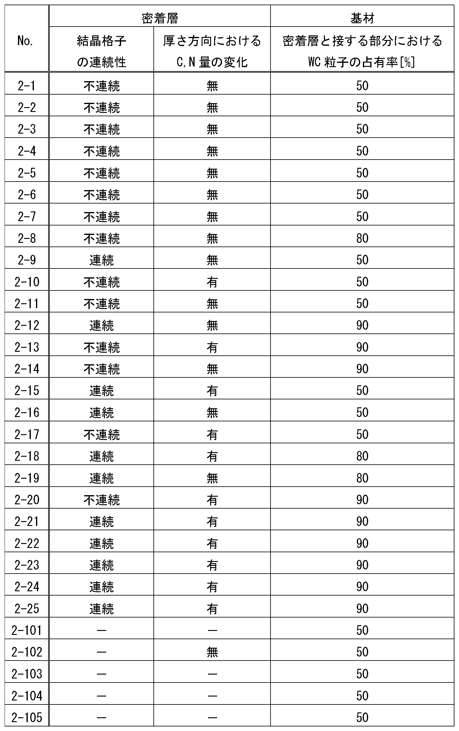
上記で作製した各試料を使用し、乾式の断続切削試験を行って工具寿命を評価した。切削条件は次の通りとし、工具寿命に至るまでの切削距離を測定した。結果を表5に示す。表5中、切削距離が長いほど工具寿命が長いことを示している。
被削材:ステンレス鋼(SUS316)
切削速度:200m/min
送り速度:0.2mm/刃
切り込み量ap:2.0mm
切り込み量ae:50mm
ここで「切り込み量ap」は軸方向の切り込み量を、「切り込み量ae」は半径方向の切り込み量をそれぞれ示している。
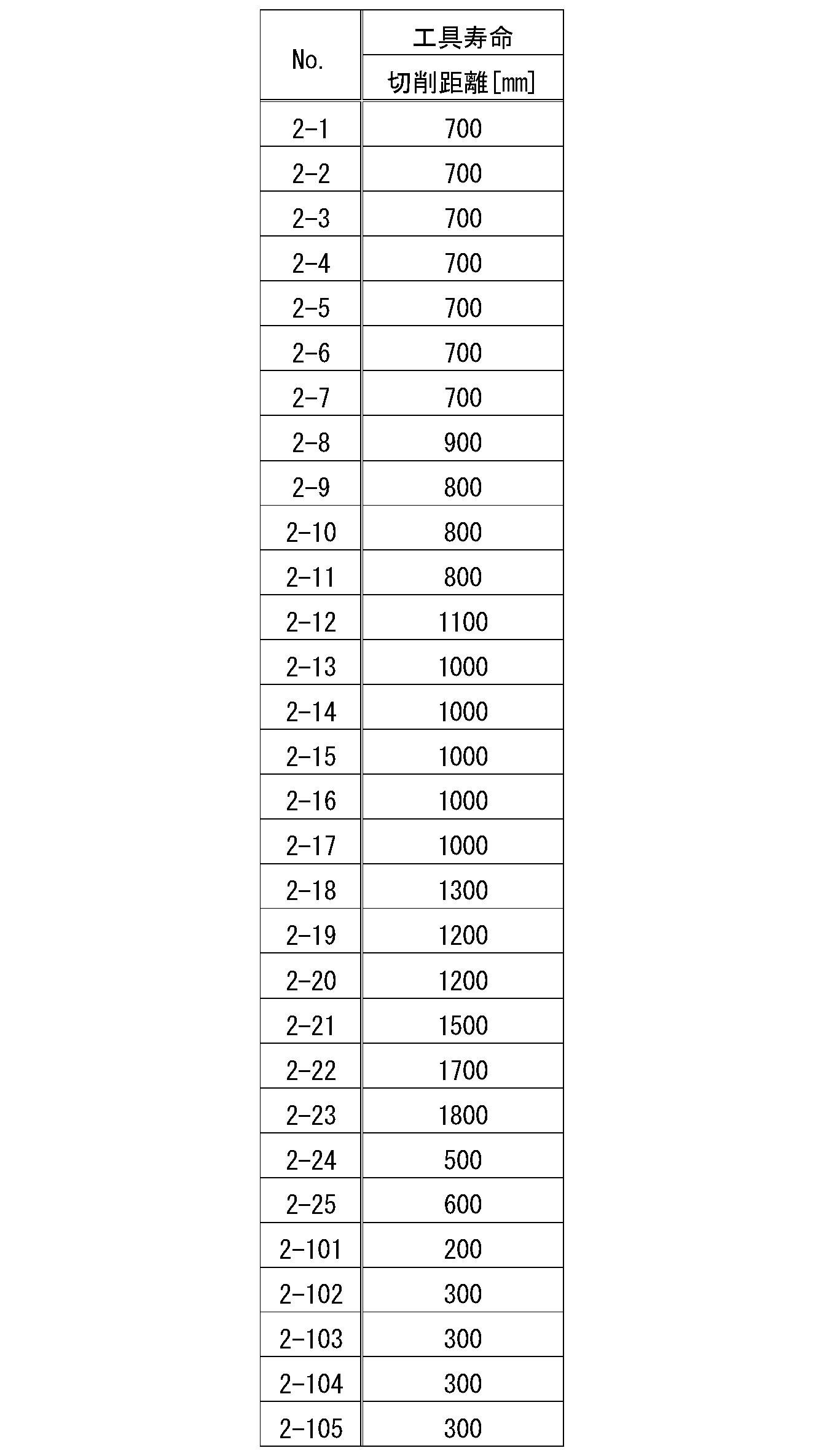
Claims (13)
- 基材と、前記基材上に形成された被膜とを備え、
前記被膜は、A層とB層とが交互にそれぞれ1層以上積層された交互層を含み、
前記A層の厚さおよび前記B層の厚さは、それぞれ2nm以上100nm以下であり、
前記A層の平均組成は、TiaAlbSicN(ただし、0.5<a<0.8、0.2<b<0.4、0.01<c<0.1、a+b+c=1)で表され、
前記B層の平均組成は、TidAleSifN(ただし、0.4<d<0.6、0.3<e<0.7、0.01<f<0.1、d+e+f=1)で表され、
0.05<a-d≦0.2かつ0.05<e-b≦0.2を満たす、表面被覆工具。 - 前記A層の厚さをλAとし、前記B層の厚さをλBとするとき、
1≦λA/λB<5を満たす、請求項1に記載の表面被覆工具。 - 前記被膜は、前記基材と接する部分に密着層をさらに含み、
前記密着層の厚さは、0.5nm以上20nm以下であり、
前記密着層は、
Cr、Ti、ZrおよびNbから選択される1種以上の元素と、
前記基材を構成する元素から選択される1種以上の元素と、
AlおよびSiから選択される1種以上の元素と、を含む炭化物、窒化物もしくは炭窒化物を含有する、請求項1または請求項2に記載の表面被覆工具。 - 前記基材は、WCを含有する硬質粒子と、Coを含有し前記硬質粒子同士を互いに結合する結合相とを含み、
前記密着層は、W、Cr、Ti、AlおよびSiを含む窒化物を含有する、請求項3に記載の表面被覆工具。 - 基材と、前記基材上に形成された被膜とを備え、
前記基材は、WC粒子と、Coを含有し前記WC粒子同士を互いに結合する結合相とを含み、
前記被膜は、前記基材と接する密着層と、前記密着層上に形成された上部層とを含み、
前記密着層の厚さは、0.5nm以上20nm以下であり、
前記密着層は、
Cr、Ti、ZrおよびNbから選択される1種以上の元素と、
前記基材を構成する元素から選択される1種以上の元素と、
前記上部層を構成する元素から選択される1種以上の元素と、を含む炭化物、窒化物もしくは炭窒化物を含有する、表面被覆工具。 - 前記上部層は、周期表の第4族元素、第5族元素および第6族元素ならびにSiおよびAlから選択される1種以上の元素と、C、NおよびOから選択される1種以上の元素とを含む、請求項5に記載の表面被覆工具。
- 前記密着層は、Cr、Ti、ZrおよびNbから選択される1種以上の元素と、Wと、AlおよびSiから選択される1種以上の元素と、を含む炭窒化物を含有する、請求項5または請求項6に記載の表面被覆工具。
- 前記基材のうち前記密着層と接する部分における前記WC粒子の占有率は、80%以上である、請求項5~請求項7のいずれか1項に記載の表面被覆工具。
- 前記被膜の厚さ方向において、
前記密着層に含まれるCの組成比が、前記上部層側から前記基材側に向かって連続的に増加し前記基材との界面で最大となり、
前記密着層に含まれるNの組成比が、前記基材側から前記上部層側に向かって連続的に増加し前記上部層との界面で最大となる、請求項5~請求項8のいずれか1項に記載の表面被覆工具。 - 前記WC粒子の平均粒径は、2μm以下であり、
前記基材におけるCoの含有量は、10質量%以下である、請求項5~請求項9のいずれか1項に記載の表面被覆工具。 - WC粒子と、Coを含有し前記WC粒子同士を互いに結合する結合相とを含む基材を準備する工程と、
前記基材上に被膜を形成する工程と、を備え、
前記被膜を形成する工程は、
前記基材の表面にCr、Ti、ZrおよびNbから選択される1種以上の元素を付着させる工程と、
前記基材上に密着層を形成する工程と、
前記密着層上に上部層を形成する工程と、を含み、
前記密着層の厚さは、0.5nm以上20nm以下であり、
前記密着層を形成する工程は、
前記付着させる工程後の前記表面上に、前記上部層を構成する元素から選択される1種以上の元素を堆積させることにより、Cr、Ti、ZrおよびNbから選択される1種以上の元素と、前記基材を構成する元素から選択される1種以上の元素と、前記上部層を構成する元素から選択される1種以上の元素とを含む炭化物、窒化物もしくは炭窒化物を生成させる工程を含む、表面被覆工具の製造方法。 - 前記付着させる工程は、Cr、Ti、ZrおよびNbから選択される1種以上の元素のイオンを用いたイオンボンバードメント処理によって前記表面を洗浄する工程を含む、請求項11に記載の表面被覆工具の製造方法。
- 前記被膜を形成する工程は、前記付着させる工程の前に、Arイオンを用いたイオンボンバードメント処理によって、前記基材の前記表面に表出した前記結合相の少なくとも一部を除去する工程を、さらに含む、請求項11または請求項12に記載の表面被覆工具の製造方法。
Priority Applications (6)
| Application Number | Priority Date | Filing Date | Title |
|---|---|---|---|
| US14/909,559 US9962771B2 (en) | 2014-06-06 | 2015-05-19 | Surface-coated tool and method of manufacturing the same |
| EP18166619.9A EP3363568B1 (en) | 2014-06-06 | 2015-05-19 | Surface-coated tool and method of manufacturing same |
| KR1020167002527A KR20170016811A (ko) | 2014-06-06 | 2015-05-19 | 표면 피복 공구 및 그 제조 방법 |
| JP2016500420A JP6481983B2 (ja) | 2014-06-06 | 2015-05-19 | 表面被覆工具 |
| CN201580001606.XA CN105473261B (zh) | 2014-06-06 | 2015-05-19 | 表面被覆工具及其制造方法 |
| EP15803152.6A EP3153259B1 (en) | 2014-06-06 | 2015-05-19 | Surface-coated tool and method for manufacturing same |
Applications Claiming Priority (4)
| Application Number | Priority Date | Filing Date | Title |
|---|---|---|---|
| JP2014-117680 | 2014-06-06 | ||
| JP2014117680 | 2014-06-06 | ||
| JP2014-117679 | 2014-06-06 | ||
| JP2014117679 | 2014-06-06 |
Publications (1)
| Publication Number | Publication Date |
|---|---|
| WO2015186503A1 true WO2015186503A1 (ja) | 2015-12-10 |
Family
ID=54766579
Family Applications (1)
| Application Number | Title | Priority Date | Filing Date |
|---|---|---|---|
| PCT/JP2015/064293 Ceased WO2015186503A1 (ja) | 2014-06-06 | 2015-05-19 | 表面被覆工具およびその製造方法 |
Country Status (6)
| Country | Link |
|---|---|
| US (1) | US9962771B2 (ja) |
| EP (2) | EP3153259B1 (ja) |
| JP (2) | JP6481983B2 (ja) |
| KR (1) | KR20170016811A (ja) |
| CN (1) | CN105473261B (ja) |
| WO (1) | WO2015186503A1 (ja) |
Cited By (13)
| Publication number | Priority date | Publication date | Assignee | Title |
|---|---|---|---|---|
| CN106319449A (zh) * | 2016-10-25 | 2017-01-11 | 郑州航空工业管理学院 | 用于航空涡喷发动机压气机叶片的防冲蚀梯度膜及其制备方法 |
| WO2017169498A1 (ja) * | 2016-03-28 | 2017-10-05 | 住友電工ハードメタル株式会社 | 表面被覆切削工具、およびその製造方法 |
| WO2017183327A1 (ja) * | 2016-04-19 | 2017-10-26 | 住友電工ハードメタル株式会社 | 表面被覆切削工具 |
| JP2020520814A (ja) * | 2017-05-19 | 2020-07-16 | ヴァルター アーゲー | 多層コーティングを有する金属切削ツール |
| JP2020124748A (ja) * | 2019-02-01 | 2020-08-20 | 京セラ株式会社 | 被覆工具及びこれを備えた切削工具 |
| WO2020166466A1 (ja) * | 2019-02-12 | 2020-08-20 | 三菱マテリアル株式会社 | 硬質皮膜切削工具 |
| JPWO2020184352A1 (ja) * | 2019-03-14 | 2020-09-17 | ||
| US10994339B2 (en) | 2016-12-09 | 2021-05-04 | Sumitomo Electric Hardmetal Corp. | Surface-coated cutting tool |
| CN113652639A (zh) * | 2021-08-24 | 2021-11-16 | 株洲索尔切削工具有限公司 | 梯度结构的合金涂层及其制备方法 |
| CN114173974A (zh) * | 2019-10-10 | 2022-03-11 | 住友电工硬质合金株式会社 | 切削工具 |
| JP2023048174A (ja) * | 2021-09-28 | 2023-04-07 | 三菱マテリアル株式会社 | 表面被覆切削工具 |
| JP2023086393A (ja) * | 2021-12-10 | 2023-06-22 | 株式会社タンガロイ | 被覆切削工具 |
| WO2023182126A1 (ja) * | 2022-03-22 | 2023-09-28 | 三菱マテリアル株式会社 | 表面被覆切削工具 |
Families Citing this family (22)
| Publication number | Priority date | Publication date | Assignee | Title |
|---|---|---|---|---|
| EP3228726A1 (en) * | 2016-04-08 | 2017-10-11 | Seco Tools Ab | Coated cutting tool |
| JP6699056B2 (ja) * | 2016-06-14 | 2020-05-27 | 住友電工ハードメタル株式会社 | 表面被覆切削工具 |
| DE102016222296A1 (de) * | 2016-11-14 | 2018-05-17 | Siemens Aktiengesellschaft | Mehrlagige aluminiumhaltige Schutzbeschichtung und Bauteil |
| US11192189B2 (en) * | 2017-05-30 | 2021-12-07 | Kyocera Corporation | Coated tool and cutting tool including same |
| US10570501B2 (en) | 2017-05-31 | 2020-02-25 | Kennametal Inc. | Multilayer nitride hard coatings |
| CN110769956B (zh) * | 2017-06-20 | 2021-02-26 | 京瓷株式会社 | 涂层刀具、切削工具以及切削加工物的制造方法 |
| JP6858347B2 (ja) * | 2017-07-28 | 2021-04-14 | 株式会社タンガロイ | 被覆切削工具 |
| RU2691811C2 (ru) * | 2017-11-14 | 2019-06-18 | федеральное государственное бюджетное образовательное учреждение высшего образования "Ульяновский государственный технический университет" | Способ получения износостойкого покрытия для режущего инструмента |
| CN112368094B (zh) * | 2018-06-15 | 2023-07-21 | 住友电工硬质合金株式会社 | 表面被覆切削工具及其制造方法 |
| CN110079766A (zh) * | 2019-05-27 | 2019-08-02 | 国宏工具系统(无锡)股份有限公司 | 一种高效加工高温合金纳米复合涂层工艺 |
| CN110578122A (zh) * | 2019-10-18 | 2019-12-17 | 天津职业技术师范大学(中国职业培训指导教师进修中心) | 一种AlTiN/AlTiSiN多层纳米复合涂层的制备工艺 |
| CN114929415B (zh) * | 2020-01-08 | 2024-10-18 | 住友电工硬质合金株式会社 | 切削工具 |
| CN112111747B (zh) * | 2020-08-24 | 2024-03-01 | 青岛理工大学 | 一种硬质合金刀具清洗、涂层生产线及方法 |
| EP4144465B1 (en) * | 2020-12-16 | 2024-04-10 | Sumitomo Electric Hardmetal Corp. | Coated cutting tool with a layer made of tungsten metal and hexagonal di-tungsten carbide |
| DE112022003746T5 (de) * | 2021-07-30 | 2024-05-29 | Kyocera Corporation | Beschichtetes werkzeug und schneidwerkzeug |
| CN117561134A (zh) * | 2021-07-30 | 2024-02-13 | 京瓷株式会社 | 涂层刀具及切削刀具 |
| US20250163564A1 (en) | 2022-02-28 | 2025-05-22 | Kyocera Corporation | Coated tool and cutting tool |
| JP2025518128A (ja) * | 2022-06-01 | 2025-06-12 | エービー サンドビック コロマント | 被覆切削工具 |
| EP4667143A1 (en) | 2023-02-13 | 2025-12-24 | Mitsubishi Materials Corporation | Surface-coated cutting tool |
| WO2024180128A1 (en) * | 2023-02-28 | 2024-09-06 | Ab Sandvik Coromant | A coated cutting tool |
| JP2025017171A (ja) * | 2023-07-24 | 2025-02-05 | 株式会社Moldino | 被覆切削工具 |
| WO2025181307A1 (en) * | 2024-02-28 | 2025-09-04 | Ab Sandvik Coromant | A coated cutting tool |
Citations (4)
| Publication number | Priority date | Publication date | Assignee | Title |
|---|---|---|---|---|
| JP2004223619A (ja) * | 2003-01-20 | 2004-08-12 | Mitsubishi Materials Kobe Tools Corp | 高速重切削条件で硬質被覆層がすぐれた耐摩耗性を発揮する表面被覆超硬合金製切削工具 |
| JP2007002332A (ja) * | 2005-05-26 | 2007-01-11 | Hitachi Tool Engineering Ltd | 硬質皮膜被覆部材 |
| JP2010018861A (ja) * | 2008-07-11 | 2010-01-28 | Toyota Central R&D Labs Inc | 被覆超硬合金部材 |
| JP5109199B2 (ja) * | 2007-09-11 | 2012-12-26 | 住友電工ハードメタル株式会社 | 表面被覆切削工具 |
Family Cites Families (32)
| Publication number | Priority date | Publication date | Assignee | Title |
|---|---|---|---|---|
| US4101703A (en) * | 1972-02-04 | 1978-07-18 | Schwarzkopf Development Corporation | Coated cemented carbide elements |
| CH632944A5 (fr) * | 1978-06-22 | 1982-11-15 | Stellram Sa | Piece d'usure en metal dur. |
| JPH05109199A (ja) * | 1991-10-18 | 1993-04-30 | Mita Ind Co Ltd | 磁気テープ記録装置 |
| JP3044910B2 (ja) * | 1992-03-24 | 2000-05-22 | 三菱マテリアル株式会社 | 物理蒸着硬質層被覆エンドミルおよびその製造法 |
| JP2793773B2 (ja) | 1994-05-13 | 1998-09-03 | 神鋼コベルコツール株式会社 | 耐摩耗性に優れた硬質皮膜、硬質皮膜被覆工具及び硬質皮膜被覆部材 |
| JP3416937B2 (ja) | 1994-10-28 | 2003-06-16 | 住友電気工業株式会社 | 積層体 |
| SE509566C2 (sv) * | 1996-07-11 | 1999-02-08 | Sandvik Ab | Sintringsmetod |
| WO1998002395A1 (en) * | 1996-07-11 | 1998-01-22 | Sandvik Ab (Publ) | Sintering method |
| SE9903089D0 (sv) * | 1999-09-01 | 1999-09-01 | Sandvik Ab | Coated grooving or parting insert |
| SE9903122D0 (sv) * | 1999-09-06 | 1999-09-06 | Sandvik Ab | Coated cemented carbide insert |
| JP4535250B2 (ja) * | 2004-07-08 | 2010-09-01 | 三菱マテリアル株式会社 | 高硬度鋼の高速切削加工で硬質被覆層がすぐれた耐摩耗性を発揮する表面被覆超硬合金製切削工具の製造方法 |
| JP2006028600A (ja) * | 2004-07-16 | 2006-02-02 | Kobe Steel Ltd | 耐摩耗性と耐熱性に優れた積層皮膜 |
| JP2006070730A (ja) | 2004-08-31 | 2006-03-16 | Mazda Motor Corp | エンジンの制御装置 |
| WO2006070509A1 (ja) | 2004-12-28 | 2006-07-06 | Sumitomo Electric Hardmetal Corp. | 表面被覆切削工具および表面被覆切削工具の製造方法 |
| WO2006070730A1 (ja) | 2004-12-28 | 2006-07-06 | Sumitomo Electric Hardmetal Corp. | 表面被覆切削工具および表面被覆切削工具の製造方法 |
| JP4702520B2 (ja) * | 2005-02-14 | 2011-06-15 | 三菱マテリアル株式会社 | 高硬度鋼の高速切削加工で硬質被覆層がすぐれた耐摩耗性を発揮する表面被覆超硬合金製切削工具 |
| GB2425780B (en) * | 2005-04-27 | 2007-09-05 | Univ Sheffield Hallam | PVD coated substrate |
| US7537822B2 (en) | 2005-05-26 | 2009-05-26 | Hitachi Tool Engineering, Ltd. | Hard-coated member |
| JP4716006B2 (ja) * | 2005-07-08 | 2011-07-06 | 三菱マテリアル株式会社 | 合金鋼の高速歯切加工で硬質被覆層がすぐれた耐摩耗性を発揮する表面被覆高速度工具鋼製歯切工具 |
| JP4815925B2 (ja) | 2005-07-27 | 2011-11-16 | 株式会社タンガロイ | 被覆焼結合金 |
| JP4702535B2 (ja) * | 2005-09-21 | 2011-06-15 | 三菱マテリアル株式会社 | 高硬度鋼の高速切削加工で硬質被覆層がすぐれた耐摩耗性を発揮する表面被覆高速度工具鋼製切削工具 |
| JP4702538B2 (ja) * | 2005-10-14 | 2011-06-15 | 三菱マテリアル株式会社 | 高硬度鋼の高速切削加工で硬質被覆層がすぐれた耐摩耗性を発揮する表面被覆切削工具 |
| SE529838C2 (sv) * | 2005-12-08 | 2007-12-04 | Sandvik Intellectual Property | Belagt hårdmetallskär, sätt att framställa detta samt dess användning för fräsning i stål |
| JP2007290090A (ja) * | 2006-04-26 | 2007-11-08 | Mitsubishi Materials Corp | 難削材の高速重切削加工で硬質被覆層がすぐれた耐チッピング性を発揮する表面被覆切削工具 |
| SE0602814L (sv) * | 2006-12-27 | 2008-06-28 | Sandvik Intellectual Property | Skärverktyg med multiskiktbeläggning |
| SE0701760L (sv) * | 2007-06-01 | 2008-12-02 | Sandvik Intellectual Property | Hårdmetallskär för avstickning, spårstickning och gängning |
| GB2450933A (en) * | 2007-07-13 | 2009-01-14 | Hauzer Techno Coating Bv | Method of providing a hard coating |
| JP5098726B2 (ja) * | 2008-02-22 | 2012-12-12 | 日立ツール株式会社 | 被覆工具及び被覆工具の製造方法 |
| JP5594576B2 (ja) * | 2010-04-20 | 2014-09-24 | 三菱マテリアル株式会社 | 硬質被覆層がすぐれた耐摩耗性を発揮する表面被覆切削工具 |
| CN103717331B (zh) * | 2011-08-01 | 2016-03-02 | 日立工具股份有限公司 | 表面改性wc基超硬合金部件、硬质皮膜被覆wc基超硬合金部件以及它们的制造方法 |
| US8691374B2 (en) | 2011-09-14 | 2014-04-08 | Kennametal Inc. | Multilayer coated wear-resistant member and method for making the same |
| JP6331003B2 (ja) * | 2013-11-07 | 2018-05-30 | 三菱マテリアル株式会社 | 表面被覆切削工具 |
-
2015
- 2015-05-19 KR KR1020167002527A patent/KR20170016811A/ko not_active Abandoned
- 2015-05-19 EP EP15803152.6A patent/EP3153259B1/en active Active
- 2015-05-19 US US14/909,559 patent/US9962771B2/en active Active
- 2015-05-19 EP EP18166619.9A patent/EP3363568B1/en active Active
- 2015-05-19 JP JP2016500420A patent/JP6481983B2/ja active Active
- 2015-05-19 WO PCT/JP2015/064293 patent/WO2015186503A1/ja not_active Ceased
- 2015-05-19 CN CN201580001606.XA patent/CN105473261B/zh active Active
-
2018
- 2018-12-18 JP JP2018236438A patent/JP6773287B2/ja active Active
Patent Citations (4)
| Publication number | Priority date | Publication date | Assignee | Title |
|---|---|---|---|---|
| JP2004223619A (ja) * | 2003-01-20 | 2004-08-12 | Mitsubishi Materials Kobe Tools Corp | 高速重切削条件で硬質被覆層がすぐれた耐摩耗性を発揮する表面被覆超硬合金製切削工具 |
| JP2007002332A (ja) * | 2005-05-26 | 2007-01-11 | Hitachi Tool Engineering Ltd | 硬質皮膜被覆部材 |
| JP5109199B2 (ja) * | 2007-09-11 | 2012-12-26 | 住友電工ハードメタル株式会社 | 表面被覆切削工具 |
| JP2010018861A (ja) * | 2008-07-11 | 2010-01-28 | Toyota Central R&D Labs Inc | 被覆超硬合金部材 |
Cited By (31)
| Publication number | Priority date | Publication date | Assignee | Title |
|---|---|---|---|---|
| US11872636B2 (en) | 2016-03-28 | 2024-01-16 | Sumitomo Electric Hardmetal Corp. | Surface-coated cutting tool and method for manufacturing same |
| WO2017169498A1 (ja) * | 2016-03-28 | 2017-10-05 | 住友電工ハードメタル株式会社 | 表面被覆切削工具、およびその製造方法 |
| JP2017177239A (ja) * | 2016-03-28 | 2017-10-05 | 住友電工ハードメタル株式会社 | 表面被覆切削工具、およびその製造方法 |
| WO2017183327A1 (ja) * | 2016-04-19 | 2017-10-26 | 住友電工ハードメタル株式会社 | 表面被覆切削工具 |
| JP2017193004A (ja) * | 2016-04-19 | 2017-10-26 | 住友電工ハードメタル株式会社 | 表面被覆切削工具 |
| CN109070235A (zh) * | 2016-04-19 | 2018-12-21 | 住友电工硬质合金株式会社 | 表面被覆切削工具 |
| EP3446814A4 (en) * | 2016-04-19 | 2019-11-27 | Sumitomo Electric Hardmetal Corp. | SURFACE-FINISHED CUTTING TOOL |
| US11167357B2 (en) | 2016-04-19 | 2021-11-09 | Sumitomo Electric Hardmetal Corp. | Surface-coated cutting tool |
| CN106319449A (zh) * | 2016-10-25 | 2017-01-11 | 郑州航空工业管理学院 | 用于航空涡喷发动机压气机叶片的防冲蚀梯度膜及其制备方法 |
| US10994339B2 (en) | 2016-12-09 | 2021-05-04 | Sumitomo Electric Hardmetal Corp. | Surface-coated cutting tool |
| JP7299164B2 (ja) | 2017-05-19 | 2023-06-27 | ヴァルター アーゲー | 多層コーティングを有する金属切削ツール |
| JP2020520814A (ja) * | 2017-05-19 | 2020-07-16 | ヴァルター アーゲー | 多層コーティングを有する金属切削ツール |
| JP2020124748A (ja) * | 2019-02-01 | 2020-08-20 | 京セラ株式会社 | 被覆工具及びこれを備えた切削工具 |
| JP7211656B2 (ja) | 2019-02-01 | 2023-01-24 | 京セラ株式会社 | 被覆工具及びこれを備えた切削工具 |
| WO2020166466A1 (ja) * | 2019-02-12 | 2020-08-20 | 三菱マテリアル株式会社 | 硬質皮膜切削工具 |
| JP7733444B2 (ja) | 2019-02-12 | 2025-09-03 | 三菱マテリアル株式会社 | 硬質皮膜切削工具 |
| US12303982B2 (en) | 2019-02-12 | 2025-05-20 | Mitsubishi Materials Corporation | Surface-coated cutting tool |
| JPWO2020184352A1 (ja) * | 2019-03-14 | 2020-09-17 | ||
| WO2020184352A1 (ja) * | 2019-03-14 | 2020-09-17 | 三菱マテリアル株式会社 | 表面被覆切削工具 |
| JP7492683B2 (ja) | 2019-03-14 | 2024-05-30 | 三菱マテリアル株式会社 | 表面被覆切削工具 |
| CN114173974A (zh) * | 2019-10-10 | 2022-03-11 | 住友电工硬质合金株式会社 | 切削工具 |
| CN114173974B (zh) * | 2019-10-10 | 2024-03-15 | 住友电工硬质合金株式会社 | 切削工具 |
| CN113652639A (zh) * | 2021-08-24 | 2021-11-16 | 株洲索尔切削工具有限公司 | 梯度结构的合金涂层及其制备方法 |
| JP7709118B2 (ja) | 2021-09-28 | 2025-07-16 | 三菱マテリアル株式会社 | 表面被覆切削工具 |
| JP2023048174A (ja) * | 2021-09-28 | 2023-04-07 | 三菱マテリアル株式会社 | 表面被覆切削工具 |
| JP7319600B6 (ja) | 2021-12-10 | 2023-08-18 | 株式会社タンガロイ | 被覆切削工具 |
| JP7319600B2 (ja) | 2021-12-10 | 2023-08-02 | 株式会社タンガロイ | 被覆切削工具 |
| JP2023086393A (ja) * | 2021-12-10 | 2023-06-22 | 株式会社タンガロイ | 被覆切削工具 |
| JPWO2023182126A1 (ja) * | 2022-03-22 | 2023-09-28 | ||
| WO2023182126A1 (ja) * | 2022-03-22 | 2023-09-28 | 三菱マテリアル株式会社 | 表面被覆切削工具 |
| JP7794294B2 (ja) | 2022-03-22 | 2026-01-06 | 三菱マテリアル株式会社 | 表面被覆切削工具 |
Also Published As
| Publication number | Publication date |
|---|---|
| US20160175939A1 (en) | 2016-06-23 |
| EP3153259A1 (en) | 2017-04-12 |
| CN105473261A (zh) | 2016-04-06 |
| JPWO2015186503A1 (ja) | 2017-04-20 |
| EP3363568B1 (en) | 2023-08-30 |
| EP3153259A4 (en) | 2018-01-24 |
| EP3363568A1 (en) | 2018-08-22 |
| JP2019069514A (ja) | 2019-05-09 |
| JP6481983B2 (ja) | 2019-03-13 |
| CN105473261B (zh) | 2017-08-18 |
| US9962771B2 (en) | 2018-05-08 |
| KR20170016811A (ko) | 2017-02-14 |
| EP3153259B1 (en) | 2020-05-06 |
| JP6773287B2 (ja) | 2020-10-21 |
Similar Documents
| Publication | Publication Date | Title |
|---|---|---|
| JP6481983B2 (ja) | 表面被覆工具 | |
| US11872636B2 (en) | Surface-coated cutting tool and method for manufacturing same | |
| KR102198744B1 (ko) | 표면 피복 절삭 공구 | |
| JP5542925B2 (ja) | 切削工具 | |
| JP5838769B2 (ja) | 表面被覆切削工具 | |
| JP2006152321A (ja) | 硬質皮膜被覆部材及びその被覆方法 | |
| JP5488824B2 (ja) | 硬質難削材の高速切削加工で硬質被覆層がすぐれた耐剥離性とすぐれた耐摩耗性を発揮する表面被覆切削工具 | |
| JP6331003B2 (ja) | 表面被覆切削工具 | |
| CN112368094A (zh) | 表面被覆切削工具及其制造方法 | |
| WO2016084939A1 (ja) | 耐チッピング性、耐摩耗性にすぐれた表面被覆切削工具 | |
| JP2012139795A (ja) | 軟質難削材の高速切削加工で硬質被覆層がすぐれた耐剥離性とすぐれた耐チッピング性を発揮する表面被覆切削工具 | |
| JP5553013B2 (ja) | 硬質難削材の高速高送り切削加工で硬質被覆層がすぐれた耐剥離性とすぐれた耐チッピング性を発揮する表面被覆切削工具 | |
| JP6233588B2 (ja) | 表面被覆切削工具 | |
| JP2019171483A (ja) | 表面被覆切削工具 | |
| JP2012115967A (ja) | 硬質難削材の断続切削加工で硬質被覆層がすぐれた耐剥離性とすぐれた耐チッピング性を発揮する表面被覆切削工具 | |
| JP2009178832A (ja) | 硬質被覆層がすぐれた潤滑性と耐摩耗性を発揮する表面被覆切削工具 |
Legal Events
| Date | Code | Title | Description |
|---|---|---|---|
| WWE | Wipo information: entry into national phase |
Ref document number: 201580001606.X Country of ref document: CN |
|
| ENP | Entry into the national phase |
Ref document number: 2016500420 Country of ref document: JP Kind code of ref document: A |
|
| 121 | Ep: the epo has been informed by wipo that ep was designated in this application |
Ref document number: 15803152 Country of ref document: EP Kind code of ref document: A1 |
|
| ENP | Entry into the national phase |
Ref document number: 20167002527 Country of ref document: KR Kind code of ref document: A |
|
| REEP | Request for entry into the european phase |
Ref document number: 2015803152 Country of ref document: EP |
|
| WWE | Wipo information: entry into national phase |
Ref document number: 2015803152 Country of ref document: EP |
|
| WWE | Wipo information: entry into national phase |
Ref document number: 14909559 Country of ref document: US |
|
| NENP | Non-entry into the national phase |
Ref country code: DE |