WO2015159800A1 - 液晶表示パネルおよびその製造方法 - Google Patents
液晶表示パネルおよびその製造方法 Download PDFInfo
- Publication number
- WO2015159800A1 WO2015159800A1 PCT/JP2015/061125 JP2015061125W WO2015159800A1 WO 2015159800 A1 WO2015159800 A1 WO 2015159800A1 JP 2015061125 W JP2015061125 W JP 2015061125W WO 2015159800 A1 WO2015159800 A1 WO 2015159800A1
- Authority
- WO
- WIPO (PCT)
- Prior art keywords
- layer
- liquid crystal
- insulating layer
- interlayer insulating
- organic interlayer
- Prior art date
- Legal status (The legal status is an assumption and is not a legal conclusion. Google has not performed a legal analysis and makes no representation as to the accuracy of the status listed.)
- Ceased
Links
Images

Classifications
-
- G—PHYSICS
- G02—OPTICS
- G02F—OPTICAL DEVICES OR ARRANGEMENTS FOR THE CONTROL OF LIGHT BY MODIFICATION OF THE OPTICAL PROPERTIES OF THE MEDIA OF THE ELEMENTS INVOLVED THEREIN; NON-LINEAR OPTICS; FREQUENCY-CHANGING OF LIGHT; OPTICAL LOGIC ELEMENTS; OPTICAL ANALOGUE/DIGITAL CONVERTERS
- G02F1/00—Devices or arrangements for the control of the intensity, colour, phase, polarisation or direction of light arriving from an independent light source, e.g. switching, gating or modulating; Non-linear optics
- G02F1/01—Devices or arrangements for the control of the intensity, colour, phase, polarisation or direction of light arriving from an independent light source, e.g. switching, gating or modulating; Non-linear optics for the control of the intensity, phase, polarisation or colour
- G02F1/13—Devices or arrangements for the control of the intensity, colour, phase, polarisation or direction of light arriving from an independent light source, e.g. switching, gating or modulating; Non-linear optics for the control of the intensity, phase, polarisation or colour based on liquid crystals, e.g. single liquid crystal display cells
- G02F1/133—Constructional arrangements; Operation of liquid crystal cells; Circuit arrangements
- G02F1/136—Liquid crystal cells structurally associated with a semi-conducting layer or substrate, e.g. cells forming part of an integrated circuit
- G02F1/1362—Active matrix addressed cells
- G02F1/136227—Through-hole connection of the pixel electrode to the active element through an insulation layer
-
- G—PHYSICS
- G02—OPTICS
- G02F—OPTICAL DEVICES OR ARRANGEMENTS FOR THE CONTROL OF LIGHT BY MODIFICATION OF THE OPTICAL PROPERTIES OF THE MEDIA OF THE ELEMENTS INVOLVED THEREIN; NON-LINEAR OPTICS; FREQUENCY-CHANGING OF LIGHT; OPTICAL LOGIC ELEMENTS; OPTICAL ANALOGUE/DIGITAL CONVERTERS
- G02F1/00—Devices or arrangements for the control of the intensity, colour, phase, polarisation or direction of light arriving from an independent light source, e.g. switching, gating or modulating; Non-linear optics
- G02F1/01—Devices or arrangements for the control of the intensity, colour, phase, polarisation or direction of light arriving from an independent light source, e.g. switching, gating or modulating; Non-linear optics for the control of the intensity, phase, polarisation or colour
- G02F1/13—Devices or arrangements for the control of the intensity, colour, phase, polarisation or direction of light arriving from an independent light source, e.g. switching, gating or modulating; Non-linear optics for the control of the intensity, phase, polarisation or colour based on liquid crystals, e.g. single liquid crystal display cells
- G02F1/133—Constructional arrangements; Operation of liquid crystal cells; Circuit arrangements
- G02F1/1333—Constructional arrangements; Manufacturing methods
- G02F1/133345—Insulating layers
-
- G—PHYSICS
- G02—OPTICS
- G02F—OPTICAL DEVICES OR ARRANGEMENTS FOR THE CONTROL OF LIGHT BY MODIFICATION OF THE OPTICAL PROPERTIES OF THE MEDIA OF THE ELEMENTS INVOLVED THEREIN; NON-LINEAR OPTICS; FREQUENCY-CHANGING OF LIGHT; OPTICAL LOGIC ELEMENTS; OPTICAL ANALOGUE/DIGITAL CONVERTERS
- G02F1/00—Devices or arrangements for the control of the intensity, colour, phase, polarisation or direction of light arriving from an independent light source, e.g. switching, gating or modulating; Non-linear optics
- G02F1/01—Devices or arrangements for the control of the intensity, colour, phase, polarisation or direction of light arriving from an independent light source, e.g. switching, gating or modulating; Non-linear optics for the control of the intensity, phase, polarisation or colour
- G02F1/13—Devices or arrangements for the control of the intensity, colour, phase, polarisation or direction of light arriving from an independent light source, e.g. switching, gating or modulating; Non-linear optics for the control of the intensity, phase, polarisation or colour based on liquid crystals, e.g. single liquid crystal display cells
- G02F1/133—Constructional arrangements; Operation of liquid crystal cells; Circuit arrangements
- G02F1/1333—Constructional arrangements; Manufacturing methods
- G02F1/1343—Electrodes
- G02F1/134309—Electrodes characterised by their geometrical arrangement
- G02F1/134363—Electrodes characterised by their geometrical arrangement for applying an electric field parallel to the substrate, i.e. in-plane switching [IPS]
-
- G—PHYSICS
- G02—OPTICS
- G02F—OPTICAL DEVICES OR ARRANGEMENTS FOR THE CONTROL OF LIGHT BY MODIFICATION OF THE OPTICAL PROPERTIES OF THE MEDIA OF THE ELEMENTS INVOLVED THEREIN; NON-LINEAR OPTICS; FREQUENCY-CHANGING OF LIGHT; OPTICAL LOGIC ELEMENTS; OPTICAL ANALOGUE/DIGITAL CONVERTERS
- G02F1/00—Devices or arrangements for the control of the intensity, colour, phase, polarisation or direction of light arriving from an independent light source, e.g. switching, gating or modulating; Non-linear optics
- G02F1/01—Devices or arrangements for the control of the intensity, colour, phase, polarisation or direction of light arriving from an independent light source, e.g. switching, gating or modulating; Non-linear optics for the control of the intensity, phase, polarisation or colour
- G02F1/13—Devices or arrangements for the control of the intensity, colour, phase, polarisation or direction of light arriving from an independent light source, e.g. switching, gating or modulating; Non-linear optics for the control of the intensity, phase, polarisation or colour based on liquid crystals, e.g. single liquid crystal display cells
- G02F1/133—Constructional arrangements; Operation of liquid crystal cells; Circuit arrangements
- G02F1/1333—Constructional arrangements; Manufacturing methods
- G02F1/1343—Electrodes
- G02F1/13439—Electrodes characterised by their electrical, optical, physical properties; materials therefor; method of making
-
- G—PHYSICS
- G02—OPTICS
- G02F—OPTICAL DEVICES OR ARRANGEMENTS FOR THE CONTROL OF LIGHT BY MODIFICATION OF THE OPTICAL PROPERTIES OF THE MEDIA OF THE ELEMENTS INVOLVED THEREIN; NON-LINEAR OPTICS; FREQUENCY-CHANGING OF LIGHT; OPTICAL LOGIC ELEMENTS; OPTICAL ANALOGUE/DIGITAL CONVERTERS
- G02F1/00—Devices or arrangements for the control of the intensity, colour, phase, polarisation or direction of light arriving from an independent light source, e.g. switching, gating or modulating; Non-linear optics
- G02F1/01—Devices or arrangements for the control of the intensity, colour, phase, polarisation or direction of light arriving from an independent light source, e.g. switching, gating or modulating; Non-linear optics for the control of the intensity, phase, polarisation or colour
- G02F1/13—Devices or arrangements for the control of the intensity, colour, phase, polarisation or direction of light arriving from an independent light source, e.g. switching, gating or modulating; Non-linear optics for the control of the intensity, phase, polarisation or colour based on liquid crystals, e.g. single liquid crystal display cells
- G02F1/133—Constructional arrangements; Operation of liquid crystal cells; Circuit arrangements
- G02F1/136—Liquid crystal cells structurally associated with a semi-conducting layer or substrate, e.g. cells forming part of an integrated circuit
- G02F1/1362—Active matrix addressed cells
-
- G—PHYSICS
- G02—OPTICS
- G02F—OPTICAL DEVICES OR ARRANGEMENTS FOR THE CONTROL OF LIGHT BY MODIFICATION OF THE OPTICAL PROPERTIES OF THE MEDIA OF THE ELEMENTS INVOLVED THEREIN; NON-LINEAR OPTICS; FREQUENCY-CHANGING OF LIGHT; OPTICAL LOGIC ELEMENTS; OPTICAL ANALOGUE/DIGITAL CONVERTERS
- G02F1/00—Devices or arrangements for the control of the intensity, colour, phase, polarisation or direction of light arriving from an independent light source, e.g. switching, gating or modulating; Non-linear optics
- G02F1/01—Devices or arrangements for the control of the intensity, colour, phase, polarisation or direction of light arriving from an independent light source, e.g. switching, gating or modulating; Non-linear optics for the control of the intensity, phase, polarisation or colour
- G02F1/13—Devices or arrangements for the control of the intensity, colour, phase, polarisation or direction of light arriving from an independent light source, e.g. switching, gating or modulating; Non-linear optics for the control of the intensity, phase, polarisation or colour based on liquid crystals, e.g. single liquid crystal display cells
- G02F1/133—Constructional arrangements; Operation of liquid crystal cells; Circuit arrangements
- G02F1/136—Liquid crystal cells structurally associated with a semi-conducting layer or substrate, e.g. cells forming part of an integrated circuit
- G02F1/1362—Active matrix addressed cells
- G02F1/1368—Active matrix addressed cells in which the switching element is a three-electrode device
Definitions
- the present invention relates to a liquid crystal display panel and a manufacturing method thereof.
- an organic interlayer insulating layer is formed on a thin film transistor (hereinafter referred to as TFT), a gate bus line and a source bus line, and a pixel electrode is formed on the organic interlayer insulating layer.
- TFT thin film transistor
- a gate bus line and a source bus line a gate bus line and a source bus line
- a pixel electrode is formed on the organic interlayer insulating layer.
- Liquid crystal display panels are known (for example, Patent Documents 1 and 2).
- IPS mode transverse electric field mode
- VA mode vertical alignment mode
- FFS mode fringe field switching mode
- a first transparent conductive layer, an inorganic dielectric layer formed on the first transparent conductive layer, and a second transparent conductive layer formed on the inorganic dielectric layer are formed on the organic interlayer insulating layer.
- a liquid crystal display panel comprising:
- the second transparent conductive layer is, for example, a pixel electrode having a plurality of straight portions extending in parallel with each other.
- the second transparent conductive layer typically has a plurality of slits.
- the first transparent conductive layer is, for example, a solid common electrode (sometimes referred to as a “counter electrode”) having no opening such as a slit.
- the first transparent conductive layer, the inorganic dielectric layer, and the second transparent conductive layer form an auxiliary capacitor.
- the inventor has a laminated structure of the above-mentioned second transparent conductive layer / inorganic dielectric layer / first transparent conductive layer / organic interlayer insulating layer (this notation is the second transparent conductive layer is the uppermost layer, and the lower side in the order of description.
- a liquid crystal display panel having an organic interlayer insulating layer as the lowermost layer) was produced.
- the liquid crystal display panel was used for a long time, there was a problem that bubbles were generated in the liquid crystal layer. It was. According to the study of the present inventor, this problem is a new problem caused by forming an inorganic dielectric layer on an organic interlayer insulating layer as will be described later.
- the present invention has been made in order to solve the above-described problems, and has been made to suppress the generation of bubbles in a liquid crystal display panel having an inorganic dielectric layer on an organic interlayer insulating layer.
- a liquid crystal display panel includes a liquid crystal layer, first and second substrates disposed so as to face each other with the liquid crystal layer interposed therebetween, a thin film transistor supported by the first substrate, and the thin film transistor
- An organic interlayer insulating layer covering the organic interlayer insulating layer, a first transparent conductive layer formed in a first region of the surface of the organic interlayer insulating layer, and covering the first transparent conductive layer and of the surface of the organic interlayer insulating layer
- An inorganic dielectric layer containing SiN formed in a second region different from the first region, and the arithmetic average roughness Ra of the first region and the second region of the surface of the organic interlayer insulating layer is 3.45 nm or more and 5.20 nm or less.
- the arithmetic average roughness Ra of the surface of the first transparent conductive layer is 3.75 nm or more and 6.30 nm or less.
- the liquid crystal display panel has a second transparent conductive layer on the inorganic dielectric layer.
- the second transparent conductive layer includes a drain electrode of the thin film transistor in a contact hole including a first contact hole included in the organic interlayer insulating layer and a second contact hole included in the inorganic dielectric layer.
- the inner peripheral surface of the first contact hole is covered with the inorganic dielectric layer.
- the second transparent conductive layer includes a drain electrode of the thin film transistor in a contact hole including a first contact hole included in the organic interlayer insulating layer and a second contact hole included in the inorganic dielectric layer.
- the first contact hole and the second contact hole intersect each other when viewed from the normal direction of the first substrate.
- a method of manufacturing a liquid crystal display panel is a method of manufacturing a liquid crystal display panel having a liquid crystal layer and first and second substrates arranged to face each other with the liquid crystal layer interposed therebetween.
- the ashing is performed in a gas atmosphere containing oxygen.
- a liquid crystal display panel in which the generation of bubbles in the liquid crystal layer is suppressed and a method for manufacturing such a liquid crystal display panel are provided.
- FIG. 1C is a schematic cross-sectional view taken along the line 1B-1B ′ in FIG. 1
- FIG. 3C is a schematic cross-sectional view taken along the line 1C-1C ′ in FIG.
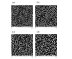
- A)-(d) is a figure which shows the image which observed the surface of the organic interlayer insulation layer 24 with the atomic force microscope, (a) is no ashing, (b)-(d) is ashing time, respectively.
- FIG. 1 Shows AFM images of the surface of the organic interlayer insulating layer 24 for 30 seconds, 60 seconds, and 90 seconds.
- FIG. 1 Shows AFM images of the surface of the organic interlayer insulating layer 24 for 30 seconds, 60 seconds, and 90 seconds.
- FIG. 1 Shows AFM images of the surface of the organic interlayer insulating layer 24 for 30 seconds, 60 seconds, and 90 seconds.
- FIG. 1 Shows AFM images of the surface of the organic interlayer insulating layer 24 for 30 seconds, 60 seconds, and 90 seconds.
- FIG. 1 Shows AFM images of the surface of the organic interlayer insulating layer 24 for 30 seconds, 60 seconds, and 90 seconds.
- FIG. 1 Shows AFM images of the surface of the organic interlayer insulating layer 24 for 30 seconds, 60 seconds, and 90 seconds.
- FIG. 1 Shows AFM images of the surface of the organic interlayer insulating layer 24 for 30 seconds, 60 seconds, and 90 seconds.
- FIG. 1 Shows AFM images of the surface of the organic interlayer
- liquid crystal display panel and a manufacturing method thereof according to an embodiment of the present invention will be described with reference to the drawings.
- the liquid crystal display panel and the manufacturing method thereof according to the embodiment of the present invention are not limited to those illustrated.
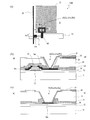
- FIGS. 1A to 1C show schematic structures of a TFT substrate 100A included in a liquid crystal display panel according to an embodiment of the present invention.
- the TFT substrate included in the liquid crystal display panel of the comparative example has the same structure as the TFT substrate 100A except that the surface roughness of the organic interlayer insulating layer is not within a predetermined range.
- FIGS. 1A to 1C are also referred to.
- FIG. 1A is a schematic plan view of a TFT substrate 100A included in the liquid crystal display panel according to the embodiment of the present invention, and shows a structure corresponding to one pixel (dot).
- 1B is a schematic cross-sectional view taken along the line 1B-1B ′ in FIG. 1A
- FIG. 1C is taken along the line 1C-1C ′ in FIG. It is a typical sectional view.
- the liquid crystal display panel includes a counter substrate disposed so as to face the TFT substrate 100A, and a liquid crystal provided between the TFT substrate 100A and the counter substrate. And further comprising a layer.
- the counter substrate includes, for example, a glass substrate, a color filter layer formed on the liquid crystal layer side of the glass substrate, and a black matrix (light shielding layer).
- An alignment film is typically formed on the surfaces of the TFT substrate 100A and the counter substrate that are in contact with the liquid crystal layer.
- a polarizing plate and a retardation plate are disposed outside the TFT substrate 100A and the counter substrate.
- the liquid crystal display panel of the embodiment according to the present invention is, for example, a VA mode or FFS mode liquid crystal display panel, and the constituent elements other than the TFT substrate 100A may be the same as those of a known liquid crystal display panel.
- a known VA mode and FFS mode liquid crystal display panel is described in, for example, Patent Document 3.
- Patent Document 3 For reference, the entire disclosure of Patent Document 3 is incorporated herein.
- a TFT substrate 100A used in a VA mode liquid crystal display panel will be described.
- the TFT substrate 100A includes a TFT supported on a substrate (for example, a glass substrate) 11, an organic interlayer insulating layer 24 covering the TFT, and a first transparent conductive layer 25 formed in a first region on the surface of the organic interlayer insulating layer 24. And an inorganic dielectric layer 26 containing SiN, which covers the first transparent conductive layer 25 and is formed in a second region different from the first region on the surface of the organic interlayer insulating layer 24, and has an organic interlayer insulating layer
- the arithmetic average roughness Ra of the first region and the second region of the surface of 24 is 3.45 nm or more and 5.20 nm or less.
- a region of the surface of the organic interlayer insulating layer 24 where the first transparent conductive layer 25 is in direct contact is called a first region
- a region where the inorganic dielectric layer 26 containing SiN is in direct contact is a second region.
- the arithmetic average roughness Ra of the first and second regions on the surface of the organic interlayer insulating layer 24 is controlled to be 3.45 nm or more and 5.20 nm or less.
- the entire surface of the organic interlayer insulating layer 24 is ashed in an oxygen-containing atmosphere to form an organic layer.
- the arithmetic average roughness Ra of the entire surface of the interlayer insulating layer 24 is controlled to be in the above range.
- the arithmetic average roughness Ra of the surface of the organic interlayer insulating layer 24 is in the above range, the generation of bubbles in the liquid crystal layer is suppressed. This is common to other liquid crystal display panels having the TFT substrate 100B shown in FIG. 4 according to the embodiment of the present invention.
- the TFT substrate 100A has a bottom gate type TFT supported by the substrate 11.
- An optional inorganic protective layer 12 is formed on the substrate 11, and a gate electrode 13 and a gate bus line 13 are formed thereon.
- the gate electrode 13 is formed as a part of the gate bus line 13, the same reference numerals are given for simplicity.
- a gate insulating layer 14 that covers substantially the entire surface of the substrate 11 is formed on the gate electrode 13, and a semiconductor layer 16 is formed so as to face the gate electrode 13 with the gate insulating layer 14 interposed therebetween.
- a source electrode 18s and a drain electrode 18d are formed on the semiconductor layer 16, and regions where the source electrode 18s and the drain electrode 18d are in contact with the semiconductor layer 16 become a source region and a drain region, respectively, and constitute a TFT.
- the TFT includes a gate electrode 13, a gate insulating layer 14, a semiconductor layer 16, a source electrode 18s, and a drain electrode 18d.
- the source bus line 18 is integrally formed from the same conductive film (source metal layer) as the source electrode 18s. Note that the structure of the TFT is not limited to this, and a wide variety of known TFTs can be used.
- An inorganic insulating layer 22 covering the TFT, the gate metal layer (the same conductive film as the gate bus line 13) and the source metal layer is formed.
- An organic interlayer insulating layer 24 is formed on the inorganic insulating layer 22.
- the organic interlayer insulating layer 24 also functions as a planarizing film.
- the surface of the organic interlayer insulating layer 24 has an arithmetic average roughness Ra of 3.45 nm to 5.20 nm.
- a first transparent conductive layer 25 is formed on the surface of the organic interlayer insulating layer 24.
- the TFT substrate 100A exemplified here is a TFT substrate 100A used in a VA mode liquid crystal display panel, and the first transparent conductive layer 25 is an auxiliary capacitance electrode. Since the auxiliary capacitance electrode 25 is typically provided in common to all the pixels, it is provided on almost the entire surface of the TFT substrate 100A.
- the auxiliary capacitance electrode 25 is provided with an opening as necessary.
- An inorganic dielectric layer 26 covering the auxiliary capacitance electrode 25 is formed on almost the entire surface of the substrate 11.
- the inorganic dielectric layer 26 is in direct contact with the organic interlayer insulating layer 24 in a region (second region) different from the region (first region) where the auxiliary capacitance electrode 25 is formed in the surface of the organic interlayer insulating layer 24. To do.
- a second transparent conductive layer 27 is formed in a predetermined region on the inorganic dielectric layer 26.
- the pixel electrode 27, the auxiliary capacitance electrode 25, and the inorganic dielectric layer 26 located between the pixel electrode 27 and the auxiliary capacitance electrode 25 form an auxiliary capacitance.
- the auxiliary capacitor electrode 25 is supplied with a common voltage supplied to a counter electrode provided on a counter substrate (a substrate disposed so as to face the TFT substrate 100A via a liquid crystal layer). Since the auxiliary capacitance electrode 25 is transparent, even if it exists in the pixel region, the influence on the pixel aperture ratio of the liquid crystal display panel is limited.
- the area of the auxiliary capacitance electrode 25 that forms the auxiliary capacitance (that is, faces the pixel electrode 27 with the inorganic dielectric layer 26 therebetween) is adjusted. Is done.
- the pixel electrode 27 is in contact with the drain electrode 18d in the contact hole 28.
- the contact hole 28 includes a contact hole 22 a formed in the inorganic insulating layer 22, a contact hole 24 a formed in the organic interlayer insulating layer 24, and a contact hole 26 a formed in the inorganic dielectric layer 26.
- the inner peripheral surface of the contact hole 24 a of the organic interlayer insulating layer 24 is covered with an inorganic dielectric layer 26.
- the pixel electrode 27 formed on the inorganic dielectric layer 26 is also formed on the inorganic dielectric layer 26 covering the inner peripheral surface of the contact hole 24a, and in the contact hole 26a included in the inorganic dielectric layer 26. In contact with the drain electrode 18d.
- the first transparent conductive layer 25 functions as a common electrode (counter electrode) 25, and the common electrode 25 and a plurality of parallel electrodes extend in parallel to each other.
- a horizontal electric field is generated between the pixel electrode 27 having a straight line portion.
- the first transparent conductive layer 25 may be used as the pixel electrode 25 and the second transparent conductive layer 27 may be used as the common electrode (counter electrode) 27.
- the illustrated TFT substrate 100A can be manufactured by a known method using a known material.
- the inorganic protective layer 12 formed as necessary can be formed in the same manner as the gate insulating layer 14 or the inorganic insulating layer 22 described later.
- the inorganic protective layer 12 has a function of preventing diffusion of ions from the substrate 11, for example.
- the thickness of the inorganic protective layer 12 is, for example, not less than 50 nm and not more than 200 nm.
- the gate metal layer As a material of the gate metal layer, a metal such as aluminum (Al), tungsten (W), molybdenum (Mo), tantalum (Ta), chromium (Cr), titanium (Ti), copper (Cu), or an alloy thereof, or an alloy thereof, or an alloy thereof, or The nitride can be used.
- the gate metal layer is formed by, for example, a sputtering method.
- the gate electrode 13 and the gate bus line 13 can be formed by patterning the gate metal layer by a photolithography process.
- the thickness of the gate metal layer is, for example, not less than 100 nm and not more than 400 nm.
- Examples of the material of the gate insulating layer 14 include silicon dioxide (SiO 2 ), silicon nitride (SiN x ), silicon oxynitride (SiO x N y , x> y), and silicon nitride oxide (SiN x O y , x>). y) and the like can be used.
- the gate insulating layer 14 may be a single layer film or a laminated film.
- the gate insulating layer 14 is formed by, for example, a CVD method and / or a sputtering method.
- the thickness of the gate insulating layer 14 is, for example, not less than 100 nm and not more than 500 nm.
- the semiconductor layer 16 is, for example, an oxide semiconductor layer.
- the oxide semiconductor layer includes, for example, an In—Ga—Zn—O-based semiconductor (hereinafter abbreviated as “In—Ga—Zn—O-based semiconductor”).
- a TFT having an In—Ga—Zn—O-based semiconductor layer has high mobility (more than 20 times that of an a-Si TFT) and low leakage current (less than one hundredth of that of an a-Si TFT). It is suitably used as a drive TFT and a pixel TFT. If a TFT having an In—Ga—Zn—O-based semiconductor layer is used, the power consumption of the liquid crystal display panel can be significantly reduced.
- the In—Ga—Zn—O based semiconductor may be amorphous or may contain a crystalline part.
- a crystalline In—Ga—Zn—O-based semiconductor in which the c-axis is oriented substantially perpendicular to the layer surface is preferable.
- Such a crystal structure of an In—Ga—Zn—O-based semiconductor is disclosed in, for example, Japanese Patent Laid-Open No. 2012-134475. For reference, the entire disclosure of Japanese Patent Application Laid-Open No. 2012-134475 is incorporated herein by reference.
- the oxide semiconductor layer may include another oxide semiconductor instead of the In—Ga—Zn—O-based semiconductor.
- Zn—O based semiconductor ZnO
- In—Zn—O based semiconductor IZO (registered trademark)
- Zn—Ti—O based semiconductor ZTO
- Cd—Ge—O based semiconductor Cd—Pb—O based
- CdO cadmium oxide
- Mg—Zn—O based semiconductors In—Sn—Zn—O based semiconductors (eg, In 2 O 3 —SnO 2 —ZnO), In—Ga—Sn—O based semiconductors, etc. You may go out.
- the semiconductor layer 16 is not limited to an oxide semiconductor layer, and a silicon-based material such as amorphous silicon, polysilicon, microcrystalline silicon, or continuous grain boundary crystalline silicon may be used.
- the thickness of the semiconductor layer 16 is, for example, not less than 10 nm and not more than 100 nm.
- the source metal layer As a material of the source metal layer, a metal such as aluminum (Al), molybdenum (Mo), copper (Cu), titanium (Ti) or an alloy thereof, or a nitride thereof can be used.
- the source metal layer may be not only a single layer film formed from the above material but also a laminated film formed from the above material.
- the source metal layer may be transparent.
- ITO indium tin oxide
- IZO indium zinc oxide
- InZnO-based transparent conductive material indium tin oxide containing silicon oxide
- the source metal layer may be formed using a light-transmitting conductive material such as ITSO), indium oxide (In 2 O 3 ), tin oxide (SnO 2 ), zinc oxide (ZnO), or titanium oxide. Moreover, you may use combining these suitably.
- the source metal layer is formed by, for example, a sputtering method. By patterning the source metal layer, a source metal layer including the source electrode 18s and the drain electrode 18d is formed.
- the thickness of the source metal layer is, for example, not less than 100 nm and not more than 400 nm.
- Examples of the material of the inorganic insulating layer 22 include silicon dioxide (SiO 2 ), silicon nitride (SiN x ), silicon oxynitride (SiO x N y , x> y), and silicon nitride oxide (SiN x O y , x>). y) and the like can be used.
- the inorganic insulating layer 22 may be a single layer film or a laminated film of two or more layers.
- the inorganic insulating layer 22 is formed by, for example, a CVD method.
- the thickness of the inorganic insulating layer 22 is, for example, not less than 150 nm and not more than 700 nm.
- a photosensitive resin material can be used as the material of the organic interlayer insulating layer 24, for example, a photosensitive resin material can be used.
- the photosensitive resin material is, for example, a positive photosensitive resin material (for example, an acrylic resin material).
- a negative photosensitive resin material can also be used.
- An organic interlayer insulating layer having a contact hole 24a is formed by applying a photosensitive resin material on the inorganic insulating layer 22 by a coating method or a printing method and then patterning the film of the photosensitive resin material using a photolithography process. 24 is formed.
- the inorganic insulating layer 22 is exposed in the contact hole 24a.
- the thickness of the organic interlayer insulating layer 24 is, for example, 2 ⁇ m or more and 4 ⁇ m or less.
- the inorganic insulating layer 22 is dry-etched using the organic interlayer insulating layer 24 as a mask, thereby forming a contact hole 22a in the inorganic insulating layer 22.
- the drain electrode 18d is exposed in the contact holes 22a and 24a.
- the surface of the organic interlayer insulating layer 24 is ashed.
- the arithmetic average roughness Ra of the surface of the organic interlayer insulating layer 24 is set to 3.45 nm or more and 5.20 nm or less by ashing.
- Ashing is preferably performed in a gas atmosphere containing oxygen.
- the surface having the above-mentioned predetermined roughness is obtained by ashing under the conditions of an RF power of 2000 W, a pressure of 30 mTorr, an oxygen flow rate of 50 sccm, and an application time of 60 s, as will be described in detail later with an experimental example. Can be formed.
- the surface of the ashed organic interlayer insulating layer 24 is oxidized and becomes hydrophilic, and the adhesiveness with the auxiliary capacitance electrode 25 and the inorganic dielectric layer 26 is excellent.
- the auxiliary capacitance electrode 25 is formed using a transparent conductive material.
- a transparent conductive material InZnO-based transparent conductive material, indium tin oxide (ITO), or the like can be used.
- the auxiliary capacitance electrode 25 is formed by, for example, patterning a layer of a transparent conductive material formed by a sputtering method using a photolithography process.
- the thickness of the auxiliary capacitance electrode 25 is, for example, not less than 50 nm and not more than 150 nm.
- an InZnO-based transparent conductive material is used on the surface of the organic interlayer insulating layer 24 having an arithmetic average roughness Ra of 3.45 nm to 5.20 nm.
- a transparent conductive layer serving as the auxiliary capacitance electrode 25 is deposited under the conditions of power 1 W / cm 2 , oxygen partial pressure 5%, 0.6 Pa, and deposition time 200 s, the arithmetic average roughness Ra is 3.75 nm or more and 6.30 nm or less.
- This transparent conductive layer is an amorphous layer having a columnar structure, and has excellent adhesion to the organic interlayer insulating layer 24.
- the inorganic dielectric layer 26 includes SiN, for example, using silicon nitride (SiN x ), silicon oxynitride (SiO x N y , x> y), silicon nitride oxide (SiN x O y , x> y). Can be formed. Further, a layer containing these SiN and a layer of silicon dioxide (SiO 2 ) may be stacked.
- the thickness of the inorganic dielectric layer 26 is, for example, not less than 50 nm and not more than 400 nm.
- the process of forming the inorganic dielectric layer 26 containing SiN includes a CVD process using SiH 4 and NH 3 as reaction gases. According to the study by the present inventor, it was found that at this time, the gas of SiH 4 and / or H 2 was taken into the organic interlayer insulating layer 24 and this was the cause of bubbles generated in the liquid crystal layer. .
- the arithmetic average roughness Ra of the surface of the region where the organic interlayer insulating layer 24 is in contact with the auxiliary capacitance electrode 25 or the inorganic dielectric layer 26 is 3.45 nm or more and 5.20 nm. Since it is controlled as follows, SiH 4 or H 2 gas taken into the organic interlayer insulating layer 24 is suppressed from being released from the organic interlayer insulating layer 24 during use of the liquid crystal display panel.
- the TFT substrate 100 ⁇ / b> A exemplified here has a pixel electrode 27 on the inorganic dielectric layer 26.
- the pixel electrode 27 is formed using a transparent conductive material, like the auxiliary capacitance electrode 25.
- the pixel electrode 27 is formed so as to be in contact with the drain electrode 18d exposed in the contact hole 28 (22a, 24a, 26a) and patterned so as to have a predetermined shape.
- an alignment film (not shown) is formed on almost the entire surface so as to cover the surface of the TFT substrate 100A on the liquid crystal layer side, and used for the assembly process of the liquid crystal display panel.
- the inventor omits the step of ashing the surface of the organic interlayer insulating layer 24 in the manufacturing method of the TFT substrate 100A described above or changes the ashing time (30 seconds, 60 seconds, 90 seconds), A TFT substrate was produced.
- a liquid crystal display panel was produced using the produced TFT substrate.
- the manufactured TFT substrate is called a TFT substrate (0), a TFT substrate (30), a TFT substrate (60), and a TFT substrate (90) according to the ashing time (seconds).
- a liquid crystal display panel using these is called It will be referred to as LCD (0), LCD (30), LCD (60), and LCD (90).
- the TFT substrate has the following configuration.
- the inorganic protective layer 12 was omitted.
- Substrate 11 Glass substrate thickness 0.7mm
- Gate metal layer W layer / TaN layer, thickness 400 nm (350 nm / 50 nm), sputtering method
- Gate insulating layer 14 SiO 2 layer, thickness 400 nm, sputtering method
- Semiconductor layer 16 In—Ga—Zn—O-based semiconductor layer , Thickness 50 nm, sputtering method
- Source metal layer Ti / Al / Ti layer, thickness 400 nm (100 nm / 200 nm / 100 nm), sputtering method
- Inorganic insulating layer 22 SiO 2 layer, thickness 250 nm
- Organic interlayer insulating layer 24 Positive acrylic resin layer, thickness 2 ⁇ m, post-baking 220 ° C., 60 minutes Ashing conditions: RF power 2000 W, pressure 30 mTorr (4 Pa), oxygen flow rate
- FIGS. 2A to 2D show the surface of the organic interlayer insulating layer 24 in the process of manufacturing the TFT substrate (0), TFT substrate (30), TFT substrate (60), and TFT substrate (90).
- the image observed with the microscope (AFM, Bruker AXS company make, "NanoscopeV" is shown. One side of each image is 1 ⁇ m. Further, the arithmetic average roughness Ra and the root mean square roughness Rq of the surface of the organic interlayer insulating layer 24 were determined by AFM. The results are shown in Table 1.
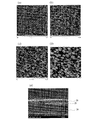
- FIGS. 3A to 3D show the auxiliary capacitor electrode (first transparent conductive layer) in the manufacturing process of the TFT substrate (0), TFT substrate (30), TFT substrate (60), and TFT substrate (90).
- the image which observed the surface of 25 with the atomic force microscope is shown. One side of each image is 1 ⁇ m. Further, the arithmetic average roughness Ra and the root mean square roughness Rq of the surface of the auxiliary capacitance electrode 25 were obtained by AFM. The results are shown in Table 2.
- 3A to 3D and Table 2 show that the surface roughness of the auxiliary capacitance electrode 25 formed on the organic interlayer insulating layer 24 with a longer ashing time increases. That is, it can be seen that the surface roughness of the auxiliary capacitance electrode 25 reflects the surface roughness of the underlying organic interlayer insulating layer 24.
- the InZnO-based transparent conductive layer constituting the auxiliary capacitance electrode 25 has a columnar structure.
- This InZnO-based transparent conductive layer is amorphous and has a columnar structure, so that it is densified, and SiH 4 and / or H 2 gas taken into the organic interlayer insulating layer 24 leaks into the liquid crystal layer. It is thought that it contributes to suppression.
- the ashing time exceeds 90 seconds, the film thickness of the organic interlayer insulating layer 24 is large and the surface roughness is large. As a result, the yield of the first transparent conductive layer 25 may be reduced, and thus the ashing time is preferably 90 seconds or less.
- the ashing conditions and / or time are appropriately set so that the arithmetic average roughness Ra of the surface of the organic interlayer insulating layer 24 is 3.45 nm or more and 5.20 nm or less. Adjust it.
- the transparent conductive layer 25 formed on the surface of the organic interlayer insulating layer 24 is preferably formed so that the arithmetic average roughness Ra of the surface is 3.75 nm or more and 6.30 nm or less.
- the arithmetic average roughness Ra (nm) is used as a parameter characterizing the surface roughness of the organic interlayer insulating layer 24 and the transparent conductive layer 25 formed on the surface of the organic interlayer insulating layer 24.
- the root mean square roughness Rq (nm) can also be used. That is, the root mean square roughness Rq of the surface of the organic interlayer insulating layer 24 is 4.35 nm to 6.67 nm, and the root mean square roughness Rq of the surface of the transparent conductive layer 25 is 4.69 nm to 7.85 nm. It is.
- FIG. 4A to 4C show schematic structures of other TFT substrates 100B included in the liquid crystal display panel according to the embodiment of the present invention.
- FIG. 4A is a schematic plan view of another TFT substrate 100B included in the liquid crystal display panel according to the embodiment of the present invention, and shows a structure corresponding to one pixel (dot).
- 4B is a schematic cross-sectional view taken along line 4B-4B ′ in FIG. 4A
- FIG. 4C is taken along line 4C-4C ′ in FIG. 4A. It is a typical sectional view.
- the pixel electrode 27 includes a contact hole 22a included in the inorganic insulating layer 22, a first contact hole 24a included in the organic interlayer insulating layer 24, and a second contact hole 26a included in the inorganic dielectric layer 26.
- the contact hole 28 is connected to the drain electrode 18 d of the thin film transistor, and the first contact hole 24 a and the second contact hole 26 a intersect each other when viewed from the normal direction of the substrate 11. Since the TFT substrate 100B may have substantially the same structure as the TFT substrate 100A except that the structure of the contact hole 28 is different, the description thereof is omitted.
- the drain electrode 18d is arranged so as to overlap the pixel electrode 27. Since the area of the portion can be reduced, the pixel aperture ratio can be improved.
- the contact hole 22a and the first contact hole 24a are arranged in parallel.
- the TFT substrate having the pixel electrode 27 on the liquid crystal layer side and the pixel electrode 27 having a plurality of slits is exemplified as the TFT substrate used in the VA mode liquid crystal display panel, but according to the embodiment of the present invention.
- the liquid crystal display panel and the TFT substrate used for the liquid crystal display panel are not limited to this, and can be used for an FFS mode liquid crystal display panel.
- the liquid crystal display panel according to the embodiment of the present invention can be applied to a liquid crystal display panel of a vertical electric field mode other than the VA mode and a horizontal electric field mode other than the FFS mode.
- the present invention can be widely applied to liquid crystal display panels.
Landscapes
- Physics & Mathematics (AREA)
- Nonlinear Science (AREA)
- Mathematical Physics (AREA)
- Chemical & Material Sciences (AREA)
- Crystallography & Structural Chemistry (AREA)
- General Physics & Mathematics (AREA)
- Optics & Photonics (AREA)
- Engineering & Computer Science (AREA)
- Microelectronics & Electronic Packaging (AREA)
- Geometry (AREA)
- Liquid Crystal (AREA)
- Thin Film Transistor (AREA)
Abstract
Description
基板11:ガラス基板 厚さ0.7mm
ゲートメタル層:W層/TaN層、厚さ400nm(350nm/50nm)、スパッタリング法
ゲート絶縁層14:SiO2層、厚さ400nm、スパッタリング法
半導体層16:In-Ga-Zn-O系半導体層、厚さ50nm、スパッタリング法
ソースメタル層:Ti/Al/Ti層、厚さ400nm(100nm/200nm/100nm)、スパッタリング法
無機絶縁層22:SiO2層、厚さ250nm、スパッタリング法
有機層間絶縁層24:ポジ型アクリル樹脂層、厚さ2μm、ポストベーク220℃、60分
アッシング条件:RFパワー2000W、圧力30mTorr(4Pa)、酸素流量50sccm、印加時間60s
補助容量電極25:InZnO系透明導電層、厚さ100nm、スパッタリング法
無機誘電体層26:窒化珪素(SiNx)層、厚さ200nm、CVD法


12 無機保護層
13 ゲート電極、ゲートバスライン
14 ゲート絶縁層
16 半導体層
18 ソースバスライン
18s ソース電極
18d ドレイン電極
22 無機絶縁層
24 有機層間絶縁層
25 補助容量電極(第1透明導電層)
26 無機誘電体層
27 画素電極(第2透明導電層)
28 コンタクトホール
100A、100B TFT基板
Claims (7)
- 液晶層と、
前記液晶層を介して互いに対向するように配置された第1および第2基板と、
前記第1基板に支持された薄膜トランジスタと、
前記薄膜トランジスタを覆う有機層間絶縁層と、
前記有機層間絶縁層の表面の第1領域に形成された第1透明導電層と、
前記第1透明導電層を覆い、かつ、前記有機層間絶縁層の前記表面の前記第1領域と異なる第2領域に形成されたSiNを含む無機誘電体層と
を有し、
前記有機層間絶縁層の前記表面の前記第1領域および前記第2領域の算術平均粗さRaは3.45nm以上5.20nm以下である、液晶表示パネル。 - 前記第1透明導電層の表面の算術平均粗さRaは3.75nm以上6.30nm以下である、請求項1に記載の液晶表示パネル。
- 前記無機誘電体層の上に、第2透明導電層を有する、請求項1または2に記載の液晶表示パネル。
- 前記第2透明導電層は、前記有機層間絶縁層が有する第1コンタクトホールと、前記無機誘電体層が有する第2コンタクトホールとを含むコンタクトホール内で、前記薄膜トランジスタのドレイン電極に接続されており、前記第1コンタクトホールの内周面は、前記無機誘電体層で覆われている、請求項3に記載の液晶表示パネル。
- 前記第2透明導電層は、前記有機層間絶縁層が有する第1コンタクトホールと、前記無機誘電体層が有する第2コンタクトホールとを含むコンタクトホール内で、前記薄膜トランジスタのドレイン電極に接続されており、前記第1コンタクトホールと、前記第2コンタクトホールとは、前記第1基板の法線方向から見たとき、互いに交差している、請求項3に記載の液晶表示パネル。
- 液晶層と、前記液晶層を介して互いに対向するように配置された第1および第2基板とを有する液晶表示パネルの製造方法であって、
第1基板を用意する工程と、
前記第1基板上に薄膜トランジスタを形成する工程と、
前記薄膜トランジスタを覆う有機層間絶縁層を形成する工程と、
前記有機層間絶縁層の表面をアッシングすることによって、算術平均粗さRaが3.45nm以上5.20nm以下である第1領域および第2領域を形成する工程と、
前記有機層間絶縁層の前記第1領域に第1透明導電層を形成する工程と、
前記第1透明導電層を覆い、かつ、前記有機層間絶縁層の前記表面の前記第1領域と異なる前記第2領域にSiNを含む無機誘電体層をCVD法で形成する工程と
を包含する、液晶表示パネルの製造方法。 - 前記アッシングは、酸素を含むガス雰囲気下で行われる、請求項6に記載の液晶表示パネルの製造方法。
Priority Applications (3)
| Application Number | Priority Date | Filing Date | Title |
|---|---|---|---|
| US15/304,114 US9690155B2 (en) | 2014-04-16 | 2015-04-09 | Liquid crystal display panel and method for producing same |
| JP2016513747A JP6186077B2 (ja) | 2014-04-16 | 2015-04-09 | 液晶表示パネルおよびその製造方法 |
| CN201580019855.1A CN106233196B (zh) | 2014-04-16 | 2015-04-09 | 液晶显示面板及其制造方法 |
Applications Claiming Priority (2)
| Application Number | Priority Date | Filing Date | Title |
|---|---|---|---|
| JP2014084862 | 2014-04-16 | ||
| JP2014-084862 | 2014-04-16 |
Publications (1)
| Publication Number | Publication Date |
|---|---|
| WO2015159800A1 true WO2015159800A1 (ja) | 2015-10-22 |
Family
ID=54324009
Family Applications (1)
| Application Number | Title | Priority Date | Filing Date |
|---|---|---|---|
| PCT/JP2015/061125 Ceased WO2015159800A1 (ja) | 2014-04-16 | 2015-04-09 | 液晶表示パネルおよびその製造方法 |
Country Status (5)
| Country | Link |
|---|---|
| US (1) | US9690155B2 (ja) |
| JP (1) | JP6186077B2 (ja) |
| CN (1) | CN106233196B (ja) |
| TW (1) | TWI585497B (ja) |
| WO (1) | WO2015159800A1 (ja) |
Cited By (2)
| Publication number | Priority date | Publication date | Assignee | Title |
|---|---|---|---|---|
| WO2018139450A1 (ja) * | 2017-01-27 | 2018-08-02 | シャープ株式会社 | アクティブマトリクス基板およびそれを用いた表示装置 |
| JP2019074684A (ja) * | 2017-10-18 | 2019-05-16 | シャープ株式会社 | 表示パネル用基板の製造方法 |
Families Citing this family (2)
| Publication number | Priority date | Publication date | Assignee | Title |
|---|---|---|---|---|
| JP2017168806A (ja) * | 2015-12-21 | 2017-09-21 | ソニー株式会社 | 撮像素子、固体撮像装置及び電子デバイス |
| JP2017126014A (ja) * | 2016-01-15 | 2017-07-20 | 株式会社ジャパンディスプレイ | 表示装置 |
Citations (4)
| Publication number | Priority date | Publication date | Assignee | Title |
|---|---|---|---|---|
| WO2010038514A1 (ja) * | 2008-10-02 | 2010-04-08 | シャープ株式会社 | 表示装置用基板、表示装置用基板の製造方法、表示装置、液晶表示装置、液晶表示装置の製造方法及び有機エレクトロルミネセンス表示装置 |
| JP2010160530A (ja) * | 2010-04-26 | 2010-07-22 | Sony Corp | 液晶表示素子および表示装置 |
| JP2011100041A (ja) * | 2009-11-09 | 2011-05-19 | Hitachi Displays Ltd | 液晶表示装置の製造方法 |
| JP2013025256A (ja) * | 2011-07-25 | 2013-02-04 | Japan Display Central Co Ltd | 液晶表示装置及びその製造方法 |
Family Cites Families (8)
| Publication number | Priority date | Publication date | Assignee | Title |
|---|---|---|---|---|
| JP2933879B2 (ja) | 1995-08-11 | 1999-08-16 | シャープ株式会社 | 透過型液晶表示装置およびその製造方法 |
| JP3634702B2 (ja) * | 1999-02-25 | 2005-03-30 | キヤノン株式会社 | 電子源基板及び画像形成装置 |
| JP3724787B2 (ja) | 2000-03-31 | 2005-12-07 | シャープ株式会社 | 電極基板およびその作製方法、ならびに、電極基板を備える液晶表示装置 |
| JP4115761B2 (ja) * | 2002-07-05 | 2008-07-09 | アルプス電気株式会社 | アクティブマトリクス基板及びその製造方法並びにそれを用いた表示装置 |
| CN102576735B (zh) * | 2009-09-30 | 2016-01-20 | 大日本印刷株式会社 | 挠性装置用基板、挠性装置用薄膜晶体管基板、挠性装置、薄膜元件用基板、薄膜元件、薄膜晶体管、薄膜元件用基板的制造方法、薄膜元件的制造方法及薄膜晶体管的制造方法 |
| CN103339715B (zh) | 2010-12-03 | 2016-01-13 | 株式会社半导体能源研究所 | 氧化物半导体膜以及半导体装置 |
| US9507225B2 (en) | 2011-11-15 | 2016-11-29 | Sharp Kabushiki Kaisha | Active matrix substrate and liquid crystal display panel equipped with same |
| JPWO2014046025A1 (ja) * | 2012-09-21 | 2016-08-18 | シャープ株式会社 | 液晶ディスプレイ |
-
2015
- 2015-04-09 CN CN201580019855.1A patent/CN106233196B/zh not_active Expired - Fee Related
- 2015-04-09 JP JP2016513747A patent/JP6186077B2/ja active Active
- 2015-04-09 WO PCT/JP2015/061125 patent/WO2015159800A1/ja not_active Ceased
- 2015-04-09 US US15/304,114 patent/US9690155B2/en not_active Expired - Fee Related
- 2015-04-16 TW TW104112247A patent/TWI585497B/zh not_active IP Right Cessation
Patent Citations (4)
| Publication number | Priority date | Publication date | Assignee | Title |
|---|---|---|---|---|
| WO2010038514A1 (ja) * | 2008-10-02 | 2010-04-08 | シャープ株式会社 | 表示装置用基板、表示装置用基板の製造方法、表示装置、液晶表示装置、液晶表示装置の製造方法及び有機エレクトロルミネセンス表示装置 |
| JP2011100041A (ja) * | 2009-11-09 | 2011-05-19 | Hitachi Displays Ltd | 液晶表示装置の製造方法 |
| JP2010160530A (ja) * | 2010-04-26 | 2010-07-22 | Sony Corp | 液晶表示素子および表示装置 |
| JP2013025256A (ja) * | 2011-07-25 | 2013-02-04 | Japan Display Central Co Ltd | 液晶表示装置及びその製造方法 |
Cited By (6)
| Publication number | Priority date | Publication date | Assignee | Title |
|---|---|---|---|---|
| WO2018139450A1 (ja) * | 2017-01-27 | 2018-08-02 | シャープ株式会社 | アクティブマトリクス基板およびそれを用いた表示装置 |
| CN110226193A (zh) * | 2017-01-27 | 2019-09-10 | 夏普株式会社 | 有源矩阵基板以及使用它的显示装置 |
| JPWO2018139450A1 (ja) * | 2017-01-27 | 2019-11-14 | シャープ株式会社 | アクティブマトリクス基板およびそれを用いた表示装置 |
| US10725352B2 (en) | 2017-01-27 | 2020-07-28 | Sharp Kabushiki Kaisha | Active matrix substrate and display device using same |
| JP2019074684A (ja) * | 2017-10-18 | 2019-05-16 | シャープ株式会社 | 表示パネル用基板の製造方法 |
| US10620468B2 (en) | 2017-10-18 | 2020-04-14 | Sharp Kabushiki Kaisha | Method of manufacturing display panel substrate |
Also Published As
| Publication number | Publication date |
|---|---|
| CN106233196B (zh) | 2019-05-07 |
| JP6186077B2 (ja) | 2017-08-23 |
| US20170038651A1 (en) | 2017-02-09 |
| CN106233196A (zh) | 2016-12-14 |
| TWI585497B (zh) | 2017-06-01 |
| US9690155B2 (en) | 2017-06-27 |
| JPWO2015159800A1 (ja) | 2017-04-13 |
| TW201546530A (zh) | 2015-12-16 |
Similar Documents
| Publication | Publication Date | Title |
|---|---|---|
| US10276593B2 (en) | Active matrix substrate and method for manufacturing same, display device using active matrix substrate | |
| CN105514116B (zh) | Tft背板结构及其制作方法 | |
| US9236405B2 (en) | Array substrate, manufacturing method and the display device thereof | |
| TWI519876B (zh) | 主動矩陣型基板 | |
| CN101326644A (zh) | 薄膜晶体管及其制造方法 | |
| WO2015098183A1 (ja) | アクティブマトリクス基板の製造方法および表示装置の製造方法ならびに表示装置 | |
| TW201611252A (zh) | 半導體裝置、液晶顯示裝置及半導體裝置的製造方法 | |
| US20190243194A1 (en) | Active matrix substrate and method for manufacturing same | |
| JP6186077B2 (ja) | 液晶表示パネルおよびその製造方法 | |
| WO2015192595A1 (zh) | 阵列基板及其制备方法、显示装置 | |
| JP2016122683A (ja) | 薄膜トランジスタ基板およびその製造方法 | |
| TW201322456A (zh) | 薄膜電晶體及其製造方法 | |
| US20160336359A1 (en) | Thin film transistor device, manufacturing method thereof, and display apparatus | |
| JP5636304B2 (ja) | 薄膜トランジスタ回路基板及びその製造方法 | |
| WO2016123979A1 (zh) | 薄膜晶体管及其制备方法、阵列基板和显示装置 | |
| JP6286453B2 (ja) | 半導体装置およびその製造方法 | |
| WO2020066287A1 (ja) | 薄膜トランジスタ、表示装置及び薄膜トランジスタの製造方法 | |
| KR20140014546A (ko) | 표시 장치 및 그 제조 방법 | |
| CN103003744B (zh) | 液晶显示装置及其制造方法 | |
| CN102751333A (zh) | 主动元件及其制造方法 | |
| US20150048360A1 (en) | Semiconductor device and semiconductor device manufacturing method | |
| US11488990B2 (en) | Active matrix substrate and production method thereof | |
| US10199396B2 (en) | Display device having improved manufacturability and method for fabricating same | |
| WO2011148728A1 (ja) | 表示装置およびその製造方法 | |
| WO2013008359A1 (ja) | 液晶表示装置およびその製造方法 |
Legal Events
| Date | Code | Title | Description |
|---|---|---|---|
| 121 | Ep: the epo has been informed by wipo that ep was designated in this application |
Ref document number: 15780311 Country of ref document: EP Kind code of ref document: A1 |
|
| ENP | Entry into the national phase |
Ref document number: 2016513747 Country of ref document: JP Kind code of ref document: A |
|
| WWE | Wipo information: entry into national phase |
Ref document number: 15304114 Country of ref document: US |
|
| NENP | Non-entry into the national phase |
Ref country code: DE |
|
| 122 | Ep: pct application non-entry in european phase |
Ref document number: 15780311 Country of ref document: EP Kind code of ref document: A1 |