WO2015152123A1 - マスクブランク、転写用マスクの製造方法及び半導体装置の製造方法 - Google Patents
マスクブランク、転写用マスクの製造方法及び半導体装置の製造方法 Download PDFInfo
- Publication number
- WO2015152123A1 WO2015152123A1 PCT/JP2015/059852 JP2015059852W WO2015152123A1 WO 2015152123 A1 WO2015152123 A1 WO 2015152123A1 JP 2015059852 W JP2015059852 W JP 2015059852W WO 2015152123 A1 WO2015152123 A1 WO 2015152123A1
- Authority
- WO
- WIPO (PCT)
- Prior art keywords
- film
- light
- pattern
- mask
- shielding film
- Prior art date
- Legal status (The legal status is an assumption and is not a legal conclusion. Google has not performed a legal analysis and makes no representation as to the accuracy of the status listed.)
- Ceased
Links
Images





Classifications
-
- G—PHYSICS
- G03—PHOTOGRAPHY; CINEMATOGRAPHY; ANALOGOUS TECHNIQUES USING WAVES OTHER THAN OPTICAL WAVES; ELECTROGRAPHY; HOLOGRAPHY
- G03F—PHOTOMECHANICAL PRODUCTION OF TEXTURED OR PATTERNED SURFACES, e.g. FOR PRINTING, FOR PROCESSING OF SEMICONDUCTOR DEVICES; MATERIALS THEREFOR; ORIGINALS THEREFOR; APPARATUS SPECIALLY ADAPTED THEREFOR
- G03F1/00—Originals for photomechanical production of textured or patterned surfaces, e.g., masks, photo-masks, reticles; Mask blanks or pellicles therefor; Containers specially adapted therefor; Preparation thereof
- G03F1/26—Phase shift masks [PSM]; PSM blanks; Preparation thereof
- G03F1/32—Attenuating PSM [att-PSM], e.g. halftone PSM or PSM having semi-transparent phase shift portion; Preparation thereof
-
- G—PHYSICS
- G03—PHOTOGRAPHY; CINEMATOGRAPHY; ANALOGOUS TECHNIQUES USING WAVES OTHER THAN OPTICAL WAVES; ELECTROGRAPHY; HOLOGRAPHY
- G03F—PHOTOMECHANICAL PRODUCTION OF TEXTURED OR PATTERNED SURFACES, e.g. FOR PRINTING, FOR PROCESSING OF SEMICONDUCTOR DEVICES; MATERIALS THEREFOR; ORIGINALS THEREFOR; APPARATUS SPECIALLY ADAPTED THEREFOR
- G03F1/00—Originals for photomechanical production of textured or patterned surfaces, e.g., masks, photo-masks, reticles; Mask blanks or pellicles therefor; Containers specially adapted therefor; Preparation thereof
- G03F1/20—Masks or mask blanks for imaging by charged particle beam [CPB] radiation, e.g. by electron beam; Preparation thereof
-
- G—PHYSICS
- G03—PHOTOGRAPHY; CINEMATOGRAPHY; ANALOGOUS TECHNIQUES USING WAVES OTHER THAN OPTICAL WAVES; ELECTROGRAPHY; HOLOGRAPHY
- G03F—PHOTOMECHANICAL PRODUCTION OF TEXTURED OR PATTERNED SURFACES, e.g. FOR PRINTING, FOR PROCESSING OF SEMICONDUCTOR DEVICES; MATERIALS THEREFOR; ORIGINALS THEREFOR; APPARATUS SPECIALLY ADAPTED THEREFOR
- G03F1/00—Originals for photomechanical production of textured or patterned surfaces, e.g., masks, photo-masks, reticles; Mask blanks or pellicles therefor; Containers specially adapted therefor; Preparation thereof
- G03F1/38—Masks having auxiliary features, e.g. special coatings or marks for alignment or testing; Preparation thereof
- G03F1/48—Protective coatings
-
- G—PHYSICS
- G03—PHOTOGRAPHY; CINEMATOGRAPHY; ANALOGOUS TECHNIQUES USING WAVES OTHER THAN OPTICAL WAVES; ELECTROGRAPHY; HOLOGRAPHY
- G03F—PHOTOMECHANICAL PRODUCTION OF TEXTURED OR PATTERNED SURFACES, e.g. FOR PRINTING, FOR PROCESSING OF SEMICONDUCTOR DEVICES; MATERIALS THEREFOR; ORIGINALS THEREFOR; APPARATUS SPECIALLY ADAPTED THEREFOR
- G03F1/00—Originals for photomechanical production of textured or patterned surfaces, e.g., masks, photo-masks, reticles; Mask blanks or pellicles therefor; Containers specially adapted therefor; Preparation thereof
- G03F1/68—Preparation processes not covered by groups G03F1/20 - G03F1/50
- G03F1/80—Etching
-
- H—ELECTRICITY
- H10—SEMICONDUCTOR DEVICES; ELECTRIC SOLID-STATE DEVICES NOT OTHERWISE PROVIDED FOR
- H10P—GENERIC PROCESSES OR APPARATUS FOR THE MANUFACTURE OR TREATMENT OF DEVICES COVERED BY CLASS H10
- H10P50/00—Etching of wafers, substrates or parts of devices
- H10P50/60—Wet etching
- H10P50/64—Wet etching of semiconductor materials
- H10P50/642—Chemical etching
-
- H—ELECTRICITY
- H10—SEMICONDUCTOR DEVICES; ELECTRIC SOLID-STATE DEVICES NOT OTHERWISE PROVIDED FOR
- H10P—GENERIC PROCESSES OR APPARATUS FOR THE MANUFACTURE OR TREATMENT OF DEVICES COVERED BY CLASS H10
- H10P50/00—Etching of wafers, substrates or parts of devices
- H10P50/69—Etching of wafers, substrates or parts of devices using masks for semiconductor materials
- H10P50/691—Etching of wafers, substrates or parts of devices using masks for semiconductor materials for Group V materials or Group III-V materials
- H10P50/692—Etching of wafers, substrates or parts of devices using masks for semiconductor materials for Group V materials or Group III-V materials characterised by their composition, e.g. multilayer masks or materials
-
- H—ELECTRICITY
- H10—SEMICONDUCTOR DEVICES; ELECTRIC SOLID-STATE DEVICES NOT OTHERWISE PROVIDED FOR
- H10P—GENERIC PROCESSES OR APPARATUS FOR THE MANUFACTURE OR TREATMENT OF DEVICES COVERED BY CLASS H10
- H10P50/00—Etching of wafers, substrates or parts of devices
- H10P50/69—Etching of wafers, substrates or parts of devices using masks for semiconductor materials
- H10P50/691—Etching of wafers, substrates or parts of devices using masks for semiconductor materials for Group V materials or Group III-V materials
- H10P50/693—Etching of wafers, substrates or parts of devices using masks for semiconductor materials for Group V materials or Group III-V materials characterised by their size, orientation, disposition, behaviour or shape, in horizontal or vertical plane
- H10P50/695—Etching of wafers, substrates or parts of devices using masks for semiconductor materials for Group V materials or Group III-V materials characterised by their size, orientation, disposition, behaviour or shape, in horizontal or vertical plane characterised by the process involved to create the mask, e.g. lift-off masks or sidewalls or to modify the mask
Definitions
- the present invention relates to a method for manufacturing a transfer mask used for manufacturing a semiconductor device and a mask blank used for manufacturing the transfer mask.
- a fine pattern is formed using a photolithography method.
- a number of transfer masks (usually called photomasks) are usually used for forming this fine pattern.
- This transfer mask is generally provided with a light-shielding fine pattern made of a metal thin film or the like on a translucent glass substrate, and the photolithographic method is also used in the production of this transfer mask.
- this transfer mask serves as an original for transferring a large amount of the same fine pattern, the dimensional accuracy of the pattern formed on the transfer mask directly affects the dimensional accuracy of the fine pattern to be produced. As the degree of integration of semiconductor circuits is improved, the size of the pattern is reduced, and a higher transfer mask accuracy is required.
- a transfer mask a binary mask in which a transfer pattern made of a light shielding film is formed on a light-transmitting substrate such as a glass substrate, a phase shift film, or a phase shift film and a light shielding film are used.
- a phase shift mask on which a transfer pattern is formed is well known.
- a halftone phase shift mask in which a light shielding band is formed in the periphery of the transfer pattern forming region.
- Patent Document 1 As a mask blank for manufacturing a halftone transfer mask, a metal silicide transfer mask film (light translucent film), chromium, and the like are used from the substrate side.
- a mask blank having a thin film configuration of a light-shielding film made of a base compound and a hard mask film made of a silicon compound is disclosed.
- a hard mask film made of a silicon compound is formed by dry etching with a fluorine-based gas using a predetermined resist pattern formed on the surface of the mask blank as a mask. Pattern.
- the light shielding film made of a chromium-based compound is patterned by dry etching using a mixed gas of chlorine and oxygen.
- a metal silicide-based transfer mask film is patterned by dry etching with a fluorine-based gas.
- the chromium-based light-shielding film is advantageous in that a high optical density can be obtained even if the film thickness is reduced because the extinction coefficient increases if the ratio of the chromium element contained in the composition is large.
- the higher the element ratio the slower the etching rate and the more time required for patterning. Therefore, the pattern of the upper hard mask film may disappear before the patterning of the light shielding film is completed.
- the ratio of the chromium element contained in the composition is small, the etching rate becomes fast, but the extinction coefficient becomes low. Therefore, in order to obtain a predetermined optical density, it is necessary to increase the film thickness.
- the mixed gas of chlorine and oxygen used for dry etching of the chromium-based light-shielding film has the property of isotropic etching. There is also a problem that it is eroded and the cross-section of the pattern becomes a hollow shape.
- the pattern has a dimension of 80 nm or more, even if the cross section of the light shielding film pattern is removed due to etching of the light shielding film, the light shielding film pattern and the immediately below the light shielding film pattern are directly below the height of the formed light shielding film pattern.
- the contact area with the transfer mask film can be increased, there is almost no risk of the light-shielding film pattern collapsing, but in the case of SRAF (Sub Resolution Assist Features) patterns with dimensions of 50 nm or less.
- SRAF Sub Resolution Assist Features
- the contact area between the light shielding film pattern and the transfer mask film becomes too narrow with respect to the height of the light shielding film pattern, and the light shielding film pattern falls down.
- the light shielding film pattern falls, patterning of a transfer mask film (light semi-transmissive film) using the light shielding film pattern as a mask becomes difficult.
- the degree of the cross-section of the light-shielding film pattern is large, the size of the light-shielding film pattern is narrower than that of the upper hard mask film pattern, and this light-shielding film pattern is masked even if the light-shielding film pattern does not collapse. As a result, the pattern accuracy of the transfer mask film formed by patterning deteriorates. As described above, when using a mask blank having a conventional configuration to form a fine pattern such as an SRAF pattern on a transfer mask film, it is difficult to obtain high pattern accuracy.
- the present invention has been made in view of such a conventional problem, and the object of the present invention is firstly to form a fine transfer pattern such as an SRAF pattern with high accuracy. And second, to provide a method for manufacturing a transfer mask in which a fine pattern is formed with high accuracy using such a mask blank, and thirdly, An object of the present invention is to provide a method for manufacturing a high-quality semiconductor device with excellent pattern accuracy using such a transfer mask.
- the present invention has the following configuration.
- a mask blank having a structure in which a light semi-transmissive film, a light shielding film, and a hard mask film are sequentially laminated on a light transmissive substrate, wherein the light semi-transmissive film contains at least silicon, and the hard mask The film contains at least one or both of silicon and tantalum, and the light shielding film has a laminated structure of a lower layer, an intermediate layer, and an upper layer, contains chromium, and chlorine gas in the light shielding film An etching rate of dry etching using a mixed gas of oxygen and oxygen gas is that the upper layer is the slowest, and then the lower layer is slow.
- the upper layer of the light shielding film containing chromium immediately below the hard mask film is etched because the etching rate of dry etching using a mixed gas of chlorine gas and oxygen gas is the slowest among the light shielding films. Side etching is not likely to occur (the side walls of the pattern are not easily eroded). Since the side etching of the upper layer of the light shielding film hardly occurs, the pattern shape of the hard mask film immediately above is transferred almost accurately to the upper layer of the light shielding film.
- the pattern of the hard mask film is almost accurate even for the silicon-containing semi-transmissive film that is patterned using the light shielding film pattern as a mask. Can be formed.
- the etching rate of the intermediate layer of the light shielding film is the fastest film design, so that the etching rate of the entire light shielding film can be increased.
- the lower layer which has the slow etching rate next to the upper layer, has a slower etching rate than the intermediate layer, and therefore, side etching is less likely to occur than the intermediate layer (the side walls of the pattern are less likely to be eroded). For this reason, in the etching process of the lower layer, excessive erosion of the side wall due to side etching is suppressed, so that the contact area between the light shielding film pattern and the light semi-transmissive film can be ensured in the lower layer of the light shielding film.
- the light shielding film pattern does not fall down.
- Configuration 1 even a fine transfer pattern such as an SRAF pattern can be formed with high accuracy on a light semi-transmissive film that serves as a transfer mask film of the mask blank of the present invention. As a result, a transfer mask excellent in pattern accuracy can be manufactured.
- (Configuration 2) The mask blank according to Configuration 1, wherein in the light shielding film, the content of chromium is the highest in the upper layer and second in the lower layer.
- the upper layer portion of the light shielding film has a region with the highest chromium content, so that the upper layer has an etching rate of dry etching using a mixed gas of chlorine gas and oxygen gas in the light shielding film.
- the lower layer has a chromium content next to that of the upper layer, the adhesion with the light semi-transmissive film having a film quality different from that of the light shielding film is improved, so that the collapse of the light shielding film pattern can be more effectively suppressed. it can.
- the intermediate layer has the smallest chromium content, there is erosion of the side wall portion of the pattern during etching. However, by having such an intermediate layer, the etching rate of the entire light shielding film can be increased.
- the dimension in the width direction of the pattern is maintained in the lower layer, and as a result, the contact area between the pattern of the light shielding film and the light semi-transmissive film can be maintained. Furthermore, since the oxygen content in the lower layer is relatively small, an effect of further improving the adhesion between the light shielding film pattern and the light semi-transmissive film can be obtained.
- Configuration 4 The mask blank according to any one of configurations 1 to 3, wherein the upper layer has a chromium content of 60 atomic% or more.
- the chromium content in the upper layer of the light shielding film is 60 atomic% or more, the optical density of the entire light shielding film can be increased by the upper layer, and the etching rate of dry etching in the upper layer is slowed down. Therefore, the pattern shape of the hard mask film directly above is transferred almost accurately, and finally a transfer mask having an excellent pattern shape can be manufactured.
- the etching rate of dry etching using a mixed gas of chlorine gas and oxygen gas in the intermediate layer is more than three times the etching rate of dry etching using a mixed gas of chlorine gas and oxygen gas in the upper layer.
- the etching rate of dry etching using a mixed gas of chlorine gas and oxygen gas in the intermediate layer is three times or more than the etching rate in the upper layer, the etching moves from the upper layer to the intermediate layer. Sometimes the etching rate in the depth direction is increased, and the etching in the depth direction of the intermediate layer can be completed while suppressing the progress of side etching in the upper layer.
- the etching rate of dry etching using a mixed gas of chlorine gas and oxygen gas in the intermediate layer is not more than twice the etching rate of dry etching using a mixed gas of chlorine gas and oxygen gas in the lower layer.
- (Configuration 8) 8 The mask blank according to any one of configurations 1 to 7, wherein the hard mask film contains oxygen.
- the hard mask film needs to be a material having high etching selectivity with respect to the light shielding film directly below, but as in configuration 8, a material containing silicon or tantalum oxide or the like is selected for the hard mask film.
- a material containing silicon or tantalum oxide or the like is selected for the hard mask film.
- the transmittance for ArF excimer laser light (wavelength 193 nm) in the laminated structure of the light semi-transmissive film and the light-shielding film is 0.2% or less, and light at least in a wavelength region of 800 to 900 nm is transmitted.
- Light in the near-infrared region with a wavelength of 800 to 900 nm is light used for positioning when a mask blank is placed on an exposure machine because the resist is not exposed.
- the transmittance for ArF excimer laser light (wavelength 193 nm) in the laminated structure of the light semi-transmissive film and the light shielding film is 0.2% or less, and at least a part of the wavelength region of 800 to 900 nm
- the light transmittance at a wavelength of 50% or less is preferable because it provides a good light-shielding property for exposure light to the ArF excimer laser and facilitates the placement of the mask blank in the exposure machine.
- the mask blank of the present invention even a fine transfer pattern such as an SRAF pattern can be formed with high accuracy. That is, according to the mask blank of the present invention, since the etching rate of the upper layer of the light shielding film is the slowest and the side etching of the upper layer pattern is small, the transfer pattern shape formed on the resist film or the hard mask film was transferred almost accurately. Since the light shielding film pattern can be formed, the pattern accuracy to be formed on the light semi-transmissive film can be increased using the light shielding film pattern as a mask.
- the etching rate of the lower layer of the light shielding film is the second slower than that of the upper layer, which is slower than the intermediate layer, and the side etching of the lower layer pattern can be reduced, so a sufficient contact area between the light shielding film pattern and the light semi-transmissive film is ensured. And good adhesion can be obtained. Therefore, even if a fine pattern such as an SRAF pattern is formed, the light shielding film pattern does not fall down, so that the pattern of the light semi-transmissive film can be formed with high accuracy. Further, by using such a mask blank of the present invention, a transfer mask on which a fine pattern is formed with high accuracy can be manufactured. Furthermore, a high-quality semiconductor device with excellent pattern accuracy can be manufactured using such a transfer mask.
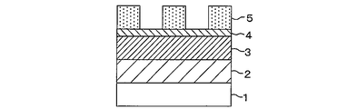
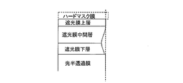
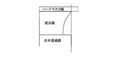
- FIG. 1 is a schematic cross-sectional view of an embodiment of a mask blank according to the present invention. It is a cross-sectional schematic diagram of the mask blank etc. which show the manufacturing process of the transfer mask using the mask blank which concerns on this invention. It is a cross-sectional schematic diagram of the mask blank etc. which show the manufacturing process of the transfer mask using the mask blank which concerns on this invention. It is a cross-sectional schematic diagram of the mask blank etc. which show the manufacturing process of the transfer mask using the mask blank which concerns on this invention. It is a cross-sectional schematic diagram of the mask blank etc. which show the manufacturing process of the transfer mask using the mask blank which concerns on this invention. It is a cross-sectional schematic diagram of the mask blank etc. which show the manufacturing process of the transfer mask using the mask blank which concerns on this invention. It is a cross-sectional schematic diagram of the mask blank etc.
- the inventor of the present invention has a predetermined laminated structure in the mask blank having a structure in which a light semi-transmissive film, a light shielding film, and a hard mask film are sequentially laminated on a light transmissive substrate.
- a predetermined laminated structure in the mask blank having a structure in which a light semi-transmissive film, a light shielding film, and a hard mask film are sequentially laminated on a light transmissive substrate.
- the present invention is a mask blank having a structure in which a light semi-transmissive film, a light-shielding film, and a hard mask film are sequentially laminated on a light-transmitting substrate as in the above-described configuration 1, and the light semi-transmissive film Contains at least silicon, the hard mask film contains at least one or both of silicon and tantalum, and the light shielding film has a laminated structure of a lower layer, an intermediate layer, and an upper layer,
- the mask blank is characterized in that it contains chromium, and the etching rate of dry etching using a mixed gas of chlorine gas and oxygen gas in the light-shielding film is the slowest in the upper layer and the slowest in the lower layer. .
- FIG. 1 is a schematic sectional view showing an embodiment of a mask blank according to the present invention.
- an embodiment 10 of a mask blank according to the present invention has a structure in which a light semi-transmissive film 2, a light shielding film 3, and a hard mask film 4 are sequentially laminated on a translucent substrate 1.
- the light shielding film 3 has a laminated structure of a lower layer 31, an intermediate layer 32, and an upper layer 33.
- the light translucent film 2 contains at least silicon
- the hard mask film 4 contains at least one or both of silicon and tantalum
- 3 contains chromium.
- the translucent substrate 1 in the mask blank 10 is not particularly limited as long as it is a substrate used for a transfer mask for manufacturing a semiconductor device.
- a synthetic quartz substrate or other various glass substrates for example, soda lime glass, alumino Silicate glass or the like.
- a synthetic quartz substrate is particularly preferably used because it is highly transparent in an ArF excimer laser (wavelength 193 nm) effective for fine pattern formation or in a shorter wavelength region.
- the hard mask film 4 can be made of a material containing silicon (Si) or a material containing tantalum (Ta).
- a material containing silicon (Si) suitable for the hard mask film 4 is selected from silicon (Si), oxygen (O), nitrogen (N), carbon (C), boron (B), and hydrogen (H). And a material containing one or more elements.
- silicon (Si) and transition metals include oxygen (O), nitrogen (N), carbon (C), boron (B And a material containing one or more elements selected from hydrogen (H).
- transition metal examples include molybdenum (Mo), tungsten (W), titanium (Ti), tantalum (Ta), zirconium (Zr), hafnium (Hf), niobium (Nb), vanadium (V), Examples include cobalt (Co), chromium (Cr), nickel (Ni), ruthenium (Ru), and tin (Sn).
- suitable materials containing tantalum (Ta) for the hard mask film 4 include tantalum (Ta), oxygen (O), nitrogen (N), carbon (C), boron (B), and hydrogen (H).
- Specific examples of such materials include tantalum oxide (TaO), tantalum oxynitride (TaON), tantalum boride oxide (TaBO), and tantalum boride oxynitride (TaBON).
- the hard mask film 4 is preferably formed of a material containing oxygen (O) in addition to silicon (Si) and tantalum (Ta). Such a hard mask film 4 has sufficient etching selectivity with respect to the light shielding film 3 formed of a material containing chromium (Cr), and the hard mask film 4 is hard without causing any damage to the light shielding film 3.
- the mask film 4 can be removed by etching.
- the material constituting the hard mask film 4 include silicon oxide (SiO 2 ), silicon oxynitride (SiON), tantalum oxide (TaO), tantalum oxynitride (TaON), and tantalum boride oxide (TaBO). And tantalum boride oxynitride (TaBON). Since the hard mask film 4 formed of a material containing silicon and oxygen tends to have low adhesion to a resist film made of an organic material, the surface of the hard mask film 4 is subjected to HMDS (Hexamethyldisilazane) treatment. It is preferable to improve surface adhesion.
- HMDS Hexamethyldisilazane
- the film thickness of the hard mask film 4 need not be particularly limited, but it needs to be a film thickness that does not disappear at least before the etching of the light shielding film 3 immediately below is completed. On the other hand, if the hard mask film 4 is thick, it is difficult to reduce the thickness of the resist pattern immediately above. From this point of view, in the present embodiment, the thickness of the hard mask film 4 is preferably in the range of 1.5 nm to 20 nm, particularly preferably 2.5 nm to 6 nm. is there.
- the light semi-transmissive film 2 is formed of a material containing at least silicon, but the configuration of the light semi-transmissive film 2 applicable to the present invention is not particularly limited, and has been conventionally used, for example.
- the configuration of the light semitransmissive film in the phase shift mask can be applied.
- Examples of such a light semi-transmissive film 2 include a metal silicide made of, for example, a transition metal and silicon, or a metal made of a material containing at least one element selected from oxygen, nitrogen, and carbon in the transition metal and silicon.
- Preferred examples include a silicide-based light semi-transmissive film and a silicon-based light semi-transmissive film made of a material containing silicon containing oxygen, nitrogen, carbon, boron, or the like.
- transition metal contained in the metal silicide light semi-transmissive film examples include molybdenum, tantalum, tungsten, titanium, chromium, nickel, vanadium, zirconium, ruthenium, and rhodium. Of these, molybdenum is particularly preferred.
- the material containing the transition metal and silicon specifically, a material containing transition metal silicide or transition metal silicide nitride, oxide, carbide, oxynitride, carbonate, or carbonitride is preferable. It is. Specific examples of the silicon-containing material include silicon nitride, oxide, carbide, oxynitride (oxynitride), carbonate (carbonized oxide), and carbonitride (carbonized and oxidized). A material containing (nitride) is preferable.
- the light semi-transmissive film 2 can be applied to either a single layer structure or a laminated structure including a low transmittance layer and a high transmittance layer.
- the preferable film thickness of the light semi-transmissive film 2 varies depending on the material, it is desirable to adjust appropriately from the viewpoint of the phase shift function and the light transmittance. Usually, it is suitable that the thickness is 100 nm or less, more preferably 80 nm or less.
- the light-shielding film 3 having the laminated structure is formed of a material containing chromium.
- the chromium-containing material include Cr compounds such as Cr alone or CrX (where X is at least one selected from N, C, O, etc.) (for example, CrN, CrC, CrO, CrON, CrCN, CrOC, CrOCN etc.).
- the sputtering film forming method is preferred.
- the sputtering film forming method is preferable because a uniform film having a constant film thickness can be formed.
- the light shielding film 3 has a laminated structure of the lower layer 31, the intermediate layer 32, and the upper layer 33, and contains chromium.
- the etching rate of dry etching using a mixed gas of chlorine gas and oxygen gas in the film 3 is characterized in that the upper layer 33 is the slowest and then the lower layer 31 is slow.
- the upper layer 33 of the light-shielding film 3 containing chromium immediately below the hard mask film 4 has an etching rate of dry etching using a mixed gas of chlorine gas and oxygen gas (hereinafter simply “etching rate”, it means the etching rate of dry etching using a mixed gas of chlorine gas and oxygen gas.
- Etch hardly occurs (in other words, the side wall of the pattern is not easily eroded). Since side etching is unlikely to occur in the upper layer 33 portion of the light shielding film 3, the pattern shape of the hard mask film 4 immediately above is transferred to the upper layer 33 of the light shielding film 3 almost accurately.
- the resist pattern having the transfer pattern to be finally formed on the light semi-transmissive film 2 is accurately transferred to the hard mask film 4. Since the light shielding film 3 has the upper layer 33 to which the pattern shape of the hard mask film 4 is transferred almost accurately and has a very small difference from the pattern shape (for example, pattern dimensions) formed on the resist film, the light shielding film 3
- the pattern of the hard mask film 4 can also be formed almost accurately on the silicon-containing semi-transmissive film 2 patterned by anisotropic etching using the pattern as a mask. In short, since the pattern of the light semi-transmissive film 2 can be formed without a difference in size from the resist pattern or the hard mask film pattern, the pattern accuracy formed on the light semi-transmissive film 2 can be increased.
- the intermediate layer 32 preferably has a thickness of 30% to 70%, more preferably 50% to 60%, with respect to the total thickness of the light shielding film 3. If the film thickness of the intermediate layer 32 is too thin, the effect of accelerating the etching rate of the entire light shielding film 3 is reduced. If the film thickness is too thick, the side etch in the intermediate layer 32 becomes too deep and the pattern in the lower layer 31 is reduced. There is a risk that shape recovery will be insufficient.
- the lower layer 31 having the slow etching rate after the upper layer 33 has a slower etching rate than the intermediate layer 32, side etching is less likely to occur than the intermediate layer 32 (the side walls of the pattern are less likely to be eroded). For this reason, in the etching process of the lower layer 31, excessive erosion of the side wall due to side etching is suppressed, so that the pattern shape of the upper layer 33 can be recovered, and the contact area between the pattern of the light shielding film 3 and the light semitransmissive film 2 is shielded. It can be secured in the lower layer 31 of the film 3. As a result, for example, when a pattern having a dimension of 50 nm or less is formed, the light shielding film pattern does not fall down.
- the light shielding film 3 is provided for the purpose of transferring the pattern of the hard mask film 4 to the light semi-transmissive film 2 as faithfully as possible.
- the final transfer pattern is a pattern formed on the light semi-transmissive film 2, and a pattern formed on the light shielding film 3. Since the pattern does not become a transfer pattern, the cross-sectional shape of the light shielding film pattern itself is not so important.
- the light shielding film 3 of the laminated structure of the present invention has the pattern of the hard mask film 4 as described above. Can be transferred to the light semi-transmissive film 2 as faithfully as possible, and there is no problem of the cross-sectional shape of the light-shielding film 3.
- the method for adjusting the etching rate of each layer of the light-shielding film 3 is not particularly limited, but it is preferable for the present invention to perform by changing the composition of each layer constituting the light-shielding film 3. Basically, it is possible by adjusting the chromium content of each layer, but for example, adjusting the degree of oxidation or nitridation of chromium in each layer, or making the composition other than chromium different in the composition of each layer You can adjust it. Further, the etching rate of each layer may be adjusted by adjusting the amount of an element (for example, indium or molybdenum) that can increase the etching rate.
- an element for example, indium or molybdenum
- the content of chromium is the highest in the upper layer 33 and the second highest in the lower layer 31 (Invention of Configuration 2). Since the upper layer 33 has a region with the highest chromium content in the light shielding film 3, the upper layer 33 has the slowest etching rate of dry etching using a mixed gas of chlorine gas and oxygen gas in the light shielding film 3. Become. Therefore, there is little side etching in the upper layer 33, and the pattern shape of the hard mask film 4 immediately above is almost accurately transferred to the upper layer 33 of the light shielding film 3, so that the transfer mask having an excellent pattern shape is finally obtained. Can be manufactured. Further, the upper layer 33 having the highest chromium content has an effect of increasing the optical density of the entire light shielding film 3 because of its high extinction coefficient.
- the lower layer 31 has the second largest chromium content after the upper layer 33, the adhesion to the light semi-transmissive film 2 having a film quality different from that of the light shielding film 3 is improved, so that the light shielding film pattern is more effectively tilted. Can be suppressed. That is, since the lower layer 31 has a relatively high chromium content, the number of vacant (holes) in the chromium binding site is relatively large, and therefore the adhesion with the light semi-transmissive film 2 of different film quality is improved. In addition, the fall of the light shielding film pattern can be more effectively suppressed.
- the surface of the light semi-transmissive film is in an oxygen-rich state. Since the vacant site of chromium and oxygen in the light-semitransmissive film are bonded with a chemical bond, the adhesion is improved. Since the intermediate layer 32 has a film configuration with the smallest chromium content in the light shielding film 3, the side wall portion of the pattern is eroded during etching, but the light shielding film 3 has such an intermediate layer 32. The etching rate as a whole can be increased.
- the upper layer 33 preferably has a chromium content of 60 atomic% or more (invention of Configuration 4).
- the chromium content of the upper layer 33 of the light shielding film 3 is 60 atomic% or more, the optical density of the entire light shielding film 3 can be increased by the upper layer 33, the etching rate in the upper layer 33 is slowed down, and side etching in the upper layer portion is performed. Therefore, the pattern shape of the hard mask film 4 directly above is transferred almost accurately, and finally a transfer mask having an excellent pattern shape can be manufactured.
- the oxygen content is preferably lower in the lower layer 31 than in the intermediate layer 32 (Invention of Configuration 3). Since the oxygen content in the light-shielding film 3 is lower in the lower layer 31 than in the intermediate layer 32, the oxygen content in the intermediate layer 32 is the highest, so that the etching rate of the intermediate layer 32 is faster. For this reason, the etching rate of the whole light shielding film 3 can be kept fast. In addition, since the oxygen content contained in the lower layer 31 is lower than that in the intermediate layer 32, the etching rate in the depth direction is slowed when etching is transferred from the intermediate layer 32 to the lower layer 31.
- the pattern shape of the upper layer 33 is restored in the lower layer 31 and the dimension in the width direction of the pattern is maintained.
- the contact area between the pattern of the light shielding film 3 and the light semi-transmissive film 2 is maintained. Can do.
- the oxygen content of the lower layer 31 is relatively small, the light translucent film 2 is exchanged with oxygen and bonded with a chemical bond, so that the pattern of the light shielding film 3 and the light semitransmissive film 2 The effect of further improving the adhesiveness is also obtained.
- the upper layer 33 preferably has a thickness of 3 nm or more and 8 nm or less (Invention of Configuration 5). If the thickness of the upper layer 33 is less than 3 nm, the risk of erosion of the pattern side wall of the upper layer 33 during dry etching increases, and if the thickness of the upper layer 33 exceeds 8 nm, the etching time of the upper layer 33 may be increased. Occurs. Therefore, by setting the thickness of the upper layer 33 of the light shielding film 3 in the range of 3 nm or more and 8 nm or less, the etching time of the upper layer 33 is suitably suppressed, and the patterning accuracy in the upper layer 33 is favorably maintained. Can do.
- the etching rate of dry etching using a mixed gas of chlorine gas and oxygen gas in the light shielding film 3 is characterized in that the upper layer 33 is the slowest and then the lower layer 31 is slow. Therefore, the intermediate layer 32 has the fastest etching rate.
- the etching rate of the light shielding film 3 in the intermediate layer 32 is preferably at least three times the etching rate of the upper layer 33 (Invention of Configuration 6).
- the etching rate in the intermediate layer 32 is three times or more than the etching rate in the upper layer 33, the etching rate in the depth direction is increased when etching is transferred from the upper layer 33 to the intermediate layer 32. It is preferable because etching in the depth direction of the intermediate layer 32 can be completed while suppressing the progress of side etching at 33.
- the etching rate in the intermediate layer 32 is preferably not more than twice the etching rate in the lower layer 31 (Invention of Configuration 7).
- the etching rate in the depth direction becomes slow.
- the etching rate in the intermediate layer 32 is less than or equal to twice the etching rate in the lower layer 31.
- the hard mask film 4 contains at least one or both of silicon and tantalum, but is preferably formed of a material containing oxygen in addition to silicon or tantalum ( Invention of Configuration 8).
- the hard mask film 4 is required to be a material having high etching selectivity with respect to the light shielding film 3 directly below.
- the hard mask film 4 is made of a material containing silicon and oxygen or a material containing tantalum and oxygen.
- the light semi-transmissive film 2 contains at least silicon, but is preferably formed of a material containing silicon and nitrogen in particular (Invention of Configuration 9).
- a material containing silicon and nitrogen By applying a material containing silicon and nitrogen to the light semi-transmissive film 2, etching selectivity with the chromium-based light-shielding film 3 can be ensured.
- the material contains silicon and nitrogen, patterning using an anisotropic fluorine-based gas as an etching gas can be applied. Therefore, a transfer pattern having excellent pattern accuracy can be formed also in the light semi-transmissive film 2 by anisotropic etching using the pattern of the light shielding film 3 to which the pattern shape of the hard mask film 4 is transferred almost accurately. .
- the transmittance for ArF excimer laser light (wavelength 193 nm) in the laminated structure of the light semi-transmissive film 2 and the light-shielding film 3 is 0.2% or less, and 800 to It is preferable that the light transmittance in at least a part of the wavelength region of 900 nm is 50% or less (Invention of Configuration 10).
- Light in the near-infrared region with a wavelength of 800 to 900 nm is light used for positioning when a mask blank is placed on an exposure machine because the resist is not exposed.
- the transmittance for ArF excimer laser light (wavelength 193 nm) in the laminated structure of the light semi-transmissive film 2 and the light shielding film 3 is 0.2% or less and at least one in the wavelength region of 800 to 900 nm. Since the light transmittance at the wavelength of the portion is 50% or less, for example, it has a good light shielding property against the ArF excimer laser of the exposure light required for the light shielding band, and the mask blank can be easily arranged on the exposure machine. Therefore, it is preferable.
- the hard mask film 4 and the light semi-transmissive film 2 can be patterned by dry etching using a fluorine-based gas. Combined with the fact that the pattern shape of the hard mask film 4 just above is transferred almost accurately, the pattern shape accuracy is excellent in the light semi-transmissive film 2 by patterning by anisotropic etching using the light shielding film 3 as a mask. A transfer pattern can be formed.
- the present invention also provides a method for manufacturing a transfer mask using the mask blank according to the present invention.
- 2A to 2E are schematic cross-sectional views of a mask blank and the like showing a manufacturing process of a transfer mask using the mask blank 10 according to the embodiment of the present invention.
- 2A to 2E are for facilitating understanding of the manufacturing process, and the cross-sectional shapes of the patterns shown in FIGS. 2A to 2E do not accurately represent the cross-sectional shapes actually formed.
- a predetermined resist pattern 5 is formed on the surface of the mask blank 10 (see FIG. 2A).
- This resist pattern 5 has a desired pattern to be formed on the light semi-transmissive film 2 which becomes a final transfer pattern.
- the resist pattern 5 having the light semi-transmissive film pattern formed on the hard mask film 4 of the mask blank 10 as a mask the light mask is formed on the hard mask film 4 by dry etching using a fluorine-based gas.
- a hard mask film pattern 4a corresponding to the pattern of the permeable film is formed (see FIG. 2B).
- the light shielding film 3 having a laminated structure corresponds to the pattern of the light semi-transmissive film by dry etching using a mixed gas of chlorine gas and oxygen gas.
- a light shielding film pattern 3a is formed (see FIG. 2C).
- the light semi-transmissive film pattern 2a is formed on the light semi-transmissive film 2 by dry etching using a fluorine-based gas using the light shielding film pattern 3a formed as described above as a mask (see FIG. 2D). In the etching process of the light semitransmissive film 2, the hard mask film pattern 4a exposed on the surface is removed.
- a resist film is applied to the entire surface of the light shielding film pattern 3a, and a resist pattern (not shown) corresponding to a light shielding pattern (for example, a light shielding band pattern) formed on the light shielding film is formed by predetermined exposure and development processes. .
- a predetermined light shielding pattern 3b is formed on the light semi-transmissive film pattern 2a by dry etching using a mixed gas of chlorine gas and oxygen gas.
- a transfer mask for example, a halftone phase shift mask
- a transfer mask is manufactured according to the manufacturing process using the mask blank 10 according to the embodiment of the present invention, so that even a fine pattern such as an SRAF pattern is a high pattern.
- a transfer mask formed with high accuracy can be obtained. That is, according to the mask blank 10 according to the embodiment of the present invention, since the etching rate of the upper layer 33 of the light shielding film 3 is the slowest and the side etching of the upper layer pattern is small, the transfer pattern formed on the resist film or the hard mask film 4 Since the pattern of the light shielding film 3 having the shape transferred almost accurately can be formed, the pattern accuracy to be formed on the light semi-transmissive film 2 can be increased using the light shielding film pattern as a mask.
- the etching rate of the lower layer 31 of the light shielding film 3 is the second slower than that of the upper layer 33 and is slower than that of the intermediate layer 32, and the side etching of the lower layer pattern can be reduced. A sufficient contact area can be ensured and good adhesion can be obtained. Therefore, even if a fine pattern such as an SRAF pattern is formed, the light shielding film pattern does not fall down, so that the pattern of the light semi-transmissive film 2 can also be formed with high pattern accuracy.
- the transfer pattern of the transfer mask is formed by a lithography method. According to the method for manufacturing a semiconductor device including the step of transferring the pattern onto the substrate, a high-quality semiconductor device with excellent pattern accuracy can be obtained.
- Example 1 The present embodiment relates to a mask blank used for manufacturing a halftone phase shift mask using an ArF excimer laser having a wavelength of 193 nm as exposure light.
- the mask blank used in this example is as shown in FIG. 1.
- a translucent substrate (glass substrate) 1 On a translucent substrate (glass substrate) 1, a light semi-transmissive film 2, a light shielding film 3 having a three-layer structure, and a hard mask film 4 are sequentially formed. It has a laminated structure.
- This mask blank was produced as follows.
- a synthetic quartz substrate (size: about 152 mm ⁇ 152 mm ⁇ thickness 6.35 mm) was prepared as a glass substrate.
- a MoSiN light semi-transmissive film made of molybdenum, silicon, and nitrogen was formed to a thickness of 69 nm on the synthetic quartz substrate.
- the substrate was taken out from the sputtering apparatus, and the light semi-transmissive film on the synthetic quartz substrate was subjected to heat treatment in the atmosphere. This heat treatment was performed at 450 ° C. for 30 minutes.
- the transmittance and the phase shift amount at the wavelength (193 nm) of the ArF excimer laser were measured for the light-semitransmissive film after the heat treatment using a phase shift amount measuring device, the transmittance was 6.44% and the phase The shift amount was 174.3 degrees.
- the substrate on which the light semi-transmissive film is formed is again put into the sputtering apparatus, and on the light semi-transmissive film, a lower layer made of a CrOCN film, an intermediate layer made of a CrOCN film, and an upper layer made of a CrN film.
- a light shielding film having a laminated structure was formed.
- argon Ar
- CO 2 carbon dioxide
- N 2 nitrogen
- He helium
- a light shielding film lower layer made of a CrOCN film having a thickness of 15.4 nm was formed on the light semi-transmissive film.
- a light-shielding film intermediate layer made of a CrOCN film having a thickness of 26.6 nm is formed on the lower layer by reactive sputtering.
- a hard mask film made of a SiON film was formed on the light shielding film.
- Ar argon
- NO nitric oxide
- He helium
- a hard mask film made of a SiON film having a thickness of 15 nm was formed on the light shielding film by performing reactive sputtering.
- the optical density of the laminated film of the light semi-transmissive film and the light shielding film was 3.0 or more (transmittance of 0.1% or less) at the wavelength (193 nm) of the ArF excimer laser. Further, the transmittance at a wavelength of 880 nm (a wavelength used for positioning a substrate mounted on the exposure apparatus) was 50% or less.
- a mask blank of this example was produced as described above.
- a halftone phase shift mask was manufactured according to the manufacturing process shown in FIGS. 2A to 2E.
- the following reference numerals correspond to those in FIG. 1 and FIGS. 2A to 2E.
- an HMDS process is performed on the upper surface of the mask blank 10
- a chemical amplification resist for electron beam drawing PRL009 manufactured by Fuji Film Electronics Materials
- PRL009 manufactured by Fuji Film Electronics Materials
- the hard mask film 4 was dry-etched to form a hard mask film pattern 4a (see FIG. 2B).
- a fluorine-based gas (SF 6 ) was used as the dry etching gas.
- the light shielding film 3 composed of an upper layer, an intermediate layer, and a lower layer was continuously dry-etched using the hard mask film pattern 4 a as a mask to form a light shielding film pattern 3 a ( (See FIG. 2C).
- the etching rate of the light shielding film 3 was 2.9 ⁇ / sec for the upper layer, 9.1 ⁇ / sec for the intermediate layer, and 5.1 ⁇ / sec for the lower layer.
- the light semi-transmissive film 2 was dry-etched to form a light semi-transmissive film pattern 2a (phase shift film pattern) (see FIG. 2D).
- a fluorine-based gas (SF 6 ) was used as the dry etching gas.
- the hard mask film pattern 4a exposed on the surface was removed.
- the resist film is formed again on the entire surface of the substrate in the state shown in FIG. 2D by spin coating, and a predetermined device pattern (for example, a pattern corresponding to a light-shielding band pattern) is formed using an electron beam drawing machine. After drawing, development was performed to form a predetermined resist pattern. Subsequently, by using this resist pattern as a mask, the exposed light shielding film pattern 3a is etched to remove, for example, the light shielding film pattern 3a in the transfer pattern formation region, and light shielding is applied to the periphery of the transfer pattern formation region. A band pattern 3b was formed.
- a predetermined device pattern for example, a pattern corresponding to a light-shielding band pattern
- the light semi-transmissive film and the hard mask film were the same as those in Example 1, and different mask blanks were produced. That is, the light-shielding film of this comparative example is a light-shielding film having a single-layer structure, and is a thin film having the same composition as the intermediate layer in the light-shielding film of Example 1, an optical density of 3.0 or more, and a film thickness of 100 nm. .
- a halftone phase shift mask was produced in the same manner as in Example 1.
- the pattern dimension was increased by 10 nm and the state of the light shielding film pattern was confirmed, it was 80 nm line and space that the pattern did not collapse. This is because the wall surface of the light-shielding film pattern is greatly eroded, the contact area between the light-shielding film and the light semi-transmissive film is narrow, and the bonding state (adhesion state) that can withstand cleaning at the interface between the light shielding film and the light semi-transmissive film This is thought to be due to the failure to secure this.
Landscapes
- Physics & Mathematics (AREA)
- General Physics & Mathematics (AREA)
- Preparing Plates And Mask In Photomechanical Process (AREA)
- Chemical & Material Sciences (AREA)
- Chemical Kinetics & Catalysis (AREA)
- General Chemical & Material Sciences (AREA)
Abstract
Description
以上のように、従来構成のマスクブランクを用いて、例えばSRAFパターンのような微細なパターンを転写用マスク膜に形成しようとする場合、高いパターン精度を得ることが困難である。
すなわち、上記課題を解決するため、本発明は以下の構成を有する。
透光性基板上に、光半透過膜、遮光膜及びハードマスク膜が順に積層された構造を有するマスクブランクであって、前記光半透過膜は、少なくともケイ素を含有しており、前記ハードマスク膜は、少なくともケイ素とタンタルのいずれか一方または両方を含有しており、前記遮光膜は、下層、中間層及び上層の積層構造であって、クロムを含有しており、前記遮光膜における塩素ガスと酸素ガスの混合ガスを用いたドライエッチングのエッチングレートは、前記上層が最も遅く、次いで前記下層が遅い、ことを特徴とするマスクブランク。
構成1によれば、ハードマスク膜の直下にあるクロムを含有する遮光膜の上層は、塩素ガスと酸素ガスの混合ガスを用いたドライエッチングのエッチングレートが遮光膜の中で最も遅いため、エッチング中のサイドエッチが生じにくい(パターンの側壁が侵食されにくい)。遮光膜の上層のサイドエッチが生じにくいことで、遮光膜の上層には、直上のハードマスク膜のパターン形状がほぼ正確に転写される。ハードマスク膜のパターン形状がほぼ正確に転写された上層を遮光膜が有することで、遮光膜のパターンをマスクとしてパターニングされるケイ素含有の光半透過膜にも、ハードマスク膜のパターンをほぼ正確に形成することができる。
また、上層に次いでエッチングレートの遅い下層は、中間層よりもエッチングレートが遅いため、中間層よりもサイドエッチが生じにくい(パターンの側壁が侵食されにくい)。このため、下層のエッチング過程ではサイドエッチによる側壁の過度な侵食が抑制されるため、遮光膜パターンと光半透過膜との接触面積を遮光膜の下層で確保することができる。その結果、たとえば寸法が50nm以下のパターンを形成する場合も、遮光膜パターンが倒れてしまうことはない。
以上のように、構成1によれば、SRAFパターンのような微細な転写パターンであっても、本発明のマスクブランクの転写用マスク膜となる光半透過膜に高精度で形成することができ、結果、パターン精度に優れた転写用マスクを製造することができる。
前記遮光膜において、クロムの含有量は、前記上層が最も多く、前記下層が次に多い、ことを特徴とする構成1に記載のマスクブランク。
構成2のように、遮光膜の上層部分にクロムの含有量が最も多い領域を有することで、上層が、塩素ガスと酸素ガスの混合ガスを用いたドライエッチングのエッチングレートが遮光膜の中で最も遅くなり、上記のとおり、遮光膜の上層には、直上のハードマスク膜のパターン形状がほぼ正確に転写されるため、最終的にはパターン形状に優れた転写用マスクを製造することができる。また、下層は、上層に次いでクロムの含有量が多いため、遮光膜とは異なる膜質の光半透過膜との密着性も良くなるので、遮光膜パターンの倒れをより効果的に抑制することができる。なお、中間層は、クロムの含有量が最も少ないため、エッチング時にパターンの側壁部分の侵食はあるものの、このような中間層を有することで遮光膜全体としてのエッチングレートを速めることができる。
前記遮光膜にはさらに酸素が含まれており、酸素の含有量は、前記中間層よりも前記下層のほうが少ないことを特徴とする構成1又は2に記載のマスクブランク。
構成3のように、遮光膜中の酸素の含有量は、中間層よりも下層のほうが少ないことにより、中間層の酸素含有量が最も多くなるため、中間層のエッチングレートがより速くなる。このため、遮光膜全体のエッチングレートを速く保つことができる。また、下層に含まれる酸素含有量が中間層よりも少ないことで、中間層から下層にエッチングが移行するときに深さ方向のエッチングレートが遅くなるが、下層におけるパターンのサイドエッチの進行も遅くなるため、下層でパターンの幅方向の寸法が保たれ、結果、遮光膜のパターンと光半透過膜との接触面積を保つことができる。さらに、下層の酸素含有量が相対的に少ないことによって遮光膜パターンと光半透過膜との密着性をより高める効果も得られる。
前記上層は、クロムの含有量が60原子%以上であることを特徴とする構成1乃至3のいずれかに記載のマスクブランク。
構成4のように、遮光膜の上層のクロム含有量が60原子%以上であることにより、上層によって遮光膜全体の光学濃度を高められるとともに、上層におけるドライエッチングのエッチングレートが遅くなり、上層部分でのサイドエッチが抑制されるので、直上のハードマスク膜のパターン形状がほぼ正確に転写され、最終的にはパターン形状に優れた転写用マスクを製造することができる。
前記上層は、厚さが3nm以上8nm以下であることを特徴とする構成1乃至4のいずれかに記載のマスクブランク。
構成5のように、遮光膜の上層の厚さを3nm以上8nm以下の範囲とすることにより、上層のエッチング時間を好適に抑制しつつ、上層でのパターニング精度を良好に維持することができる。
前記中間層における塩素ガスと酸素ガスの混合ガスを用いたドライエッチングのエッチングレートは、前記上層における塩素ガスと酸素ガスの混合ガスを用いたドライエッチングのエッチングレートの3倍以上であることを特徴とする構成1乃至5のいずれかに記載のマスクブランク。
構成6にあるように、中間層における塩素ガスと酸素ガスの混合ガスを用いたドライエッチングのエッチングレートが、上層におけるエッチングレートの3倍以上であることにより、上層から中間層にエッチングが移行するときに深さ方向のエッチングレートが速まり、上層でのサイドエッチの進行を抑制しつつ中間層の深さ方向のエッチングを完結することができる。
前記中間層における塩素ガスと酸素ガスの混合ガスを用いたドライエッチングのエッチングレートは、前記下層における塩素ガスと酸素ガスの混合ガスを用いたドライエッチングのエッチングレートの2倍以下であることを特徴とする構成1乃至6のいずれかに記載のマスクブランク。
構成1のように中間層から下層にエッチングが移行するときに深さ方向のエッチングレートが遅くなるが、構成7にあるように、中間層におけるエッチングレートが下層におけるエッチングレートの2倍以下であることにより、下層のエッチング時に、中間層のサイドエッチがより進行する前に下層のエッチング及び必要なオーバーエッチングが完了するため、とくにパターン側壁の中間層と下層との界面での段差形成を抑制することができる。
前記ハードマスク膜は、酸素を含有することを特徴とする構成1乃至7のいずれかに記載のマスクブランク。
ハードマスク膜は、直下の遮光膜とエッチング選択性の高い素材であることが必要であるが、構成8にあるように、ハードマスク膜にケイ素やタンタルの酸化物等を含有する素材を選択することにより、クロム系の素材からなる遮光膜との高いエッチング選択性を確保することができ、レジストの薄膜化のみならずハードマスク膜の膜厚も薄くすることが可能である。したがって、マスクブランク表面に形成されたレジストパターンの転写精度が向上する。
前記光半透過膜は、ケイ素と窒素を含有することを特徴とする構成1乃至8のいずれかに記載のマスクブランク。
構成9にあるように、光半透過膜にケイ素と窒素を含有する素材を適用することで、クロム系の遮光膜とのエッチング選択性を確保することができる。また、ケイ素と窒素を含有する素材であれば、エッチングガスとして異方性のフッ素系ガスを使用したパターニングを適用することができる。したがって、ハードマスク膜のパターン形状がほぼ正確に転写された遮光膜パターンをマスクとすることによって光半透過膜にもパターン精度に優れたパターンを形成することができる。
前記光半透過膜と前記遮光膜の積層構造におけるArFエキシマレーザー光(波長193nm)に対する透過率が0.2%以下であり、かつ、800~900nmの波長領域の少なくとも一部の波長における光の透過率が50%以下であることを特徴とする構成1乃至9のいずれかに記載のマスクブランク。
波長800~900nmの近赤外領域の光はレジストを感光しないため、露光機にマスクブランクを配置する場合の位置決めに使用される光である。構成10にあるように、光半透過膜と遮光膜の積層構造におけるArFエキシマレーザー光(波長193nm)に対する透過率が0.2%以下であり、かつ、800~900nmの波長領域の少なくとも一部の波長における光の透過率が50%以下であることによって、露光光のArFエキシマレーザーに対する良好な遮光性を備え、かつ、露光機へのマスクブランクの配置が容易になるため好ましい。
前記ハードマスク膜および光半透過膜は、フッ素系ガスを用いたドライエッチングによってパターニングされることを特徴とする構成1乃至10のいずれかに記載のマスクブランク。
構成11によれば、ハードマスク膜および光半透過膜は、異方性のフッ素系ガスを用いたドライエッチングによってパターニングされるので、遮光膜の上層に直上のハードマスク膜のパターン形状がほぼ正確に転写されることと相俟って、該遮光膜をマスクとするパターニングにより光半透過膜にパターン形状精度に優れた転写パターンを形成することができる。
構成1乃至11のいずれかに記載のマスクブランクを用いる転写用マスクの製造方法であって、前記ハードマスク膜上に形成された光半透過膜のパターンを有するレジスト膜をマスクとし、フッ素系ガスを用いたドライエッチングにより、前記ハードマスク膜に光半透過膜のパターンを形成する工程と、前記光半透過膜のパターンが形成されたハードマスク膜をマスクとし、塩素ガスと酸素ガスの混合ガスを用いたドライエッチングにより、前記遮光膜に光半透過膜のパターンを形成する工程と、前記光半透過膜のパターンが形成された遮光膜をマスクとし、フッ素系ガスを用いたドライエッチングにより、前記光半透過膜に光半透過膜のパターンを形成する工程と、前記遮光膜上に形成された遮光パターンを有するレジスト膜をマスクとし、塩素ガスと酸素ガスの混合ガスを用いたドライエッチングにより、前記遮光膜に遮光パターンを形成する工程と、を有することを特徴とする転写用マスクの製造方法。
構成12にあるように、本発明に係るマスクブランクを用いて上記製造工程により転写用マスクを製造することによって、SRAFパターンのような微細パターンが高精度で形成された転写用マスクを得ることができる。
構成11に記載の転写用マスクの製造方法により製造された転写用マスクを用い、リソグラフィー法により前記転写用マスクの転写パターンを半導体基板上にパターン転写する工程を含むことを特徴とする半導体装置の製造方法。
構成13にあるように、上記の微細パターンが高精度で形成された転写用マスクを用いて、パターン精度の優れた高品質の半導体装置を得ることができる。
また、このような本発明のマスクブランクを用いることにより、微細パターンが高精度で形成された転写用マスクを製造することができる。
さらに、かかる転写用マスクを用いて、パターン精度の優れた高品質の半導体装置を製造することができる。
前述のように、本発明者は、透光性基板上に、光半透過膜、遮光膜及びハードマスク膜が順に積層された構造を有するマスクブランクにおいて、上記遮光膜を所定の積層構造とし、遮光膜の各層における塩素ガスと酸素ガスの混合ガスを用いたドライエッチングのエッチングレートに着目して鋭意検討した結果、以下の構成を有する本発明によって前記の課題を解決できることを見出したものである。
図1にあるとおり、本発明に係るマスクブランクの一実施の形態10は、透光性基板1上に、光半透過膜2、遮光膜3、及びハードマスク膜4が順に積層された構造を有する。また、上記遮光膜3は、下層31、中間層32、及び上層33の積層構造である。
なお、ケイ素と酸素を含有する材料で形成されたハードマスク膜4は、有機系材料のレジスト膜との密着性が低い傾向があるため、ハードマスク膜4の表面をHMDS(Hexamethyldisilazane)処理を施し、表面の密着性を向上させることが好ましい。
このような光半透過膜2の例としては、例えば遷移金属及びケイ素からなる金属シリサイド、あるいは遷移金属とケイ素に、酸素、窒素及び炭素から選ばれる1以上の元素を含有させた材料からなる金属シリサイド系の光半透過膜、ケイ素に酸素、窒素、炭素、ホウ素等を含有させた材料からなるケイ素系の光半透過膜が好ましく挙げられる。上記金属シリサイド系の光半透過膜に含まれる遷移金属としては、例えばモリブデン、タンタル、タングステン、チタン、クロム、ニッケル、バナジウム、ジルコニウム、ルテニウム、ロジウム等が挙げられる。この中でも特にモリブデンが好適である。
上記光半透過膜2の好ましい膜厚は、材質によっても異なるが、特に位相シフト機能、光透過率の観点から適宜調整されることが望ましい。通常は、100nm以下、さらに好ましくは80nm以下の範囲であることが好適である。
上記クロムを含有する材料としては、例えばCr単体、あるいはCrX(ここでXはN、C、O等から選ばれる少なくとも一種)などのCr化合物(例えばCrN,CrC,CrO,CrON,CrCN,CrOC,CrOCNなど)が挙げられる。
なお、遮光膜3の各層のエッチングレートの調整方法は特に限定されないが、遮光膜3を構成する各層の組成をそれぞれ異ならせることによって行うことが本発明には好適である。基本的には、各層のクロム含有量を調整することで可能であるが、例えば、各層で、クロムの酸化度や窒化度等を調整したり、各層の組成におけるクロム以外の構成を異ならせたりすることで調整することができる。また、エッチングレートを速めることができる元素(たとえばインジウムやモリブデン)の添加量を調整することによって各層のエッチングレートを調整するようにしてもよい。
遮光膜3の上層33部分にクロムの含有量が最も多い領域を有することで、上層33が、塩素ガスと酸素ガスの混合ガスを用いたドライエッチングのエッチングレートが遮光膜3の中で最も遅くなる。そのため、上層33でのサイドエッチが少なく、遮光膜3の上層33には、直上のハードマスク膜4のパターン形状がほぼ正確に転写されるため、最終的にはパターン形状に優れた転写用マスクを製造することができる。また、クロム含有量の最も多い上層33は、消衰係数が高いため遮光膜3全体の光学濃度を高める効果も有する。
なお、中間層32は、遮光膜3中でクロムの含有量が最も少ない膜構成となるため、エッチング時にパターンの側壁部分の侵食はあるものの、このような中間層32を有することで遮光膜3全体としてのエッチングレートを速めることができる。
遮光膜3の上層33のクロム含有量が60原子%以上であることにより、上層33によって遮光膜3全体の光学濃度を高められるとともに、上層33におけるエッチングレートが遅くなり、上層部分でのサイドエッチが抑制されるので、直上のハードマスク膜4のパターン形状がほぼ正確に転写され、最終的にはパターン形状に優れた転写用マスクを製造することができる。
遮光膜3中の酸素の含有量が、中間層32よりも下層31のほうが少ないことにより、中間層32の酸素含有量が最も多くなるため、中間層32のエッチングレートがより速くなる。このため、遮光膜3全体のエッチングレートを速く保つことができる。また、下層31に含まれる酸素含有量が中間層32よりも少ないことで、中間層32から下層31にエッチングが移行するときに深さ方向のエッチングレートが遅くなるが、下層31におけるパターンのサイドエッチの進行も遅くなるため、下層31で上層33のパターン形状が回復し、パターンの幅方向の寸法が保たれ、結果、遮光膜3のパターンと光半透過膜2との接触面積を保つことができる。さらに、下層31の酸素含有量が相対的に少ないことによって光半透過膜2の酸素とのやりとりが生じ、化学的結合を持って接合するため、遮光膜3のパターンと光半透過膜2との密着性をより高める効果も得られる。
上層33の厚さが3nmを下回ると、ドライエッチング時の上層33のパターン側壁の侵食のリスクが高くなる、また、上層33の厚さが8nmを超えると、上層33のエッチング時間が長くなる恐れが生じる。したがって、遮光膜3の上層33の厚さを、上記の3nm以上8nm以下の範囲とすることにより、上層33のエッチング時間を好適に抑制しつつ、上層33でのパターニング精度を良好に維持することができる。
このように、中間層32におけるエッチングレートが、上層33におけるエッチングレートの3倍以上であることにより、上層33から中間層32にエッチングが移行するときに深さ方向のエッチングレートが速まり、上層33でのサイドエッチの進行を抑制しつつ中間層32の深さ方向のエッチングを完結することができるので好ましい。
中間層32から下層31にエッチングが移行するときに深さ方向のエッチングレートが遅くなるが、このとき中間層32におけるエッチングレートが下層31におけるエッチングレートの2倍以下であることにより、下層31のエッチング時に、中間層32のサイドエッチがより進行する前に下層31のエッチング及び必要なオーバーエッチングが完了するため、とくにパターン側壁の中間層32と下層31との界面での段差形成を抑制することができる。
上記ハードマスク膜4は、直下の遮光膜3とエッチング選択性の高い素材であることが必要であるが、とくにハードマスク膜4にケイ素と酸素を含有する素材やタンタルと酸素を含有する素材を選択することにより、クロム系の素材からなる遮光膜3との高いエッチング選択性を確保することができるため、レジスト膜の薄膜化のみならずハードマスク膜4の膜厚も薄くすることが可能である。したがって、マスクブランク表面に形成された転写パターンを有するレジストパターンのハードマスク膜4への転写精度が向上する。
上記光半透過膜2にケイ素と窒素を含有する素材を適用することで、クロム系の遮光膜3とのエッチング選択性を確保することができる。また、ケイ素と窒素を含有する素材であれば、エッチングガスとして異方性のフッ素系ガスを使用したパターニングを適用することができる。したがって、ハードマスク膜4のパターン形状がほぼ正確に転写された遮光膜3のパターンをマスクとする異方性エッチングによって光半透過膜2にもパターン精度に優れた転写パターンを形成することができる。
波長800~900nmの近赤外領域の光はレジストを感光しないため、露光機にマスクブランクを配置する場合の位置決めに使用される光である。本構成のように、光半透過膜2と遮光膜3の積層構造におけるArFエキシマレーザー光(波長193nm)に対する透過率が0.2%以下であり、かつ、800~900nmの波長領域の少なくとも一部の波長における光の透過率が50%以下であることによって、たとえば遮光帯に要求される露光光のArFエキシマレーザーに対する良好な遮光性を備え、かつ、露光機へのマスクブランクの配置が容易になるため好ましい。
図2A~図2Eは、本発明の実施形態に係るマスクブランク10を用いた転写用マスクの製造工程を示すマスクブランク等の断面概略図である。なお、図2A~図2Eは製造工程の理解を容易にするためのものであり、図2A~図2Eに示すパターンの断面形状は実際に形成される断面形状を正確に現したものではない。
次に、マスクブランク10のハードマスク膜4上に形成された上記の光半透過膜のパターンを有するレジストパターン5をマスクとして、フッ素系ガスを用いたドライエッチングにより、ハードマスク膜4に光半透過膜のパターンに対応するハードマスク膜パターン4aを形成する(図2B参照)。
次に、上記のように形成された遮光膜パターン3aをマスクとして、フッ素系ガスを用いたドライエッチングにより、光半透過膜2に光半透過膜パターン2aを形成する(図2D参照)。なお、この光半透過膜2のエッチング工程において、表面に露出しているハードマスク膜パターン4aは除去される。
(実施例1)
本実施例は、波長193nmのArFエキシマレーザーを露光光として用いるハーフトーン型位相シフトマスクの製造に使用するマスクブランクに関する。
本実施例に使用するマスクブランクは、図1に示すような、透光性基板(ガラス基板)1上に、光半透過膜2、3層積層構造の遮光膜3、ハードマスク膜4を順に積層した構造のものである。このマスクブランクは、以下のようにして作製した。
次に、枚葉式DCスパッタリング装置内に上記合成石英基板を設置し、モリブデン(Mo)とシリコン(Si)との混合焼結ターゲット(Mo:Si=12原子%:88原子%)を用い、アルゴン(Ar)、窒素(N2)およびヘリウム(He)の混合ガス(流量比 Ar:N2:He=8:72:100,圧力=0.2Pa)をスパッタリングガスとし、反応性スパッタリング(DCスパッタリング)により、合成石英基板上に、モリブデン、シリコンおよび窒素からなるMoSiN光半透過膜(位相シフト膜)を69nmの厚さで形成した。形成したMoSiN膜の組成は、Mo:Si:N=4.1:35.6:60.3(原子%比)であった。この組成はXPSにより測定した。
以上のようにして本実施例のマスクブランクを作製した。
まず、上記マスクブランク10の上面にHMDS処理を行い、スピン塗布法によって、電子線描画用の化学増幅型レジスト(富士フィルムエレクトロニクスマテリアルズ社製 PRL009)を塗布し、所定のベーク処理を行って、膜厚150nmのレジスト膜を形成した。
上記レジストパターン5を除去した後、上記ハードマスク膜パターン4aをマスクとして、上層、中間層及び下層の積層膜からなる遮光膜3のドライエッチングを連続して行い、遮光膜パターン3aを形成した(図2C参照)。ドライエッチングガスとしてはCl2とO2の混合ガス(Cl2:O2=8:1(流量比))を用いた。なお、遮光膜3のエッチングレートは、上層が2.9Å/秒、中間層が9.1Å/秒、下層が5.1Å/秒であった。
最後に、残存するレジストパターンを除去し、ハーフトーン型位相シフトマスク20を作製した(図2E参照)。
上記の光半透過膜2のエッチング工程(図2Dの工程)終了後の遮光膜パターンの断面形状を確認したところ、図3に示されるような断面形状であった。すなわち遮光膜の中間層部分ではパターンの壁面にエッチングの侵食による括れがあるものの、下層部分でパターン幅が回復するような形状でパターニングされていた。なお、この時点でハードマスク膜パターン4aは除去されているため、図3ではその前の状態を破線で示している。
また、遮光膜3のパターニング工程(図2Cの工程)終了後に洗浄を行い、ラインアンドスペース40nm(SRAFパターンのパターン寸法に相当)のパターンの状態を確認したところ、遮光膜パターンに倒れは生じていなかった。これは、遮光膜下層と光半透過膜との接触面積が確保され、かつ、遮光膜下層と光半透過膜の界面での接合性が良好で、密着性が確保されたことによるものと考えられる。
上記遮光膜パターンをマスクとしたドライエッチングにより形成された光半透過膜パターンについて評価したところ、図3からも明らかなように、ラインアンドスペース40nmのような微細パターンであっても、ハードマスク膜パターンとの寸法の乖離も少ないパターン精度の優れた転写パターンを形成することができた。
光半透過膜とハードマスク膜は実施例1と同様の膜で、遮光膜の構成のみ異なるマスクブランクを作製した。すなわち、本比較例の遮光膜は、単層構造の遮光膜で、実施例1の遮光膜における中間層の組成と同じ組成で、光学濃度が3.0以上で、膜厚100nmの薄膜である。
この比較例のマスクブランクを用いて、実施例1と同様の方法でハーフトーン型位相シフトマスクを作製した。
遮光膜3のパターニング工程(図2Cの工程)終了後の遮光膜パターンの断面形状を確認したところ、図4に示されるような断面形状であった。すなわち遮光膜はパターンの壁面にエッチングの侵食によって大きくえぐれた形状になっていた。また、ハードマスク膜のパターンよりもライン幅が細くなっており、ハードマスク膜パターンとの寸法の乖離が大きい傾向となった。
また、実施例と同様に、遮光膜3のパターニング工程(図2Cの工程)終了後に洗浄を行い、ラインアンドスペース40nm(SRAFパターンのパターン寸法に相当)のパターンの状態を確認したところ、遮光膜パターンに倒れが生じていた。パターン寸法を10nmずつ増加させて同じく遮光膜パターンの状態を確認したところ、パターンに倒れが生じなくなったのは、ラインアンドスペース80nmであった。これは、遮光膜パターンの壁面の侵食が大きく、遮光膜と光半透過膜との接触面積が狭くなったことと、遮光膜と光半透過膜の界面で洗浄に耐える接合状態(密着状態)が確保できなかったことによるものと考えられる。
したがって、本比較例のマスクブランクを用いて、例えばラインアンドスペース40nmのような微細パターンを形成しようとしても、遮光膜パターンの倒れが生じてしまい、最終的な転写パターンとなる光半透過膜のパターニングは困難である。
本出願は、2014年3月30日に出願された、日本国特許出願第2014-070685号からの優先権を基礎として、その利益を主張するものであり、その開示はここに全体として参考文献として取り込む。
2 光半透過膜
3 遮光膜
31 遮光膜の下層
32 遮光膜の中間層
33 遮光膜の上層
4 ハードマスク膜
5 レジストパターン
10 マスクブランク
20 転写用マスク
Claims (13)
- 透光性基板上に、光半透過膜、遮光膜及びハードマスク膜が順に積層された構造を有するマスクブランクであって、
前記光半透過膜は、少なくともケイ素を含有しており、
前記ハードマスク膜は、少なくともケイ素とタンタルのいずれか一方または両方を含有しており、
前記遮光膜は、下層、中間層及び上層の積層構造であって、クロムを含有しており、
前記遮光膜における塩素ガスと酸素ガスの混合ガスを用いたドライエッチングのエッチングレートは、前記上層が最も遅く、次いで前記下層が遅い、ことを特徴とするマスクブランク。 - 前記遮光膜において、前記クロムの含有量は、前記上層が最も多く、前記下層が次に多い、ことを特徴とする請求項1に記載のマスクブランク。
- 前記遮光膜にはさらに酸素が含まれており、前記酸素の含有量は、前記中間層よりも前記下層のほうが少ないことを特徴とする請求項1又は2に記載のマスクブランク。
- 前記上層は、前記クロムの含有量が60原子%以上であることを特徴とする請求項1乃至3のいずれかに記載のマスクブランク。
- 前記上層は、厚さが3nm以上8nm以下であることを特徴とする請求項1乃至4のいずれかに記載のマスクブランク。
- 前記中間層における塩素ガスと酸素ガスの混合ガスを用いたドライエッチングのエッチングレートは、前記上層における塩素ガスと酸素ガスの混合ガスを用いたドライエッチングのエッチングレートの3倍以上であることを特徴とする請求項1乃至5のいずれかに記載のマスクブランク。
- 前記中間層における塩素ガスと酸素ガスの混合ガスを用いたドライエッチングのエッチングレートは、前記下層における塩素ガスと酸素ガスの混合ガスを用いたドライエッチングのエッチングレートの2倍以下であることを特徴とする請求項1乃至6のいずれかに記載のマスクブランク。
- 前記ハードマスク膜は、酸素を含有することを特徴とする請求項1乃至7のいずれかに記載のマスクブランク。
- 前記光半透過膜は、ケイ素と窒素を含有することを特徴とする請求項1乃至8のいずれかに記載のマスクブランク。
- 前記光半透過膜と前記遮光膜の積層構造におけるArFエキシマレーザー光(波長193nm)に対する透過率が0.2%以下であり、かつ、800~900nmの波長領域の少なくとも一部の波長における光の透過率が50%以下であることを特徴とする請求項1乃至9のいずれかに記載のマスクブランク。
- 前記ハードマスク膜および前記光半透過膜は、フッ素系ガスを用いたドライエッチングによってパターニングされることを特徴とする請求項1乃至10のいずれかに記載のマスクブランク。
- 請求項1乃至11のいずれかに記載のマスクブランクを用いる転写用マスクの製造方法であって、
前記ハードマスク膜上に形成された光半透過膜のパターンを有するレジスト膜をマスクとし、フッ素系ガスを用いたドライエッチングにより、前記ハードマスク膜に光半透過膜のパターンを形成する工程と、
前記光半透過膜のパターンが形成されたハードマスク膜をマスクとし、塩素ガスと酸素ガスの混合ガスを用いたドライエッチングにより、前記遮光膜に光半透過膜のパターンを形成する工程と、
前記光半透過膜のパターンが形成された遮光膜をマスクとし、フッ素系ガスを用いたドライエッチングにより、前記光半透過膜に光半透過膜のパターンを形成する工程と、
前記遮光膜上に形成された遮光パターンを有するレジスト膜をマスクとし、塩素ガスと酸素ガスの混合ガスを用いたドライエッチングにより、前記遮光膜に遮光パターンを形成する工程と、
を有することを特徴とする転写用マスクの製造方法。 - 請求項12に記載の転写用マスクの製造方法により製造された転写用マスクを用い、リソグラフィー法により前記転写用マスクの転写パターンを半導体基板上にパターン転写する工程を含むことを特徴とする半導体装置の製造方法。
Priority Applications (2)
| Application Number | Priority Date | Filing Date | Title |
|---|---|---|---|
| US15/129,904 US9864268B2 (en) | 2014-03-30 | 2015-03-30 | Mask blank, method for manufacturing transfer mask, and method for manufacturing semiconductor device |
| KR1020167030032A KR102295453B1 (ko) | 2014-03-30 | 2015-03-30 | 마스크 블랭크, 전사용 마스크의 제조 방법 및 반도체 장치의 제조 방법 |
Applications Claiming Priority (2)
| Application Number | Priority Date | Filing Date | Title |
|---|---|---|---|
| JP2014070685A JP6150299B2 (ja) | 2014-03-30 | 2014-03-30 | マスクブランク、転写用マスクの製造方法及び半導体装置の製造方法 |
| JP2014-070685 | 2014-03-30 |
Publications (1)
| Publication Number | Publication Date |
|---|---|
| WO2015152123A1 true WO2015152123A1 (ja) | 2015-10-08 |
Family
ID=54240446
Family Applications (1)
| Application Number | Title | Priority Date | Filing Date |
|---|---|---|---|
| PCT/JP2015/059852 Ceased WO2015152123A1 (ja) | 2014-03-30 | 2015-03-30 | マスクブランク、転写用マスクの製造方法及び半導体装置の製造方法 |
Country Status (5)
| Country | Link |
|---|---|
| US (1) | US9864268B2 (ja) |
| JP (1) | JP6150299B2 (ja) |
| KR (1) | KR102295453B1 (ja) |
| TW (1) | TWI621906B (ja) |
| WO (1) | WO2015152123A1 (ja) |
Cited By (3)
| Publication number | Priority date | Publication date | Assignee | Title |
|---|---|---|---|---|
| JP2016212322A (ja) * | 2015-05-12 | 2016-12-15 | Hoya株式会社 | 位相シフトマスクブランク、位相シフトマスクの製造方法及び半導体装置の製造方法 |
| JP2019179106A (ja) * | 2018-03-30 | 2019-10-17 | 凸版印刷株式会社 | 位相シフトマスクブランク、及び位相シフトマスクの製造方法 |
| TWI705293B (zh) * | 2016-07-26 | 2020-09-21 | 日商Hoya股份有限公司 | 光罩之製造方法、描繪裝置、顯示裝置之製造方法、光罩基板之檢查方法、及光罩基板之檢查裝置 |
Families Citing this family (16)
| Publication number | Priority date | Publication date | Assignee | Title |
|---|---|---|---|---|
| JP6292581B2 (ja) * | 2014-03-30 | 2018-03-14 | Hoya株式会社 | マスクブランク、転写用マスクの製造方法及び半導体装置の製造方法 |
| WO2017077915A1 (ja) * | 2015-11-06 | 2017-05-11 | Hoya株式会社 | マスクブランク、位相シフトマスクの製造方法、及び半導体デバイスの製造方法 |
| JP6744100B2 (ja) * | 2016-01-15 | 2020-08-19 | Hoya株式会社 | 転写用マスクの製造方法 |
| KR102313892B1 (ko) | 2016-03-29 | 2021-10-15 | 호야 가부시키가이샤 | 마스크 블랭크, 마스크 블랭크의 제조 방법, 전사용 마스크의 제조 방법 및 반도체 디바이스의 제조 방법 |
| US11112690B2 (en) | 2016-08-26 | 2021-09-07 | Hoya Corporation | Mask blank, transfer mask, and method for manufacturing semiconductor device |
| JP6780550B2 (ja) * | 2017-03-10 | 2020-11-04 | 信越化学工業株式会社 | フォトマスクブランク |
| SG11201907839RA (en) * | 2017-03-31 | 2019-10-30 | Toppan Printing Co Ltd | Phase shift mask blank, phase shift mask and manufacturing method for phase shift mask |
| JP6430585B2 (ja) * | 2017-05-17 | 2018-11-28 | Hoya株式会社 | マスクブランク、転写用マスクの製造方法及び半導体装置の製造方法 |
| KR102592274B1 (ko) * | 2017-06-14 | 2023-10-23 | 호야 가부시키가이샤 | 마스크 블랭크, 위상 시프트 마스크 및 반도체 디바이스의 제조 방법 |
| JP6819546B2 (ja) | 2017-11-13 | 2021-01-27 | 信越化学工業株式会社 | フォトマスクブランク、及びフォトマスクの製造方法 |
| CN109917616B (zh) * | 2017-12-12 | 2022-07-05 | 中芯国际集成电路制造(北京)有限公司 | 用于双重图案化的掩模版的制作方法及双重图案化方法 |
| JP7280171B2 (ja) * | 2019-12-05 | 2023-05-23 | 信越化学工業株式会社 | フォトマスクブランク、フォトマスクの製造方法及びフォトマスク |
| JP7350682B2 (ja) * | 2020-03-23 | 2023-09-26 | Hoya株式会社 | マスクブランク及び転写用マスクの製造方法 |
| KR102402742B1 (ko) * | 2021-04-30 | 2022-05-26 | 에스케이씨솔믹스 주식회사 | 포토마스크 블랭크 및 이를 이용한 포토마스크 |
| KR102475672B1 (ko) * | 2021-11-03 | 2022-12-07 | 에스케이씨솔믹스 주식회사 | 블랭크 마스크 및 이를 이용한 포토마스크 |
| KR102535171B1 (ko) * | 2021-11-04 | 2023-05-26 | 에스케이엔펄스 주식회사 | 블랭크 마스크 및 이를 이용한 포토마스크 |
Citations (4)
| Publication number | Priority date | Publication date | Assignee | Title |
|---|---|---|---|---|
| JPH0669185A (ja) * | 1992-08-20 | 1994-03-11 | Mitsubishi Electric Corp | フォトマスク |
| WO2007074806A1 (ja) * | 2005-12-26 | 2007-07-05 | Hoya Corporation | フォトマスクブランク及びフォトマスクの製造方法、並びに半導体装置の製造方法 |
| WO2009157506A1 (ja) * | 2008-06-25 | 2009-12-30 | Hoya株式会社 | 位相シフトマスクブランクおよび位相シフトマスク |
| JP2013238776A (ja) * | 2012-05-16 | 2013-11-28 | Shin Etsu Chem Co Ltd | ハーフトーン位相シフトマスクブランク及びハーフトーン位相シフトマスクの製造方法 |
Family Cites Families (9)
| Publication number | Priority date | Publication date | Assignee | Title |
|---|---|---|---|---|
| WO2004090635A1 (ja) | 2003-04-09 | 2004-10-21 | Hoya Corporation | フォトマスクの製造方法及びフォトマスクブランク |
| JP4614877B2 (ja) | 2005-12-27 | 2011-01-19 | Hoya株式会社 | フォトマスクブランクの製造方法及びフォトマスクの製造方法 |
| JP4509050B2 (ja) * | 2006-03-10 | 2010-07-21 | 信越化学工業株式会社 | フォトマスクブランク及びフォトマスク |
| JP5702920B2 (ja) * | 2008-06-25 | 2015-04-15 | Hoya株式会社 | 位相シフトマスクブランク、位相シフトマスクおよび位相シフトマスクブランクの製造方法 |
| JP5123349B2 (ja) * | 2010-04-19 | 2013-01-23 | Hoya株式会社 | 多階調マスクの製造方法 |
| WO2012086744A1 (ja) * | 2010-12-24 | 2012-06-28 | Hoya株式会社 | マスクブランク及びその製造方法、並びに転写用マスク及びその製造方法 |
| JP6062195B2 (ja) * | 2011-11-30 | 2017-01-18 | Hoya株式会社 | 転写用マスクの製造方法及び半導体デバイスの製造方法 |
| US9886104B2 (en) | 2013-02-17 | 2018-02-06 | Adonit Co., Ltd. | Stylus for capacitive touchscreen |
| JP5779290B1 (ja) * | 2014-03-28 | 2015-09-16 | Hoya株式会社 | マスクブランク、位相シフトマスクの製造方法、位相シフトマスク、および半導体デバイスの製造方法 |
-
2014
- 2014-03-30 JP JP2014070685A patent/JP6150299B2/ja active Active
-
2015
- 2015-03-30 TW TW104110324A patent/TWI621906B/zh active
- 2015-03-30 KR KR1020167030032A patent/KR102295453B1/ko active Active
- 2015-03-30 US US15/129,904 patent/US9864268B2/en active Active
- 2015-03-30 WO PCT/JP2015/059852 patent/WO2015152123A1/ja not_active Ceased
Patent Citations (4)
| Publication number | Priority date | Publication date | Assignee | Title |
|---|---|---|---|---|
| JPH0669185A (ja) * | 1992-08-20 | 1994-03-11 | Mitsubishi Electric Corp | フォトマスク |
| WO2007074806A1 (ja) * | 2005-12-26 | 2007-07-05 | Hoya Corporation | フォトマスクブランク及びフォトマスクの製造方法、並びに半導体装置の製造方法 |
| WO2009157506A1 (ja) * | 2008-06-25 | 2009-12-30 | Hoya株式会社 | 位相シフトマスクブランクおよび位相シフトマスク |
| JP2013238776A (ja) * | 2012-05-16 | 2013-11-28 | Shin Etsu Chem Co Ltd | ハーフトーン位相シフトマスクブランク及びハーフトーン位相シフトマスクの製造方法 |
Cited By (4)
| Publication number | Priority date | Publication date | Assignee | Title |
|---|---|---|---|---|
| JP2016212322A (ja) * | 2015-05-12 | 2016-12-15 | Hoya株式会社 | 位相シフトマスクブランク、位相シフトマスクの製造方法及び半導体装置の製造方法 |
| TWI705293B (zh) * | 2016-07-26 | 2020-09-21 | 日商Hoya股份有限公司 | 光罩之製造方法、描繪裝置、顯示裝置之製造方法、光罩基板之檢查方法、及光罩基板之檢查裝置 |
| JP2019179106A (ja) * | 2018-03-30 | 2019-10-17 | 凸版印刷株式会社 | 位相シフトマスクブランク、及び位相シフトマスクの製造方法 |
| JP7219010B2 (ja) | 2018-03-30 | 2023-02-07 | 株式会社トッパンフォトマスク | 位相シフトマスクブランク |
Also Published As
| Publication number | Publication date |
|---|---|
| US9864268B2 (en) | 2018-01-09 |
| KR102295453B1 (ko) | 2021-08-27 |
| TW201600922A (zh) | 2016-01-01 |
| US20170168384A1 (en) | 2017-06-15 |
| JP6150299B2 (ja) | 2017-06-21 |
| JP2015191218A (ja) | 2015-11-02 |
| KR20160138247A (ko) | 2016-12-02 |
| TWI621906B (zh) | 2018-04-21 |
Similar Documents
| Publication | Publication Date | Title |
|---|---|---|
| JP6150299B2 (ja) | マスクブランク、転写用マスクの製造方法及び半導体装置の製造方法 | |
| JP6571224B2 (ja) | マスクブランク、転写用マスクの製造方法及び半導体装置の製造方法 | |
| JP6266842B2 (ja) | マスクブランク、マスクブランクの製造方法、位相シフトマスク、位相シフトマスクの製造方法及び半導体デバイスの製造方法 | |
| JP6389375B2 (ja) | マスクブランクおよび転写用マスク並びにそれらの製造方法 | |
| US10527931B2 (en) | Mask blank, transfer mask, method for manufacturing transfer mask, and method for manufacturing semiconductor device | |
| JP5779290B1 (ja) | マスクブランク、位相シフトマスクの製造方法、位相シフトマスク、および半導体デバイスの製造方法 | |
| US20200150524A1 (en) | Mask blank, transfer mask, method for manufacturing transfer mask, and method for manufacturing semiconductor device | |
| JP6084391B2 (ja) | マスクブランク、転写用マスク、転写用マスクの製造方法および半導体デバイスの製造方法 | |
| JP5917020B2 (ja) | マスクブランクおよび多階調マスクの製造方法 | |
| JP6165871B2 (ja) | マスクブランク、転写用マスクおよび転写用マスクの製造方法 | |
| WO2020066591A1 (ja) | マスクブランク、転写用マスクおよび半導体デバイスの製造方法 | |
| WO2020066590A1 (ja) | マスクブランク、転写用マスクおよび半導体デバイスの製造方法 | |
| JP6608613B2 (ja) | 位相シフトマスクブランク、位相シフトマスクの製造方法及び半導体装置の製造方法 | |
| JP6430585B2 (ja) | マスクブランク、転写用マスクの製造方法及び半導体装置の製造方法 | |
| JP6266919B2 (ja) | 転写用マスクの製造方法 | |
| JP2014006469A (ja) | マスクブランク、転写用マスク、転写用マスクの製造方法および半導体デバイスの製造方法 |
Legal Events
| Date | Code | Title | Description |
|---|---|---|---|
| 121 | Ep: the epo has been informed by wipo that ep was designated in this application |
Ref document number: 15773070 Country of ref document: EP Kind code of ref document: A1 |
|
| WWE | Wipo information: entry into national phase |
Ref document number: 15129904 Country of ref document: US |
|
| NENP | Non-entry into the national phase |
Ref country code: DE |
|
| ENP | Entry into the national phase |
Ref document number: 20167030032 Country of ref document: KR Kind code of ref document: A |
|
| 122 | Ep: pct application non-entry in european phase |
Ref document number: 15773070 Country of ref document: EP Kind code of ref document: A1 |