WO2015141802A1 - 実装構造体の製造方法、実装用治具、実装構造体の製造装置、撮像装置および内視鏡装置 - Google Patents
実装構造体の製造方法、実装用治具、実装構造体の製造装置、撮像装置および内視鏡装置 Download PDFInfo
- Publication number
- WO2015141802A1 WO2015141802A1 PCT/JP2015/058345 JP2015058345W WO2015141802A1 WO 2015141802 A1 WO2015141802 A1 WO 2015141802A1 JP 2015058345 W JP2015058345 W JP 2015058345W WO 2015141802 A1 WO2015141802 A1 WO 2015141802A1
- Authority
- WO
- WIPO (PCT)
- Prior art keywords
- electronic component
- pin
- mounting
- mounting structure
- substrate
- Prior art date
- Legal status (The legal status is an assumption and is not a legal conclusion. Google has not performed a legal analysis and makes no representation as to the accuracy of the status listed.)
- Ceased
Links
Images











Classifications
-
- A—HUMAN NECESSITIES
- A61—MEDICAL OR VETERINARY SCIENCE; HYGIENE
- A61B—DIAGNOSIS; SURGERY; IDENTIFICATION
- A61B1/00—Instruments for performing medical examinations of the interior of cavities or tubes of the body by visual or photographical inspection, e.g. endoscopes; Illuminating arrangements therefor
- A61B1/04—Instruments for performing medical examinations of the interior of cavities or tubes of the body by visual or photographical inspection, e.g. endoscopes; Illuminating arrangements therefor combined with photographic or television appliances
-
- A—HUMAN NECESSITIES
- A61—MEDICAL OR VETERINARY SCIENCE; HYGIENE
- A61B—DIAGNOSIS; SURGERY; IDENTIFICATION
- A61B1/00—Instruments for performing medical examinations of the interior of cavities or tubes of the body by visual or photographical inspection, e.g. endoscopes; Illuminating arrangements therefor
- A61B1/00064—Constructional details of the endoscope body
- A61B1/0011—Manufacturing of endoscope parts
-
- A—HUMAN NECESSITIES
- A61—MEDICAL OR VETERINARY SCIENCE; HYGIENE
- A61B—DIAGNOSIS; SURGERY; IDENTIFICATION
- A61B1/00—Instruments for performing medical examinations of the interior of cavities or tubes of the body by visual or photographical inspection, e.g. endoscopes; Illuminating arrangements therefor
- A61B1/04—Instruments for performing medical examinations of the interior of cavities or tubes of the body by visual or photographical inspection, e.g. endoscopes; Illuminating arrangements therefor combined with photographic or television appliances
- A61B1/05—Instruments for performing medical examinations of the interior of cavities or tubes of the body by visual or photographical inspection, e.g. endoscopes; Illuminating arrangements therefor combined with photographic or television appliances characterised by the image sensor, e.g. camera, being in the distal end portion
- A61B1/051—Details of CCD assembly
-
- B—PERFORMING OPERATIONS; TRANSPORTING
- B23—MACHINE TOOLS; METAL-WORKING NOT OTHERWISE PROVIDED FOR
- B23K—SOLDERING OR UNSOLDERING; WELDING; CLADDING OR PLATING BY SOLDERING OR WELDING; CUTTING BY APPLYING HEAT LOCALLY, e.g. FLAME CUTTING; WORKING BY LASER BEAM
- B23K1/00—Soldering, e.g. brazing, or unsoldering
- B23K1/0008—Soldering, e.g. brazing, or unsoldering specially adapted for particular articles or work
- B23K1/0016—Soldering of electronic components
-
- B—PERFORMING OPERATIONS; TRANSPORTING
- B23—MACHINE TOOLS; METAL-WORKING NOT OTHERWISE PROVIDED FOR
- B23K—SOLDERING OR UNSOLDERING; WELDING; CLADDING OR PLATING BY SOLDERING OR WELDING; CUTTING BY APPLYING HEAT LOCALLY, e.g. FLAME CUTTING; WORKING BY LASER BEAM
- B23K3/00—Tools, devices or special appurtenances for soldering, e.g. brazing, or unsoldering, not specially adapted for particular methods
- B23K3/06—Solder feeding devices; Solder melting pans
- B23K3/0607—Solder feeding devices
- B23K3/0623—Solder feeding devices for shaped solder piece feeding, e.g. preforms, bumps, balls, pellets, droplets
-
- H—ELECTRICITY
- H10—SEMICONDUCTOR DEVICES; ELECTRIC SOLID-STATE DEVICES NOT OTHERWISE PROVIDED FOR
- H10F—INORGANIC SEMICONDUCTOR DEVICES SENSITIVE TO INFRARED RADIATION, LIGHT, ELECTROMAGNETIC RADIATION OF SHORTER WAVELENGTH OR CORPUSCULAR RADIATION
- H10F77/00—Constructional details of devices covered by this subclass
- H10F77/50—Encapsulations or containers
-
- H—ELECTRICITY
- H10—SEMICONDUCTOR DEVICES; ELECTRIC SOLID-STATE DEVICES NOT OTHERWISE PROVIDED FOR
- H10F—INORGANIC SEMICONDUCTOR DEVICES SENSITIVE TO INFRARED RADIATION, LIGHT, ELECTROMAGNETIC RADIATION OF SHORTER WAVELENGTH OR CORPUSCULAR RADIATION
- H10F77/00—Constructional details of devices covered by this subclass
- H10F77/93—Interconnections
-
- H—ELECTRICITY
- H10—SEMICONDUCTOR DEVICES; ELECTRIC SOLID-STATE DEVICES NOT OTHERWISE PROVIDED FOR
- H10W—GENERIC PACKAGES, INTERCONNECTIONS, CONNECTORS OR OTHER CONSTRUCTIONAL DETAILS OF DEVICES COVERED BY CLASS H10
- H10W74/00—Encapsulations, e.g. protective coatings
- H10W74/01—Manufacture or treatment
-
- H—ELECTRICITY
- H10—SEMICONDUCTOR DEVICES; ELECTRIC SOLID-STATE DEVICES NOT OTHERWISE PROVIDED FOR
- H10W—GENERIC PACKAGES, INTERCONNECTIONS, CONNECTORS OR OTHER CONSTRUCTIONAL DETAILS OF DEVICES COVERED BY CLASS H10
- H10W90/00—Package configurations
-
- B—PERFORMING OPERATIONS; TRANSPORTING
- B23—MACHINE TOOLS; METAL-WORKING NOT OTHERWISE PROVIDED FOR
- B23K—SOLDERING OR UNSOLDERING; WELDING; CLADDING OR PLATING BY SOLDERING OR WELDING; CUTTING BY APPLYING HEAT LOCALLY, e.g. FLAME CUTTING; WORKING BY LASER BEAM
- B23K2101/00—Articles made by soldering, welding or cutting
- B23K2101/36—Electric or electronic devices
- B23K2101/42—Printed circuits
-
- H—ELECTRICITY
- H04—ELECTRIC COMMUNICATION TECHNIQUE
- H04N—PICTORIAL COMMUNICATION, e.g. TELEVISION
- H04N23/00—Cameras or camera modules comprising electronic image sensors; Control thereof
- H04N23/50—Constructional details
- H04N23/54—Mounting of pick-up tubes, electronic image sensors, deviation or focusing coils
-
- H—ELECTRICITY
- H04—ELECTRIC COMMUNICATION TECHNIQUE
- H04N—PICTORIAL COMMUNICATION, e.g. TELEVISION
- H04N23/00—Cameras or camera modules comprising electronic image sensors; Control thereof
- H04N23/50—Constructional details
- H04N23/555—Constructional details for picking-up images in sites, inaccessible due to their dimensions or hazardous conditions, e.g. endoscopes or borescopes
-
- H—ELECTRICITY
- H10—SEMICONDUCTOR DEVICES; ELECTRIC SOLID-STATE DEVICES NOT OTHERWISE PROVIDED FOR
- H10W—GENERIC PACKAGES, INTERCONNECTIONS, CONNECTORS OR OTHER CONSTRUCTIONAL DETAILS OF DEVICES COVERED BY CLASS H10
- H10W72/00—Interconnections or connectors in packages
- H10W72/01—Manufacture or treatment
- H10W72/0198—Manufacture or treatment batch processes
-
- H—ELECTRICITY
- H10—SEMICONDUCTOR DEVICES; ELECTRIC SOLID-STATE DEVICES NOT OTHERWISE PROVIDED FOR
- H10W—GENERIC PACKAGES, INTERCONNECTIONS, CONNECTORS OR OTHER CONSTRUCTIONAL DETAILS OF DEVICES COVERED BY CLASS H10
- H10W72/00—Interconnections or connectors in packages
- H10W72/071—Connecting or disconnecting
- H10W72/0711—Apparatus therefor
-
- H—ELECTRICITY
- H10—SEMICONDUCTOR DEVICES; ELECTRIC SOLID-STATE DEVICES NOT OTHERWISE PROVIDED FOR
- H10W—GENERIC PACKAGES, INTERCONNECTIONS, CONNECTORS OR OTHER CONSTRUCTIONAL DETAILS OF DEVICES COVERED BY CLASS H10
- H10W72/00—Interconnections or connectors in packages
- H10W72/071—Connecting or disconnecting
- H10W72/0711—Apparatus therefor
- H10W72/07141—Means for applying energy, e.g. ovens or lasers
-
- H—ELECTRICITY
- H10—SEMICONDUCTOR DEVICES; ELECTRIC SOLID-STATE DEVICES NOT OTHERWISE PROVIDED FOR
- H10W—GENERIC PACKAGES, INTERCONNECTIONS, CONNECTORS OR OTHER CONSTRUCTIONAL DETAILS OF DEVICES COVERED BY CLASS H10
- H10W72/00—Interconnections or connectors in packages
- H10W72/071—Connecting or disconnecting
- H10W72/0711—Apparatus therefor
- H10W72/07178—Means for aligning
-
- H—ELECTRICITY
- H10—SEMICONDUCTOR DEVICES; ELECTRIC SOLID-STATE DEVICES NOT OTHERWISE PROVIDED FOR
- H10W—GENERIC PACKAGES, INTERCONNECTIONS, CONNECTORS OR OTHER CONSTRUCTIONAL DETAILS OF DEVICES COVERED BY CLASS H10
- H10W72/00—Interconnections or connectors in packages
- H10W72/071—Connecting or disconnecting
- H10W72/073—Connecting or disconnecting of die-attach connectors
-
- H—ELECTRICITY
- H10—SEMICONDUCTOR DEVICES; ELECTRIC SOLID-STATE DEVICES NOT OTHERWISE PROVIDED FOR
- H10W—GENERIC PACKAGES, INTERCONNECTIONS, CONNECTORS OR OTHER CONSTRUCTIONAL DETAILS OF DEVICES COVERED BY CLASS H10
- H10W72/00—Interconnections or connectors in packages
- H10W72/071—Connecting or disconnecting
- H10W72/073—Connecting or disconnecting of die-attach connectors
- H10W72/07331—Connecting techniques
- H10W72/07332—Compression bonding, e.g. thermocompression bonding
-
- H—ELECTRICITY
- H10—SEMICONDUCTOR DEVICES; ELECTRIC SOLID-STATE DEVICES NOT OTHERWISE PROVIDED FOR
- H10W—GENERIC PACKAGES, INTERCONNECTIONS, CONNECTORS OR OTHER CONSTRUCTIONAL DETAILS OF DEVICES COVERED BY CLASS H10
- H10W74/00—Encapsulations, e.g. protective coatings
- H10W74/10—Encapsulations, e.g. protective coatings characterised by their shape or disposition
- H10W74/111—Encapsulations, e.g. protective coatings characterised by their shape or disposition the semiconductor body being completely enclosed
- H10W74/114—Encapsulations, e.g. protective coatings characterised by their shape or disposition the semiconductor body being completely enclosed by a substrate and the encapsulations
-
- H—ELECTRICITY
- H10—SEMICONDUCTOR DEVICES; ELECTRIC SOLID-STATE DEVICES NOT OTHERWISE PROVIDED FOR
- H10W—GENERIC PACKAGES, INTERCONNECTIONS, CONNECTORS OR OTHER CONSTRUCTIONAL DETAILS OF DEVICES COVERED BY CLASS H10
- H10W74/00—Encapsulations, e.g. protective coatings
- H10W74/10—Encapsulations, e.g. protective coatings characterised by their shape or disposition
- H10W74/15—Encapsulations, e.g. protective coatings characterised by their shape or disposition on active surfaces of flip-chip devices, e.g. underfills
-
- H—ELECTRICITY
- H10—SEMICONDUCTOR DEVICES; ELECTRIC SOLID-STATE DEVICES NOT OTHERWISE PROVIDED FOR
- H10W—GENERIC PACKAGES, INTERCONNECTIONS, CONNECTORS OR OTHER CONSTRUCTIONAL DETAILS OF DEVICES COVERED BY CLASS H10
- H10W90/00—Package configurations
- H10W90/701—Package configurations characterised by the relative positions of pads or connectors relative to package parts
- H10W90/721—Package configurations characterised by the relative positions of pads or connectors relative to package parts of bump connectors
- H10W90/724—Package configurations characterised by the relative positions of pads or connectors relative to package parts of bump connectors between a chip and a stacked insulating package substrate, interposer or RDL
-
- H—ELECTRICITY
- H10—SEMICONDUCTOR DEVICES; ELECTRIC SOLID-STATE DEVICES NOT OTHERWISE PROVIDED FOR
- H10W—GENERIC PACKAGES, INTERCONNECTIONS, CONNECTORS OR OTHER CONSTRUCTIONAL DETAILS OF DEVICES COVERED BY CLASS H10
- H10W90/00—Package configurations
- H10W90/701—Package configurations characterised by the relative positions of pads or connectors relative to package parts
- H10W90/731—Package configurations characterised by the relative positions of pads or connectors relative to package parts of die-attach connectors
- H10W90/734—Package configurations characterised by the relative positions of pads or connectors relative to package parts of die-attach connectors between a chip and a stacked insulating package substrate, interposer or RDL
Definitions
- the present invention relates to a mounting structure manufacturing method in which pins and electronic components are connected to the same surface of a substrate, a mounting jig, a mounting structure manufacturing apparatus, an imaging apparatus, and an endoscope apparatus.
- endoscopes that are inserted into a subject's cavity to observe the subject's site are known and widely used in the medical field and the like.
- This endoscope is configured by incorporating an electronic circuit module in which an electronic component such as an image sensor is mounted at the distal end of a flexible elongated insertion tool.
- an electronic component such as an image sensor
- the distal end portion of the insertion tool is desired to be reduced in diameter and shortened.
- a method of manufacturing a rectangular parallelepiped electronic device in which electronic components are mounted on a substrate and sealed with a resin, with terminal electrodes exposed on the side or upper surface of the electronic device is disclosed (for example, see Patent Document 1).
- the electronic device manufactured by the method has terminal electrodes on the side surface and the upper surface, and the connection position with the parent substrate and other electronic devices can be freely adjusted. Therefore, there is a possibility of downsizing.
- Patent Document 1 since a cylindrical terminal electrode that can be placed on a substrate is used, the ratio of the terminal electrode occupied on the substrate increases, and the electronic device itself cannot be reduced in size. It was.
- a pin can be used as an electrode, the electronic device itself can be miniaturized.
- a thin pin with a small diameter cannot stand by itself, it is generally connected to a substrate using a jig as described in Patent Document 2.
- the pins and the electronic components cannot be connected to the substrate at the same time. In order to mount the electronic components and the pins on the same surface of the substrate, it is necessary to mount them individually. There was a problem that the process became complicated.
- the present invention has been made in view of the above, and a manufacturing method of a mounting structure, a mounting jig, and a mounting capable of easily manufacturing a mounting structure in which pins and other electronic components are mounted on the same surface It is an object of the present invention to provide a structure manufacturing apparatus, an imaging apparatus, and an endoscope apparatus.
- a method for manufacturing a mounting structure according to the present invention includes a connection portion, a plurality of pins each having a shaft portion having a diameter smaller than the connection portion, and a height at the time of mounting.
- a method for manufacturing a mounting structure in which a plurality of electronic components having a height equal to or less than the height of the pins are connected to the same surface of a substrate, wherein the plurality of pins and the plurality of electronic components are aligned and set.
- the plurality of aligned pins and the plurality of electronic components are arranged on the stage of the mounting apparatus, the head portion of the mounting apparatus that sucks the substrate is lowered, and the solder and the pins previously applied to the land of the substrate And a connecting step of collectively connecting the pins and the electronic components to the substrate surface by heating and pressing in a state where the connecting portions are in contact with each other.
- the setting step may include the step of inserting the pin into the pin insertion hole of a mounting jig having a plurality of pin insertion holes and a plurality of electronic component insertion holes.
- the shaft portion is inserted, the electronic component is inserted into the electronic component insertion hole, and the pin and the electronic component are set in the mounting jig.
- the connecting step the pin and the electronic component are inserted.
- the mounting jig on which electronic components are set is arranged on a stage of a mounting apparatus.
- the mounting structure manufacturing method of the present invention is the above invention, wherein the pin and the electronic component are set in the pin insertion hole and the electronic component insertion hole, respectively, and the upper surface of the connecting portion of the pin and the substrate.
- the depth of the electronic component insertion hole and / or the thickness of the land surface is adjusted so that the distance from the land surface of the electronic component is shorter than the distance between the top surface of the electronic component and the land surface of the substrate. It is characterized by being.
- the depth of the electronic component insertion hole is obtained by using a spacer that adjusts the position of the upper surface of the electronic component and the upper surface of the connection portion of the pin. It is characterized by adjusting.
- the mounting structure manufacturing method of the present invention is the method of manufacturing a mounting structure according to the above invention, wherein, in the setting step, when the electronic component is set in the electronic component insertion hole via a spacer made of an elastic body. Is higher than the upper surface of the connecting portion of the pin.
- the manufacturing method of the mounting structure of the present invention is the above invention, wherein the setting step includes a transfer step of transferring the pin set on the transfer jig to the transfer jig with the connection portion facing down, A first setting step of transferring the pin set on the transfer jig to the mounting jig; and a second setting step of setting the electronic component on the mounting jig.
- the setting step includes a transfer step of transferring the pin set on the transfer jig to the transfer jig with the connection portion facing down, A first setting step of transferring the pin set on the transfer jig to the mounting jig; and a second setting step of setting the electronic component on the mounting jig.
- the mounting jig according to the present invention includes a plurality of pins including a connecting portion and a shaft portion having a diameter smaller than the connecting portion, and a plurality of electronic components having a height during mounting equal to or less than the height of the pin.
- a mounting jig for connecting to the same surface, and having a plurality of pin insertion holes for inserting the shaft portions of the pins, and a plurality of electronic component insertion holes for inserting the electronic components,
- the pin and the electronic component are set in the pin insertion hole and the electronic component insertion hole, respectively, the upper surface of the connection portion of the pin and the upper surface of the electronic component are located above the upper surface of the mounting jig, The upper surface of the electronic component is lower than the upper surface of the connection portion of the pin.
- the mounting jig of the present invention includes a spacer made of an elastic body that is inserted into the electronic component insertion hole in the above invention, and the electronic component is set in the electronic component insertion hole by inserting the spacer.
- the upper surface of the electronic component is higher than the upper surface of the connection portion of the pin.
- the mounting structure manufacturing apparatus of the present invention is a mounting structure manufacturing apparatus in which a plurality of pins and a plurality of electronic components having a height equal to or less than the height of the pins are connected to the same surface of the substrate.
- the mounting jig described above a stage on which the mounting jig on which the pin and the electronic component are set, a holding unit that holds the substrate by suction, and solder that is applied in advance to the land of the substrate
- a drive unit capable of moving the held substrate up and down so that the connection part of the pin contacts, and solder applied in advance to the land of the substrate is heated, and pressure is applied to the connection part of the pin in contact with the substrate
- the imaging device of the present invention is an imaging device including an imaging element chip and a mounting structure, and the mounting structure is mounted on a substrate, a first surface of the substrate, and a first connection unit and A plurality of first pins each including a first shaft portion having a diameter smaller than that of the first connection portion and the first surface of the substrate are mounted, and the height at the time of mounting is equal to or less than the height of the first pins.
- a first sealing resin that seals the first surface such that the at least one first electronic component and an end surface of the first shaft portion opposite to the first connection portion are exposed.
- a plurality of second pins mounted on the second surface of the substrate and comprising a second connecting portion and a second shaft portion having a diameter smaller than that of the second connecting portion, and the second surface of the substrate And at least one second electronic component whose height when mounted is equal to or lower than the height of the second pin, and the second shaft portion of the second shaft portion.
- a second sealing resin that seals the second surface so that the end surface opposite to the connecting portion side is exposed, and the imaging element chip photoelectrically converts an incident optical signal
- a back electrode formed on a surface opposite to the surface on which the light receiving portion is formed by a through-wiring, and the first shaft portion and the back electrode exposed on the first sealing resin
- the imaging element chip and the mounting structure are connected by connecting each other.
- the imaging device of the present invention may further include a motherboard having a connection electrode in the above invention, and by connecting the second shaft portion exposed on the second sealing resin and the connection electrode, The mother board and the mounting structure are connected.
- the imaging device further includes an aggregate cable in which a plurality of cables are fixed by a fixing member in the above invention, the second shaft portion exposed on the second sealing resin, and the aggregate cable.
- the assembly cable and the mounting structure are connected by connecting a core wire exposed on the connection end surface of the assembly.
- the imaging device of the present invention is characterized in that, in the above invention, the mounting structure is manufactured by the mounting structure manufacturing method according to any one of the above.
- an endoscope apparatus is characterized in that the imaging apparatus according to any one of the above includes an insertion portion provided at a tip.
- the mounting jig, the mounting structure manufacturing apparatus, the imaging apparatus, and the endoscope apparatus According to the mounting structure manufacturing method, the mounting jig, the mounting structure manufacturing apparatus, the imaging apparatus, and the endoscope apparatus according to the present invention, a plurality of pins and a plurality of electronic components are collectively placed on the same surface of the substrate. Thus, it is possible to manufacture the mounting structure efficiently.
- FIG. 1 is a top view schematically showing a mounting jig according to a first embodiment of the present invention.
- 2 is a cross-sectional view taken along line AA of the mounting jig shown in FIG.
- FIG. 3 is a flowchart of the manufacturing process of the mounting structure according to the first embodiment of the present invention.
- FIG. 4A is a diagram illustrating a manufacturing process of the mounting structure according to the first exemplary embodiment of the present invention.
- FIG. 4B is a diagram illustrating a manufacturing process of the mounting structure according to the first exemplary embodiment of the present invention.
- FIG. 4C is a diagram illustrating a manufacturing process of the mounting structure according to the first exemplary embodiment of the present invention.
- FIG. 4A is a diagram illustrating a manufacturing process of the mounting structure according to the first exemplary embodiment of the present invention.
- FIG. 4B is a diagram illustrating a manufacturing process of the mounting structure according to the first exemplary embodiment of the present invention.
- FIG. 4C is a
- FIG. 4D is a diagram for explaining a manufacturing process for the mounting structure according to the first embodiment of the present invention.
- FIG. 4E is a diagram illustrating a manufacturing process of the mounting structure according to the first exemplary embodiment of the present invention.
- FIG. 4F is a diagram for explaining a manufacturing process for the mounting structure according to the first embodiment of the present invention.
- FIG. 4G is a diagram illustrating a manufacturing process of the mounting structure according to the first exemplary embodiment of the present invention.
- FIG. 4H is a diagram for explaining a manufacturing process for the mounting structure according to the first embodiment of the present invention.
- FIG. 4I is a diagram for explaining a manufacturing process for the mounting structure according to the first embodiment of the present invention.
- FIG. 4J is a diagram for explaining a manufacturing process for the mounting structure according to the first embodiment of the present invention.
- FIG. 4K is a diagram for explaining a manufacturing process for the mounting structure according to the first embodiment of the present invention.
- FIG. 4L is a diagram for explaining a manufacturing process for the mounting structure according to the first embodiment of the present invention.
- FIG. 4M is a diagram for explaining a manufacturing process for the mounting structure according to the first embodiment of the present invention.
- FIG. 4N is a diagram for explaining a manufacturing process for the mounting structure according to the first embodiment of the present invention.
- FIG. 4O is a diagram for explaining a manufacturing process for the mounting structure according to the first embodiment of the present invention.
- FIG. 4K is a diagram for explaining a manufacturing process for the mounting structure according to the first embodiment of the present invention.
- FIG. 4L is a diagram for explaining a manufacturing process for the mounting structure according to the first embodiment of the present invention.
- FIG. 4M is a diagram for explaining a manufacturing process
- FIG. 4P is a diagram for explaining a manufacturing process for the mounting structure according to the first embodiment of the present invention.
- FIG. 4Q is a diagram for explaining a manufacturing process for the mounting structure according to the first embodiment of the present invention.
- FIG. 5 is a cross-sectional view schematically showing a mounting jig according to a modification of the first embodiment of the present invention.
- FIG. 6 is a cross-sectional view of the imaging apparatus according to the second embodiment of the present invention.
- FIG. 7 is a diagram illustrating a manufacturing process of the imaging device of FIG.
- FIG. 8 is a cross-sectional view of an imaging apparatus according to Modification 1 of Embodiment 2 of the present invention.
- FIG. 9 is a diagram illustrating a manufacturing process of the imaging device of FIG.
- FIG. 10 is a cross-sectional view of an imaging apparatus according to Modification 2 of Embodiment 2 of the present invention.
- FIG. 11 is a diagram schematically illustrating an overall configuration of an endoscope system
- FIG. 1 is a diagram schematically illustrating a mounting jig according to a first embodiment of the present invention.
- 2 is a cross-sectional view taken along line AA of the mounting jig shown in FIG.
- the mounting jig 100 includes a plurality of pin insertion holes 1 for inserting pins and electronic component insertion holes 2 for inserting electronic components.
- the pin 3 set in the mounting jig 100 is composed of a disk-like connecting portion 3a and a shaft portion 3b having a diameter smaller than that of the connecting portion 3a.
- the shaft portion 3b is a pin insertion hole. 1 is inserted.
- the pin insertion hole 1 has a diameter into which the shaft portion 3b can be inserted, and has a depth h 1 shorter than the axial length of the shaft portion 3b.
- the depth h 1 of the pin insertion hole 1 is preferably at least half of the length h 2 of the pin 3 (see FIG. 4G).
- the pin 3 functions as a via in a mounting structure described later, and is made of a metal material having good conductivity.
- the electronic component insertion hole 2 is formed so that a rectangular parallelepiped electronic component can be inserted.
- the depth of the electronic component insertion hole 2 is formed to the same depth h 1 as that of the pin insertion hole 1, but the depth may be adjusted according to the height of the electronic component. .
- the pin insertion hole 1 and the electronic component insertion hole 2 are formed corresponding to the arrangement of the pin 3 and the electronic component of the mounting structure to be manufactured. Even when the depth of the electronic component insertion hole 2 is changed to the depth of the pin insertion hole 1, it is preferable to adjust so that the upper surface of the electronic component is lower than the upper surface of the connection portion 3 a of the pin 3.
- FIG. 3 is a flowchart of the manufacturing process of the mounting structure according to the first embodiment of the present invention.
- 4A to 4Q are diagrams for explaining a manufacturing process of the mounting structure according to the first exemplary embodiment of the present invention.
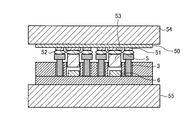
- 4I to 4J omit the holding unit 56, the driving unit 57, the heating / pressurizing unit 58, and the control unit 59 described in FIG. 4H.
- step S1 the setting process (step S1) for setting the pins 3 and the electronic components on the mounting jig 100 will be described.
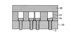
- the pin 3 is once set on a transfer jig 10 as shown in FIG. 4A.
- a through hole 11 having substantially the same diameter as the shaft portion 3b is formed in the transfer jig 10, and the pin 3 is placed on the transfer jig 10 and sucked by a vacuum pump or the like from the lower part of the transfer jig 10.
- the shaft portion 3 b is inserted into the through hole 11 and the pin 3 is set in the transfer jig 10.
- the pins 3 are transferred from the transfer jig 10 to the transfer jig 20.
- the transfer jig 20 is formed with an insertion hole 21 having substantially the same diameter as the connection portion 3a.
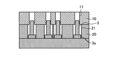
- the transfer jig 10 and the transfer jig 20 are connected as shown in FIG. 4C.
- the pin 3 is transferred from the transfer jig 10 to the transfer jig 20 by reversing the position so as not to shift.
- the pins 3 are transferred from the transfer jig 20 to the mounting jig 100.
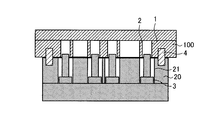
- the mounting jig 100 is placed from the side of the insertion hole 21 into which the pin 3 of the transfer jig 20 is inserted and positioned by the positioning pin 4, and as shown in FIG.
- the tool 20 and the mounting jig 100 are reversed, and the pin 3 is transferred from the transfer jig 20 to the pin insertion hole 1 of the mounting jig 100.
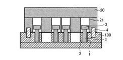
- the pin 3 By transferring the pin 3 by the transfer jig 20, as shown in FIG. 4F, the pin 3 is inserted into the pin insertion hole 1 of the mounting jig 100, and the empty electronic component insertion hole 2 is As shown in FIG. 4G, electronic components 5 such as capacitors are inserted by manual work or the like. It may be the electronic parts insertion hole 2 by inserting only the electronic component 5, when the height h 3 of the electronic component 5 is the electronic parts insertion hole 2 of the depth h 1 is less than, as shown in FIG.
- the spacer 6 is inserted below the component 5 so that the upper surface of the electronic component 5 is positioned above the upper surface of the mounting jig 100 and the positions of the upper surface of the pin 3 and the upper surface of the electronic component 5 are adjusted. .
- the height h 3 of the electronic component 5 mounted on the pin 3 at the same time as the substrate is generally not more than the height h 2 of the pin 3, the height h 3 of the electronic component 5 of the electronic parts insertion hole 2 depth h If it is smaller than 1 , the spacer 6 is used to adjust the height h 4 of the upper surface of the electronic component 5 to be larger than the depth h 1 of the electronic component insertion hole 2 and not more than the height h 2 of the pin 3.
- the height of the upper surface of the electronic component 5 can be increased by making the mounting jig 100 so that the depth of the electronic component insertion hole 2 is shallower than the depth of the pin insertion hole 1 without using the spacer 6. May be adjusted.
- the mounting surface of the electronic component 5 is defined, it is necessary to insert the electronic component 5 into the electronic component insertion hole 2 manually as described above. 3, the electronic component 5 may be inserted into the electronic component insertion hole 2 using a transfer jig, a transfer jig, or the like.
- the mounting method from FIG. 4A to FIG. 4G corresponds to step S1 in FIG.
- the mounting jig 100 on which the pin 3 and the electronic component 5 are set is placed on the stage of the mounting apparatus (step S2).
- the pin 3 and the electronic component 5 are connected to the substrate by a mounting device.
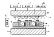
- the mounting apparatus includes a stage 55 on which a mounting jig 100 on which pins 3 and electronic components 5 are set, a holding unit 56 that holds the substrate 50 by suction, and a land 51 of the substrate 50.
- the solder 52 preliminarily applied to the land 51 of the substrate 50 and the drive unit 57 capable of moving the held substrate 50 up and down, and the solder 52 preliminarily applied to the connecting portion 3a of the pin 3 are heated.
- the head part 54 which has the heating and pressurizing part 58 which applies a pressure to the connection part 3a of the pin 3 which contacts 50, and the control part 59 which controls each part are provided.
- the mounting jig 100 is placed on the stage 55 of the mounting apparatus, and the solder 52 is applied to the lands 51 that connect the pins 3 and the lands 53 that connect the electronic components 5. 50 is held by the holding portion 56 and the substrate 50 is set on the head portion 54 side.
- the mounting method in FIG. 4H corresponds to step S2 in FIG.
- step S3 After the mounting jig 100 is set on the stage 55 of the mounting apparatus (step S2), the head portion 54 of the mounting apparatus that has attracted the substrate 50 is lowered, and the solder 52 and pins previously applied to the lands 51 of the substrate 50 3 is brought into contact with the connecting portion 3a (step S3).
- the head portion 54 that holds the substrate 50 is lowered by the drive portion 57 until the solder 52 and the connection portion 3a of the pin 3 come into contact with each other.
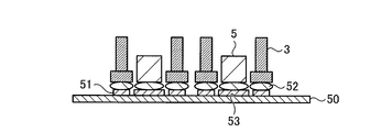
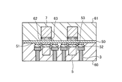
- the solder 52 is in contact with the connecting portion 3a of the pin 3 and heated while applying pressure by the heating / pressurizing portion 58, the solder 52 is melted. In the state before heating and pressurization, as shown in FIG.
- step S4 After the pins 3 and the electronic components 5 are collectively connected to the substrate 50 by heating and pressing (step S4), the substrate 50 and the mounting jig 100 are removed from the mounting apparatus, and the remaining flux is cleaned. As shown in 4K, the substrate 50 is separated from the mounting jig 100.
- the mounting method shown in FIGS. 4J to 4K corresponds to step S4 in FIG. Even if the electronic component insertion hole 2 and the pin insertion hole 1 of the mounting jig 100 have the same depth, the land 51 to which the pin 3 is connected is thicker than the land 53 to which the electronic component 5 is connected.
- the distance between the upper surface of the connection portion 3a of the pin 3 and the land 51 surface of the substrate 50 can be adjusted to be shorter than the distance between the upper surface of the electronic component 5 and the land 53 surface of the substrate 50. it can. Furthermore, by providing conductive protrusions (Au stud bumps, conductive paste, etc.) that are deformed by a load at the time of mounting on the lands 51 and 53 of the substrate 50, the load on the substrate 50 at the time of mounting can be reduced.
- conductive protrusions Au stud bumps, conductive paste, etc.
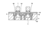
- the surface of the substrate 50 on which the pins 3 and the electronic components 5 are mounted is sealed with a sealing resin 60 and polished so that the end surfaces of the pins 3 are exposed on the surface of the sealing resin 60. (FIG. 4M).
- Another electronic component 7 is connected to the land 62 via the solder 63 on the back surface of the mounting surface such as the pin 3 of the substrate 50 (FIG. 4N), and the mounting surface of the electronic component 7 is also sealed with the sealing resin 61. It is stopped (FIG. 4O).
- the board 50 on which components are mounted on both sides is cut along a predetermined cut line indicated by a dotted line in FIG. 4P, and is separated into a mounting structure 70 (FIG. 4Q).
- the pins and the electronic components can be connected to the substrate all at once, and the mounting structure can be easily manufactured.
- the pins and electronic components are set on the mounting jig, it is possible to connect the electronic components without applying unnecessary pressure by adjusting the position of the top surfaces of the pins and the electronic components. Can be reduced.
- a spacer made of an elastic body can be used as the spacer of the mounting jig 100.
- the spacer 6A made of an elastic body it is preferable that the height h 5 of the upper surface of the electronic component 5 is higher than the height h 2 of the upper surface of the pin 3 as shown in FIG.
- the solder 52 comes into contact with the electronic component 5 first, but the pressure is mainly applied to the pin 3 because the spacer 6 ⁇ / b> A made of an elastic body is used. Accordingly, the pins 3 can be easily mounted in an upright state, and the electronic components 5 can be reliably connected while reducing the stress on the electronic components 5.
- the mounting method for aligning and setting the pins 3 and the electronic components 5 has been described by using the mounting jig 100, but the present invention is not limited thereto, and other methods may be used.
- the pin 3 and the electronic component 5 may be aligned and fixed using a member obtained by patterning a temporary adhesive sheet or a temporary adhesive.
- a method may be used in which a magnet is placed on a stage that is in contact with the back surface of the substrate 50 in accordance with the arrangement position of the pins 3 and the electronic components 5 and the pins and the electronic components are fixed using magnetic force.
- the imaging apparatus according to the second embodiment includes a mounting structure manufactured by the method of the first embodiment and an imaging element chip.
- FIG. 6 is a cross-sectional view schematically showing the imaging apparatus according to the second embodiment.
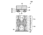
- the imaging apparatus 200 includes an imaging element chip 80, two mounting structures 71 ⁇ / b> A and 71 ⁇ / b> B, and a motherboard 90.
- the image sensor chip 80 is composed of a CMOS element or the like, and includes a light receiving unit 82 that photoelectrically converts an incident optical signal, a peripheral circuit unit 83 formed in the vicinity of the light receiving unit 82, and a TSV (Through-Silicon Via) or the like.
- the back surface electrode 85 formed in the back surface opposite to the surface in which the light-receiving part 82 was formed with the wiring 84 is provided.
- a glass lid 81 that protects the light receiving part 82 through a bonding layer is attached to the surface side.
- a wiring layer having a multilayer wiring structure is formed on the back surface of the imaging element chip 80.
- the image pickup device chip 80 is a CSP (Chip Size Package) in which the image pickup device in the wafer state is subjected to wiring, electrode formation, resin sealing, and dicing, and finally the size of the image pickup device becomes the size of the image pickup device chip. ) Is preferable.
- CSP Chip Size Package
- the mounting structures 71A and 71B have the same structure, the board 50, the connection pins 3a and the two pins 3 each having a shaft portion 3b having a smaller diameter than the connection portions 3a, and the height when mounting is high. And the following electronic component 5 and a sealing resin 60 that seals the mounting surface of the substrate 50 so that the end surface of the shaft portion 3b opposite to the connection portion 3a side is exposed.
- the mounting structures 71A and 71B are formed by the method described in the first embodiment. As shown in FIGS. 4A to 4M, the pins 3 mounted on the substrate 50 and the electronic component 5 are sealed with a sealing resin. After polishing so that the end surface of the shaft portion 3b of the pin 3 is exposed on the surface of the sealing resin 60, an electronic component is not mounted on the surface opposite to the mounting surface of the substrate 50 (FIG. 4N and FIG. 4O is omitted), and is cut into pieces by a predetermined cut line indicated by a dotted line in FIG. 4P.
- the two mounting structures 71A and 71B are mechanically and electrically connected to each other on the surface opposite to the mounting surface (the surface on which the electronic component 5 or the like is not mounted). Vias (not shown) are formed in the substrate 50, and the two mounting structures 71A and 71B are electrically connected by connection.
- the mother board 90 includes a connection electrode 91, is connected to the end surface of the shaft portion 3b exposed on the surface of the sealing resin 60 of the mounting structure 71B, and the periphery is sealed with the sealing resin 92. Further, bumps 86 made of solder are formed on the back electrode 85 of the image sensor chip 80, and are exposed to the surface of the sealing resin 60 of the mounting structure 71A via the bumps 86 as shown in FIG. It is connected to the end face of the shaft portion 3b. The periphery of the connection portion is sealed with a sealing resin 87.
- the imaging apparatus 200 uses the mounting structures 71A and 71B having the same structure, but if the end surfaces of the shaft portions of a plurality of pins can be used for connection to the imaging element chip 80 and the motherboard 90, Mounting structures containing different types of pins and electronic components may be used. Further, the number of pins 3 incorporated in the mounting structures 71A and 71B is not limited to this as long as it is two or more, and the number of electronic components 5 incorporated is also the same.
- FIG. 8 is a cross-sectional view schematically showing an imaging apparatus according to the first modification of the second embodiment.
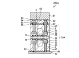
- the imaging device 200A includes an imaging element chip 80, a mounting structure 70A, and a motherboard 90.
- the two pins 3 and the electronic component 5 are mounted on the first surface f1 of the substrate 50, and the two pins 3 are also formed on the second surface f2 opposite to the first surface f1 of the substrate 50. And the electronic component 5 is mounted.
- the mounting structure 70A is formed by the method described in the first embodiment, and seals the pin 3 and the electronic component 5 mounted on the first surface f1 of the substrate 50 as shown in FIGS. 4A to 4M. After sealing with the stop resin 60 and polishing so that the end surface of the shaft portion 3b of the pin 3 is exposed to the surface of the sealing resin 60, the second surface f2 opposite to the first surface f1 of the substrate 50 is As shown in FIG. 9, the pin 3 and the electronic component 5 are mounted. Note that vias (not shown) are formed in the substrate 50, and the first surface f1 and the second surface f2 are electrically connected.
- FIG. 9 a mounting jig 100 in which pins 3 and electronic components 5 are set is placed on the stage 55 of the mounting apparatus, and the mounting structure before separation shown in FIG. Is sucked and held by the holding portion 56.
- Solder 52 is applied to the lands 51 that connect the pins 3 of the second surface f2 of the mounting structure before separation and the lands 53 that connect the electronic components 5, and the head unit 54 is lowered by the drive unit 57.
- the pin 3 and the land 51 and the electronic component 5 and the land 53 are respectively connected. Connection is performed in the same manner as in FIGS. 4H to 4J of the first embodiment, and in the same manner as in FIGS.
- the second surface f2 is sealed with the sealing resin 60, and the shaft portion 3b of the pin 3 is connected.
- the mounting structure 70 ⁇ / b> A is manufactured by being cut into pieces by a predetermined cut line.
- the same pin 3 and electronic component 5 are mounted on the first surface f1 and the second surface f2, but the end surfaces of the shaft portions of the plurality of pins Can be used for connection between the imaging element chip 80 and the mother board 90, different types of pins and electronic components may be incorporated in the first surface f1 and the second surface f2.
- the number of pins 3 mounted on the first surface f1 and the second surface f2 of the mounting structure 70A is not limited to this as long as it is two or more, and the number of electronic components 5 to be mounted is also limited. It is the same.
- the imaging apparatus may include a mounting structure manufactured by the method of Embodiment 1, an imaging element chip, and an aggregate cable.
- FIG. 10 is a cross-sectional view schematically showing an imaging apparatus according to the second modification of the second embodiment.
- the imaging device 250 includes an imaging element chip 80, two mounting structures 71 ⁇ / b> A and 71 ⁇ / b> B, and a collective cable 40.
- the aggregate cable 40 is a cable in which the outer sheath 43 at the ends of a plurality of cables 41 is peeled to expose the core wire 42 and the exposed core wire 42 is fixed by a fixing member 45 made of an insulating material such as resin.
- the core wire 42 is fixed at a predetermined interval by the fixing member 45, and the connection end face where the core wire 42 is exposed is polished.
- the exposed core wire 42 of the connection end face is connected to the shaft portion 3b by a bump 46 made of solder or the like formed on the shaft portion 3b exposed on the surface of the sealing resin 60 of the mounting structure 71B.
- the periphery of the connecting portion between the core wire 42 and the shaft portion 3 b is sealed with a sealing resin 47.
- the mounting structure for connecting the aggregate cable 40 may be the mounting structure 70A of the first modification.
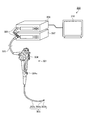
- FIG. 11 is a diagram schematically illustrating an overall configuration of an endoscope system including an imaging device.
- the endoscope system 300 includes an endoscope 301, a universal cord 305, a connector 306, a light source device 307, a processor (control device) 308, and a display device 310.
- the endoscope 301 captures an in-vivo image of the subject and outputs an imaging signal by inserting the insertion unit 303 into the body cavity of the subject.
- An imaging device 250 illustrated in FIG. 10 is disposed at the distal end portion 303 b and is connected to the light source device 307 and the processor 308 via the cable 41 inside the universal cord 305.
- the connector 306 is provided at the base end of the universal cord 305, is connected to the light source device 307 and the processor 308, and has a predetermined imaging signal (output signal) output from the imaging device 250 of the distal end portion 303b connected to the universal cord 305.
- the imaging signal is analog-digital converted (A / D converted) and output as an image signal.
- the light source device 307 is configured using, for example, a white LED.
- the pulsed white light that is turned on by the light source device 307 becomes illumination light that is emitted toward the subject from the distal end of the insertion portion 303 of the endoscope 301 via the connector 306 and the universal cord 305.
- the processor 308 performs predetermined image processing on the image signal output from the connector 306 and controls the entire endoscope system 300.
- the display device 310 displays the image signal processed by the processor 308.
- An operation unit 304 provided with various buttons and knobs for operating the endoscope function is connected to the proximal end side of the insertion unit 303 of the endoscope 301.
- the operation unit 304 is provided with a treatment instrument insertion port 304a for inserting a treatment instrument such as a biological forceps, an electric knife and an inspection probe into the body cavity of the subject.
- the insertion portion 303 includes a distal end portion 303b where the imaging device 250 is provided, a bending portion 303a that is connected to the proximal end side of the distal end portion 303b and can be bent in the vertical direction, and is connected to the proximal end side of the bending portion 303a.
- the bending portion 303a is bent in the vertical direction by operation of a bending operation knob provided in the operation portion 304, and can be bent in two directions, for example, up and down, as the bending wire inserted through the insertion portion 303 is pulled or loosened. It has become.
- a light guide that transmits illumination light from the light source device 307 is disposed, and an illumination window is disposed at an exit end of illumination light from the light guide.
- This illumination window is provided at the distal end portion 303b of the insertion portion 303, and the illumination light is irradiated toward the subject.
- the imaging device 250 is provided at the distal end of the insertion portion 303, and an image of an organ or the like obtained by inserting the insertion portion 303 into the body of the subject is displayed on the display device 310.
- the display device 310 By displaying on the display unit, it is possible to observe and diagnose the diagnosis target.
Landscapes
- Life Sciences & Earth Sciences (AREA)
- Health & Medical Sciences (AREA)
- Engineering & Computer Science (AREA)
- Surgery (AREA)
- Heart & Thoracic Surgery (AREA)
- Animal Behavior & Ethology (AREA)
- Nuclear Medicine, Radiotherapy & Molecular Imaging (AREA)
- Optics & Photonics (AREA)
- Pathology (AREA)
- Radiology & Medical Imaging (AREA)
- Physics & Mathematics (AREA)
- Biomedical Technology (AREA)
- Veterinary Medicine (AREA)
- Medical Informatics (AREA)
- Molecular Biology (AREA)
- Biophysics (AREA)
- General Health & Medical Sciences (AREA)
- Public Health (AREA)
- Mechanical Engineering (AREA)
- Manufacturing & Machinery (AREA)
- Endoscopes (AREA)
- Microelectronics & Electronic Packaging (AREA)
- Instruments For Viewing The Inside Of Hollow Bodies (AREA)
- Electric Connection Of Electric Components To Printed Circuits (AREA)
- Supply And Installment Of Electrical Components (AREA)
Abstract
Description
図1は、本発明の実施の形態1にかかる実装用治具を模式的に示す図である。図2は、図1に示す実装用治具のA-A線断面図である。図1に示すように、実装用治具100には、ピンを挿入するピン挿入穴1と、電子部品を挿入する電子部品挿入穴2と、を複数備える。
なお、電子部品5の実装面が規定される場合は、上記のように手作業で電子部品挿入穴2に挿入することが必要となるが、電子部品5の実装面が制限されない場合は、ピン3と同様に、振込治具や転写治具等を使用して電子部品5を電子部品挿入穴2に挿入してもよい。以上、図4Aから図4Gまでの実装方法が図3のステップS1に該当する。
また、ピン3と電子部品5を整列させてセットする実装方法として、実装用治具100を用いる方法で説明したが、これに限るものではなく、他の方法で整列させても良い。例えば、仮接着シートや仮接着剤をパターニングした部材を用いて、ピン3と電子部品5を整列させ固定しても良い。あるいは、ピン3と電子部品5の配列位置に応じて、基板50裏面に当接するステージに磁石を置き、磁力を用いてピンと電子部品を固定する方法を用いても良い。
実施の形態2にかかる撮像装置は、実施の形態1の方法により製造した実装構造体と、撮像素子チップとを備える。図6は、本実施の形態2にかかる撮像装置を模式的に示す断面図である。
2 電子部品挿入穴
3 ピン
3a 接続部
3b 軸部
4 位置決めピン
5、7 電子部品
6、6A スペーサ
10 振込治具
11 貫通穴
20 転写治具
21 挿入穴
40 集合ケーブル
41 ケーブル
42 芯線
43 外皮
45 固定部材
50 基板
51、53、62 ランド
52、63 半田
54 ヘッド部
55 ステージ
56 保持部
57 駆動部
58 加熱・加圧部
59 制御部
47、60、61、87、92 封止樹脂
70、70A、71A、71B 実装構造体
80 撮像素子チップ
81 ガラスリッド
82 受光部
83 周辺回路部
84 貫通配線
85 裏面電極
46、86 バンプ
90 マザーボード
91 接続電極
100 実装用治具
200、200A、250 撮像装置
300 内視鏡システム
301 内視鏡
303 挿入部
304 操作部
305 ユニバーサルコード
306 コネクタ
307 光源装置
308 プロセッサ
310 表示装置
Claims (14)
- 接続部および該接続部より細径の軸部からなる複数のピンと、実装時の高さが前記ピンの高さ以下の複数の電子部品とが基板の同一面に接続された実装構造体の製造方法であって、
前記複数のピンと前記複数の電子部品とを整列させてセットするセット工程と、
前記整列させた複数のピンおよび複数の電子部品を実装装置のステージに配置し、前記基板を吸着した実装装置のヘッド部を降下して、前記基板のランドに予め塗布された半田と前記ピンの接続部が接した状態で、加熱および加圧して前記ピンおよび前記電子部品とを前記基板表面に一括して接続する接続工程と、
を含むことを特徴とする実装構造体の製造方法。 - 前記セット工程は、
複数のピン挿入穴と複数の電子部品挿入穴とを備える実装用治具の前記ピン挿入穴に前記ピンの軸部をそれぞれ挿入するとともに、前記電子部品挿入穴に前記電子部品をそれぞれ挿入して、前記ピンと前記電子部品とを前記実装用治具にセットするものであり、
前記接続工程では、
前記ピンと前記電子部品とがセットされた前記実装用治具を実装装置のステージに配置することを特徴とする請求項1に記載の実装構造体の製造方法。 - 前記ピンと前記電子部品とを前記ピン挿入穴と前記電子部品挿入穴にそれぞれセットした際、前記ピンの接続部の上面と前記基板のランド面との距離の方が、前記電子部品の上面と前記基板のランド面との距離よりも短くなるように、前記電子部品挿入穴の深さ、および/または前記ランド面の厚みが調整されていることを特徴とする請求項2に記載の実装構造体の製造方法。
- 前記電子部品の上面と前記ピンの接続部の上面との位置を調整するスペーサを使用することで前記電子部品挿入穴の深さを調節することを特徴とする請求項3に記載の実装構造体の製造方法。
- 前記セット工程において、前記電子部品を、弾性体からなるスペーサを介して前記電子部品挿入穴にセットした際、前記電子部品の上面を前記ピンの接続部の上面より高くすることを特徴とする請求項2に記載の実装構造体の製造方法。
- 前記セット工程は、
振込治具にセットされた前記ピンを、前記接続部を下にして転写治具に移し替える転写工程と、
前記転写治具にセットされた前記ピンを前記実装用治具に移し替える第1のセット工程と、
前記電子部品を前記実装用治具にセットする第2のセット工程と、
を含むことを特徴とする請求項2~4のいずれか一つに記載の実装構造体の製造方法。 - 接続部および該接続部より細径の軸部からなる複数のピンと、実装時の高さが前記ピンの高さ以下の複数の電子部品とを基板の同一面に接続するための実装用治具であって、
前記ピンの軸部をそれぞれ挿入する複数のピン挿入穴と、
前記電子部品をそれぞれ挿入する複数の電子部品挿入穴と、
を有し、
前記ピンと前記電子部品とを前記ピン挿入穴と前記電子部品挿入穴にそれぞれセットした際、前記ピンの接続部の上面と前記電子部品の上面は実装用治具の上面より上部に位置するとともに、前記電子部品の上面は前記ピンの接続部の上面より低くなることを特徴とする実装用治具。 - 前記電子部品挿入穴に挿入する弾性体からなるスペーサを備え、
前記スペーサの挿入により、前記電子部品を前記電子部品挿入穴にセットした際、前記電子部品の上面が前記ピンの接続部の上面より高くなることを特徴とする請求項7に記載の実装用治具。 - 複数のピンと、前記ピンの高さ以下の複数の電子部品とが基板の同一面に接続された実装構造体の製造装置であって、
請求項7または8に記載の実装用治具と、
前記ピンと前記電子部品とがセットされた前記実装用治具を載置するステージと、
前記基板を吸着保持する保持部と、前記基板のランドに予め塗布された半田と前記ピンの接続部が接するように、保持した前記基板を上下動可能な駆動部と、前記基板のランドに予め塗布された半田を加熱し、前記基板と接する前記ピンの接続部に圧力を加える加熱・加圧部とを有するヘッド部と、
を備えることを特徴とする実装構造体の製造装置。 - 撮像素子チップと実装構造体とを備えた撮像装置において、
前記実装構造体は、
基板と、
前記基板の第1の面に実装され、第1の接続部および該第1の接続部より細径の第1の軸部からなる複数の第1のピンと、
前記基板の第1の面に実装され、実装時の高さが前記第1のピンの高さ以下の少なくとも1つの第1の電子部品と、
前記第1の軸部の前記第1の接続部側と反対側の端面が露出するように前記第1の面を封止する第1の封止樹脂と、
前記基板の第2の面に実装され、第2の接続部および該第2の接続部より細径の第2の軸部からなる複数の第2のピンと、
前記基板の第2の面に実装され、実装時の高さが前記第2のピンの高さ以下の少なくとも1つの第2の電子部品と、
前記第2の軸部の前記第2の接続部側と反対側の端面が露出するように前記第2の面を封止する第2の封止樹脂と、を有し、
前記撮像素子チップは、
入射した光信号を光電変換する受光部と、
貫通配線により前記受光部が形成された面と対向する面に形成された裏面電極と、を有し、
前記第1の封止樹脂上に露出した前記第1の軸部と前記裏面電極とを接続することにより、前記撮像素子チップと前記実装構造体とを接続することを特徴とする撮像装置。 - 接続電極を有するマザーボードを更に備え、
前記第2の封止樹脂上に露出した前記第2の軸部と前記接続電極とを接続することにより、前記マザーボードと前記実装構造体とを接続することを特徴とする請求項10に記載の撮像装置。 - 複数のケーブルを固定部材により固定した集合ケーブルを更に備え、
前記第2の封止樹脂上に露出した前記第2の軸部と、前記集合ケーブルの接続端面に露出した芯線とを接続することにより、前記集合ケーブルと前記実装構造体とを接続することを特徴とする請求項10に記載の撮像装置。 - 前記実装構造体は、請求項1~6のいずれか一つに記載の実装構造体の製造方法により製造されたことを特徴とする請求項10~12のいずれか一つに記載の撮像装置。
- 請求項10~13のいずれか一つに記載の撮像装置が先端に設けられた挿入部を備えたことを特徴とする内視鏡装置。
Priority Applications (4)
| Application Number | Priority Date | Filing Date | Title |
|---|---|---|---|
| DE112015001346.6T DE112015001346T8 (de) | 2014-03-20 | 2015-03-19 | Verfahren zur Herstellung einer Baueinheit, Zusammenbauschablone, Vorrichtung zur Herstellung der Baueinheit, Abbildungsvorrichtung und Endoskopvorrichtung |
| JP2016508810A JPWO2015141802A1 (ja) | 2014-03-20 | 2015-03-19 | 実装構造体の製造方法、実装用治具、実装構造体の製造装置、撮像装置および内視鏡装置 |
| CN201580014488.6A CN106104791B (zh) | 2014-03-20 | 2015-03-19 | 安装构造体的制造方法、安装用夹具、安装构造体的制造装置、摄像装置以及内窥镜装置 |
| US15/268,947 US10426324B2 (en) | 2014-03-20 | 2016-09-19 | Imaging apparatus including an image sensor chip mount assembly |
Applications Claiming Priority (4)
| Application Number | Priority Date | Filing Date | Title |
|---|---|---|---|
| JP2014059188 | 2014-03-20 | ||
| JP2014-059188 | 2014-03-20 | ||
| JP2015-004487 | 2015-01-13 | ||
| JP2015004487 | 2015-01-13 |
Related Child Applications (1)
| Application Number | Title | Priority Date | Filing Date |
|---|---|---|---|
| US15/268,947 Continuation US10426324B2 (en) | 2014-03-20 | 2016-09-19 | Imaging apparatus including an image sensor chip mount assembly |
Publications (1)
| Publication Number | Publication Date |
|---|---|
| WO2015141802A1 true WO2015141802A1 (ja) | 2015-09-24 |
Family
ID=54144764
Family Applications (1)
| Application Number | Title | Priority Date | Filing Date |
|---|---|---|---|
| PCT/JP2015/058345 Ceased WO2015141802A1 (ja) | 2014-03-20 | 2015-03-19 | 実装構造体の製造方法、実装用治具、実装構造体の製造装置、撮像装置および内視鏡装置 |
Country Status (5)
| Country | Link |
|---|---|
| US (1) | US10426324B2 (ja) |
| JP (1) | JPWO2015141802A1 (ja) |
| CN (1) | CN106104791B (ja) |
| DE (1) | DE112015001346T8 (ja) |
| WO (1) | WO2015141802A1 (ja) |
Cited By (1)
| Publication number | Priority date | Publication date | Assignee | Title |
|---|---|---|---|---|
| JP2020028936A (ja) * | 2018-08-22 | 2020-02-27 | ガウス株式会社 | 微小部品表面処理システム及び微小部品表面処理方法 |
Families Citing this family (4)
| Publication number | Priority date | Publication date | Assignee | Title |
|---|---|---|---|---|
| US11395406B2 (en) | 2015-06-11 | 2022-07-19 | Scoutcam Ltd. | Camera head |
| IL239386B (en) * | 2015-06-11 | 2018-07-31 | Medigus Ltd | Video camera head |
| WO2020110199A1 (ja) | 2018-11-27 | 2020-06-04 | オリンパス株式会社 | ケーブル接続構造 |
| CN118829186A (zh) * | 2023-04-17 | 2024-10-22 | 台达电子工业股份有限公司 | 插件深度的学习方法 |
Citations (7)
| Publication number | Priority date | Publication date | Assignee | Title |
|---|---|---|---|---|
| JPH0435474A (ja) * | 1990-05-30 | 1992-02-06 | Olympus Optical Co Ltd | 固体撮像装置 |
| JPH10270144A (ja) * | 1997-03-26 | 1998-10-09 | Ibiden Co Ltd | 端子付き基板製造用治具 |
| JP2006025852A (ja) * | 2004-07-12 | 2006-02-02 | Texas Instr Japan Ltd | 内視鏡用撮像モジュール |
| JP2006216631A (ja) * | 2005-02-02 | 2006-08-17 | Ngk Spark Plug Co Ltd | 配線基板およびその製造方法 |
| JP2009239223A (ja) * | 2008-03-28 | 2009-10-15 | Ngk Spark Plug Co Ltd | 多層配線基板 |
| WO2011030608A1 (ja) * | 2009-09-11 | 2011-03-17 | オリンパスメディカルシステムズ株式会社 | 撮像装置及び撮像装置の製造方法 |
| JP2011188375A (ja) * | 2010-03-10 | 2011-09-22 | Olympus Corp | 撮像装置 |
Family Cites Families (13)
| Publication number | Priority date | Publication date | Assignee | Title |
|---|---|---|---|---|
| US6691400B1 (en) * | 1995-12-15 | 2004-02-17 | Matsushita Electric Industrial Co., Ltd. | High speed electronic parts mounting apparatus having mounting heads which alternately mount components on a printed circuit board |
| JP3358464B2 (ja) * | 1996-10-11 | 2002-12-16 | 松下電器産業株式会社 | 電子部品実装方法 |
| JP2000307238A (ja) | 1999-04-19 | 2000-11-02 | Sumitomo Metal Electronics Devices Inc | ピン振込み治具およびプリント基板へのピンの取付方法 |
| JP2001024312A (ja) | 1999-07-13 | 2001-01-26 | Taiyo Yuden Co Ltd | 電子装置の製造方法及び電子装置並びに樹脂充填方法 |
| DE102004056946A1 (de) * | 2004-11-23 | 2006-05-24 | Karl Storz Gmbh & Co. Kg | Bildaufnehmermodul sowie Verfahren zum Zusammenbauen eines Bildaufnehmermoduls |
| JP2007220837A (ja) * | 2006-02-16 | 2007-08-30 | Juki Corp | 電子部品実装方法及び装置 |
| JP2008168042A (ja) * | 2007-01-15 | 2008-07-24 | Olympus Corp | 積層実装構造体 |
| JP2008177298A (ja) * | 2007-01-17 | 2008-07-31 | Olympus Corp | 積層実装構造体 |
| JP2012084742A (ja) * | 2010-10-13 | 2012-04-26 | Hitachi Cable Ltd | リフロ用治具及びリフロ加熱方法 |
| JP5926890B2 (ja) * | 2011-03-04 | 2016-05-25 | オリンパス株式会社 | 配線板、配線板の製造方法、および撮像装置 |
| JP5757852B2 (ja) * | 2011-12-05 | 2015-08-05 | オリンパス株式会社 | 撮像モジュールおよび撮像ユニット |
| JP6205184B2 (ja) * | 2013-06-17 | 2017-09-27 | オリンパス株式会社 | 電子部品実装構造体 |
| US20150351218A1 (en) * | 2014-05-27 | 2015-12-03 | Fujikura Ltd. | Component built-in board and method of manufacturing the same, and mounting body |
-
2015
- 2015-03-19 DE DE112015001346.6T patent/DE112015001346T8/de not_active Expired - Fee Related
- 2015-03-19 WO PCT/JP2015/058345 patent/WO2015141802A1/ja not_active Ceased
- 2015-03-19 CN CN201580014488.6A patent/CN106104791B/zh not_active Expired - Fee Related
- 2015-03-19 JP JP2016508810A patent/JPWO2015141802A1/ja not_active Ceased
-
2016
- 2016-09-19 US US15/268,947 patent/US10426324B2/en active Active
Patent Citations (7)
| Publication number | Priority date | Publication date | Assignee | Title |
|---|---|---|---|---|
| JPH0435474A (ja) * | 1990-05-30 | 1992-02-06 | Olympus Optical Co Ltd | 固体撮像装置 |
| JPH10270144A (ja) * | 1997-03-26 | 1998-10-09 | Ibiden Co Ltd | 端子付き基板製造用治具 |
| JP2006025852A (ja) * | 2004-07-12 | 2006-02-02 | Texas Instr Japan Ltd | 内視鏡用撮像モジュール |
| JP2006216631A (ja) * | 2005-02-02 | 2006-08-17 | Ngk Spark Plug Co Ltd | 配線基板およびその製造方法 |
| JP2009239223A (ja) * | 2008-03-28 | 2009-10-15 | Ngk Spark Plug Co Ltd | 多層配線基板 |
| WO2011030608A1 (ja) * | 2009-09-11 | 2011-03-17 | オリンパスメディカルシステムズ株式会社 | 撮像装置及び撮像装置の製造方法 |
| JP2011188375A (ja) * | 2010-03-10 | 2011-09-22 | Olympus Corp | 撮像装置 |
Cited By (1)
| Publication number | Priority date | Publication date | Assignee | Title |
|---|---|---|---|---|
| JP2020028936A (ja) * | 2018-08-22 | 2020-02-27 | ガウス株式会社 | 微小部品表面処理システム及び微小部品表面処理方法 |
Also Published As
| Publication number | Publication date |
|---|---|
| US20170000321A1 (en) | 2017-01-05 |
| CN106104791B (zh) | 2019-05-14 |
| DE112015001346T8 (de) | 2017-02-09 |
| US10426324B2 (en) | 2019-10-01 |
| DE112015001346T5 (de) | 2016-12-01 |
| JPWO2015141802A1 (ja) | 2017-04-13 |
| CN106104791A (zh) | 2016-11-09 |
Similar Documents
| Publication | Publication Date | Title |
|---|---|---|
| US10653306B2 (en) | Electronic circuit unit, imaging unit, and endoscope | |
| US10426324B2 (en) | Imaging apparatus including an image sensor chip mount assembly | |
| CN105578946B (zh) | 摄像单元和内窥镜装置 | |
| US10898060B2 (en) | Cable connection structure, endoscope system, and method of manufacturing cable connection structure | |
| JP6358806B2 (ja) | ケーブル実装構造体、ケーブル接続構造体、内視鏡装置 | |
| US20170255001A1 (en) | Imaging unit, endoscope, and method of manufacturing imaging unit | |
| US10617285B2 (en) | Imaging module with multi-layer substrate and endoscope apparatus | |
| JP6570657B2 (ja) | 撮像装置、内視鏡および撮像装置の製造方法 | |
| WO2016111075A1 (ja) | 撮像ユニット、撮像モジュールおよび内視鏡システム | |
| JP6043032B2 (ja) | 内視鏡 | |
| WO2017195605A1 (ja) | 電子回路ユニット、撮像ユニット、撮像モジュールおよび内視鏡 | |
| US10734355B2 (en) | Electronic circuit board, laminated board, and method of manufacturing electronic circuit board | |
| JP6099541B2 (ja) | 内視鏡及び内視鏡の製造方法 | |
| CN106455933B (zh) | 缆线连接构造和内窥镜装置 | |
| JP6726531B2 (ja) | 内視鏡 | |
| WO2019193911A1 (ja) | 撮像ユニット、および内視鏡 | |
| WO2020089960A1 (ja) | 撮像装置、内視鏡、および、撮像装置の製造方法 | |
| WO2018003510A1 (ja) | 撮像ユニット、および内視鏡 | |
| JP2015080633A (ja) | 電気ユニット及び電気ユニットを用いた内視鏡装置 |
Legal Events
| Date | Code | Title | Description |
|---|---|---|---|
| 121 | Ep: the epo has been informed by wipo that ep was designated in this application |
Ref document number: 15765486 Country of ref document: EP Kind code of ref document: A1 |
|
| ENP | Entry into the national phase |
Ref document number: 2016508810 Country of ref document: JP Kind code of ref document: A |
|
| WWE | Wipo information: entry into national phase |
Ref document number: 112015001346 Country of ref document: DE |
|
| 122 | Ep: pct application non-entry in european phase |
Ref document number: 15765486 Country of ref document: EP Kind code of ref document: A1 |