WO2015137448A1 - El素子、el素子用基板、照明装置、ディスプレイ装置、及び液晶ディスプレイ装置 - Google Patents
El素子、el素子用基板、照明装置、ディスプレイ装置、及び液晶ディスプレイ装置 Download PDFInfo
- Publication number
- WO2015137448A1 WO2015137448A1 PCT/JP2015/057300 JP2015057300W WO2015137448A1 WO 2015137448 A1 WO2015137448 A1 WO 2015137448A1 JP 2015057300 W JP2015057300 W JP 2015057300W WO 2015137448 A1 WO2015137448 A1 WO 2015137448A1
- Authority
- WO
- WIPO (PCT)
- Prior art keywords
- light
- layer
- light scattering
- refractive index
- substrate
- Prior art date
- Legal status (The legal status is an assumption and is not a legal conclusion. Google has not performed a legal analysis and makes no representation as to the accuracy of the status listed.)
- Ceased
Links
Images





Classifications
-
- G—PHYSICS
- G02—OPTICS
- G02F—OPTICAL DEVICES OR ARRANGEMENTS FOR THE CONTROL OF LIGHT BY MODIFICATION OF THE OPTICAL PROPERTIES OF THE MEDIA OF THE ELEMENTS INVOLVED THEREIN; NON-LINEAR OPTICS; FREQUENCY-CHANGING OF LIGHT; OPTICAL LOGIC ELEMENTS; OPTICAL ANALOGUE/DIGITAL CONVERTERS
- G02F1/00—Devices or arrangements for the control of the intensity, colour, phase, polarisation or direction of light arriving from an independent light source, e.g. switching, gating or modulating; Non-linear optics
- G02F1/01—Devices or arrangements for the control of the intensity, colour, phase, polarisation or direction of light arriving from an independent light source, e.g. switching, gating or modulating; Non-linear optics for the control of the intensity, phase, polarisation or colour
- G02F1/13—Devices or arrangements for the control of the intensity, colour, phase, polarisation or direction of light arriving from an independent light source, e.g. switching, gating or modulating; Non-linear optics for the control of the intensity, phase, polarisation or colour based on liquid crystals, e.g. single liquid crystal display cells
- G02F1/133—Constructional arrangements; Operation of liquid crystal cells; Circuit arrangements
- G02F1/1333—Constructional arrangements; Manufacturing methods
- G02F1/1335—Structural association of cells with optical devices, e.g. polarisers or reflectors
- G02F1/1336—Illuminating devices
- G02F1/133602—Direct backlight
- G02F1/133606—Direct backlight including a specially adapted diffusing, scattering or light controlling members
-
- G—PHYSICS
- G02—OPTICS
- G02B—OPTICAL ELEMENTS, SYSTEMS OR APPARATUS
- G02B5/00—Optical elements other than lenses
- G02B5/02—Diffusing elements; Afocal elements
- G02B5/0205—Diffusing elements; Afocal elements characterised by the diffusing properties
- G02B5/0236—Diffusing elements; Afocal elements characterised by the diffusing properties the diffusion taking place within the volume of the element
- G02B5/0242—Diffusing elements; Afocal elements characterised by the diffusing properties the diffusion taking place within the volume of the element by means of dispersed particles
-
- H—ELECTRICITY
- H10—SEMICONDUCTOR DEVICES; ELECTRIC SOLID-STATE DEVICES NOT OTHERWISE PROVIDED FOR
- H10K—ORGANIC ELECTRIC SOLID-STATE DEVICES
- H10K50/00—Organic light-emitting devices
- H10K50/80—Constructional details
- H10K50/805—Electrodes
- H10K50/82—Cathodes
- H10K50/828—Transparent cathodes, e.g. comprising thin metal layers
-
- H—ELECTRICITY
- H10—SEMICONDUCTOR DEVICES; ELECTRIC SOLID-STATE DEVICES NOT OTHERWISE PROVIDED FOR
- H10K—ORGANIC ELECTRIC SOLID-STATE DEVICES
- H10K50/00—Organic light-emitting devices
- H10K50/80—Constructional details
- H10K50/85—Arrangements for extracting light from the devices
- H10K50/854—Arrangements for extracting light from the devices comprising scattering means
-
- H—ELECTRICITY
- H10—SEMICONDUCTOR DEVICES; ELECTRIC SOLID-STATE DEVICES NOT OTHERWISE PROVIDED FOR
- H10K—ORGANIC ELECTRIC SOLID-STATE DEVICES
- H10K50/00—Organic light-emitting devices
- H10K50/80—Constructional details
- H10K50/85—Arrangements for extracting light from the devices
- H10K50/856—Arrangements for extracting light from the devices comprising reflective means
-
- H—ELECTRICITY
- H10—SEMICONDUCTOR DEVICES; ELECTRIC SOLID-STATE DEVICES NOT OTHERWISE PROVIDED FOR
- H10K—ORGANIC ELECTRIC SOLID-STATE DEVICES
- H10K59/00—Integrated devices, or assemblies of multiple devices, comprising at least one organic light-emitting element covered by group H10K50/00
- H10K59/80—Constructional details
- H10K59/875—Arrangements for extracting light from the devices
- H10K59/877—Arrangements for extracting light from the devices comprising scattering means
-
- H—ELECTRICITY
- H10—SEMICONDUCTOR DEVICES; ELECTRIC SOLID-STATE DEVICES NOT OTHERWISE PROVIDED FOR
- H10K—ORGANIC ELECTRIC SOLID-STATE DEVICES
- H10K77/00—Constructional details of devices covered by this subclass and not covered by groups H10K10/80, H10K30/80, H10K50/80 or H10K59/80
- H10K77/10—Substrates, e.g. flexible substrates
-
- G—PHYSICS
- G02—OPTICS
- G02F—OPTICAL DEVICES OR ARRANGEMENTS FOR THE CONTROL OF LIGHT BY MODIFICATION OF THE OPTICAL PROPERTIES OF THE MEDIA OF THE ELEMENTS INVOLVED THEREIN; NON-LINEAR OPTICS; FREQUENCY-CHANGING OF LIGHT; OPTICAL LOGIC ELEMENTS; OPTICAL ANALOGUE/DIGITAL CONVERTERS
- G02F1/00—Devices or arrangements for the control of the intensity, colour, phase, polarisation or direction of light arriving from an independent light source, e.g. switching, gating or modulating; Non-linear optics
- G02F1/01—Devices or arrangements for the control of the intensity, colour, phase, polarisation or direction of light arriving from an independent light source, e.g. switching, gating or modulating; Non-linear optics for the control of the intensity, phase, polarisation or colour
- G02F1/13—Devices or arrangements for the control of the intensity, colour, phase, polarisation or direction of light arriving from an independent light source, e.g. switching, gating or modulating; Non-linear optics for the control of the intensity, phase, polarisation or colour based on liquid crystals, e.g. single liquid crystal display cells
- G02F1/133—Constructional arrangements; Operation of liquid crystal cells; Circuit arrangements
- G02F1/1333—Constructional arrangements; Manufacturing methods
- G02F1/1335—Structural association of cells with optical devices, e.g. polarisers or reflectors
- G02F1/1336—Illuminating devices
- G02F1/133602—Direct backlight
- G02F1/133606—Direct backlight including a specially adapted diffusing, scattering or light controlling members
- G02F1/133607—Direct backlight including a specially adapted diffusing, scattering or light controlling members the light controlling member including light directing or refracting elements, e.g. prisms or lenses
-
- G—PHYSICS
- G02—OPTICS
- G02F—OPTICAL DEVICES OR ARRANGEMENTS FOR THE CONTROL OF LIGHT BY MODIFICATION OF THE OPTICAL PROPERTIES OF THE MEDIA OF THE ELEMENTS INVOLVED THEREIN; NON-LINEAR OPTICS; FREQUENCY-CHANGING OF LIGHT; OPTICAL LOGIC ELEMENTS; OPTICAL ANALOGUE/DIGITAL CONVERTERS
- G02F2201/00—Constructional arrangements not provided for in groups G02F1/00 - G02F7/00
- G02F2201/44—Arrangements combining different electro-active layers, e.g. electrochromic, liquid crystal or electroluminescent layers
-
- H—ELECTRICITY
- H10—SEMICONDUCTOR DEVICES; ELECTRIC SOLID-STATE DEVICES NOT OTHERWISE PROVIDED FOR
- H10K—ORGANIC ELECTRIC SOLID-STATE DEVICES
- H10K59/00—Integrated devices, or assemblies of multiple devices, comprising at least one organic light-emitting element covered by group H10K50/00
- H10K59/80—Constructional details
- H10K59/875—Arrangements for extracting light from the devices
- H10K59/878—Arrangements for extracting light from the devices comprising reflective means
-
- Y—GENERAL TAGGING OF NEW TECHNOLOGICAL DEVELOPMENTS; GENERAL TAGGING OF CROSS-SECTIONAL TECHNOLOGIES SPANNING OVER SEVERAL SECTIONS OF THE IPC; TECHNICAL SUBJECTS COVERED BY FORMER USPC CROSS-REFERENCE ART COLLECTIONS [XRACs] AND DIGESTS
- Y02—TECHNOLOGIES OR APPLICATIONS FOR MITIGATION OR ADAPTATION AGAINST CLIMATE CHANGE
- Y02E—REDUCTION OF GREENHOUSE GAS [GHG] EMISSIONS, RELATED TO ENERGY GENERATION, TRANSMISSION OR DISTRIBUTION
- Y02E10/00—Energy generation through renewable energy sources
- Y02E10/50—Photovoltaic [PV] energy
- Y02E10/549—Organic PV cells
Definitions
- the present invention relates to an EL element (electroluminescence element), an EL element substrate, a lighting device, a display device, and a liquid crystal display device.
- EL elements as display units and light sources (display light sources) or illumination light sources in illumination devices, display devices, and liquid crystal display devices are known.
- an EL element for example, a light emitting structure in which a light emitting layer containing a fluorescent organic compound is sandwiched between an anode and a cathode is known.
- an organic EL element having a structure in which this light emitting structure is provided on one side of a light transmitting substrate is used.
- an exciton is generated by applying a direct voltage between the anode and the cathode, injecting electrons and holes into the light emitting layer and recombining them, and the exciton is deactivated.
- the organic EL element emits light by utilizing the emission of light.
- the electrode which comprises a light emitting structure the electrode of the light extraction side is comprised with a transparent electrode at least.
- an anode provided on a translucent substrate is formed of a transparent electrode, and light emitted from the light emitting layer is emitted outside through the transparent electrode and the translucent substrate.
- Patent Document 1 proposes forming a microlens array in which a plurality of microlens elements are arranged in a plane on one surface of a translucent substrate.
- Patent Document 2 describes a configuration in which transparent particles having a refractive index difference are dispersed in a transparent resin matrix as a layer having a light scattering function on the light extraction surface side of a high refractive index layer.
- the prior art as described above has the following problems.
- the microlens element is provided on the surface of the translucent substrate as in the technique described in Patent Document 1, depending on the incident angle to the microlens element, there is a light component reflected to the light emitting layer side.
- a light component is liable to cause a light amount loss by returning to the inside of the EL element. Therefore, in the technique described in Patent Document 1, although the light extraction efficiency can be improved as compared with the case where the microlens element is not provided, it has been strongly demanded to further improve the light extraction efficiency.
- the refractive index of the transparent electrode used in the light emitting structure is higher than that of a general transparent resin or glass.
- the transparent resin matrix of the layer having a light scattering function adjacent to the transparent electrode (hereinafter referred to as a light scattering layer) is used to suppress total reflection at the interface between the transparent resin matrix and the transparent electrode.
- a high refractive index material close to the refractive index.
- even a resin material that can disperse transparent particles has a high refractive index, which is not as high as that of a transparent electrode.
- the transparent particles used for scattering tend to agglomerate inside the transparent resin matrix, and if the aggregation of the transparent particles adversely affects the light scattering performance and transmittance, the blending amount is limited. For this reason, a technique for further improving the light extraction efficiency using a light scattering layer has been strongly desired.
- the present invention has been made in view of the above problems, and an object thereof is to provide an EL element and an EL element substrate that can improve light extraction efficiency. It is another object of the present invention to provide an illumination device, a display device, and a liquid crystal display device that can reduce power consumption (improve power saving performance) by including such an EL element. .
- the EL device includes an EL light emitting unit in which a transparent electrode, a light emitting layer, and a counter electrode are laminated in this order, and an optical element having an uneven shape and emitting light generated in the light emitting layer to the outside.
- a light-transmitting substrate having a sheet disposed on the surface and light scattering particles are formed, and an uneven shape is formed by an aggregate in which the light scattering particles are aggregated, and facing the transparent electrode of the EL light emitting unit.
- the light scattering particles in a dense state are aligned along a smooth surface as compared to the uneven shape of the first surface and have a second surface facing the light-transmitting substrate.
- a light scattering layer disposed between the EL light emitting unit and the translucent substrate.
- the light scattering layer is formed by passing the transparent electrode through a light-transmitting smoothing layer that forms a smooth joint surface that covers the uneven shape on the first surface. And may be joined.
- the EL element according to the first aspect of the present invention further includes a light-transmitting sheet-like base material bonded to the surface facing the light scattering layer in the light-transmitting substrate via a bonding layer.
- the light scattering particles provided on the second surface may be aligned along a surface of the substrate opposite to the surface on which the bonding layer is provided.
- the light scattering particles provided on the second surface are aligned along a surface of the translucent substrate opposite to the surface on which the optical sheet is disposed. May be.
- the light scattering particles of the light scattering layer may have a particle density on the second surface higher than that on the first surface.
- the light scattering particles of the light scattering layer may have an average particle size on the second surface smaller than an average particle size on the first surface.
- the lighting device includes the EL element according to the first aspect described above as a light emitting unit.
- the display device includes the EL element according to the first aspect described above, and the EL light emitting unit of the EL element has a plurality of pixels that can be driven independently.
- a liquid crystal display device includes an image display element using liquid crystal, and the EL element according to the first aspect, which is disposed on the back surface of the image display element.
- a liquid crystal display device includes an image display element using liquid crystal and the illumination device according to the second aspect described above, disposed on the back surface of the image display element.
- a light emitting structure having at least one electrode pair made of a transparent electrode and a light emitting layer sandwiched between the electrode pairs is disposed to form an EL element.
- the EL element substrate according to the sixth aspect of the present invention includes a light-transmitting substrate, a light-transmitting refractive index adjusting particle, and a light-transmitting binder.
- the weight ratio W H of the refractive index adjusting particles to the binder, the weight ratio W A of the scattering particles to the binder is, satisfies the following formula (1). 2 ⁇ W H / W A ⁇ 9 (1)
- the refractive index of the scattering particles is n A and the refractive index of the base material portion is n BH
- the following formula (2) may be satisfied. . 0.05 ⁇
- the refractive index adjusting particles are polydisperse particles having a particle size distributed in a range of 1 nm to 300 nm, and the scattering particles are the scattering particles.
- the average particle diameter is R A and the film thickness of the light scattering layer is H
- monodisperse particles satisfying the following formula (3) may be used. 1.5 ⁇ H / R A ⁇ 20 (3)
- An EL device includes a light emitting structure including the EL device substrate according to the sixth aspect described above, an electrode pair at least one of which is made of a transparent electrode, and a light emitting layer sandwiched between the electrode pairs.
- the translucent substrate of the EL element substrate has a refractive index lower than the refractive index of the transparent electrode, and the transparent electrode of the light emitting structure includes the translucent substrate and the transparent substrate It arrange
- the light emitting structure may form a plurality of pixels that can be driven independently.
- the illumination device includes the EL element according to the seventh aspect described above as an illumination light source.
- the display device includes the EL element according to the seventh aspect described above as a display unit.
- a liquid crystal display device includes an image display element using liquid crystal, and the EL element according to the seventh aspect, which is disposed as an illumination light source on the back surface of the image display element.
- a liquid crystal display device includes an image display element using liquid crystal, and the illumination device according to the eighth aspect described above, which is disposed on the back surface of the image display element.
- the light scattering layer in which the arrangement of the light scattering particles is changed between the first surface facing the transparent electrode and the second surface facing the translucent substrate is provided.
- the light extraction efficiency can be improved.
- the illuminating device, display apparatus, and liquid crystal display device which concern on the said aspect of this invention, since the EL element which concerns on the said aspect of this invention is provided, there exists an effect that power saving performance can be improved.
- the light scattering layer is a base material adjusted to have a higher refractive index than the translucent substrate in which the refractive index adjusting particles and the binder are blended. part and and a scattering particles, the weight ratio W H refractive index adjusting particles to binder, and below 9 times 2 times the weight ratio W a of the scattering particles. For this reason, the light extraction efficiency of the light incident on the light emitting structure of the EL element can be improved.
- the illuminating device, display apparatus, and liquid crystal display device which concern on the said aspect of this invention, there exists an effect that power consumption can be reduced by providing the EL element which concerns on the said aspect of this invention.
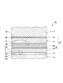
- FIG. 1 is a schematic cross-sectional view showing a configuration of a liquid crystal display device and an EL element according to the first embodiment of the present invention.
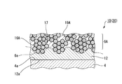
- FIG. 2 is a schematic partial enlarged view of a portion A in FIG. 3A is a schematic partial enlarged view of a portion C in FIG.
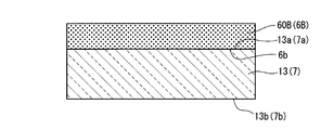
- FIG. 3B is a schematic partial enlarged view of a portion D in FIG.
- the scale of each member is appropriately changed to make each member a recognizable size.
- the liquid crystal display device 50 includes a liquid crystal panel 11 (image display element) and the EL element 10 according to the first embodiment.
- EL represents electroluminescence.
- the liquid crystal panel 11 is an image display element using liquid crystal, and although various detailed configurations are omitted, various known configurations can be adopted.
- a configuration suitable for the liquid crystal panel 11 for example, the light transmittance in pixels arranged in a rectangular shape in plan view is controlled, and the polarization state of the liquid crystal layer sandwiched between polarizing plates is controlled independently for each pixel. It is possible to adopt a configuration in which image display is performed by changing the above. In this case, the polarization state of the liquid crystal layer is controlled by applying an electric field corresponding to the image signal by an electrode (not shown) arranged for each pixel.
- the EL element 10 is a light emitting unit (light emitting device) that is disposed on the back surface of the liquid crystal panel 11 and illuminates the liquid crystal panel 11 from the back surface, and constitutes an illumination device in the liquid crystal display device 50. Yes. For this reason, the EL element 10 only needs to irradiate the liquid crystal panel 11 with uniform illumination light.
- the EL element 10 has a plurality of light emitting pixels that can emit light independently.
- FIG. 1 shows a configuration of one light emitting pixel. For this reason, in the EL element 10, a plurality of configurations as illustrated are formed adjacent to each other in the illustrated left-right direction and illustrated depth direction.
- the schematic configuration of the EL element 10 includes a configuration in which the counter substrate 1, the light emitting structure 5 (EL light emitting unit), the light scattering layer 6, the translucent substrate 7, and the light directing film 9 are laminated in this order.
- the light emitting structure 5 is a device portion that generates illumination light to be emitted to the liquid crystal panel 11 by EL light emission.
- the light B0 generated in the light emitting structure 5 passes through the light scattering layer 6, the translucent substrate 7, and the light directing film 9, and is emitted to the outside as the light B1, and the liquid crystal panel 11 Is irradiated.
- “translucency” means translucency regarding the wavelength light of the light B0 generated in the light emitting structure 5 unless otherwise specified.
- the counter substrate 1 and the translucent substrate 7 are plate-like or sheet-like members arranged to face each other in order to sandwich the light emitting structure 5 and the light scattering layer 6 therebetween.
- the counter substrate 1 forms one outer surface perpendicular to the thickness direction of the EL element 10. Since the counter substrate 1 does not particularly need translucency, an appropriate material on which the light emitting structure 5 can be laminated, for example, synthetic resin, glass, metal, or the like can be used. In the first embodiment, as an example, the same material as that of the translucent substrate 7 described later is employed.
- the light transmittance of the translucent substrate 7 is preferably 50% or more and more preferably 80% or more as the total light transmittance.
- various glass materials can be used.
- synthetic resin materials such as PMMA (polymethyl methacrylate resin), polycarbonate, polystyrene, PEN (polyethylene naphthalate resin), and PET (polyethylene terephthalate resin) can be used.
- a synthetic resin material is used, a particularly preferable material is a cycloolefin-based polymer. This polymer is an excellent material in all of the material properties such as processability, heat resistance, water resistance, and optical translucency.
- the transparent electrode 4, the light emitting layer 3, and the counter electrode 2 are stacked in this order, and the counter electrode 2 is disposed on the counter substrate 1 with the counter electrode 2 facing the counter substrate 1.
- the light emitting layer 3 emits light by applying a voltage to the transparent electrode 4 and the counter electrode 2.
- various conventionally known structures can be employed as the structure of the light emitting structure 5.
- the transparent electrode 4 is one electrode (first electrode) for applying a voltage to the light emitting layer 3, and is made of a material that can transmit the light B0.
- Examples of such a light-transmitting electrode material include ITO (indium tin oxide).
- the counter electrode 2 is the other electrode (second electrode) for applying a voltage to the light emitting layer 3.
- the material of the counter electrode 2 can be the same as that of the transparent electrode 4.
- the material of the counter electrode 2 is an appropriate metal material having good conductivity, such as aluminum, silver, copper, etc. Can also be adopted.
- the counter electrode 2 in order to emit as much light B0 as possible from the light directing film 9, the counter electrode 2 is preferably made of a material having a good light reflection function.
- the light reflectance of the counter electrode 2 is preferably 50% or more and 100% or less.
- the counter electrode 2 When the counter electrode 2 is made of a material having low light reflectance or a transparent material, it is preferable to provide a light reflecting layer between the counter electrode 2 and the counter substrate 1.
- the light reflecting layer may be provided between the counter electrode 2 and the counter substrate 1, or may be provided on the counter substrate 1 or the counter electrode 2, or may be provided inside the counter substrate 1. is there.
- the counter substrate 1 itself can be made of a light-reflective material so that the counter substrate 1 can also serve as a light reflection layer.
- the polarities of the transparent electrode 4 and the counter electrode 2 are not particularly limited, but in the first embodiment, as an example, the transparent electrode 4 is used as an anode and the counter electrode 2 is used as a cathode.
- the light emitting layer 3 can be a white light emitting layer, for example.
- the transparent electrode 4 is made of ITO
- the counter electrode 2 is made of aluminum
- CuPc (copper phthalocyanine) / ⁇ -NPD is doped with 1% rubrene / zina
- a configuration in which perylene 1% doped / Alq 3 / lithium fluoride is laminated in this order on octylanthracene can be employed.
- the configuration of the light-emitting layer 3 is not limited to this, and the wavelength of light emitted from the light-emitting layer 3 can be set to wavelengths indicating R (red), G (green), and B (blue) as appropriate.
- the liquid crystal display device 50 is used for a full color display, for example, the light emitting layer 3 is separately applied to three types of light emitting materials corresponding to R, G, and B, or a color is formed on the white light emitting layer.
- a configuration in which filters are stacked can be employed.
- the light emitting structure 5 is formed corresponding to each light emitting pixel, and the transparent electrode 4 and the counter electrode 2 of each light emitting pixel are formed on each light emitting pixel. Are wired to a drive unit (not shown).
- the light scattering layer 6 is a layered part that transmits light incident on the transparent electrode 4 to the translucent substrate 7 side and is scattered to change the traveling direction of the light. Of light scattering particles.
- the light scattering layer 6 changes the particle density of the light scattering particles in the layer thickness direction so that the light B0 incident from the transparent electrode 4 can be easily transmitted, and the light incident through the translucent substrate 7 is transmitted. It is set as the structure which becomes easy to reflect toward.
- the light scattering layer 6 includes a first light scattering layer 6A, a second light scattering layer 6B, and a first light scattering layer 6B between the first surface 6a and the second surface 6b. Is formed. Since FIG.
- the boundary surface S indicates the position of the boundary where the particle density of the light scattering particles on the manufacturing method is switched, and is not necessarily a physical interface.
- the first light scattering layer 6 ⁇ / b> A is a layered portion arranged so that the first surface 6 a faces the transparent electrode 4.
- the first light scattering layer 6 ⁇ / b> A is bonded to the surface 4 a of the transparent electrode 4 via the smoothing layer 12.
- the first light scattering layer 6A has a configuration in which light scattering particles 16A are dispersed in a binder 19A.
- the light scattering particles 16A were selected from, for example, inorganic particles such as silica, alumina, titanium oxide, and barium sulfate, organic particles such as acrylic, styrene, acrylic / styrene copolymer, and melamine, or these particles. Mixed particles obtained by mixing two or more kinds of particles can be employed.
- the average particle diameter of the light scattering particles 16A is preferably 50 nm to 1000 nm, and more preferably 100 nm to 300 nm. The particle size can be measured using SALD-7100 (trade name; manufactured by Shimadzu Corporation).
- the first surface 6 a of the first light scattering layer 6 ⁇ / b> A has a concavo-convex shape due to the distribution of aggregates 17 formed by agglomerating light scattering particles 16 ⁇ / b> A. Since the uneven shape is formed by the aggregate 17, it does not have regularity, and the uneven pitch and depth vary. As for the size of the unevenness of the first surface 6a, the height difference between adjacent unevenness is preferably about 0.2 ⁇ m to 3 ⁇ m.
- the number of aggregates 17 forming one convex portion is preferably about 2 to 10, for example, although it depends on the particle size distribution of the light scattering particles 16A.
- the particle density of the light scattering particles 16A is preferably increased from the first surface 6a toward the boundary surface S. However, it is preferably lower than the particle density of the light scattering particles 16B in the second light scattering layer 6B described later.
- the binder 19A is made of an appropriate transparent resin material whose refractive index has a refractive index difference from the refractive index of the light scattering particles 16A.
- an ionizing radiation curable or thermosetting synthetic resin for example, an acrylic resin, a polyester resin, a polycarbonate resin, a styrene resin, or an acrylic / styrene copolymer resin is used. Can be used.
- ultraviolet rays are used as the ionizing radiation, a photopolymerization initiator is added to the hard coat layer forming coating solution in which the light scattering particles 16A are mixed with the binder matrix material.
- photoinitiator suitable for the binder matrix formation material to be used.
- the photopolymerization initiator for example, benzoin such as benzoin, benzoin methyl ether, benzoin ethyl ether, benzoin isopropyl ether, benzyl methyl ketal, and alkyl ethers thereof can be used.
- the usage-amount of a photoinitiator is 0.5 to 20 weight part with respect to a binder matrix formation material. Preferably they are 1 weight part or more and 5 weight part or less.
- the smoothing layer 12 is a layered portion for joining the first light scattering layer 6A to the transparent electrode 4 while forming a smooth joining surface 12a covering the first light scattering layer 6A, and is a synthetic material having light transmittance. Made of resin.
- an appropriate resin material can be selected from the above synthetic resins suitable for the binder 19A.
- the refractive index of the smoothing layer 12 is set so that the light B0 is not totally reflected by the surface 4a or the amount of total reflection can be reduced.
- the refractive index of the smoothing layer 12 has a refractive index close to the refractive index of the transparent electrode 4 when it is equal to or higher than the refractive index of the transparent electrode 4 or less than the refractive index of the transparent electrode 4.
- the refractive index difference when the refractive index is less than that of the transparent electrode 4 is preferably 0.4 or less, and more preferably 0.2 or less.
- the smoothing layer 12 is made to have a high refractive index accordingly.
- symbol 106b mentioned later) to the resin material similar to the above-mentioned binder 19A is also possible.
- the refractive index adjusting particles for example, one kind of metal oxides such as zirconia, titania, potassium titanate, barium titanate, and zinc oxide may be used alone, or two or more kinds may be used in combination. it can.
- zirconia and titania are particularly preferable because they have properties such as high refractive index, excellent chemical stability, high light transmittance in the visible light range, and easy particle size alignment.
- the surface of these particles for refractive index adjustment may be modified.
- the refractive index adjusting particles are preferably polydisperse particles having a particle size RH distributed in the range of 1 nm to 300 nm.
- the light scattering particles 16A are preferably monodisperse particles.
- the refractive index adjusting particles can be further improved in dispersibility by setting the particle size RH in the range of 10 nm to 300 nm.
- the refractive index of the light scattering layer 6 can be made appropriate by appropriately selecting in consideration of dispersibility.
- “monodisperse particles” refers to a group of particles having a narrow particle size distribution with a substantially uniform particle size distribution. Typically, it means that the particle size of the particles is within the average particle size range R A ⁇ R A ⁇ 0.5 nm, more strictly, R A ⁇ R A ⁇ 0.5 ⁇ m ⁇ D10 And D90 ⁇ R A + R A ⁇ 0.5 ⁇ m.
- polydisperse particles refers to a group of particles having a wide particle size distribution in which the sizes of the particles are not uniform.
- the particles typically mean that the particle size of the particles is wider than the average particle size range R A ⁇ R A ⁇ 0.1 ⁇ m, more precisely D10 ⁇ R A ⁇ .
- D10 and D90 when a position showing a fine particle size in the particle size distribution is defined as zero, and an oversized cumulative distribution that represents a curve that rises to the right is represented, particles that have a cumulative value of 10% The particle diameter is D10, and the particle diameter at which the cumulative value is 90% is D90.
- the transparent electrode 4 can be formed on the smooth joining surface 12a by providing the smoothing layer 12, the variation in the layer thickness of the transparent electrode 4 can be suppressed. For example, when the transparent electrode 4 is formed directly on the first surface 6a, the layer thickness of the transparent electrode 4 varies depending on the uneven shape of the first surface 6a. If the layer thickness of the transparent electrode 4 varies, there may be a problem that uneven brightness occurs or a short circuit of current occurs. In the first embodiment, these problems can be prevented.
- the second light scattering layer 6 ⁇ / b> B is a layered portion that is laminated with the first light scattering layer 6 ⁇ / b> A at the boundary surface S and is disposed on the translucent substrate 7 so that the second surface 6 b faces.
- the second light scattering layer 6 ⁇ / b> B is bonded to the incident side surface 7 a of the translucent substrate 7 through the bonding layer 14 while being laminated on the base material 13. ing.
- the second light scattering layer 6B has a configuration in which the light scattering particles 16B are dispersed in the binder 19B.
- the light scattering particles 16B one or more appropriate particle materials can be selected from the particle materials suitable for the light scattering particles 16A described above.
- the kind of the light scattering particles 16B may be the same as or different from the light scattering particles 16A.
- the average particle diameter of the light scattering particles 16B can be the same as that of the light scattering particles 16A.
- the average particle diameter of the light scattering particles 16B is preferably, for example, 50 nm to 300 nm, and more preferably 50 nm to 150 nm.
- the binder 19B is made of an appropriate transparent resin material whose refractive index has a refractive index difference from that of the light scattering particles 16B.
- an appropriate resin material can be selected and used from the materials suitable for the binder 19A described above according to the refractive index of the light scattering particles 16B.
- the type of the binder 19B may be the same as or different from the binder 19A.
- the base material 13 is a sheet-like member that forms a sheet-like assembly 15 by laminating the light scattering layers 6.
- a resin film having translucency can be adopted.
- a stretched or unstretched film made of a thermoplastic resin such as cellulose triacetate, polyester, polyamide, polyimide, polypropylene, polymethylpentene, polyvinyl chloride, polyvinyl acetal, polymethyl methacrylate, polycarbonate, polyurethane, etc. Can do.
- the transmittance of the base material 13 is preferably 90% or more, for example.
- the bonding layer 14 can be bonded to the light-transmitting substrate 7, and an appropriate pressure-sensitive adhesive or adhesive having light-transmitting properties can be employed.
- suitable materials for the bonding layer 14 include various pressure-sensitive adhesives and adhesives such as acrylic, urethane, rubber, and silicone.
- a bonding layer having a storage elastic modulus G ′ of about 1.0 ⁇ 10 +4 (Pa) or more at 100 ° C. is used. It is desirable. If the storage elastic modulus G ′ is lower than the above value, there is a possibility that a displacement occurs between the base material 13 and the translucent substrate 7 during use.
- Such misalignment leads to misalignment between the light emitting pixels of the light emitting structure 5 and the light directing film 9, and such misalignment decreases the light extraction efficiency by the light directing film 9 described later. May lead to
- the difference between the refractive index of the transparent fine particles and the refractive index of the material serving as the base of the bonding layer 14 is preferably less than 0.01.
- the adhesive and adhesive which comprise the joining layer 14 may be a double-sided tape, and may be formed with a single layer.
- the refractive indexes of the base material 13, the bonding layer 14, and the translucent substrate 7 are the respective interfaces (the interface between the base material 13 and the bonding layer 14 and the interface between the bonding layer 14 and the translucent substrate 7). It is preferable that the refractive indexes be substantially equal (including the case where they are equal) so that total reflection is difficult to occur. As for the refractive index of the base material 13, the joining layer 14, and the translucent board
- the second light scattering layer 6B is incident on the first light scattering layer 6A through the transparent electrode 4, and the light B0 that is incident while being scattered is scattered through the base material 13 as the light B2 while being scattered.
- the light B3 that is emitted toward the light and enters through the base material 13 from the translucent substrate 7 has a configuration that is easily reflected toward the translucent substrate 7 as the light B4.
- the particle density of the light scattering particles 16B in the second light scattering layer 6B is equal to or higher than the particle density of the first light scattering layer 6A, and the particle density is the incident side surface 13a of the substrate 13.
- the second light scattering layer 6B is configured to be highest at the second surface 6b adjacent to the second surface 6b.
- the light scattering particles 16B in a dense state are along the incident side surface 13a of the base material 13 which is a smooth surface compared to the uneven shape of the first surface 6a.
- a layered alignment portion 18 is formed in the vicinity of the incident side surface 13a. Since the light scattering particles 16B are densely packed in the layered alignment portion 18, most of the incident light passes through the light scattering particles 16B.
- the second light scattering layer 6B in the region between the layered alignment portion 18 and the boundary surface S is a region where the particle density of the light scattering particles 16B is lower than that of the layered alignment portion 18, and the light scattering particles A gap filled with the binder 19B is formed between 16B.
- the EL element 10 includes the counter electrode 2, the light emitting layer 3, the transparent electrode 4, the first light scattering layer 6A, between the counter substrate 1 and the translucent substrate 7.
- the second light scattering layer 6 ⁇ / b> B, the base material 13, and the bonding layer 14 are laminated in this order from the counter substrate 1.
- the light directing film 9 is disposed on the light emitting side surface 7 b opposite to the light incident side surface 7 a of the light transmitting substrate 7 via the bonding layer 8. It is joined.
- the light directing film 9 is provided with directivity that causes the light generated in the light emitting structure 5 and transmitted through the light transmitting substrate 7 to be directed to the front direction that is the normal direction of the light transmitting substrate 7.
- This is an optical sheet having a concavo-convex shape on the surface thereof.
- a light directing structure layer portion 9B having a concavo-convex shape is provided on one surface of a base material portion 9A made of a sheet-like translucent material.
- the base material portion 9A can use various materials having optical transparency with respect to the wavelength of the light B0 emitted from the light emitting layer 3, for example, a synthetic resin material for an optical member can be used.
- synthetic resin materials include, for example, thermoplastic resins such as polyester resin, acrylic resin, polycarbonate resin, polystyrene resin, MS (acrylic and styrene copolymer) resin, polymethylpentene resin, and cycloolefin polymer. Resins can be mentioned.
- Other examples include ionizing radiation curable resins made of oligomers such as polyester acrylates, urethane acrylates, epoxy acrylates, or acrylates.
- the light directing structure layer portion 9B has a configuration in which unit prism lenses 9b having a polygonal cross section extending in one direction on the surface of the base material portion 9A are arranged in two axial directions so as to cross each other. For this reason, the surface shape of the light directivity structure layer portion 9B is formed by a combination of a plurality of flat surfaces 9a.
- a curved surface having a minute roundness is formed on the top of the light directivity structure layer portion 9B. In a portion other than the curved surface formed at the top, the light directing structure layer portion 9B does not have a curved surface.
- the surface of the light directivity structure layer portion 9B with a flat surface 9a instead of a curved surface, the light transmitted through the light directivity structure layer portion 9B, the transmittance of the reflected light, and the incident angle of the reflectivity It becomes possible to strengthen the angle dependence with respect to. For this reason, since the angle of the light which permeate
- the biaxial direction in which the unit prism lenses 9b are arranged is not particularly limited, but the crossing angle between the biaxial directions is preferably 80 ° or more and 90 ° or less. In the first embodiment, as an example, the intersection angle is 90 °. Since FIG. 1 is a cross-sectional view, the unit prism lenses 9b arranged in the left-right direction on the paper surface are shown, and the unit prism lenses 9b arranged in the depth direction on the paper surface are omitted.
- the cross-sectional shape of the unit prism lens 9b is an example in which the flat surface 9a is formed in an isosceles triangle shape having an apex angle ⁇ as an example of a polygonal shape.
- the apex angle ⁇ is preferably 80 ° or more and 100 ° or less.
- the apex angle of each unit prism lens 9b in the biaxial direction It is preferable to set ⁇ to the same value. In this case, the light is less likely to be scattered by the blism in the direction of the angle with low directivity.
- the heights of the unit prism lenses 9b may all be the same or may be changed as appropriate.
- the same material as that of the base material portion 9A can be adopted as the material of the light directing structure layer portion 9B.
- the light directing film 9 having such a configuration can be formed by, for example, pouring and solidifying the above-described material into a previously formed mold.
- This die uses a diamond tool having a shape similar to the cross-sectional shape of the unit prism lens 9b, and cuts a concave shape corresponding to the outer shape of the unit prism lens 9b on a die base material subjected to copper plating. Can be manufactured.
- the light directing film 9 is formed by extrusion molding or injection molding using a thermoplastic resin, for example, an ionizing radiation curable resin such as an ultraviolet curable resin, in addition to the method of forming by casting solidification as described above. It can also be formed by ionizing radiation forming method.
- the shapes of the base material portion 9A and the light directivity structure layer portion 9B may be integrally formed.
- the base material portion 9A and the light directivity structure layer portion 9B are separately formed. Then, you may make it assemble.
- the material for forming the light directing film 9 can be formed by dispersing a diffusing agent such as a filler that exhibits a light diffusing function.
- ultrafine particles such as antimony-containing tin oxide (ATO) or tin-containing indium oxide (ITO), which are conductive fine particles, may be dispersed in the light directing film 9 as an antistatic agent. By dispersing the antistatic agent, the antifouling property of the light directing film 9 can be improved.
- the base material portion 9A for example, cellulose triacetate, polyester, polyamide A stretched or unstretched transparent film made of a thermoplastic resin such as polyimide, polypropylene, polymethylpentene, polyvinyl chloride, polyvinyl acetal, methyl polymethacrylate, polycarbonate, and polyurethane can also be used.
- the thickness of the base material portion 9A is preferably 50 ⁇ m to 300 ⁇ m from the viewpoint of workability and handling, although it depends on characteristics such as rigidity of the material used.
- an appropriate pressure-sensitive adhesive or adhesive having translucency can be adopted.
- the material of the bonding layer 8 the same material as that of the bonding layer 14 described above can be used.
- the configuration of the bonding layer 8 the same configuration as the bonding layer 14 described above can be adopted.
- the material and configuration of the bonding layer 8 do not need to be exactly the same as those of the bonding layer 14. For example, depending on the difference in the material to be bonded or the difference in temperature conditions during use, the above-described material and configuration are used. It is possible to select an appropriate material and configuration different from those of the bonding layer 14.
- the light emitted from the emission-side surface 7 b of the translucent substrate 7 can be incident on the light directing film 9 while maintaining the emission angle distribution. It is particularly important for keeping the sex within a predetermined range. For this reason, as a structure of the joining layer 8, the structure which has transparency which ensures stability of layer thickness and the scattering of the transmitted light of the joining layer 8 is especially preferable. Specifically, for example, a configuration in which fine particles such as beads having a small difference in refractive index from the base material of the bonding layer 8 is mixed with the bonding layer 8 is particularly preferable.
- the interface (the bonding layer 8 and the translucent substrate 7, respectively). This is preferable because reflection at the interface and the interface between the bonding layer 8 and the light directing film 9 is suppressed.
- the assembly 15 is attached to the incident side surface 7 a of the translucent substrate 7 via the bonding layer 14, and the first surface 6 a of the light scattering layer 6 is smoothed.
- the light emitting structure 5 is formed on the smoothing layer 12.
- the counter substrate 1 is bonded onto the light emitting structure 5.
- the light directing film 9 formed as described above is bonded to the incident side surface 7 a of the translucent substrate 7 via the bonding layer 8.
- 4A, 4B, and 4C are schematic process explanatory views showing an example of a manufacturing process of the EL element according to the first embodiment of the present invention.
- a base material 13 is formed. Both the incident side surface 13a and the emission side surface 13b of the base material 13 are flat surfaces. At this time, the bonding layer 14 (not shown) may be applied in advance on the emission side surface 13b, or may be applied after forming the light scattering layer 6 described below.
- a light scattering particle coating liquid 60B is applied on the incident side surface 13a in order to form the second light scattering layer 6B (see FIG. 4B).
- the coating method can be appropriately selected from known coating methods such as spin coating, die coating, and curtain coating.
- the light scattering particles 16B are mixed with the uncured binder 19B so as to obtain a necessary particle density.
- the light scattering particles 16B need to be aligned at least along the incident side surface 13a. Since the light scattering particles 16B tend to settle in the binder 19B, the structure of the second light scattering layer 6B is naturally formed to some extent.
- a light scattering particle coating solution 60B containing a high concentration of light scattering particles 16B having a minute particle diameter may be used.
- the light scattering particles 16B having a small particle diameter enter the gaps between the light scattering particles 16B having a large particle diameter.
- the light scattering particles 16B are easily aligned.
- the light scattering particles 16B are titanium oxide and the binder 19B is acrylic
- the light scattering particle coating solution 60B containing 50 wt% of titanium oxide with a particle size of less than 100 nm is 0.5 ⁇ m to 1 ⁇ m in thickness. It is preferable to apply to.
- the concentration of the light scattering particle 16B in the light scattering particle coating liquid 60B may be set low.
- a light scattering particle coating solution 60B containing 50 wt% of titanium oxide having a particle size of about 100 nm in acrylic is suitable.
- a light scattering particle coating liquid 60A is applied.
- a method similar to the coating method of the light scattering particle coating liquid 60B can be employed.
- the light scattering particles 16A are mixed with the uncured binder 19A so as to obtain a necessary particle density.
- the first light scattering layer 6A at least the first surface 6a needs to be formed with an uneven shape due to the aggregate 17.
- Such a configuration is naturally formed to some extent when the light scattering particles 16A composed of fine particles of low concentration are included in the binder 19A.
- a light scattering particle coating liquid 60A containing a large concentration of light scattering particles 16A having a large particle diameter may be used.
- the diameter of the aggregate 17 formed by the aggregation generated in the process of mixing the binder 19A and the light scattering particles 16A is increased, for example, a preferable uneven shape of about 0.2 ⁇ m to 0.8 ⁇ m is easily obtained. Is obtained.
- the light scattering particles 16B are titanium oxide and the binder 19B is acrylic, titanium oxide having a particle size exceeding 100 nm is used, and a light scattering particle coating solution 60A containing 30 wt% of acrylic is used, and the thickness is 0.5 ⁇ m to 1 ⁇ m.
- the concentration in the light scattering particle coating liquid 60A may be set to a concentration that easily aggregates into an appropriate lump shape.
- a light scattering particle coating solution 60A containing 20 wt% of titanium oxide having a particle size of about 100 nm in an acrylic is preferable.
- the binder 19A contracts to expose the aggregates 17 on the surface, and the first light scattering layer 6A on which the first surface 6a having the uneven shape is formed. can get.
- the light scattering particles 16A also aggregate inside the first light scattering layer 6A, and the binder 19A is filled between these separated aggregates 17.
- the light scattering layer 6 is formed on the substrate 13.
- the bonding layer 14 is not applied to the base material 13 in advance, the bonding layer 14 is applied. In this way, the assembly 15 is manufactured.
- Such an assembly 15 is manufactured in advance as a continuous sheet, for example, and when the EL element 10 is manufactured, it can be cut into a required size and attached, so that the production efficiency is increased. preferable.
- the light B0 generated in the light emitting layer 3 reaches the surface 4 a of the transparent electrode 4. Since the light B0 is emitted from the light emitting layer 3 in various directions, it has a predetermined light distribution.
- the smoothing layer 12 having a refractive index close to (including matching with) the refractive index of the transparent electrode 4 is provided in contact with the surface 4 a. Therefore, the light B0 travels substantially straight along the path (including the case where the light travels straight) and is incident on the smoothing layer 12 without being totally totally reflected by the surface 4a (including the case where it is not totally reflected). The vehicle travels substantially straight and reaches the first surface 6a. For this reason, the light B0 travels through the smoothing layer 12 and reaches the first surface 6a without substantially changing the light distribution.
- the first surface 6a has an uneven shape formed by the aggregates 17 of the light scattering particles 16A. Therefore, the return light to the smoothing layer 12 side is reduced, and the light B0 is efficient.
- the first light scattering layer 6A That is, the light scattered by the light scattering particles 16 ⁇ / b> A and returning to the smoothing layer 12 is uniformly emitted from the surface of the aggregate 17 to the outside, so that the light scattered from the side of the convex portion is transmitted to the transparent electrode 4. It re-enters the convex part of the adjacent aggregate 17 without heading.
- the light scattering particles 16A when the light scattering particles 16A are densely arranged on the plane on the first surface 6a, the light scattering particles 16A function as a scattering reflection surface, and thus are smooth. All the scattered light emitted toward the conversion layer 12 once enters the smoothing layer 12 and travels toward the transparent electrode 4. For this reason, compared with the case where the 1st surface 6a is formed in uneven
- the smoothing layer 12 has a higher refractive index than the refractive index of the binder 19A, and thus is totally reflected depending on the incident angle of the light B0. happenss. For this reason, the return light to the smoothing layer 12 increases. According to the first surface 6a as in the first embodiment, since the generation of the return light as described above is suppressed due to the uneven shape, the light B0 efficiently enters the first light scattering layer 6A.
- the light B incident on the first light scattering layer 6A is scattered by the light scattering particles 16A and reaches the second light scattering layer 6B while changing the traveling direction.
- the light B0 is scattered by the light scattering particles 16B in the second light scattering layer 6B and travels while being deflected in various directions, so that the traveling direction of the light is diversified as a whole.
- the light enters the translucent substrate 7 from the second surface 6b as light B2 emitted in a wider range than the light distribution on the incident side.
- the light B2 '' radiated in the direction near the vertical from the incident-side surface 7a is totally reflected by the paired flat surfaces 9a. Then, it returns to the incident side surface 7a.
- the returning light B3 enters the transparent electrode 4 directly after being emitted from the translucent substrate 7 and attenuates inside the light emitting structure 5.
- the second light scattering layer 6B is provided via the base material 13
- the light B3 traveling from the incident side surface 7a toward the transparent electrode 4 side is The light passes through the substrate 13 and reaches the second surface 6b of the second light scattering layer 6B.
- the second surface 6b is densely aligned along the flat incident-side surface 13a, a layered alignment portion 18 that functions as a scattering reflection surface with respect to the light B0 is formed. For this reason, the light B3 is scattered and reflected like the light B4, and becomes the light directed to the light directing film 9 like the light B2. At this time, since the light B4 has a light distribution by being scattered and reflected, most of the light B4 is reflected in a direction not totally reflected by the flat surface 9a. As a result, when the light B4 reaches the flat surface 9a, it is emitted to the outside according to the incident angle distribution.
- the light B0 that has passed through the transparent electrode 4 is transmitted while being scattered by the light scattering layer 6. Therefore, like the light B2 ′, the light component emitted from the light directing film 9 to the outside is reduced. Increased compared to the case where the light scattering layer 6 is not provided. Further, for example, when the light is totally reflected by the flat surface 9a of the unit prism lens 9b as in the case of the light B2 '', the second light scattering layer 6B of the light scattering layer 6 is formed by the layered alignment portion 18 (FIG. 3B). See). For this reason, as indicated by the white arrow in FIG.
- the reflection is repeated between the unit prism lens 9b and the layered alignment unit 18 and is scattered and reflected by the layered alignment unit 18, so that it gradually becomes the same as the light B2 ′.
- the component to be emitted to outside increases. For this reason, as in the case where the layered alignment portion 18 is not provided, the component that causes the light B3 to return to the transparent electrode 4 and lose the light amount is reduced.
- the EL element 10 includes the light scattering layer 6 in which the arrangement of the light scattering particles is changed between the first surface 6 a facing the transparent electrode 4 and the second surface 6 b facing the translucent substrate 7.
- the light extraction efficiency can be improved.
- the liquid crystal display device 50 since the liquid crystal display device 50 includes such an EL element 10, the power consumption of the EL element 10 for obtaining necessary luminance is reduced, and the liquid crystal display device 50 becomes a power-saving device.
- FIG. 5 is a schematic cross-sectional view showing the configuration of the main part of a modification of the EL element according to the first embodiment of the present invention.
- the base material 13 and the bonding layer 14 of the EL element 10 according to the first embodiment are deleted, and the second surface 6b of the light scattering layer 6 is incident on the translucent substrate 7. It is formed on the surface 7a.
- the EL element 20 can be used as a lighting device in the liquid crystal display device 50 in place of the EL element 10 according to the first embodiment.
- a description will be given centering on differences from the first embodiment.
- such an EL element 20 is formed in the same manner as in the first embodiment after the second light scattering layer 6B is formed on the incident-side surface 7a of the translucent substrate 7.
- the first light scattering layer 6A can be manufactured in the same manner as in the first embodiment except that the first light scattering layer 6A is formed.
- the light extraction efficiency is improved as in the first embodiment. Can be improved.
- the base material 13 and the bonding layer 14 are deleted. For this reason, there is no loss of light quantity due to reflection or absorption due to these, so that the light extraction efficiency can be further improved as compared with the first embodiment.
- manufacturing cost can be reduced more.
- the smooth bonding surface 12a covering the first surface 6a of the first light scattering layer 6A is formed has been described.
- the smoothing layer 12 is not provided.
- the smoothing layer 12 can be omitted when the transparent electrode 4 having a layer thickness that does not cause uneven brightness or short-circuiting can be formed.
- the light scattering layer 6 has been described as an example in which the light scattering layer 6 includes two layers of the first light scattering layer 6A and the second light scattering layer 6B.
- a single-layer structure in which the arrangement and particle density of light scattering particles change within a certain layer thickness may be employed.
- the EL elements 10 and 20 are described as examples in the case where the EL device 10 and 20 is an illumination device that is arranged and used on the back surface of the image display element of the liquid crystal display device 50.
- the EL elements 10 and 20 can be used as an illumination device that illuminates an object other than the image display element.
- the EL elements 10 and 20 can be driven by pixels, the EL elements 10 and 20 can be used as a display device that displays, for example, images, character information, and pattern patterns by causing each light emitting pixel to emit light based on an image signal. It is.
- the light emitting pixels of the EL elements 10 and 20 have been described as an example in which a plurality of pixels that can be driven independently constitute a pixel. It is not essential to drive.
- the surface emitting light source can be configured by simultaneously driving the light emitting layers.
- the unit prism lens 9b of the light directivity structure layer portion 9B has been described as an example in the case of a prism lens having a polygonal prism shape such as a triangle.
- a polygonal prism lens can be formed.
- the concavo-convex shape of the light directing structure layer portion 9B may employ various known concavo-convex shapes.
- the light directivity structure layer portion 9B does not have a unit prism lens, and may be formed by a plurality of uneven shapes having different sizes and shapes.
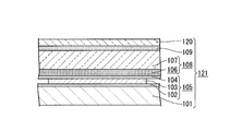
- FIG. 6A is a schematic cross-sectional view showing the configuration of the liquid crystal display device according to the second embodiment of the present invention.
- FIG. 6B is a schematic enlarged view of a portion A in FIG. 6A.
- the scale of each member is appropriately changed to make each member a recognizable size.
- a liquid crystal display device 150 includes a liquid crystal panel 113 (an image display element using liquid crystal) and an illumination device 112 according to the second embodiment.
- the liquid crystal panel 113 is an image display element that displays an image by controlling a transmitted light by driving a liquid crystal shutter corresponding to a pixel based on an image signal input from a signal source (not shown).
- the illuminating device 112 is an apparatus portion that is disposed on the back surface of the liquid crystal panel 113 and constitutes a backlight that supplies illumination light that illuminates the liquid crystal panel 113.
- a plurality of pixels that can independently emit light are provided. Have. These pixels are pixel-driven based on a control signal such as an image signal sent to a drive unit (not shown), and the driven pixels emit light. With such pixel driving, for example, the illumination device 112 can change the illumination range or change the color of the illumination light based on the control signal.
- the configuration of the main part of the lighting device 112 includes an EL element 111 and a glass substrate 110, which are stacked in this order.
- the EL element 111 is a device part that constitutes an illumination light source in the illumination device 112, and has a configuration in which the counter substrate 101, the light emitting structure 105, and the EL element substrate 108 are laminated in this order from the side opposite to the glass substrate 110. Have.
- the counter substrate 101 is a plate-like or sheet-like member that is disposed to face an EL element substrate 108 to be described later and sandwiches a light emitting structure 105 to be described later between the EL element substrate 108.
- the material of the counter substrate 101 can support the light emitting structure 105 with an appropriate mechanical strength, for example, as long as it is a material that can protect the light emitting structure 105 from moisture or the outside air. It is not limited.
- the counter substrate 101 preferably includes a light reflecting layer that reflects light generated by the light emitting structure 105 toward the EL element substrate 108 on any surface perpendicular to the thickness direction. Further, the counter substrate 101 can be formed of a metal material having light reflectivity. In this case, the counter substrate 101 itself constitutes a light reflection layer.
- the light emitting structure 105 includes a counter electrode 102 disposed on the counter substrate 101, a transparent electrode 104 disposed on the surface of the EL element substrate 108 facing the counter substrate 101, and between the counter electrode 102 and the transparent electrode 104. And the light emitting layer 103 sandwiched between the layers. In the light emitting structure 105, the light emitting layer 103 emits EL by applying a voltage to the transparent electrode 104 and the counter electrode 102 constituting the electrode pair. As the configuration of the light emitting structure 105, various conventionally known configurations can be employed.
- the polarities of the counter electrode 102 and the transparent electrode 104 are not particularly limited, in the second embodiment, since the light generated in the light emitting layer 103 is emitted toward the EL element substrate 108, at least the transparent electrode 104 has a good light transmission property. It is necessary to make an electrode having a property.
- suitable materials for the transparent electrode 104 include, for example, ITO (indium tin oxide, refractive index 1.7 to 2.3), IZO (registered trademark, indium zinc, refractive index 1.9 to 2.4), and the like. Examples can be given.
- ITO indium tin oxide, refractive index 1.7 to 2.3
- IZO registered trademark, indium zinc, refractive index 1.9 to 2.4
- the transparent electrode 104 is preferably an anode.
- the physical quantity with respect to a wavelength of 550 nm is represented unless otherwise specified.
- the material of the counter electrode 102 since the presence or absence of the light-transmitting property and the level of the counter electrode 102 are not limited, an appropriate metal material having good conductivity, for example, aluminum, silver, copper, or the like can be used.
- the material of the counter electrode 102 is preferably a material having high reflectance.
- the same material as the transparent electrode 104 should be used as the material of the counter electrode 102. Is also possible.
- the light emitting layer 103 can be, for example, a white light emitting layer.
- the transparent electrode 104 is formed of ITO
- the counter electrode 102 is formed of aluminum
- CuPc (copper phthalocyanine) / ⁇ -NPD is doped with 1% rubrene / gena from the transparent electrode 104 toward the counter electrode 102.
- a configuration in which perylene 1% doped / Alq 3 / lithium fluoride is laminated on octylanthracene in this order can be employed.
- the structure of the light-emitting layer 103 is not limited to this, and the wavelength of light emitted from the light-emitting layer 103 can be set to wavelengths indicating R (red), G (green), and B (blue) as appropriate. Any configuration using materials can be employed.
- the illumination device 112 is pixel driven, the light emitting structure 105 is formed corresponding to each pixel, and the transparent electrode 104 and the counter electrode 102 of each pixel are provided in a driving unit (not shown). Wired. That is, although only the configuration of one pixel is shown in FIG. 6A, another pixel is configured between the counter substrate 101 and the EL element substrate 108, adjacent to the illustrated light emitting structure 105.
- a plurality of light emitting structures 105 are arranged.
- the arrangement pattern of the plurality of light emitting structures 105 is not particularly limited. For example, an arrangement pattern such as a rectangular lattice shape in plan view is possible.
- the EL element substrate 108 protects the light emitting structure 105 by covering the light emitting structure 105 from the side opposite to the counter substrate 101, and transmits light generated in the light emitting layer 103 and transmitted through the transparent electrode 104 to the outside. It is a translucent plate-shaped member for taking out.
- EL device substrate 108, the transparent substrate 107 having a lower refractive index n T than the refractive index n E of the transparent electrode 104 is formed by laminating on a transparent substrate 107, And a light scattering layer 106 disposed in close contact with the surface of the transparent electrode 104 opposite to the light emitting layer 103.
- the light scattering layer 106 makes it difficult for total reflection at the interface between the light scattering layer 106 and the transparent electrode 104 and total reflection at the interface between the light scattering layer 106 and the translucent substrate 107.
- the light scattering layer 106 is a light-transmitting layered portion provided to improve the light transmittance from the transparent electrode 104 to the light-transmitting substrate 107 with respect to the light generated in the light emitting structure 105.
- the light scattering layer 106 includes a base material portion 106B and scattering particles 106A.
- the base material portion 106B is a portion in which the refractive index is adjusted to a constant value nBH by blending the refractive index adjusting particles 106b having light transmittance and the binder 106a.
- the refractive index n BH is such that the light generated in the light emitting structure 105 is totally reflected at at least one of the interface between the light scattering layer 106 and the transparent electrode 104 and the interface between the light scattering layer 106 and the translucent substrate 107.
- the value is set appropriately as it becomes difficult to reflect (including the case where it is not totally reflected).
- the refractive index n BH is equal to or lower than the refractive index n T of the translucent substrate 107, total reflection does not occur at the interface of the translucent substrate 107, but the interface between the light scattering layer 106 and the transparent electrode 104. In this case, total reflection is more likely to occur than when the light scattering layer 106 is not provided. For this reason, the refractive index n BH needs to be set to a refractive index higher than at least the refractive index of the translucent substrate 107.
- the refractive index n BH can be set to an intermediate size between the refractive index n E of the transparent electrode 104 and the refractive index n T of the translucent substrate 107.
- n BH is from 1.60. Largely less than 1.90 is preferable, and 1.70 or more and less than 1.90 is more preferable.
- total reflection at the interface between the light scattering layer 106 and the translucent substrate 107 is reduced as compared with the case where the scattering particles 106A are not provided due to the action of the scattering particles 106A described later.
- the refractive index difference (n E ⁇ n BH ) is small so that the refractive index n BH is close to the refractive index n E of the transparent electrode 104.
- the refractive index difference (n E ⁇ n BH ) is more preferably in the range of greater than 0 and 0.15 or less.
- the material of the binder 106a and the refractive index adjusting particles 106b is not particularly limited as long as a layered portion having a refractive index nBH can be formed.
- a low refractive index material is used as the binder 106a, and the amount of refractive index adjusting particles 106b made of a material with a higher refractive index is adjusted to change the refractive index. It is preferable to adjust n BH .
- Examples of a material suitable for the binder 106a may be either an ionizing radiation curable resin or a thermosetting resin.
- the resin material include an acrylic resin, a polyester resin, a polycarbonate resin, a styrene resin, and an acrylic resin. / Styrene copolymer resin.
- ultraviolet rays are used as ionizing radiation when the resin is cured, a photopolymerization initiator is added to the hard coat layer forming coating solution.
- a known photopolymerization initiator can be used as the photopolymerization initiator, but it is preferable to use a photopolymerization initiator suitable for a material for forming the binder 106a (hereinafter referred to as a binder matrix forming material).
- benzoin such as benzoin, benzoin methyl ether, benzoin ethyl ether, benzoin isopropyl ether, benzyl methyl ketal, and alkyl ethers thereof can be used.
- the amount of the photopolymerization initiator used is preferably from 0.5 to 20 parts by weight, more preferably from 1 to 5 parts by weight, based on the binder matrix-forming material.
- suitable materials for the refractive index adjusting particles 106b include, for example, zirconia oxide (refractive index 2.4), titanium oxide (refractive index 2.52, 2.71), and zinc oxide (refractive index 1.95). And metal oxides such as Among these, zirconia oxide and titanium oxide are particularly preferable as the material for the refractive index adjusting particle 106b in view of high refractive index, chemical stability, low light absorption in the visible light region, and particle size.
- the refractive index adjusting particle 106b one kind of the above particles may be used, or a mixed particle in which two or more kinds are mixed may be used.
- the scattering particles 106A are members that scatter light incident on the base material portion 106B, and are formed of a transparent material having a refractive index n A different from the refractive index n BH of the base material portion 106B. Are distributed.
- suitable materials for the scattering particles 106A include inorganic particles such as silica, alumina, and titanium oxide, and organic particles such as silicone, melamine, and acryl / styrene copolymer particles.
- the scattering particles 106A dispersed in the base material portion 106B particles of one type of material may be used, or particles of two or more types of materials may be mixed and used.
- composition of the light-scattering layer 106, a weight ratio W H refractive index adjusting particles 106b to binder 106a, and the weight ratio W A of the scattering particles 106A to binder 106a a composition satisfying the following formula (1).
- the refractive index in the base material portion 106B is set. Since the content of the adjusting particles 106b becomes too small, a refractive index n BH suitable as the base material portion 106B cannot be obtained. As a result, the difference between the refractive index n BH of the base material portion 106B and the refractive index of the transparent electrode 104 becomes too large, and total reflection at the interface between the base material portion 106B and the transparent electrode 104 cannot be reduced. .
- the scattering particles 106 ⁇ / b> A aggregate and are dispersed in the base material portion 106 ⁇ / b> B in a lump state.
- the scattering particles 106 ⁇ / b> A aggregated into a lump in this way have a large cross-sectional area, and as a result, the light component reflected by the transparent electrode 104 increases, resulting in a decrease in the transmittance of the light scattering layer 106.
- W H / W A is more preferably in a narrower range than the range of the formula (1).
- a more preferable range of W H / W A is 4 or more and 7 or less.
- the refractive index n A of the scattering particle 106A and the refractive index n BH of the base material portion 106B satisfy the following formula (2).
- the refractive index adjusting particles 106b are preferably polydisperse particles having a particle size RH distributed in a range of 1 nm to 300 nm, and the scattering particles 106A are formed of the light scattering layer 106.
- the average particle diameter RA is preferably monodisperse particles satisfying the following formula (2).
- the refractive index adjusting particles 106b can be further improved in dispersibility by setting the particle size RH in the range of 10 nm to 300 nm. If the refractive index adjusting particle 106b is in the above particle diameter range, the refractive index of the light scattering layer 106 can be appropriately set by appropriately selecting in consideration of dispersibility.
- “monodisperse particles” refers to a group of particles having a narrow particle size distribution with a uniform particle size distribution. Typically, it means that the particle size of the particles is within the range of the average particle size R A ⁇ 1 ⁇ m, more strictly, R A ⁇ 1 ⁇ m ⁇ D10 and D90 ⁇ R A +1 ⁇ m. .
- “polydisperse particles” refers to a group of particles having a wide particle size distribution in which the sizes of the particles are not uniform.
- polydisperse particles mean that the particle size of the particles is wider than the average particle size range R A ⁇ R A ⁇ 0.1 ⁇ m, more precisely D10 ⁇ R A ⁇ R A ⁇ It means that the condition of 0.1 ⁇ m and R A + R A ⁇ 0.1 ⁇ m ⁇ D90 is satisfied.
- D10 and D90 when a position showing a fine particle size in the particle size distribution is defined as zero, and an oversized cumulative distribution that represents a curve that rises to the right is represented, particles that have a cumulative value of 10% The particle diameter is D10, and the particle diameter at which the cumulative value is 90% is D90.
- H / R A When H / R A is less than 1.5, the scattering property is increased because the scattering particles 106A are larger than the film thickness of the light scattering layer 106. For this reason, the transmittance as the light scattering layer 106 tends to be lowered. When H / R A exceeds 20, since the scattering particles 106A are small relative to the film thickness of the light scattering layer 106, the scattering property is weakened. For this reason, the light extraction efficiency as the EL element 111 tends to decrease.
- a smoothing layer that prevents the scattering particles 106A from protruding and flattens the interface may be provided at a position where the interface between the light scattering layer 106 and the transparent electrode 104 is formed. If the scattering particles 106A are exposed and unevenness occurs at the interface between the light scattering layer 106 and the transparent electrode 104, for example, when the transparent electrode 104 is formed on the light scattering layer 106, the surface of the transparent electrode 104 is There is a possibility that the light scattering layer 106 may be formed in a shape following the unevenness of the surface, or the film thickness of the transparent electrode 104 may be uneven.
- a smoothing layer because such a problem can be surely prevented.
- a resin material having a refractive index close to that of each of the transparent electrode 104 and the light scattering layer 106 can be employed.
- a particularly preferable material is the same material as the base material portion 106 ⁇ / b> B of the light scattering layer 106.
- the translucent substrate 107 is a plate-like or sheet-like member that transmits light transmitted from the light emitting structure 105 through the light scattering layer 106 toward the glass substrate 110.
- the material of the light-transmitting substrate 107 an appropriate light-transmitting material having good transmittance can be used.
- the transmittance of the translucent substrate 107 is preferably 85% or more.
- Examples of materials that can be suitably used for the light-transmitting substrate 107 include polyethylene terephthalate (PET), triacetyl cellulose (TAC), diacetyl cellulose, acetyl cellulose butyrate, polyethylene naphthalate (PEN), cycloolefin polymer, Examples thereof include films of polyimide, polyethersulfone (PES), polymethyl methacrylate (PMMA), polycarbonate (PC) and the like. These materials are preferable in that they each have appropriate transparency, mechanical strength, and refractive index.
- PET polyethylene terephthalate
- TAC triacetyl cellulose
- PEN polyethylene naphthalate
- PEN polyethylene naphthalate
- cycloolefin polymer examples thereof include films of polyimide, polyethersulfone (PES), polymethyl methacrylate (PMMA), polycarbonate (PC) and the like. These materials are preferable in that they each have appropriate transparency, mechanical strength, and refr
- the glass substrate 110 is a translucent member that forms a surface on the light emission side of the lighting device 112.
- the glass substrate 110 is bonded to the surface of the light-transmitting substrate 107 opposite to the light scattering layer 106 via a bonding layer 109 made of a transparent adhesive or adhesive.
- a bonding layer 109 made of a transparent adhesive or adhesive.
- an acrylic adhesive or pressure-sensitive adhesive can be employed.
- a coating liquid in which the refractive index adjusting particles 106b and the scattering particles 106A are dispersed in an uncured binder 106a is prepared. Then, it is applied to the surface of the translucent substrate 107. Next, according to the curing type of the binder 106 a, for example, irradiation with ionizing radiation or heating is performed to cure, and the light scattering layer 106 is formed on the surface of the translucent substrate 107. As a result, the EL element substrate 108 is obtained.
- the transparent electrode 104 is formed on the light scattering layer 106 of the EL element substrate 108, and the light emitting layer 103 and the counter electrode 102 are sequentially formed to form a plurality of light emitting structures 105.
- the counter substrate 101 is disposed with the light emitting structure 105 sandwiched between the counter substrate 101 and the EL element substrate 108, and the light emitting structure 105 is placed on the counter substrate 101 by, for example, laminating. Adhere closely.
- the EL element 111 is formed.
- the glass substrate 110 is bonded to the light-transmitting substrate 107 of the EL element 111 through the bonding layer 109.
- the illuminating device 112 is formed.
- the liquid crystal display device 150 can be manufactured by disposing the glass substrate 110 of such an illuminating device 112 on the back surface of the liquid crystal panel 113 facing the liquid crystal panel 113.
- the operation and action of the liquid crystal display device 150 and the illumination device 112 will be described focusing on the operation and action of the EL element 111.
- a DC voltage is applied between the transparent electrode 104 and the counter electrode 102 from a driving unit (not shown)
- holes are injected from the transparent electrode 104 into the light emitting layer 103 and electrons are transmitted from the counter electrode 102. Injected into the light emitting layer 103. The injected electrons and holes are recombined to generate excitons, and light is emitted from the light emitting layer 103 when the excitons are deactivated.
- the light directed to the transparent electrode 104 is incident on the transparent electrode 104, and the light directed to the counter electrode 102 is reflected by the counter electrode 102 or the counter substrate 101 and then is reflected on the transparent electrode 104. Incident.
- the light incident on the transparent electrode 104 is transmitted through the light scattering layer 106 according to the incident angle.
- the scattering particles 106A are dispersed in the base material portion 106B adjusted to the refractive index n BH by the refractive index adjusting particles 106b.
- the refractive index n BH of the base material portion 106B is higher than the refractive index n T of the translucent substrate 107. For this reason, compared with the case where the translucent substrate 107 is directly laminated on the transparent electrode 104, more light is incident on the light scattering layer 106, and at the interface between the EL element substrate 108 and the transparent electrode 104. Total reflection is reduced.
- the scattering particle 106A When the light that has entered the light scattering layer 106 reaches the scattering particle 106A, it is refracted according to the difference in refractive index between the scattering particle 106A and the base material portion 106B, and passes through the scattering particle 106A or within the scattering particle 106A. After repeating internal reflection at, light is emitted from the scattering particles 106A. Thereby, the light incident on the scattering particle 106A is scattered around the incident direction. In the second embodiment, since W H / W A satisfies the above formula (1), the scattering particles 106A do not aggregate in the base material portion 106B in a state where the refractive index n BH is well adjusted.
- the transparent electrodes 104 are dispersed and separated appropriately in the direction along the electrode surface. For this reason, after entering the light scattering layer 106, the light traveling in the direction of the incident angle less than the critical angle at the interface between the light scattering layer 106 and the translucent substrate 107 has a high probability of passing between the scattering particles 106A. Thus, the light enters the translucent substrate 107 without causing total reflection at the interface between the light scattering layer 106 and the translucent substrate 107.
- the light incident on the scattering particles 106 ⁇ / b> A also has a small cross-sectional area in scattering because the scattering particles 106 ⁇ / b> A do not aggregate, and the light-transmitting substrate 107 is smaller than the amount of light components reflected toward the transparent electrode 104.
- the amount of light components scattered toward the increases.
- the light traveling in the direction of the incident angle exceeding the critical angle at the interface between the light scattering layer 106 and the translucent substrate 107 after entering the light scattering layer 106 has a long process in the light scattering layer 106.
- the probability of entering the scattering particle 106A is increased. Since the light incident on the scattering particle 106A is scattered by the scattering particle 106A, the light component incident at a smaller incident angle with respect to the interface between the light scattering layer 106 and the translucent substrate 107 is remarkably increased.
- the transparent electrode 104 is changed to the light transmitting substrate 107 as compared with the case where the EL element substrate 108 is made of only the light transmitting substrate 107. Incident light quantity increases. The light incident on the light transmitting substrate 107 is emitted to the outside of the EL element 111. For this reason, according to the EL element 111, since the EL element substrate 108 having the light scattering layer 106 is provided, the light extraction efficiency of light incident from the light emitting structure 105 can be improved. Since the illumination device 112 according to the second embodiment includes the EL element 111 having such a high light extraction efficiency, it is possible to reduce power consumption when forming illumination light.
- the EL element 111 according to the second embodiment further achieves better light extraction efficiency by satisfying the above formula (2) or the above formula (3).
- FIG. 7 is a schematic cross-sectional view showing a configuration of a liquid crystal display device of a first modification according to the second embodiment of the present invention.
- the liquid crystal display device 151 of the present modification includes an EL element 111 similar to that of the second embodiment, instead of the illumination device 112 in the liquid crystal display device 150 according to the second embodiment. . That is, the liquid crystal display device 151 has a configuration in which the bonding layer 109 and the glass substrate 110 are deleted from the liquid crystal display device 150 according to the second embodiment.
- the EL element 111 of this modification is disposed on the back surface of the liquid crystal panel 113 and constitutes a backlight that supplies illumination light that irradiates the liquid crystal panel 113. For this reason, this modification is an example in which the EL element 111 itself is used as a lighting device.
- the liquid crystal display device 151 includes the EL element 111 as an illumination light source as in the second embodiment, the liquid crystal display device 151 has the same effect as that in the second embodiment.
- FIG. 8 is a schematic cross-sectional view showing a configuration of a second modification of the EL element according to the second embodiment of the present invention.
- the EL element 121 of this modification has a configuration in which a counter substrate 101, a light emitting structure 105, and an EL element substrate 108 similar to those in the second embodiment are stacked in this order. Further, a barrier film 120 is laminated on the light transmitting substrate 107 with a bonding layer 109 interposed therebetween. That is, the EL element 121 has the same configuration as that of the substrate including the barrier film 120 instead of the glass substrate 110 of the illumination device 112 according to the second embodiment.
- the EL element 121 of this modification can also be used as an illumination device such as a backlight. For example, in the liquid crystal display device 150 according to the second embodiment, it can be used in place of the illumination device 112.
- the EL element 121 can be driven in the same manner as the EL element 111, the EL element 121 can be used as a display device using the EL element 121 itself as a display portion.
- a description will be given centering on differences from the second embodiment.
- the barrier film 120 is a sheet-like member that constitutes the surface of the EL element 121 opposite to the counter substrate 101 and protects the light emitting structure 105 from moisture, outside air, and the like. It has translucency.
- the transmittance of the barrier film 120 is preferably 85% or more, and the refractive index of the barrier film 120 is preferably close to the refractive index of the light scattering layer 106.
- Examples of the barrier film 120 include a film formed by depositing silicon oxide, alumina, or the like on a base material such as PET by vapor deposition, sputtering, or the like.
- the EL element 121 having such a configuration, since the EL element substrate 108 is provided, the light extraction efficiency can be improved similarly to the EL element 111 according to the second embodiment.
- the EL element 121 can have flexibility as a whole of the EL element 121 by configuring the counter substrate 101 and the light-transmitting substrate 107 with a material having a possibility similar to the barrier film 120. According to such an EL element 121, a curved display surface or illumination surface can be formed.
- the glass substrate 110 is limited to flat glass.
- an optical sheet on which an appropriate lens, a diffusion layer, or the like for condensing or diffusing light is formed, or a structure in which such an optical sheet is laminated on the glass substrate 110 can be used. .
- the EL element 111 according to the second embodiment can be used as a display device using the EL element 111 itself as a display unit, similarly to the EL element 121 of the second modification.
- the illumination device 112 according to the second embodiment can also be used as a display device that displays an image or the like by pixel driving the EL element 111.
- Examples 1 to 6 corresponding to the EL element 111 according to the second embodiment will be described together with Comparative Examples 1 to 4.
- the configuration of the counter substrate 101, the light emitting structure 105, and the light transmitting substrate 107 is the same, and corresponds to the light scattering layer 106 and the light scattering layer 106. Only the structure of the layered portion (hereinafter, these may be simply referred to as a light scattering layer) is different.
- Table 1 below shows the manufacturing conditions of the light scattering layers of Examples 1 to 6 and Comparative Examples 1 to 4.
- Example 1 The EL element 111 of Example 1 was manufactured as follows.
- A4300 (trade name; manufactured by Toyobo Co., Ltd.), which is a polyethylene terephthalate film having a thickness of 125 ⁇ m, was used.
- the transmittance of A4300 is 92.3%, and the refractive index n T is 1.60.
- an acrylic UV curable resin manufactured by Kyoeisha Chemical Co., Ltd. having a refractive index of 1.52 which becomes the binder 106a during curing, and a photopolymerization initiator (Manufactured by BASF), zirconia dispersion (manufactured by Solar Co., Ltd.) as high refractive index fine particles as refractive index adjusting particles 106b, and acrylic / styrene copolymer (manufactured by Soken Chemical Co., Ltd.) as scattering particles 106A did.
- the above materials were appropriately blended to form a coating liquid # 1.
- the fine particles to be measured are immersed in a dispersion having a different refractive index, and when the scattered light from the fine particles in the dispersion becomes invisible by irradiating light, the refractive index is defined as the refractive index of the fine particles. This is a measurement method.
- the coating liquid # 1 was applied to the surface of the translucent substrate 107 with a slot die coater, and the solvent contained in the coating liquid # 1 was evaporated. Thereafter, the coating liquid # 1 was cured by irradiating ultraviolet rays of 400 mJ / cm 2 in an atmosphere having an oxygen concentration of 0.03% or less using a high-pressure mercury lamp. Thereby, a light scattering layer 106 having a thickness H of 7 ⁇ m was formed. In this way, an EL element substrate 108 of Example 1 was obtained.
- the film thickness H of the light-scattering layer 106 is a specified portion uniformly distributed over the entire effective surface area in accordance with JIS-K5600-1999 using an electronic micrometer (Digimicro MU-501A manufactured by Nikon). The local film thickness was measured to determine the average film thickness.
- the effective surface area was 0.1 m square, and the specified number of locations was 10.
- Example 2 to 6 In Examples 2 to 6, the types of the binder 106a and the refractive index adjusting particles 106b are the same as in Example 1 described above, and only the refractive index and the particle diameter of the scattering particles 106A are changed. Different coating liquids # 2 to # 6 were prepared by changing the blending amounts, and the EL element substrate 108 and the EL element 111 were manufactured by changing the film thickness of the light scattering layer 106 as necessary.
- the light scattering layer 106 of H 6 ( ⁇ m) was formed by applying and curing on the light-sensitive substrate 107, which is different from Example 1.
- n BH 1.78.
- n BH 1.60.
- n BH 1.60.
- n BH 1.62.
- the light scattering layer 106 with H 4 ( ⁇ m) was formed by applying and curing on the light-emitting substrate 107, which is different from Example 1.
- n BH 1.71.
- Comparative Examples 1 to 4 In Comparative Examples 1 to 4, the types of the binder 106a and the refractive index adjusting particles 106b are the same as those in Example 1 described above, and only the refractive index and the particle diameter of the scattering particles 106A are changed. Different coating liquids # 7 to # 10 were prepared by changing the blending amount, and the thickness of the light scattering layer was changed to produce a substrate for EL element and an EL element of Comparative Example.
- the total luminous flux when the EL element of each example and each comparative example was caused to emit light and the total luminous flux of the comparative EL element from which the light scattering layer was removed were measured.
- Relative evaluation was performed based on the increase rate of the luminous flux with respect to the total luminous flux of the EL element.
- the total luminous flux was measured using an LMS-400 (trade name; manufactured by labsphere), which is a total luminous flux measuring instrument using an integrating sphere.
- the evaluation results are shown in the “efficiency” column of Table 2 where “ ⁇ ” (excellent, very good) when the increase rate of the luminous flux is 20% or more, “ ⁇ ” (good, good) When less than 5%, it was described as “x” (bad, no good).
- the transmittance of the light scattering layer was determined by the difference between the transmittance of the substrate for EL element of each example and each comparative example and the transmittance of the translucent substrate 107.
- a spectrophotometer U-4100 (trade name; manufactured by Hitachi High-Technologies Corporation) was used. The evaluation result is “ ⁇ ” (good, good) when the transmittance is 80% or more, and “ ⁇ ” (bad, no good) when the transmittance is less than 80%. Described.
- the aggregation state of the scattering particles in the light scattering layer was evaluated by observing the light scattering layer of the EL element substrate of each example and each comparative example using an optical microscope MX50T-877MD (trade name; manufactured by Olympus). The evaluation results are indicated in the “aggregation” column of Table 2 as “ ⁇ ” (good, good) when no aggregation is confirmed, and “x” (bad, no good) when aggregation is confirmed.
- Table 2 shows the calculated values of various quantities corresponding to the above formulas (1) to (3), and each example and each comparative example satisfy the above formulas (1) to (3). , “ ⁇ ” (good), and “ ⁇ ” (bad) when not satisfied.
- Examples 1 to 3 and 6 are examples that satisfy all of the above formulas (1) to (3).
- Examples 4 and 5 are examples that satisfy the expressions (1) and (2).
- Comparative Examples 1, 2, and 4 are examples that do not satisfy the above formula (1).
- Comparative Example 3 is an example that does not satisfy the expressions (1) and (2).
Landscapes
- Physics & Mathematics (AREA)
- Optics & Photonics (AREA)
- Nonlinear Science (AREA)
- Chemical & Material Sciences (AREA)
- General Physics & Mathematics (AREA)
- Mathematical Physics (AREA)
- Crystallography & Structural Chemistry (AREA)
- Dispersion Chemistry (AREA)
- Electroluminescent Light Sources (AREA)
Abstract
本発明のEL素子(10、20、111、121)は、透明電極(4、104)、発光層(3、103)、及び対向電極(2、102)がこの順に積層されたEL発光部(5、105)と、凹凸形状を有するとともに前記発光層(3、103)で発生した光を外部に出射する光学シート(9)が表面に配置された透光性基板(107)と、光散乱層(6、106)とを備える。光散乱層(6、106)は、光散乱粒子(16A、16B)を含んで構成され、前記光散乱粒子(16A、16B)によって構成される凝集体(17)により凹凸形状が形成されているとともに前記EL発光部(5、105)の前記透明電極(4、104)に向いた第1表面(6a)と、密集状態の前記光散乱粒子(16A、16B)が前記第1表面の前記凹凸形状に比べて滑らかな面に沿って整列しているとともに前記透光性基板(107)に向いた第2表面(6b)とを有し、前記EL発光部(5、105)と前記透光性基板(107)との間に配置されている。
Description
本発明は、EL素子(エレクトロ・ルミネッセンス素子)、EL素子用基板、照明装置、ディスプレイ装置、及び液晶ディスプレイ装置に関する。
本願は、2014年3月14日に日本に出願された特願2014-051963号及び2014年3月14日に日本に出願された特願2014-051964号に基づき優先権を主張し、その内容をここに援用する。
本願は、2014年3月14日に日本に出願された特願2014-051963号及び2014年3月14日に日本に出願された特願2014-051964号に基づき優先権を主張し、その内容をここに援用する。
従来、例えば、照明装置、ディスプレイ装置、液晶ディスプレイ装置における表示部や光源(表示用光源)、あるいは照明用光源として、EL素子を用いた装置が知られている。
このようなEL素子として、例えば、蛍光有機化合物を含む発光層を陽極と陰極との間に挟んだ発光構造が知られている。この発光構造が透光性基板の片面上に設けられた構成を有する有機EL素子が用いられることが多い。
このような有機EL素子においては、陽極と陰極の間に直流電圧を印加し、発光層に電子及び正孔を注入して再結合させることにより励起子を生成し、この励起子が失活する際の光の放出を利用して有機EL素子は発光する。このため、発光構造体を構成する電極は、少なくとも光取り出し側の電極が透明電極で構成される。一般には、透光性基板上に設けられた陽極が透明電極で形成され、発光層から出射された光は、この透明電極と透光性基板とを通して外部に出射される。
しかし、このようなEL素子では、発光層から放出された光が透光性基板から外部に射出する際に、一部の光が透光性基板の表面上で全反射されてしまい(一部の光が透光性基板と透明電極との界面で全反射してしまい)、この光は外部に出射されず、内部反射を繰り返すうちに減衰する。これにより、光量損失が生じるという問題があった。この場合、このような光量損失が発生するEL素子における光の外部取り出し効率は(以下、光取り出し効率という)は、一般に20%程度と言われている。
このようなEL素子として、例えば、蛍光有機化合物を含む発光層を陽極と陰極との間に挟んだ発光構造が知られている。この発光構造が透光性基板の片面上に設けられた構成を有する有機EL素子が用いられることが多い。
このような有機EL素子においては、陽極と陰極の間に直流電圧を印加し、発光層に電子及び正孔を注入して再結合させることにより励起子を生成し、この励起子が失活する際の光の放出を利用して有機EL素子は発光する。このため、発光構造体を構成する電極は、少なくとも光取り出し側の電極が透明電極で構成される。一般には、透光性基板上に設けられた陽極が透明電極で形成され、発光層から出射された光は、この透明電極と透光性基板とを通して外部に出射される。
しかし、このようなEL素子では、発光層から放出された光が透光性基板から外部に射出する際に、一部の光が透光性基板の表面上で全反射されてしまい(一部の光が透光性基板と透明電極との界面で全反射してしまい)、この光は外部に出射されず、内部反射を繰り返すうちに減衰する。これにより、光量損失が生じるという問題があった。この場合、このような光量損失が発生するEL素子における光の外部取り出し効率は(以下、光取り出し効率という)は、一般に20%程度と言われている。
このように光取り出し効率が低いと、必要な輝度を得るために、より多くの投入電力が必要となる。また、投入電力が増大されることで、EL素子に対する負荷が増大して素子自体の信頼性を低下させることにもなる。
このような問題に関し、EL素子における光取り出し効率を向上させる目的で透光性基板に微細な凹凸を形成し、全反射することでロスしている光線の一部を外部に取り出すようにしたEL素子が提案されている。例えば、特許文献1には、透光性基板の一方の面に複数のマイクロレンズエレメントを平面的に配列してなるマイクロレンズアレイを形成することが提案されている。
このような問題に関し、EL素子における光取り出し効率を向上させる目的で透光性基板に微細な凹凸を形成し、全反射することでロスしている光線の一部を外部に取り出すようにしたEL素子が提案されている。例えば、特許文献1には、透光性基板の一方の面に複数のマイクロレンズエレメントを平面的に配列してなるマイクロレンズアレイを形成することが提案されている。
また、上述したようなEL素子を高輝度で発光させると、高駆動電流を要するため、EL素子に対する負荷が増大する結果、EL素子自体が劣化してしまうおそれがあった。
このため、電極、EL層、高屈折率層、及び透光体がこの順に配置されてなるEL素子において、高屈折率層及び透光体のそれぞれの光取り出し面側に、光散乱機能を有する層を設けることが提案されている(例えば、特許文献2参照)。
特許文献2には、高屈折率層の光取り出し面側の光散乱機能を有する層として、透明樹脂マトリックスに屈折率差を有する透明粒子を分散させた構成が記載されている。
このため、電極、EL層、高屈折率層、及び透光体がこの順に配置されてなるEL素子において、高屈折率層及び透光体のそれぞれの光取り出し面側に、光散乱機能を有する層を設けることが提案されている(例えば、特許文献2参照)。
特許文献2には、高屈折率層の光取り出し面側の光散乱機能を有する層として、透明樹脂マトリックスに屈折率差を有する透明粒子を分散させた構成が記載されている。
しかしながら、上記のような従来技術には、以下のような問題があった。
特許文献1に記載の技術のように、透光性基板の表面にマイクロレンズエレメントを設ける場合、マイクロレンズエレメントへの入射角によっては、発光層側に反射される光成分がある。このような光成分はEL素子の内部に戻ることにより光量損失を起こしやすいという問題がある。
したがって、特許文献1に記載の技術では、マイクロレンズエレメントを有しない場合に比べれば、光取り出し効率を向上できるが、さらに光取り出し効率を向上することが強く求められていた。
特許文献1に記載の技術のように、透光性基板の表面にマイクロレンズエレメントを設ける場合、マイクロレンズエレメントへの入射角によっては、発光層側に反射される光成分がある。このような光成分はEL素子の内部に戻ることにより光量損失を起こしやすいという問題がある。
したがって、特許文献1に記載の技術では、マイクロレンズエレメントを有しない場合に比べれば、光取り出し効率を向上できるが、さらに光取り出し効率を向上することが強く求められていた。
更に、特許文献2の場合、発光構造体に用いられる透明電極の屈折率は、一般的な透明樹脂やガラスなどの屈折率に比べて高い。このため、透明電極と隣接する光散乱機能を有する層(以下、光散乱層という)の透明樹脂マトリックスは、透明樹脂マトリックスと透明電極との界面での全反射を抑制するために、透明電極の屈折率に近い高屈折率材料を用いる必要がある。しかし、透明粒子を分散できるような樹脂材料の屈折率は高い物でも透明電極ほどではないため、全反射を低減しにくいという問題がある。
また、光取り出し効率を高めるには、光散乱層における透明粒子の大きさや分布密度を適切に設定する必要がある。しかし散乱に用いる透明粒子は、透明樹脂マトリックスの内部で凝集を起こしやすく、透明粒子の凝集が起こると光散乱性能や透過率に悪影響を与えるため、配合量に制限がある。
このため、光散乱層を用いて、光取り出し効率をより向上させる技術が強く望まれていた。
また、光取り出し効率を高めるには、光散乱層における透明粒子の大きさや分布密度を適切に設定する必要がある。しかし散乱に用いる透明粒子は、透明樹脂マトリックスの内部で凝集を起こしやすく、透明粒子の凝集が起こると光散乱性能や透過率に悪影響を与えるため、配合量に制限がある。
このため、光散乱層を用いて、光取り出し効率をより向上させる技術が強く望まれていた。
本発明は、上記のような問題に鑑みてなされたものであり、光取り出し効率を向上することができるEL素子及びEL素子用基板を提供することを目的とする。
また、本発明は、このようなEL素子を備えることにより、電力消費を低減することができる(省電力性能の向上)、照明装置、ディスプレイ装置、及び液晶ディスプレイ装置を提供することを目的とする。
また、本発明は、このようなEL素子を備えることにより、電力消費を低減することができる(省電力性能の向上)、照明装置、ディスプレイ装置、及び液晶ディスプレイ装置を提供することを目的とする。
本発明の第1態様に係るEL素子は、透明電極、発光層、及び対向電極がこの順に積層されたEL発光部と、凹凸形状を有するとともに前記発光層で発生した光を外部に出射する光学シートが表面に配置された透光性基板と、光散乱粒子を含んで構成され、前記光散乱粒子が凝集した凝集体により凹凸形状が形成されているとともに前記EL発光部の前記透明電極に向いた第1表面と、密集状態の前記光散乱粒子が前記第1表面の前記凹凸形状に比べて滑らかな面に沿って整列しているとともに前記透光性基板に向いた第2表面とを有し、前記EL発光部と前記透光性基板との間に配置された光散乱層と、備える。
本発明の第1態様に係るEL素子においては、前記光散乱層は、前記第1表面における前記凹凸形状を覆う平滑な接合面を形成する光透過性の平滑化層を介して、前記透明電極と接合されてもよい。
本発明の第1態様に係るEL素子は、前記透光性基板において前記光散乱層に向いた表面に、接合層を介して接合された、透光性を有するシート状の基材をさらに備え、前記第2表面に設けられた前記光散乱粒子は、前記基材における前記接合層が設けられた表面と反対側の表面に沿って整列してもよい。
本発明の第1態様に係るEL素子においては、前記第2表面に設けられた前記光散乱粒子は、前記透光性基板における前記光学シートが配置された表面と反対側の表面に沿って整列してもよい。
本発明の第1態様に係るEL素子においては、前記光散乱層の前記光散乱粒子は、前記第1表面における粒子密度に比べて、前記第2表面における粒子密度が高くてもよい。
本発明の第1態様に係るEL素子においては、前記光散乱層の前記光散乱粒子は、前記第1表面における平均粒子径に比べて、前記第2表面における平均粒子径が小さくてもよい。
本発明の第2態様に係る照明装置は、上述した第1態様に係るEL素子を発光部として備える。
本発明の第3態様に係るディスプレイ装置は、上述した第1態様に係るEL素子を備え、前記EL素子の前記EL発光部は、独立に駆動可能な複数の画素を有する。
本発明の第4態様に係る液晶ディスプレイ装置は、液晶を用いた画像表示素子と、画像表示素子の背面に配置された、上述した第1態様に係るEL素子とを備える。
本発明の第5態様に係る液晶ディスプレイ装置は、液晶を用いた画像表示素子と、画像表示素子の背面に配置された、上述した第2態様に係る照明装置とを備える。
本発明の第6態様に係るEL素子用基板は、少なくとも一方が透明電極からなる電極対と前記電極対に挟まれた発光層とを有する発光構造体が配置され、EL素子を形成する。本発明の第6態様に係るEL素子用基板は、透光性基板と、光透過性を有する屈折率調整用粒子と光透過性を有するバインダーとが配合されることにより屈折率が前記透光性基板の屈折率よりも高い一定値に調整された母材部と、前記母材部の屈折率とは異なる屈折率を有する透明材料で形成されて前記母材部の内部に分散された散乱粒子とを有し、前記透光性基板の一方の表面に形成され、前記発光構造体の前記透明電極が配置される光散乱層とを備える。前記バインダーに対する前記屈折率調整用粒子の重量比WHと、前記バインダーに対する前記散乱粒子の重量比WAとが、下記式(1)を満足する。
2≦WH/WA≦9 ・・・(1)
2≦WH/WA≦9 ・・・(1)
本発明の第6態様に係るEL素子用基板においては、前記散乱粒子の屈折率をnA、前記母材部の屈折率をnBHとするとき、下記式(2)を満足してもよい。
0.05≦|nBH-nA|≦0.5 ・・・(2)
0.05≦|nBH-nA|≦0.5 ・・・(2)
本発明の第6態様に係るEL素子用基板においては、前記屈折率調整用粒子は、粒径が1nm以上300nm以下の範囲に分布する多分散粒子であり、前記散乱粒子は、前記散乱粒子の平均粒径をRA、前記光散乱層の膜厚をHとするとき、下記式(3)を満足する単分散粒子であってもよい。
1.5≦H/RA≦20 ・・・(3)
1.5≦H/RA≦20 ・・・(3)
本発明の第7態様に係るEL素子は、上述した第6態様に係るEL素子用基板と、少なくとも一方が透明電極からなる電極対と前記電極対に挟まれた発光層とを有する発光構造体とを備え、前記EL素子用基板の前記透光性基板は、前記透明電極の屈折率よりも低い屈折率を有し、前記発光構造体の前記透明電極は、前記透光性基板と前記透明電極との間に前記EL素子用基板の前記光散乱層を挟むように、前記透光性基板と対向する位置に配置されている。
本発明の第7態様に係るEL素子においては、前記発光構造体は、独立に駆動可能な複数の画素を形成してもよい。
本発明の第8態様に係る照明装置は、上述した第7態様に係るEL素子を照明光源として備える。
本発明の第9態様に係るディスプレイ装置は、上述した第7態様に係るEL素子を表示部として備える。
本発明の第10態様に係る液晶ディスプレイ装置は、液晶を用いた画像表示素子と、前記画像表示素子の背面に照明光源として配置された、上述した第7態様に係るEL素子とを備える。
本発明の第11態様に係る液晶ディスプレイ装置は、液晶を用いた画像表示素子と、前記画像表示素子の背面に配置された、上述した第8態様に係る照明装置とを備える。
本発明の上記態様に係るEL素子によれば、透明電極に向いた第1表面と透光性基板に向いた第2表面とで、光散乱粒子の配置を変えた光散乱層を備えるため、光取り出し効率を向上することができるという効果を奏する。
また、本発明の上記態様に係る照明装置、ディスプレイ装置、及び液晶ディスプレイ装置によれば、本発明の上記態様に係るEL素子を備えるため、省電力性能を向上することができるという効果を奏する。
また、本発明の上記態様に係る照明装置、ディスプレイ装置、及び液晶ディスプレイ装置によれば、本発明の上記態様に係るEL素子を備えるため、省電力性能を向上することができるという効果を奏する。
本発明の上記態様に係るEL素子用基板及びEL素子によれば、光散乱層が、屈折率調整用粒子とバインダーとが配合された透光性基板よりも高い屈折率に調整された母材部と散乱粒子とを有し、バインダーに対する屈折率調整用粒子の重量比WHを、散乱粒子の重量比WAの2倍以上9倍以下にしている。このため、EL素子の発光構造体入射する光の光取り出し効率を向上することができるという効果を奏する。
また、本発明の上記態様に係る照明装置、ディスプレイ装置、及び液晶ディスプレイ装置によれば、本発明の上記態様に係るEL素子を備えることにより電力消費を低減することができるという効果を奏する。
また、本発明の上記態様に係る照明装置、ディスプレイ装置、及び液晶ディスプレイ装置によれば、本発明の上記態様に係るEL素子を備えることにより電力消費を低減することができるという効果を奏する。
以下、図面を参照して本発明を適用した実施形態について詳細に説明する。なお、以下の説明で用いる図面は、本発明の実施形態の構成を説明するためのものであり、図示される各部の大きさや厚さや寸法等は、実際のEL素子、EL素子用基板、照明装置、ディスプレイ装置、及び液晶ディスプレイ装置の寸法関係とは異なる場合がある。
(第1実施形態)
以下では、本発明の第1実施形態について添付図面を参照して説明する。
本発明の第1実施形態に係るEL素子及びEL素子を備える液晶ディスプレイ装置について説明する。
図1は、本発明の第1実施形態に係る液晶ディスプレイ装置及びEL素子の構成を示す模式的な断面図である。図2は、図1におけるA部の模式的な部分拡大図である。図3Aは、図2におけるC部の模式的な部分拡大図である。図3Bは、図2におけるD部の模式的な部分拡大図である。
なお、以下の説明に用いる各図面では、各部材を認識可能な大きさとするため、各部材の縮尺を適宜変更している。
以下では、本発明の第1実施形態について添付図面を参照して説明する。
本発明の第1実施形態に係るEL素子及びEL素子を備える液晶ディスプレイ装置について説明する。
図1は、本発明の第1実施形態に係る液晶ディスプレイ装置及びEL素子の構成を示す模式的な断面図である。図2は、図1におけるA部の模式的な部分拡大図である。図3Aは、図2におけるC部の模式的な部分拡大図である。図3Bは、図2におけるD部の模式的な部分拡大図である。
なお、以下の説明に用いる各図面では、各部材を認識可能な大きさとするため、各部材の縮尺を適宜変更している。
図1に示すように、第1実施形態に係る液晶ディスプレイ装置50は、液晶パネル11(画像表示素子)、及び第1実施形態に係るEL素子10を備える。なお「EL」はエレクトロ・ルミネッセンスを表す。
液晶パネル11は、液晶を用いた画像表示素子であり、詳細構成の図示は省略するが、公知の種々の構成を採用することができる。
液晶パネル11に好適な構成の例としては、例えば、平面視矩形状に配列された画素における光透過率を、偏光板に挟まれた液晶層の偏光状態を画素ごとに独立して制御することにより変化させて、画像表示を行う構成が可能である。この場合、液晶層の偏光状態は、画素ごとに配置された図示略の電極によって、画像信号に応じた電界を印加することにより制御される。
液晶パネル11に好適な構成の例としては、例えば、平面視矩形状に配列された画素における光透過率を、偏光板に挟まれた液晶層の偏光状態を画素ごとに独立して制御することにより変化させて、画像表示を行う構成が可能である。この場合、液晶層の偏光状態は、画素ごとに配置された図示略の電極によって、画像信号に応じた電界を印加することにより制御される。
EL素子10は、第1実施形態では、液晶パネル11の背面に配置され、液晶パネル11を背面から照明するための発光部(発光装置)であり、液晶ディスプレイ装置50における照明装置を構成している。
このため、EL素子10は、均一な照明光を液晶パネル11に照射できればよいが、第1実施形態では、独立に発光可能な複数の発光画素を有している。図1には、一発光画素における構成を示しており、このため、EL素子10では、図示のような構成が、図示の左右方向及び図示奥行き方向に複数隣接して形成されている。
このため、EL素子10は、均一な照明光を液晶パネル11に照射できればよいが、第1実施形態では、独立に発光可能な複数の発光画素を有している。図1には、一発光画素における構成を示しており、このため、EL素子10では、図示のような構成が、図示の左右方向及び図示奥行き方向に複数隣接して形成されている。
EL素子10の概略構成は、対向基板1、発光構造体5(EL発光部)、光散乱層6、透光性基板7、及び光指向性フィルム9がこの順に積層された構成を備える。
発光構造体5は、液晶パネル11に照射する照明光をEL発光によって発生する装置部分である。
第1実施形態では、発光構造体5で発生した光B0は、光散乱層6、透光性基板7、及び光指向性フィルム9を透過して、光B1として外部に出射され、液晶パネル11に照射される。
本明細書において、「透光性」とは、特に断らない限り、発光構造体5で発生した光B0の波長光に関する透光性を意味する。
発光構造体5は、液晶パネル11に照射する照明光をEL発光によって発生する装置部分である。
第1実施形態では、発光構造体5で発生した光B0は、光散乱層6、透光性基板7、及び光指向性フィルム9を透過して、光B1として外部に出射され、液晶パネル11に照射される。
本明細書において、「透光性」とは、特に断らない限り、発光構造体5で発生した光B0の波長光に関する透光性を意味する。
対向基板1及び透光性基板7は、互いの間に発光構造体5及び光散乱層6を挟むため、互いに対向して配置された板状またはシート状の部材である。
対向基板1は、第1実施形態では、EL素子10の厚さ方向に垂直な一方の外表面を形成している。
対向基板1は、特に透光性を必要とはしないため、発光構造体5を積層可能な適宜の材質、例えば、合成樹脂、ガラス、金属などを用いることが可能である。
第1実施形態では、一例として、後述する透光性基板7と同様の材質を採用している。
対向基板1は、第1実施形態では、EL素子10の厚さ方向に垂直な一方の外表面を形成している。
対向基板1は、特に透光性を必要とはしないため、発光構造体5を積層可能な適宜の材質、例えば、合成樹脂、ガラス、金属などを用いることが可能である。
第1実施形態では、一例として、後述する透光性基板7と同様の材質を採用している。
透光性基板7の光透過率は、全光線透過率として、50%以上であることが好ましく、80%以上であることがより好ましい。
透光性基板7に用いる材料としては、種々のガラス材料を用いることができる。この他の材料として、PMMA(ポリメタクリル酸メチル樹脂)、ポリカーボネート、ポリスチレン、PEN(ポリエチレンナフタレート樹脂)、PET(ポリエチレンテレフタレート樹脂)等の合成樹脂材料を用いることができる。
合成樹脂材料を用いる場合、特に好ましい材料はシクロオレフィン系のポリマーである。このポリマーは、加工性及び耐熱性、耐水性、光学透光性等の材料特性の全てにおいて優れた材料である。
透光性基板7に用いる材料としては、種々のガラス材料を用いることができる。この他の材料として、PMMA(ポリメタクリル酸メチル樹脂)、ポリカーボネート、ポリスチレン、PEN(ポリエチレンナフタレート樹脂)、PET(ポリエチレンテレフタレート樹脂)等の合成樹脂材料を用いることができる。
合成樹脂材料を用いる場合、特に好ましい材料はシクロオレフィン系のポリマーである。このポリマーは、加工性及び耐熱性、耐水性、光学透光性等の材料特性の全てにおいて優れた材料である。
発光構造体5は、透明電極4、発光層3、及び対向電極2がこの順に積層され、対向電極2が対向基板1に向いた状態で、対向基板1上に配置されている。
発光構造体5においては、透明電極4と対向電極2とに電圧を印加することにより発光層3が発光する。発光構造体5の構成としては、従来公知のさまざまな構成を採用することができる。
発光構造体5においては、透明電極4と対向電極2とに電圧を印加することにより発光層3が発光する。発光構造体5の構成としては、従来公知のさまざまな構成を採用することができる。
透明電極4は、発光層3に電圧を印加するための一方の電極(第1電極)であり、光B0を透過させることができる材質からなる。このような透光性を有する電極材料としては、例えば、ITO(酸化インジウムスズ)などの例を挙げることができる。
対向電極2は、発光層3に電圧を印加するための他方の電極(第2電極)である。対向電極2の材質は、透明電極4と同様の材質を採用することもできる。しかし、第1実施形態では、対向電極2は透光性の有無や程度は問わないため、対向電極2の材料としては、導電性が良好な適宜の金属材料、例えば、アルミニウム、銀、銅などを採用することもできる。
第1実施形態では、なるべく多くの光B0を光指向性フィルム9から出射するため、対向電極2は、良好な光反射機能を有する材料を採用することが好ましい。対向電極2の光反射率は、50%以上100%以下であることが好ましい。
対向電極2として、光反射率が低いかあるいは透明な材質を用いる場合には、対向電極2から対向基板1までの間に、光反射層を設けることが好ましい。この光反射層は、対向電極2と対向基板1との中間に設けてもよいし、対向基板1あるいは対向電極2に積層して設けたり、対向基板1の内部に設けたりすることも可能である。
また、対向基板1自体を、光反射性の材質で製作することにより、対向基板1が光反射層を兼ねる構成とすることも可能である。
第1実施形態では、なるべく多くの光B0を光指向性フィルム9から出射するため、対向電極2は、良好な光反射機能を有する材料を採用することが好ましい。対向電極2の光反射率は、50%以上100%以下であることが好ましい。
対向電極2として、光反射率が低いかあるいは透明な材質を用いる場合には、対向電極2から対向基板1までの間に、光反射層を設けることが好ましい。この光反射層は、対向電極2と対向基板1との中間に設けてもよいし、対向基板1あるいは対向電極2に積層して設けたり、対向基板1の内部に設けたりすることも可能である。
また、対向基板1自体を、光反射性の材質で製作することにより、対向基板1が光反射層を兼ねる構成とすることも可能である。
透明電極4及び対向電極2の極性は特に限定されないが、第1実施形態では、一例として、透明電極4を陽極、対向電極2を陰極として用いている。
発光層3は、例えば、白色発光層とすることができる。この場合には、透明電極4をITOで形成し、対向電極2をアルミニウムで形成し、透明電極4から対向電極2に向かって、CuPc(銅フタロシアニン)/α-NPDにルブレン1%ドープ/ジナクチルアントラセンにペリレン1%ドープ/Alq3/フッ化リチウムが、この順に積層された構成を採用することができる。
ただし、発光層3の構成は、これに限定されず、発光層3から射出する光線の波長を、R(赤色)、G(緑色)、B(青色)を示す波長に設定することのできる適宜材料を用いた任意の構成を採用することが可能である。
また、液晶ディスプレイ装置50をフルカラーディスプレイ用途で使用する場合には、例えば、発光層3を、R、G、Bに対応した3種類の発光材料に塗り分けた構成や、白色発光層上にカラーフィルターを重ねた構成を採用することができる。
ただし、発光層3の構成は、これに限定されず、発光層3から射出する光線の波長を、R(赤色)、G(緑色)、B(青色)を示す波長に設定することのできる適宜材料を用いた任意の構成を採用することが可能である。
また、液晶ディスプレイ装置50をフルカラーディスプレイ用途で使用する場合には、例えば、発光層3を、R、G、Bに対応した3種類の発光材料に塗り分けた構成や、白色発光層上にカラーフィルターを重ねた構成を採用することができる。
第1実施形態では、EL素子10の発光が発光画素ごとに制御されるため、発光構造体5は、各発光画素に対応して形成され、各発光画素の透明電極4、対向電極2には、図示略の駆動部に配線されている。
光散乱層6は、発光層3で発生し、透明電極4に入射した光を透光性基板7側に透過させるとともに、散乱して光の進行方向を変化させる層状部であり、1種類以上の光散乱粒子を含んで構成される。
光散乱層6は、層厚方向に、光散乱粒子の粒子密度を変えることで、透明電極4から入射する光B0が透過しやすく、透光性基板7を通じて入射する光を透光性基板7に向けて反射しやすくなる構成としている。
具体的には、図2に模式的に示すように、光散乱層6は、第1表面6aと第2表面6bとの間に、第1光散乱層6Aと、第2光散乱層6Bとが形成されている。
図2は模式図のため、第1光散乱層6Aと第2光散乱層6Bとの間に境界面Sを図示しているが、境界面Sに、物理的な界面が形成されることは必須ではない。例えば、第1光散乱層6Aから第2光散乱層6Bに、光散乱粒子の粒子密度が連続的に変化し、物理的な界面が形成されない構成が可能である。
第1実施形態では、境界面Sは、製法上の光散乱粒子の粒子密度を切り替えた境界の位置を示しており、必ずしも物理的な界面にはなっていない。
光散乱層6は、層厚方向に、光散乱粒子の粒子密度を変えることで、透明電極4から入射する光B0が透過しやすく、透光性基板7を通じて入射する光を透光性基板7に向けて反射しやすくなる構成としている。
具体的には、図2に模式的に示すように、光散乱層6は、第1表面6aと第2表面6bとの間に、第1光散乱層6Aと、第2光散乱層6Bとが形成されている。
図2は模式図のため、第1光散乱層6Aと第2光散乱層6Bとの間に境界面Sを図示しているが、境界面Sに、物理的な界面が形成されることは必須ではない。例えば、第1光散乱層6Aから第2光散乱層6Bに、光散乱粒子の粒子密度が連続的に変化し、物理的な界面が形成されない構成が可能である。
第1実施形態では、境界面Sは、製法上の光散乱粒子の粒子密度を切り替えた境界の位置を示しており、必ずしも物理的な界面にはなっていない。
第1光散乱層6Aは、透明電極4に第1表面6aが向くように配置された層状部である。第1実施形態では、第1光散乱層6Aは、平滑化層12を介して透明電極4の表面4aに接合されている。
図3Aに示すように、第1光散乱層6Aは、光散乱粒子16Aがバインダー19A中に分散された構成を有する。
光散乱粒子16Aとしては、例えば、シリカ、アルミナ、酸化チタン、硫酸バリウム等の無機系粒子、アクリル、スチレン、アクリル/スチレン共重合体、メラミン等の有機系粒子、あるいはこれらの粒子から選ばれた2種類以上の粒子を混合した混合粒子を採用することができる。
光散乱粒子16Aの平均粒子径としては、50nm~1000nmが好ましく、100nm~300nmがより好ましい。なお、粒子径は、SALD-7100(商品名;島津製作所製)を用いて測定できる。
第1光散乱層6Aの第1表面6aは、光散乱粒子16Aが塊状に凝集して形成された凝集体17が分布することによって凹凸形状が形成されている。この凹凸形状は、凝集体17により形成されるため、規則性を有しておらず、凹凸ピッチや深さは、ばらついている。第1表面6aの凹凸の大きさとしては、隣接する凹凸の高低差が、0.2μm~3μm程度であることが好ましい。
1つの凸部を形成する凝集体17の粒子数としては、光散乱粒子16Aの粒径分布にもよるが、例えば、2個~10個程度が好ましい。
光散乱粒子16Aとしては、例えば、シリカ、アルミナ、酸化チタン、硫酸バリウム等の無機系粒子、アクリル、スチレン、アクリル/スチレン共重合体、メラミン等の有機系粒子、あるいはこれらの粒子から選ばれた2種類以上の粒子を混合した混合粒子を採用することができる。
光散乱粒子16Aの平均粒子径としては、50nm~1000nmが好ましく、100nm~300nmがより好ましい。なお、粒子径は、SALD-7100(商品名;島津製作所製)を用いて測定できる。
第1光散乱層6Aの第1表面6aは、光散乱粒子16Aが塊状に凝集して形成された凝集体17が分布することによって凹凸形状が形成されている。この凹凸形状は、凝集体17により形成されるため、規則性を有しておらず、凹凸ピッチや深さは、ばらついている。第1表面6aの凹凸の大きさとしては、隣接する凹凸の高低差が、0.2μm~3μm程度であることが好ましい。
1つの凸部を形成する凝集体17の粒子数としては、光散乱粒子16Aの粒径分布にもよるが、例えば、2個~10個程度が好ましい。
第1光散乱層6Aにおいて、光散乱粒子16Aの粒子密度は、第1表面6aから境界面Sに向かうにつれて増大することが好ましい。ただし、後述する第2光散乱層6Bにおける光散乱粒子16Bの粒子密度に比べて低いことが好ましい。
バインダー19Aは、その屈折率が光散乱粒子16Aの屈折率と屈折率差を有する適宜の透明樹脂材料で構成される。
バインダー19Aのバインダーマトリックス材料としては、例えば、電離放射線硬化型または熱硬化型の合成樹脂、例えば、アクリル系樹脂、ポリエステル系樹脂、ポリカーボネート系樹脂、スチレン系樹脂、アクリル/スチレン系の共重合樹脂を使用することができる。
電離放射線として紫外線を用いる場合、バインダーマトリックス材料に光散乱粒子16Aを混合したハードコート層形成用塗液に光重合開始剤が加えられる。光重合開始剤は、公知の光重合開始剤を用いることができるが、用いるバインダーマトリックス形成材料に適した光重合開始剤を用いることが好ましい。
光重合開始剤としては、例えば、ベンゾイン、ベンゾインメチルエーテル、ベンゾインエチルエーテル、ベンゾインイソプロピルエーテル、ベンジルメチルケタールなどのベンゾインとそのアルキルエーテル類等を用いることができる。光重合開始剤の使用量は、バインダーマトリックス形成材料に対して0.5重量部以上20重量部以下である。好ましくは1重量部以上5重量部以下である。
バインダー19Aのバインダーマトリックス材料としては、例えば、電離放射線硬化型または熱硬化型の合成樹脂、例えば、アクリル系樹脂、ポリエステル系樹脂、ポリカーボネート系樹脂、スチレン系樹脂、アクリル/スチレン系の共重合樹脂を使用することができる。
電離放射線として紫外線を用いる場合、バインダーマトリックス材料に光散乱粒子16Aを混合したハードコート層形成用塗液に光重合開始剤が加えられる。光重合開始剤は、公知の光重合開始剤を用いることができるが、用いるバインダーマトリックス形成材料に適した光重合開始剤を用いることが好ましい。
光重合開始剤としては、例えば、ベンゾイン、ベンゾインメチルエーテル、ベンゾインエチルエーテル、ベンゾインイソプロピルエーテル、ベンジルメチルケタールなどのベンゾインとそのアルキルエーテル類等を用いることができる。光重合開始剤の使用量は、バインダーマトリックス形成材料に対して0.5重量部以上20重量部以下である。好ましくは1重量部以上5重量部以下である。
平滑化層12は、第1光散乱層6Aを覆う平滑な接合面12aを形成するとともに、第1光散乱層6Aを透明電極4に接合するための層状部であり、光透過性を有する合成樹脂からなる。
平滑化層12の材質としては、バインダー19Aに好適な上記の合成樹脂のうちから適宜の樹脂材料を選択することが可能である。
ただし、平滑化層12の屈折率は、光B0が表面4aで全反射されないか、または全反射される量を低減できるような屈折率とする。すなわち、平滑化層12の屈折率は、透明電極4の屈折率以上、または透明電極4の屈折率未満の場合に透明電極4の屈折率に近い屈折率を有する。透明電極4の屈折率未満の場合の屈折率差は、0.4以下であることが好ましく、0.2以下であることがより好ましい。
平滑化層12の材質としては、バインダー19Aに好適な上記の合成樹脂のうちから適宜の樹脂材料を選択することが可能である。
ただし、平滑化層12の屈折率は、光B0が表面4aで全反射されないか、または全反射される量を低減できるような屈折率とする。すなわち、平滑化層12の屈折率は、透明電極4の屈折率以上、または透明電極4の屈折率未満の場合に透明電極4の屈折率に近い屈折率を有する。透明電極4の屈折率未満の場合の屈折率差は、0.4以下であることが好ましく、0.2以下であることがより好ましい。
一般に、透明電極4に用いる材料の屈折率は、高屈折率であること多いため、これに応じて平滑化層12を高屈折率化する。このため、上述のバインダー19Aと同様の樹脂材料に屈折率調整用粒子(後述する符号106b)を添加した構成も可能である。
例えば、屈折率調整用粒子としては、例えば、ジルコニア、チタニア、チタン酸カリウム、チタン酸バリウム、酸化亜鉛等の金属酸化物のうち1種を単体で、または2種以上を混合して用いることができる。この中でも特に、ジルコニア及びチタニアは、屈折率が高く、化学的安定性に優れ、可視光域における光の透過率が高く、粒径が揃え易い等の性質を備えるため好ましい。
また、これらの屈折率調整用粒子は、表面が修飾されていてもよい。
また、光散乱層6において、屈折率調整用粒子は、粒径RHが1nm以上300nm以下の範囲に分布する多分散粒子であることが好ましい。一方、光散乱粒子16Aは、単分散性粒子であることが好ましい。なお、屈折率調整用粒子は、粒径RHを10nm以上300nm以下の範囲とすることで、より分散性を高めることができる。
屈折率調整用粒子は、上記粒子径の範囲であれば、分散性を考慮し適宜選択することにより、光散乱層6の屈折率を適切なものとすることができる。
ここで、「単分散性粒子」とは、粒径分布が、ほぼ一定サイズに揃っていて粒径分布が狭い粒子群を言う。典型的には、粒子の粒子径が平均粒径RA±RA×0.5nmの粒径範囲内にあることを意味し、より厳密には、RA-RA×0.5μm≦D10かつ、D90≦RA+RA×0.5μmである。
他方、「多分散粒子」とは、粒子のサイズが揃っていない粒径分布が広い粒子群を言う。典型的には、粒子の典型的には、粒子の粒子径が平均粒径RA±RA×0.1μmの粒径範囲より広いことを意味し、より厳密には、D10≦RA-RA×0.1μmかつ、RA+RA×0.1μm≦D90である。
なお、D10、D90に関し、粒子径分布において細かい粒子径を示す位置をゼロと定義し、かつ、右上がりのカーブとなるオーバーサイズの累積分布が表された場合、累積値が10%となる粒子径がD10であり、累積値が90%となる粒子径がD90である。
例えば、屈折率調整用粒子としては、例えば、ジルコニア、チタニア、チタン酸カリウム、チタン酸バリウム、酸化亜鉛等の金属酸化物のうち1種を単体で、または2種以上を混合して用いることができる。この中でも特に、ジルコニア及びチタニアは、屈折率が高く、化学的安定性に優れ、可視光域における光の透過率が高く、粒径が揃え易い等の性質を備えるため好ましい。
また、これらの屈折率調整用粒子は、表面が修飾されていてもよい。
また、光散乱層6において、屈折率調整用粒子は、粒径RHが1nm以上300nm以下の範囲に分布する多分散粒子であることが好ましい。一方、光散乱粒子16Aは、単分散性粒子であることが好ましい。なお、屈折率調整用粒子は、粒径RHを10nm以上300nm以下の範囲とすることで、より分散性を高めることができる。
屈折率調整用粒子は、上記粒子径の範囲であれば、分散性を考慮し適宜選択することにより、光散乱層6の屈折率を適切なものとすることができる。
ここで、「単分散性粒子」とは、粒径分布が、ほぼ一定サイズに揃っていて粒径分布が狭い粒子群を言う。典型的には、粒子の粒子径が平均粒径RA±RA×0.5nmの粒径範囲内にあることを意味し、より厳密には、RA-RA×0.5μm≦D10かつ、D90≦RA+RA×0.5μmである。
他方、「多分散粒子」とは、粒子のサイズが揃っていない粒径分布が広い粒子群を言う。典型的には、粒子の典型的には、粒子の粒子径が平均粒径RA±RA×0.1μmの粒径範囲より広いことを意味し、より厳密には、D10≦RA-RA×0.1μmかつ、RA+RA×0.1μm≦D90である。
なお、D10、D90に関し、粒子径分布において細かい粒子径を示す位置をゼロと定義し、かつ、右上がりのカーブとなるオーバーサイズの累積分布が表された場合、累積値が10%となる粒子径がD10であり、累積値が90%となる粒子径がD90である。
このような平滑化層12を介して、透明電極4に第1光散乱層6Aを接合することにより、透明電極4を透過して、表面4aに到達した光B0は、略全反射されることなく(すべて全反射される場合も含む)平滑化層12に入射して、第1表面6aに到達する。
また、平滑化層12を備えることにより、透明電極4を平滑な接合面12a上に形成することができるため、透明電極4の層厚のバラツキを抑制することができる。
例えば、第1表面6a上に、直に透明電極4を形成すると、第1表面6aの凹凸形状に応じて、透明電極4の層厚にバラツキが生じる。透明電極4の層厚がばらつくと、輝度ムラが生じたり、電流のショートが発生したりする問題が生じる可能性があるが、第1実施形態ではこれらの発生を防止できる。
また、平滑化層12を備えることにより、透明電極4を平滑な接合面12a上に形成することができるため、透明電極4の層厚のバラツキを抑制することができる。
例えば、第1表面6a上に、直に透明電極4を形成すると、第1表面6aの凹凸形状に応じて、透明電極4の層厚にバラツキが生じる。透明電極4の層厚がばらつくと、輝度ムラが生じたり、電流のショートが発生したりする問題が生じる可能性があるが、第1実施形態ではこれらの発生を防止できる。
第2光散乱層6Bは、図3Bに示すように、境界面Sにおいて第1光散乱層6Aと積層され、透光性基板7に第2表面6bが向くように配置された層状部である。第1実施形態では、図2に示すように、第2光散乱層6Bは、基材13に積層された状態で、接合層14を介して透光性基板7の入射側表面7aに接合されている。
図3Bに示すように、第2光散乱層6Bは、光散乱粒子16Bがバインダー19B中に分散された構成を有する。
光散乱粒子16Bとしては、上述した光散乱粒子16Aに好適な粒子材料のうちから適宜の1種以上の粒子材料を選択することができる。光散乱粒子16Bの種類は、光散乱粒子16Aと同じでもよいし、異なっていてもよい。
光散乱粒子16Bの平均粒子径は、光散乱粒子16Aと同様の平均粒子径を採用することが可能である。ただし、後述する層状整列部18を形成する一つの方法として、光散乱粒子16Bの平均粒径を小径にする場合には、光散乱粒子16Aよりも平均粒子径が小さい光散乱粒子16Bを採用することもできる。
このため、光散乱粒子16Bの平均粒子径としては、例えば、50nm~300nmが好ましく、50nm~150nmがより好ましい。
光散乱粒子16Bとしては、上述した光散乱粒子16Aに好適な粒子材料のうちから適宜の1種以上の粒子材料を選択することができる。光散乱粒子16Bの種類は、光散乱粒子16Aと同じでもよいし、異なっていてもよい。
光散乱粒子16Bの平均粒子径は、光散乱粒子16Aと同様の平均粒子径を採用することが可能である。ただし、後述する層状整列部18を形成する一つの方法として、光散乱粒子16Bの平均粒径を小径にする場合には、光散乱粒子16Aよりも平均粒子径が小さい光散乱粒子16Bを採用することもできる。
このため、光散乱粒子16Bの平均粒子径としては、例えば、50nm~300nmが好ましく、50nm~150nmがより好ましい。
また、バインダー19Bは、その屈折率が光散乱粒子16Bの屈折率と屈折率差を有する適宜の透明樹脂材料で構成される。具体的には、上述したバインダー19Aに好適な材料のうちから、光散乱粒子16Bの屈折率に応じて、適宜の樹脂材料を選択して用いることができる。バインダー19Bの種類は、バインダー19Aと同じでもよいし、異なっていてもよい。
図2に示すように、基材13は、光散乱層6を積層して、シート状の組立体15を形成するシート状部材である。
基材13の材質としては、透光性を有する樹脂フィルムを採用することができる。例えば、セルローストリアセテート、ポリエステル、ポリアミド、ポリイミド、ポリプロピレン、ポリメチルペンテン、ポリ塩化ビニル、ポリビニルアセタール、ポリメタアクリル酸メチル、ポリカーボネート、ポリウレタン等の熱可塑性樹脂からなる延伸フィルムまたは未延伸フィルムを採用することができる。
基材13の透過率としては、例えば、90%以上であることが好ましい。
基材13の材質としては、透光性を有する樹脂フィルムを採用することができる。例えば、セルローストリアセテート、ポリエステル、ポリアミド、ポリイミド、ポリプロピレン、ポリメチルペンテン、ポリ塩化ビニル、ポリビニルアセタール、ポリメタアクリル酸メチル、ポリカーボネート、ポリウレタン等の熱可塑性樹脂からなる延伸フィルムまたは未延伸フィルムを採用することができる。
基材13の透過率としては、例えば、90%以上であることが好ましい。
接合層14は、接合層14を透光性基板7に接合することができ、透光性を有する適宜の粘着剤または接着剤を採用することができる。
接合層14として好適な材料としては、例えば、アクリル系、ウレタン系、ゴム系、シリコーン系等の各種の粘着剤、接着剤が挙げられる。
いずれの場合も、接合層14は、高温となる発光構造体5に隣接されているため、100℃で貯蔵弾性率G’が1.0×10+4(Pa)程度以上である接合層を用いることが望ましい。
貯蔵弾性率G’が上記値よりも低いと、使用中に基材13と透光性基板7との間に位置ずれが生じてしまう可能性がある。このような位置ずれは、発光構造体5の発光画素と、光指向性フィルム9との間の位置ずれにつながり、このような位置ずれは、後述する光指向性フィルム9による光取り出し効率の低下につながるおそれがある。
接合層14として好適な材料としては、例えば、アクリル系、ウレタン系、ゴム系、シリコーン系等の各種の粘着剤、接着剤が挙げられる。
いずれの場合も、接合層14は、高温となる発光構造体5に隣接されているため、100℃で貯蔵弾性率G’が1.0×10+4(Pa)程度以上である接合層を用いることが望ましい。
貯蔵弾性率G’が上記値よりも低いと、使用中に基材13と透光性基板7との間に位置ずれが生じてしまう可能性がある。このような位置ずれは、発光構造体5の発光画素と、光指向性フィルム9との間の位置ずれにつながり、このような位置ずれは、後述する光指向性フィルム9による光取り出し効率の低下につながるおそれがある。
なお、基材13と透光性基板7との間の離間寸法を安定的に確保するために、接合層14の中に、例えば、ビーズ等の透明の微粒子を混ぜるようにしてもよい。この場合、透明な微粒子の屈折率と、接合層14のベースとなる材料の屈折率との差は、0.01未満にすることが好ましい。このような屈折率差の条件を満たすことで、透明の微粒子を接合層に混ぜても、微粒子と接合層14のベース材料との屈折率差による光の散乱が発生しにくくなり、微粒子を接合層に混ぜても、微粒子とベース材料との屈折率差による光の散乱が抑制される。このため、透過光が基材13内ではほぼ直進する(完全に直進する場合を含む)。このため、接合層14を透明な状態に維持することが可能となる。
また、接合層14を構成する粘着剤や接着剤は、両面テープでもよいし、単層で形成されてもよい。
また、接合層14を構成する粘着剤や接着剤は、両面テープでもよいし、単層で形成されてもよい。
また、基材13、接合層14、及び透光性基板7の屈折率は、それぞれの界面(基材13と接合層14との界面及び接合層14と透光性基板7との界面)において、全反射が起こりにくいように、略等しい(等しい場合を含む)屈折率にすることが好ましい。基材13、接合層14、及び透光性基板7の屈折率は、例えば、隣接する部材間の屈折率差が、0.1以下であることが好ましい。
第2光散乱層6Bは、第1光散乱層6Aに、透明電極4を通じて入射して、散乱されつつ進んで入射する光B0を、散乱させつつ光B2として基材13を通して透光性基板7に向けて出射するとともに、透光性基板7から基材13を通して入射する光B3は、光B4のように透光性基板7に向かって反射しやすい構成を有する。
具体的には、第2光散乱層6Bにおける光散乱粒子16Bの粒子密度が、第1光散乱層6Aの粒子密度以上になっており、かつ、粒子密度が、基材13の入射側表面13aに隣接する第2表面6bで最も高くなるように、第2光散乱層6Bは構成されている。
このため、第2光散乱層6Bの第2表面6bでは、密集状態の光散乱粒子16Bが、第1表面6aの凹凸形状に比べて滑らかな面である基材13の入射側表面13aに沿って整列しており、入射側表面13aの近傍に層状整列部18が形成されている。層状整列部18は、光散乱粒子16Bが密集しているため、入射光はほとんど、光散乱粒子16Bを通ることになる。
これに対して、層状整列部18と境界面Sとの間の領域の第2光散乱層6Bは、層状整列部18に比べて光散乱粒子16Bの粒子密度が低い領域であり、光散乱粒子16Bの間には、バインダー19Bが充填された隙間が形成されている。
具体的には、第2光散乱層6Bにおける光散乱粒子16Bの粒子密度が、第1光散乱層6Aの粒子密度以上になっており、かつ、粒子密度が、基材13の入射側表面13aに隣接する第2表面6bで最も高くなるように、第2光散乱層6Bは構成されている。
このため、第2光散乱層6Bの第2表面6bでは、密集状態の光散乱粒子16Bが、第1表面6aの凹凸形状に比べて滑らかな面である基材13の入射側表面13aに沿って整列しており、入射側表面13aの近傍に層状整列部18が形成されている。層状整列部18は、光散乱粒子16Bが密集しているため、入射光はほとんど、光散乱粒子16Bを通ることになる。
これに対して、層状整列部18と境界面Sとの間の領域の第2光散乱層6Bは、層状整列部18に比べて光散乱粒子16Bの粒子密度が低い領域であり、光散乱粒子16Bの間には、バインダー19Bが充填された隙間が形成されている。
以上説明したように、第1実施形態に係るEL素子10は、対向基板1と透光性基板7との間に、対向電極2、発光層3、透明電極4、第1光散乱層6A、第2光散乱層6B、基材13、及び接合層14が、対向基板1からこの順に積層されている。
第1実施形態に係るEL素子10では、図1に示すように、透光性基板7における入射側表面7aと反対側の出射側表面7bに、接合層8を介して光指向性フィルム9が接合されている。
光指向性フィルム9は、発光構造体5で発生し、透光性基板7を透過した光を透光性基板7の法線方向である正面方向を中心に向かせる指向性を付与して外部に出射させるため、表面に凹凸形状を有する光学シートである。
光指向性フィルム9においては、シート状の透光性材料からなる基材部9Aの一方の表面に、凹凸形状を有する光指向性構造層部9Bが設けられている。
光指向性フィルム9においては、シート状の透光性材料からなる基材部9Aの一方の表面に、凹凸形状を有する光指向性構造層部9Bが設けられている。
基材部9Aは、発光層3から出射される光B0の波長に対して光透過性を有する各種の材料を使用することができ、例えば、光学部材用の合成樹脂材料等を使用することができる。
このような合成樹脂材料の例として、例えば、ポリエステル樹脂、アクリル樹脂、ポリカーボネ-ト樹脂、ポリスチレン樹脂、MS(アクリルとスチレンの共重合体)樹脂、ポリメチルペンテン樹脂、シクロオレフィンポリマー等の熱可塑性樹脂を挙げることができる。
その他の例としては、例えば、ポリエステルアクリレート、ウレタンアクリレート、エポキシアクリレート等のオリゴマーまたはアクリレート系等からなる電離放射線硬化性樹脂等を挙げることができる。
このような合成樹脂材料の例として、例えば、ポリエステル樹脂、アクリル樹脂、ポリカーボネ-ト樹脂、ポリスチレン樹脂、MS(アクリルとスチレンの共重合体)樹脂、ポリメチルペンテン樹脂、シクロオレフィンポリマー等の熱可塑性樹脂を挙げることができる。
その他の例としては、例えば、ポリエステルアクリレート、ウレタンアクリレート、エポキシアクリレート等のオリゴマーまたはアクリレート系等からなる電離放射線硬化性樹脂等を挙げることができる。
光指向性構造層部9Bは、基材部9Aの表面に多角形状の断面が一方向に延ばされた単位プリズムレンズ9bを互いに交差するように2軸方向に配列した構成を有する。
このため、光指向性構造層部9Bの表面形状は、複数の平坦面9aの組み合わせで形成されている。光指向性構造層部9Bを形成(加工)する際に、光指向性構造層部9Bの頂部には、微小な丸みを有する湾曲面が形成される。頂部に形成される湾曲面以外の部分では、光指向性構造層部9Bは、曲面を有しない。
このように、光指向性構造層部9Bの表面に、曲面でなく平坦面9aを備えることより、光指向性構造層部9Bを透過する光、反射する光の透過率、反射率の入射角度に対する角度依存性を強くすること可能となる。このため、光指向性構造層部9Bを透過する光の角度が絞られるため、光の指向性を大きくすることが可能となる。
このため、光指向性構造層部9Bの表面形状は、複数の平坦面9aの組み合わせで形成されている。光指向性構造層部9Bを形成(加工)する際に、光指向性構造層部9Bの頂部には、微小な丸みを有する湾曲面が形成される。頂部に形成される湾曲面以外の部分では、光指向性構造層部9Bは、曲面を有しない。
このように、光指向性構造層部9Bの表面に、曲面でなく平坦面9aを備えることより、光指向性構造層部9Bを透過する光、反射する光の透過率、反射率の入射角度に対する角度依存性を強くすること可能となる。このため、光指向性構造層部9Bを透過する光の角度が絞られるため、光の指向性を大きくすることが可能となる。
なお、単位プリズムレンズ9bが配列される2軸方向は、特には限定されないが、2軸方向の交差角度は80°以上90°以下であることが好ましい。第1実施形態では、一例として、交差角度は90°としている。図1は、断面図であるため、紙面左右方向に配列された単位プリズムレンズ9bが図示され、紙面奥行き方向に配列された単位プリズムレンズ9bの図示は省略されている。
単位プリズムレンズ9bの断面形状は、多角形状の一例として、平坦面9aが頂角θをなす二等辺三角形状に形成された場合の例を図示しいている。頂角θは、80°以上100°以下が好ましい。
ただし、光指向性構造層部9Bにおける光再分配効果を高め、光指向性フィルム9から出射される光B1の指向性を強くするためには、2軸方向における各単位プリズムレンズ9bの頂角θを同じ値にすることが好ましい。この場合、指向性の低い角度の方向のブリズムで光が散乱されにくくなる。
単位プリズムレンズ9bの高さは、すべて同一でもよいし、適宜変化されていてもよい。
光指向性構造層部9Bの材質は、基材部9Aと同一の材質を採用することができる。
ただし、光指向性構造層部9Bにおける光再分配効果を高め、光指向性フィルム9から出射される光B1の指向性を強くするためには、2軸方向における各単位プリズムレンズ9bの頂角θを同じ値にすることが好ましい。この場合、指向性の低い角度の方向のブリズムで光が散乱されにくくなる。
単位プリズムレンズ9bの高さは、すべて同一でもよいし、適宜変化されていてもよい。
光指向性構造層部9Bの材質は、基材部9Aと同一の材質を採用することができる。
このような構成の光指向性フィルム9は、例えば、上記の材料を予め形成した金型に流し込み凝固させることで成形することができる。この金型は、単位プリズムレンズ9bの断面形状と同様の形状を有するダイヤモンドバイトを用い、銅メッキを施した金型母材に対して、単位プリズムレンズ9bの外形に対応する凹形状を切削加工することで製造できる。
また、光指向性フィルム9は、上記のような流し込み凝固により成形する方法の他、熱可塑性樹脂を用いた押出し成形または射出成形や、例えば、紫外線硬化型樹脂等の電離放射線硬化性樹脂を用いた電離放射線成形法などで成形することもできる。その際、基材部9A及び光指向性構造層部9Bの形状を、一体的に成形してもよいし、例えば、基材部9A、光指向性構造層部9Bをそれぞれ分割して成形し、その後に組み立てるようにしてもよい。
また、いずれの場合にも、光指向性フィルム9を形成する材料に光拡散機能を発揮するフィラー等の拡散剤を分散させて成形することができる。
さらに、光指向性フィルム9には、帯電防止剤として導電性微粒子のアンチモン含有酸化スズ(ATO)や、スズ含有酸化インジウム(ITO)等の超微粒子を分散させてもよい。帯電防止剤を分散することで、光指向性フィルム9の防汚性を向上させることができる。
また、光指向性フィルム9は、上記のような流し込み凝固により成形する方法の他、熱可塑性樹脂を用いた押出し成形または射出成形や、例えば、紫外線硬化型樹脂等の電離放射線硬化性樹脂を用いた電離放射線成形法などで成形することもできる。その際、基材部9A及び光指向性構造層部9Bの形状を、一体的に成形してもよいし、例えば、基材部9A、光指向性構造層部9Bをそれぞれ分割して成形し、その後に組み立てるようにしてもよい。
また、いずれの場合にも、光指向性フィルム9を形成する材料に光拡散機能を発揮するフィラー等の拡散剤を分散させて成形することができる。
さらに、光指向性フィルム9には、帯電防止剤として導電性微粒子のアンチモン含有酸化スズ(ATO)や、スズ含有酸化インジウム(ITO)等の超微粒子を分散させてもよい。帯電防止剤を分散することで、光指向性フィルム9の防汚性を向上させることができる。
光指向性フィルム9において、例えば、基材部9A上に、電離放射線成形法などにより光指向性構造層部9Bを成形する場合には、基材部9Aとして、例えば、セルローストリアセテート、ポリエステル、ポリアミド、ポリイミド、ポリプロピレン、ポリメチルペンテン、ポリ塩化ビニル、ポリビニルアセタール、ポリメタアクリル酸メチル、ポリカーボネート、ポリウレタン等の熱可塑性樹脂からなる延伸又は未延伸の透明なフィルムを使用することもできる。
この場合、基材部9Aの厚さは、用いる材料の剛性等の特性にもよるが、50μm~300μmとすることが、加工性及び取扱いの面から見て好ましい。
この場合、基材部9Aの厚さは、用いる材料の剛性等の特性にもよるが、50μm~300μmとすることが、加工性及び取扱いの面から見て好ましい。
このような光指向性フィルム9を、出射側表面7bに接合する接合層8は、透光性を有する適宜の粘着剤または接着剤を採用することができる。
接合層8の材料としては、上述した接合層14と同様な材料を用いることができる。接合層8の構成としては、上述した接合層14と同様な構成を採用することができる。ただし、接合層8の材料及び構成は、接合層14と全く同様である必要はなく、例えば、接合対象の材質の相違や使用時の温度条件の相違などに応じて、上述の材料及び構成のうちから、接合層14と異なる適宜材料、構成を選択することが可能である。
接合層8では、透光性基板7の出射側表面7bから出射された光が、その出射角度分布を保って光指向性フィルム9に入射できるようにすることが、光指向性フィルム9による指向性を所定の範囲に収めるためには特に重要である。
このため、接合層8の構成としては、層厚の安定が確保され、かつ、接合層8の透過光の散乱が抑制されるような透明性を有する構成が特に好ましい。具体的には、例えば、接合層8のベース材料との屈折率差が少ないビーズ等の微粒子を接合層8に混ぜた構成などが特に好ましい。また、接合層8の屈折率の値が、光指向性フィルム9の屈折率と透光性基板7の屈折率との間であれば、それぞれ界面(接合層8と透光性基板7との界面及び接合層8と光指向性フィルム9との界面)での反射が抑えられるため、好ましい。
接合層8の材料としては、上述した接合層14と同様な材料を用いることができる。接合層8の構成としては、上述した接合層14と同様な構成を採用することができる。ただし、接合層8の材料及び構成は、接合層14と全く同様である必要はなく、例えば、接合対象の材質の相違や使用時の温度条件の相違などに応じて、上述の材料及び構成のうちから、接合層14と異なる適宜材料、構成を選択することが可能である。
接合層8では、透光性基板7の出射側表面7bから出射された光が、その出射角度分布を保って光指向性フィルム9に入射できるようにすることが、光指向性フィルム9による指向性を所定の範囲に収めるためには特に重要である。
このため、接合層8の構成としては、層厚の安定が確保され、かつ、接合層8の透過光の散乱が抑制されるような透明性を有する構成が特に好ましい。具体的には、例えば、接合層8のベース材料との屈折率差が少ないビーズ等の微粒子を接合層8に混ぜた構成などが特に好ましい。また、接合層8の屈折率の値が、光指向性フィルム9の屈折率と透光性基板7の屈折率との間であれば、それぞれ界面(接合層8と透光性基板7との界面及び接合層8と光指向性フィルム9との界面)での反射が抑えられるため、好ましい。
このようなEL素子10を製造するには、例えば、透光性基板7の入射側表面7aに、接合層14を介して組立体15を貼り付け、光散乱層6の第1表面6aに平滑化層12を設けてから、平滑化層12の上に発光構造体5を形成する。
そして、発光構造体5上に対向基板1を貼り合わせる。次に、透光性基板7の入射側表面7aに接合層8を介して、上述のようにして成形された光指向性フィルム9を貼り合わせる。
そして、発光構造体5上に対向基板1を貼り合わせる。次に、透光性基板7の入射側表面7aに接合層8を介して、上述のようにして成形された光指向性フィルム9を貼り合わせる。
ここで、組立体15の製造方法について詳しく説明する。
図4A、図4B、及び図4Cは、本発明の第1実施形態に係るEL素子の製造工程の一例を示す模式的な工程説明図である。
図4A、図4B、及び図4Cは、本発明の第1実施形態に係るEL素子の製造工程の一例を示す模式的な工程説明図である。
まず、図4Aに示すように、基材13を形成する。基材13の入射側表面13a及び出射側表面13bは、いずれも平坦面になっている。
このとき、図示略の接合層14は、予め出射側表面13b上に塗工しておいてもよいし、以下に説明する光散乱層6を形成した後に塗工してもよい。
このとき、図示略の接合層14は、予め出射側表面13b上に塗工しておいてもよいし、以下に説明する光散乱層6を形成した後に塗工してもよい。
次に、入射側表面13a上に、第2光散乱層6Bを形成するため、光散乱粒子塗液60Bを塗布する(図4B参照)。
塗布方法としては、例えば、スピンコート、ダイコート、カーテンコートなど公知の塗布方法から適宜選択することができる。
塗布方法としては、例えば、スピンコート、ダイコート、カーテンコートなど公知の塗布方法から適宜選択することができる。
光散乱粒子塗液60Bにおいては、未硬化のバインダー19Bに、必要な粒子密度が得られるように光散乱粒子16Bが混合されている。第2光散乱層6Bにおいては少なくとも入射側表面13aに沿って光散乱粒子16Bが整列する必要がある。
バインダー19B内で、光散乱粒子16Bが沈降する傾向を有するので、このような第2光散乱層6Bの構成は、ある程度は自然に形成される。
このような構成を有する第2光散乱層6Bをより確実に形成するには、例えば、微小粒径の光散乱粒子16Bを高濃度に含む光散乱粒子塗液60Bを用いるとよい。この場合、バインダー19Bと光散乱粒子16Bとが混合される過程で、小粒径の光散乱粒子16Bが大粒径の光散乱粒子16Bの隙間に入り込んで行くため、入射側表面13aの近傍に光散乱粒子16Bが整列しやすくなる。
例えば、光散乱粒子16Bが酸化チタン、バインダー19Bがアクリルの場合、粒径が100nm未満の酸化チタンを、アクリルに50wt%含んだ光散乱粒子塗液60Bを厚さ0.5μm~1μmとなるように塗布することが好適である。
また、光散乱粒子16Bの粒径が大きい場合には、自重による沈降効果が高まるため、光散乱粒子塗液60Bにおける光散乱粒子16Bの濃度を低めに設定するとよい。
例えば、上記と同様の材料、塗布厚さの場合、粒径が100nm程度の酸化チタンを、アクリルに50wt%含んだ光散乱粒子塗液60Bが好適である。
バインダー19B内で、光散乱粒子16Bが沈降する傾向を有するので、このような第2光散乱層6Bの構成は、ある程度は自然に形成される。
このような構成を有する第2光散乱層6Bをより確実に形成するには、例えば、微小粒径の光散乱粒子16Bを高濃度に含む光散乱粒子塗液60Bを用いるとよい。この場合、バインダー19Bと光散乱粒子16Bとが混合される過程で、小粒径の光散乱粒子16Bが大粒径の光散乱粒子16Bの隙間に入り込んで行くため、入射側表面13aの近傍に光散乱粒子16Bが整列しやすくなる。
例えば、光散乱粒子16Bが酸化チタン、バインダー19Bがアクリルの場合、粒径が100nm未満の酸化チタンを、アクリルに50wt%含んだ光散乱粒子塗液60Bを厚さ0.5μm~1μmとなるように塗布することが好適である。
また、光散乱粒子16Bの粒径が大きい場合には、自重による沈降効果が高まるため、光散乱粒子塗液60Bにおける光散乱粒子16Bの濃度を低めに設定するとよい。
例えば、上記と同様の材料、塗布厚さの場合、粒径が100nm程度の酸化チタンを、アクリルに50wt%含んだ光散乱粒子塗液60Bが好適である。
光散乱粒子塗液60Bを塗布後、乾燥、硬化させて、第2光散乱層6Bが形成されたら、図4Cに示すように、境界面Sとなる第2光散乱層6Bの上面に、第1光散乱層6Aを形成するため、光散乱粒子塗液60Aを塗布する。
塗布方法としては、光散乱粒子塗液60Bの塗布方法と同様の方法を採用することができる。
塗布方法としては、光散乱粒子塗液60Bの塗布方法と同様の方法を採用することができる。
光散乱粒子塗液60Aにおいては、必要な粒子密度が得られるように、未硬化のバインダー19Aに光散乱粒子16Aが混合されている。第1光散乱層6Aにおいては、少なくとも、第1表面6aにおいて、凝集体17による凹凸形状が形成される必要がある。
このような構成は、バインダー19Aに低濃度の微粒子からなる光散乱粒子16Aが含まれている場合に、ある程度は自然に形成される。
好適となる凹凸形状をより確実に形成するには、例えば、大きめの粒径の光散乱粒子16Aを高濃度に含む光散乱粒子塗液60Aを用いるとよい。この場合、バインダー19Aと光散乱粒子16Aとが混合される過程で発生する凝集によって形成される凝集体17の径が大きくなるため、例えば、0.2μm~0.8μm程度の好ましい凹凸形状が容易に得られる。
例えば、光散乱粒子16Bが酸化チタン、バインダー19Bがアクリルの場合、粒径が100nmを超える酸化チタンを用い、アクリルに30wt%含んだ光散乱粒子塗液60Aを用い、厚さ0.5μm~1μmとなるように光散乱粒子塗液60Aを第2光散乱層6B上に塗布することが好適である。
また、光散乱粒子16Aの粒径がそれほど大きくない場合には、光散乱粒子塗液60Aにおける濃度を、適宜の塊状に凝集しやすい濃度に設定するとよい。
例えば、上記と同様の材料、塗布厚さの場合、粒径が100nm程度の酸化チタンを、アクリルに20wt%含んだ光散乱粒子塗液60Aが好適である。
このような構成は、バインダー19Aに低濃度の微粒子からなる光散乱粒子16Aが含まれている場合に、ある程度は自然に形成される。
好適となる凹凸形状をより確実に形成するには、例えば、大きめの粒径の光散乱粒子16Aを高濃度に含む光散乱粒子塗液60Aを用いるとよい。この場合、バインダー19Aと光散乱粒子16Aとが混合される過程で発生する凝集によって形成される凝集体17の径が大きくなるため、例えば、0.2μm~0.8μm程度の好ましい凹凸形状が容易に得られる。
例えば、光散乱粒子16Bが酸化チタン、バインダー19Bがアクリルの場合、粒径が100nmを超える酸化チタンを用い、アクリルに30wt%含んだ光散乱粒子塗液60Aを用い、厚さ0.5μm~1μmとなるように光散乱粒子塗液60Aを第2光散乱層6B上に塗布することが好適である。
また、光散乱粒子16Aの粒径がそれほど大きくない場合には、光散乱粒子塗液60Aにおける濃度を、適宜の塊状に凝集しやすい濃度に設定するとよい。
例えば、上記と同様の材料、塗布厚さの場合、粒径が100nm程度の酸化チタンを、アクリルに20wt%含んだ光散乱粒子塗液60Aが好適である。
光散乱粒子塗液60Aを塗布後、乾燥、硬化させると、バインダー19Aが収縮して表面に凝集体17が露出し、凹凸形状を有する第1表面6aが形成された第1光散乱層6Aが得られる。
このような第1光散乱層6Aは、第1光散乱層6Aの内部でも光散乱粒子16Aが凝集し、これら離間した凝集体17の間に、バインダー19Aが充填された状態になっている。
このようにして、基材13上に光散乱層6が形成される。なお、予め基材13に接合層14を塗工しなかった場合には、接合層14を塗工する。
このようにして組立体15が製造される。
このような第1光散乱層6Aは、第1光散乱層6Aの内部でも光散乱粒子16Aが凝集し、これら離間した凝集体17の間に、バインダー19Aが充填された状態になっている。
このようにして、基材13上に光散乱層6が形成される。なお、予め基材13に接合層14を塗工しなかった場合には、接合層14を塗工する。
このようにして組立体15が製造される。
このような組立体15は、例えば、連続シートなどとして、予め製造しておき、EL素子10を製造する際に、必要な大きさに切断して、貼り付けることができるため生産効率が高くなり好ましい。
次に、EL素子10の作用について説明する。
図1に示すように、発光層3で発生した光B0は、透明電極4の表面4aに到達する。
光B0は、発光層3から種々の方向に放射されるため、所定の配光分布を有している。
第1実施形態では、図2に示すように、表面4aと接して、透明電極4の屈折率と近い(一致する場合も含む)屈折率を有する平滑化層12が設けられている。
このため、光B0は、それぞれ進路を略直進して(直進する場合を含む)、表面4aで略全反射されることなく(完全に全反射されない場合も含む)平滑化層12に入射して略直進し、第1表面6aに到達する。
このため、光B0は、配光分布が略変わることなく、平滑化層12内を進んで、第1表面6aに達する。
図1に示すように、発光層3で発生した光B0は、透明電極4の表面4aに到達する。
光B0は、発光層3から種々の方向に放射されるため、所定の配光分布を有している。
第1実施形態では、図2に示すように、表面4aと接して、透明電極4の屈折率と近い(一致する場合も含む)屈折率を有する平滑化層12が設けられている。
このため、光B0は、それぞれ進路を略直進して(直進する場合を含む)、表面4aで略全反射されることなく(完全に全反射されない場合も含む)平滑化層12に入射して略直進し、第1表面6aに到達する。
このため、光B0は、配光分布が略変わることなく、平滑化層12内を進んで、第1表面6aに達する。
第1表面6aは、図3Aに示すように、光散乱粒子16Aの凝集体17によって凹凸形状が形成されているため、平滑化層12側への戻り光が低減され、光B0は、効率的に第1光散乱層6A内に入射する。
すなわち、光散乱粒子16Aにより散乱されて平滑化層12内に戻る光は、凝集体17の表面から満遍なく外部に出射されるため、凸部の側方から散乱された光は、透明電極4に向かうことなく隣り合う凝集体17の凸部に再入射する。
これに対して、例えば、第1表面6aにおいて、光散乱粒子16Aが密集して平面上に整列して構成されている場合、このような光散乱粒子16Aは散乱反射面として機能するため、平滑化層12に向けて出射される散乱光は、すべていったん平滑化層12に入射して透明電極4に向かう。このため、第1表面6aが凹凸形状に形成されている場合に比べて光散乱層へ再入射する確率が低下する。
また、第1表面6aがバインダー19Aのみによる平坦面として形成されている場合、平滑化層12は、バインダー19Aの屈折率に比べて高屈折率であるため、光B0の入射角によっては全反射が起こる。このため、平滑化層12への戻り光が多くなる。
第1実施形態のような第1表面6aによれば、凹凸形状により、上記のような戻り光の発生が抑制されるため、光B0が効率的に第1光散乱層6Aに入射する。
すなわち、光散乱粒子16Aにより散乱されて平滑化層12内に戻る光は、凝集体17の表面から満遍なく外部に出射されるため、凸部の側方から散乱された光は、透明電極4に向かうことなく隣り合う凝集体17の凸部に再入射する。
これに対して、例えば、第1表面6aにおいて、光散乱粒子16Aが密集して平面上に整列して構成されている場合、このような光散乱粒子16Aは散乱反射面として機能するため、平滑化層12に向けて出射される散乱光は、すべていったん平滑化層12に入射して透明電極4に向かう。このため、第1表面6aが凹凸形状に形成されている場合に比べて光散乱層へ再入射する確率が低下する。
また、第1表面6aがバインダー19Aのみによる平坦面として形成されている場合、平滑化層12は、バインダー19Aの屈折率に比べて高屈折率であるため、光B0の入射角によっては全反射が起こる。このため、平滑化層12への戻り光が多くなる。
第1実施形態のような第1表面6aによれば、凹凸形状により、上記のような戻り光の発生が抑制されるため、光B0が効率的に第1光散乱層6Aに入射する。
第1光散乱層6Aに入射した光Bは、光散乱粒子16Aによって散乱されて、進行方向を変化させながら、第2光散乱層6Bに到達する。
光B0は、第2光散乱層6B内で、光散乱粒子16Bにより散乱されて種々の方向に偏向しつつ進むため、全体として光の進行方向が多様化する。
そして、図3Bに示すように、第2表面6bから、入射側の配光分布よりも広範囲に放射される光B2として、透光性基板7に入射していく。
光B0は、第2光散乱層6B内で、光散乱粒子16Bにより散乱されて種々の方向に偏向しつつ進むため、全体として光の進行方向が多様化する。
そして、図3Bに示すように、第2表面6bから、入射側の配光分布よりも広範囲に放射される光B2として、透光性基板7に入射していく。
図1に示すように、透光性基板7に入射した光B2のうち、例えば、斜め方向に進む光B2’は、透光性基板7、接合層8、光指向性フィルム9の内部を略直進して、単位プリズムレンズ9bの平坦面9aに到達する。
平坦面9aは、出射側表面7bに対して傾斜しているため、光B2’は、平坦面9aに対する入射角に応じて屈折され、EL素子10の正面方向に近い方向に偏向された光B5として出射される。
平坦面9aは、出射側表面7bに対して傾斜しているため、光B2’は、平坦面9aに対する入射角に応じて屈折され、EL素子10の正面方向に近い方向に偏向された光B5として出射される。
一方、光B2のうち、入射側表面7aから垂直に近い方向に放射される光B2’’は、対をなす平坦面9aによって、全反射されるため、光B3のように、略同様の角度で、入射側表面7aに戻る。
このように戻る光B3は、光散乱層6がない場合には、透光性基板7を出射後に直接的に、透明電極4に入射して、発光構造体5の内部で減衰してしまう。
しかし、第1実施形態では、図3Bに示すように、基材13を介して、第2光散乱層6Bが設けられているため、入射側表面7aから透明電極4側に向かう光B3は、基材13を透過して、第2光散乱層6Bの第2表面6bに到達する。
第2表面6bには、平坦な入射側表面13aに沿って密集して整列しているため光B0に対して散乱反射面として機能する層状整列部18が形成されている。このため、光B3は、光B4のように散乱反射されて、光B2と同様に、光指向性フィルム9に向かう光となる。その際、光B4は、散乱反射されることにより配光分布をもつため、大部分が平坦面9aによって全反射されない方向に反射される。この結果,光B4が平坦面9aに到達すると、その入射角度分布に応じて外部に出射される。
このように戻る光B3は、光散乱層6がない場合には、透光性基板7を出射後に直接的に、透明電極4に入射して、発光構造体5の内部で減衰してしまう。
しかし、第1実施形態では、図3Bに示すように、基材13を介して、第2光散乱層6Bが設けられているため、入射側表面7aから透明電極4側に向かう光B3は、基材13を透過して、第2光散乱層6Bの第2表面6bに到達する。
第2表面6bには、平坦な入射側表面13aに沿って密集して整列しているため光B0に対して散乱反射面として機能する層状整列部18が形成されている。このため、光B3は、光B4のように散乱反射されて、光B2と同様に、光指向性フィルム9に向かう光となる。その際、光B4は、散乱反射されることにより配光分布をもつため、大部分が平坦面9aによって全反射されない方向に反射される。この結果,光B4が平坦面9aに到達すると、その入射角度分布に応じて外部に出射される。
すなわち、EL素子10では、透明電極4を透過した光B0は、光散乱層6によって散乱されつつ透過するため、光B2’のように、光指向性フィルム9から外部に出射される光成分が、光散乱層6を有しない場合に比べて増える。
また、例えば、光B2’’のように、単位プリズムレンズ9bの平坦面9aで光が全反射される場合にも、光散乱層6の第2光散乱層6Bが層状整列部18(図3B参照)を備える。このため、図1に白抜き矢印で示すように、単位プリズムレンズ9bと層状整列部18との間で反射を繰り返し、層状整列部18で散乱反射されることにより、次第に光B2’と同様に外部に出射させる成分が増えていく。
このため、層状整列部18を有しない場合のように、光B3が透明電極4に戻って光量損失となる成分が低減される。
また、例えば、光B2’’のように、単位プリズムレンズ9bの平坦面9aで光が全反射される場合にも、光散乱層6の第2光散乱層6Bが層状整列部18(図3B参照)を備える。このため、図1に白抜き矢印で示すように、単位プリズムレンズ9bと層状整列部18との間で反射を繰り返し、層状整列部18で散乱反射されることにより、次第に光B2’と同様に外部に出射させる成分が増えていく。
このため、層状整列部18を有しない場合のように、光B3が透明電極4に戻って光量損失となる成分が低減される。
このように、EL素子10では、透明電極4に向いた第1表面6aと透光性基板7に向いた第2表面6bとで、光散乱粒子の配置を変えた光散乱層6を備えるため、光取り出し効率を向上することができる。
また、液晶ディスプレイ装置50は、このようなEL素子10を備えるため、必要な輝度を得るためのEL素子10の電力消費量が低減されて、省電力な装置となる。
また、液晶ディスプレイ装置50は、このようなEL素子10を備えるため、必要な輝度を得るためのEL素子10の電力消費量が低減されて、省電力な装置となる。
(変形例)
次に、第1実施形態に係るEL素子の変形例について説明する。
図5は、本発明の第1実施形態に係るEL素子の変形例の主要部の構成を示す模式的な断面図である。
次に、第1実施形態に係るEL素子の変形例について説明する。
図5は、本発明の第1実施形態に係るEL素子の変形例の主要部の構成を示す模式的な断面図である。
本変形例のEL素子20においては、上記第1実施形態に係るEL素子10の基材13及び接合層14を削除し、光散乱層6の第2表面6bが透光性基板7の入射側表面7aに形成されている。
EL素子20は、上記第1実施形態に係るEL素子10に代えて、液晶ディスプレイ装置50における照明装置として用いることができる。
以下、上記第1実施形態と異なる点を中心に説明する。
EL素子20は、上記第1実施形態に係るEL素子10に代えて、液晶ディスプレイ装置50における照明装置として用いることができる。
以下、上記第1実施形態と異なる点を中心に説明する。
このようなEL素子20は、図4B及び図4Cに示すように、透光性基板7の入射側表面7a上に、第2光散乱層6Bを形成してから、上記第1実施形態と同様に第1光散乱層6Aを形成する以外は、上記第1実施形態と同様にして製造することができる。
EL素子20によれば、透明電極4と透光性基板7との間に、上記第1実施形態と同様の光散乱層6を備えるため、上記第1実施形態と同様に、光取り出し効率を向上することができる。
その際、本変形例では、基材13及び接合層14が削除されている。このため、これらによる反射や吸収による光量損失がなくなるため、上記第1実施形態に比べて、さらに光取り出し効率を向上することができる。
また、基材13及び接合層14を削除することができるため、製造コストをより低減することができる。
その際、本変形例では、基材13及び接合層14が削除されている。このため、これらによる反射や吸収による光量損失がなくなるため、上記第1実施形態に比べて、さらに光取り出し効率を向上することができる。
また、基材13及び接合層14を削除することができるため、製造コストをより低減することができる。
なお、上記第1実施形態及び変形例の説明では、第1光散乱層6Aの第1表面6aを覆う平滑な接合面12aを形成する場合の例で説明したが、平滑化層12を設けなくても、輝度ムラやショートなどが発生しないような層厚の透明電極4を形成することができる場合には、平滑化層12を省略することができる。
上記第1実施形態及び変形例の説明では、光散乱層6が、第1光散乱層6Aと第2光散乱層6Bとの二層からなる場合の例で説明したが、層状整列部18や凹凸形状の第1表面6aを形成できれば、一定の層厚内で光散乱粒子の配置や粒子密度が変化する一層構造としてもよい。また、3層以上の多層構造としてもよい。
上記第1実施形態及び変形例の説明では、EL素子10、20が、液晶ディスプレイ装置50の画像表示素子の背面に配置して用いられた照明装置になっている場合の例で説明したが、EL素子10、20は、画像表示素子以外の対象を照明する照明装置として用いることが可能である。
また、EL素子10、20は、画素駆動可能であるため、画像信号に基づいて各発光画素を発光させることにより、例えば、画像、文字情報、絵柄パターンなどを表示するディスプレイ装置として用いることも可能である。
また、EL素子10、20は、画素駆動可能であるため、画像信号に基づいて各発光画素を発光させることにより、例えば、画像、文字情報、絵柄パターンなどを表示するディスプレイ装置として用いることも可能である。
上記第1実施形態及び変形例の説明では、EL素子10、20の発光画素が、独立に駆動可能な複数が画素を構成している場合の例で説明したが、照明の用途によっては、画素駆動することは必須ではない。
例えば、各発光層を同時に駆動して面発光光源を構成することも可能である。
例えば、各発光層を同時に駆動して面発光光源を構成することも可能である。
上記第1実施形態及び変形例の説明では、光指向性構造層部9Bの単位プリズムレンズ9bの断面が三角形等の多角柱状のプリズムレンズの場合の例で説明したが、単位プリズムレンズ9bは、多角錘状のプリズムレンズとすることが可能である。
また、光指向性構造層部9Bの凹凸形状は、これら以外にも、公知の種々の凹凸形状を採用することができる。例えば、光指向性構造層部9Bは、単位プリズムレンズを有さず、大きさや形状が異なる複数の凹凸形状によって形成されていてもよい。
また、光指向性構造層部9Bの凹凸形状は、これら以外にも、公知の種々の凹凸形状を採用することができる。例えば、光指向性構造層部9Bは、単位プリズムレンズを有さず、大きさや形状が異なる複数の凹凸形状によって形成されていてもよい。
上記の第1実施形態、変形例に説明したすべての構成要素は、本発明の技術的思想の範囲で適宜組み合わせを代えたり、削除したりして実施することができる。
(第2実施形態)
以下では、本発明の第2実施形態について添付図面を参照して説明する。
まず、本発明の第2実施形態に係るEL素子用基板、EL素子、照明装置、及び液晶ディスプレイ装置について説明する。
図6Aは、本発明の第2実施形態に係る液晶ディスプレイ装置の構成を示す模式的な断面図である。図6Bは、図6AにおけるA部の模式的な拡大図である。
なお、以下の説明に用いる各図面では、各部材を認識可能な大きさとするため、各部材の縮尺を適宜変更している。
以下では、本発明の第2実施形態について添付図面を参照して説明する。
まず、本発明の第2実施形態に係るEL素子用基板、EL素子、照明装置、及び液晶ディスプレイ装置について説明する。
図6Aは、本発明の第2実施形態に係る液晶ディスプレイ装置の構成を示す模式的な断面図である。図6Bは、図6AにおけるA部の模式的な拡大図である。
なお、以下の説明に用いる各図面では、各部材を認識可能な大きさとするため、各部材の縮尺を適宜変更している。
図6Aに示すように、第2実施形態に係る液晶ディスプレイ装置150は、液晶パネル113(液晶を用いた画像表示素子)と、第2実施形態に係る照明装置112と、を備える。
液晶パネル113は、図示略の信号源から入力される画像信号に基づいて、画素に対応する液晶シャッターの駆動を行って、透過光を制御することにより画像表示を行う画像表示素子である。
照明装置112は、液晶パネル113の背面に配置され、液晶パネル113を照射する照明光を供給するバックライトを構成する装置部分であり、第2実施形態では、独立に発光可能な複数の画素を有している。これらの画素は、図示略の駆動部に送出された画像信号等の制御信号に基づいて画素駆動され、駆動された画素が発光する。
このような画素駆動により、照明装置112では、例えば、制御信号に基づいて照明範囲を変化させたり、照明光の色を変えたりすることができる。
このような画素駆動により、照明装置112では、例えば、制御信号に基づいて照明範囲を変化させたり、照明光の色を変えたりすることができる。
照明装置112の主要部の構成は、EL素子111及びガラス基板110を備え、これらがこの順に積層されている。
EL素子111は、照明装置112において照明光源を構成する装置部分であり、ガラス基板110と反対側から、対向基板101、発光構造体105、及びEL素子用基板108がこの順に積層された構成を有する。
EL素子111は、照明装置112において照明光源を構成する装置部分であり、ガラス基板110と反対側から、対向基板101、発光構造体105、及びEL素子用基板108がこの順に積層された構成を有する。
対向基板101は、後述するEL素子用基板108に対向して配置され、後述する発光構造体105をEL素子用基板108との間に挟持する板状またはシート状の部材である。
対向基板101の材質は、適度な機械的強度を有して発光構造体105を支持することができ、例えば、水分や外気などから発光構造体105を保護することができる材質であれば、特に限定されない。
対向基板101に好適に用いることができる材料の例としては、ポリエチレンテレフタレート(PET)、トリアセチルセルロース(TAC)、ジアセチルセルロース、アセチルセルロースブチレート、ポリエチレンナフタレート(PEN)、シクロオレフィンポリマー、ポリイミド、ポリエーテルスルホン(PES)、ポリメチルメタクリレート(PMMA)、ポリカーボネート(PC)等のフィルムを挙げることができる。
これらの材料は、それぞれ適度な機械的強度、屈折率を有している点で好適である。
また、対向基板101は、厚さ方向に垂直ないずれかの表面に、発光構造体105で発生した光をEL素子用基板108に向けて反射する光反射層を備えることが好ましい。
また、対向基板101は、光反射性を有する金属材料で形成することも可能であり、この場合には、対向基板101自体が光反射層を構成している。
対向基板101の材質は、適度な機械的強度を有して発光構造体105を支持することができ、例えば、水分や外気などから発光構造体105を保護することができる材質であれば、特に限定されない。
対向基板101に好適に用いることができる材料の例としては、ポリエチレンテレフタレート(PET)、トリアセチルセルロース(TAC)、ジアセチルセルロース、アセチルセルロースブチレート、ポリエチレンナフタレート(PEN)、シクロオレフィンポリマー、ポリイミド、ポリエーテルスルホン(PES)、ポリメチルメタクリレート(PMMA)、ポリカーボネート(PC)等のフィルムを挙げることができる。
これらの材料は、それぞれ適度な機械的強度、屈折率を有している点で好適である。
また、対向基板101は、厚さ方向に垂直ないずれかの表面に、発光構造体105で発生した光をEL素子用基板108に向けて反射する光反射層を備えることが好ましい。
また、対向基板101は、光反射性を有する金属材料で形成することも可能であり、この場合には、対向基板101自体が光反射層を構成している。
発光構造体105は、対向基板101上に配置された対向電極102と、対向基板101に対向するEL素子用基板108の表面に配置された透明電極104と、対向電極102及び透明電極104の間に挟持された発光層103とで構成される。
発光構造体105においては、電極対を構成する透明電極104と対向電極102とに電圧を印加することにより発光層103がEL発光する。発光構造体105の構成としては、従来公知のさまざまな構成を採用することができる。
発光構造体105においては、電極対を構成する透明電極104と対向電極102とに電圧を印加することにより発光層103がEL発光する。発光構造体105の構成としては、従来公知のさまざまな構成を採用することができる。
対向電極102及び透明電極104の極性は特に限定されないが、第2実施形態では、発光層103で発生した光をEL素子用基板108に向けて出射するため、少なくとも透明電極104は良好な透光性を有する電極とする必要がある。
透明電極104に好適な材料の例としては、例えば、ITO(酸化インジウムスズ、屈折率1.7~2.3)、IZO(登録商標、インジウム亜鉛、屈折率1.9~2.4)などの例を挙げることができる。透明電極104の材料としてITOを用いる場合には、透明電極104は陽極とすることが好ましい。
なお、本明細書において、屈折率、透過率等の測定波長に依存する物理量の数値例を挙げる場合、特に断らない限り、波長550nmに対する物理量を表す。
透明電極104に好適な材料の例としては、例えば、ITO(酸化インジウムスズ、屈折率1.7~2.3)、IZO(登録商標、インジウム亜鉛、屈折率1.9~2.4)などの例を挙げることができる。透明電極104の材料としてITOを用いる場合には、透明電極104は陽極とすることが好ましい。
なお、本明細書において、屈折率、透過率等の測定波長に依存する物理量の数値例を挙げる場合、特に断らない限り、波長550nmに対する物理量を表す。
対向電極102の材料としては、対向電極102では透光性の有無や程度が問われないため、導電性が良好な適宜の金属材料、例えば、アルミニウム、銀、銅などを採用することができる。
EL素子用基板108に向かう光を増大させるためには、対向電極102の材料は、反射率が高い材料を用いることが好ましい。ただし、対向基板101が良好な光反射性を有する場合や、対向基板101に光反射層を設けられている場合には、対向電極102の材料として、透明電極104と同様な材料を採用することも可能である。
EL素子用基板108に向かう光を増大させるためには、対向電極102の材料は、反射率が高い材料を用いることが好ましい。ただし、対向基板101が良好な光反射性を有する場合や、対向基板101に光反射層を設けられている場合には、対向電極102の材料として、透明電極104と同様な材料を採用することも可能である。
発光層103は、例えば、白色発光層とすることができる。この場合には、透明電極104をITOで形成し、対向電極102をアルミニウムで形成し、透明電極104から対向電極102に向かって、CuPc(銅フタロシアニン)/α-NPDにルブレン1%ドープ/ジナクチルアントラセンにペリレン1%ドープ/Alq3/フッ化リチウムが、この順に積層された構成を採用することができる。
ただし、発光層103の構成は、これに限定されず、発光層103から射出する光線の波長を、R(赤色)、G(緑色)、B(青色)を示す波長に設定することのできる適宜材料を用いた任意の構成を採用することが可能である。
ただし、発光層103の構成は、これに限定されず、発光層103から射出する光線の波長を、R(赤色)、G(緑色)、B(青色)を示す波長に設定することのできる適宜材料を用いた任意の構成を採用することが可能である。
また、第2実施形態では、照明装置112は画素駆動されるため、発光構造体105は、各画素に対応して形成され、各画素の透明電極104、対向電極102が図示略の駆動部に配線されている。すなわち、図6Aでは、1画素の構成のみが記載されているが、対向基板101とEL素子用基板108との間には、図示の発光構造体105に隣り合って、他の画素を構成する複数の発光構造体105が配置されている。
これら複数の発光構造体105の配置パターンは、特に限定されないが、例えば、平面視矩形格子状などの配置パターンが可能である。
これら複数の発光構造体105の配置パターンは、特に限定されないが、例えば、平面視矩形格子状などの配置パターンが可能である。
EL素子用基板108は、発光構造体105を対向基板101と反対側から覆うことにより、発光構造体105を保護するとともに、発光層103で発生して透明電極104を透過した光を、外部に取り出すための透光性の板状部材である。
第2実施形態では、EL素子用基板108は、透明電極104の屈折率nEよりも低い屈折率nTを有する透光性基板107と、透光性基板107上に積層して形成され、発光層103と反対側の透明電極104の表面に密着して配置された光散乱層106とを備える。
第2実施形態では、EL素子用基板108は、透明電極104の屈折率nEよりも低い屈折率nTを有する透光性基板107と、透光性基板107上に積層して形成され、発光層103と反対側の透明電極104の表面に密着して配置された光散乱層106とを備える。
光散乱層106は、光散乱層106と透明電極104との界面における全反射と、光散乱層106と透光性基板107との界面における全反射とを起こりにくくする。これにより、光散乱層106は、発光構造体105で発生した光に関して、透明電極104から透光性基板107への光透過率を向上するために設けられた光透過性の層状部である。
光散乱層106は、図6Bに模式的に示すように、母材部106Bと、散乱粒子106Aとを備える。
光散乱層106は、図6Bに模式的に示すように、母材部106Bと、散乱粒子106Aとを備える。
母材部106Bは、光透過性を有する屈折率調整用粒子106bとバインダー106aとが配合されることにより、屈折率が一定値nBHに調整された部分である。
屈折率nBHの大きさは、発光構造体105で発生した光が、光散乱層106と透明電極104との界面及び光散乱層106と透光性基板107との界面の少なくとも一方において、全反射しにくくなる(全反射しない場合も含む)適宜値に設定する。
ただし、屈折率nBHは、透光性基板107の屈折率nT以下であると、透光性基板107の界面では、全反射は発生しないが、光散乱層106と透明電極104との界面においては、光散乱層106を有しない場合よりも全反射が起こりやすくなってしまう。
このため、屈折率nBHは、少なくとも透光性基板107の屈折率よりも高い屈折率に設定する必要がある。
屈折率nBHの大きさは、発光構造体105で発生した光が、光散乱層106と透明電極104との界面及び光散乱層106と透光性基板107との界面の少なくとも一方において、全反射しにくくなる(全反射しない場合も含む)適宜値に設定する。
ただし、屈折率nBHは、透光性基板107の屈折率nT以下であると、透光性基板107の界面では、全反射は発生しないが、光散乱層106と透明電極104との界面においては、光散乱層106を有しない場合よりも全反射が起こりやすくなってしまう。
このため、屈折率nBHは、少なくとも透光性基板107の屈折率よりも高い屈折率に設定する必要がある。
例えば、屈折率nBHを、透明電極104の屈折率nEと、透光性基板107の屈折率nTとの中間の大きさに設定することが可能である。
具体的には、例えば、透光性基板107の屈折率nTが、1.60であって、透明電極104が、nE=1.90のITOの場合、nBHは、1.60より大きく1.90未満が好ましく、1.70以上1.90未満がより好ましい。
ただし、第2実施形態では、光散乱層106と透光性基板107との界面における全反射は、後述する散乱粒子106Aの作用により散乱粒子106Aを有しない場合に比べて低減されている。このため、屈折率nBHは、透明電極104の屈折率nEに近くなるように、屈折率差(nE-nBH)が小さいことがより好ましい。例えば、屈折率差(nE-nBH)は、0より大きく、0.15以下の範囲とすることがより好ましい。
具体的には、例えば、透光性基板107の屈折率nTが、1.60であって、透明電極104が、nE=1.90のITOの場合、nBHは、1.60より大きく1.90未満が好ましく、1.70以上1.90未満がより好ましい。
ただし、第2実施形態では、光散乱層106と透光性基板107との界面における全反射は、後述する散乱粒子106Aの作用により散乱粒子106Aを有しない場合に比べて低減されている。このため、屈折率nBHは、透明電極104の屈折率nEに近くなるように、屈折率差(nE-nBH)が小さいことがより好ましい。例えば、屈折率差(nE-nBH)は、0より大きく、0.15以下の範囲とすることがより好ましい。
バインダー106a及び屈折率調整用粒子106bの材質は、屈折率nBHの層状部が形成できれば、特に限定されない。ただし、母材部106Bを低コストで形成するには、バインダー106aとして低屈折率材料を採用し、より高屈折率の材料からなる屈折率調整用粒子106bの配合量を調整して、屈折率nBHを調整することが好ましい。
バインダー106aに好適な材料の例としては、電離放射線硬化樹脂、熱硬化樹脂のどちらでもよく、樹脂材料の種類としては、例えば、アクリル系樹脂、ポリエステル系樹脂、ポリカーボネート系樹脂、スチレン系樹脂、アクリル/スチレン系の共重合樹脂などを挙げることができる。
上記樹脂を硬化させる際に、電離放射線として紫外線を用いる場合、ハードコート層形成用塗液に光重合開始剤が加えられる。
光重合開始剤は、公知の光重合開始剤を用いることができるが、バインダー106aを形成する材料(以下、バインダーマトリックス形成材料)に適した光重合開始剤を用いることが好ましい。光重合開始剤としては、例えば、ベンゾイン、ベンゾインメチルエーテル、ベンゾインエチルエーテル、ベンゾインイソプロピルエーテル、ベンジルメチルケタールなどのベンゾインとそのアルキルエーテル類等を用いることができる。
光重合開始剤の使用量は、バインダーマトリックス形成材料に対して0.5重量部以上20重量部以下が好ましく、1重量部以上5重量部以下がより好ましい。
上記樹脂を硬化させる際に、電離放射線として紫外線を用いる場合、ハードコート層形成用塗液に光重合開始剤が加えられる。
光重合開始剤は、公知の光重合開始剤を用いることができるが、バインダー106aを形成する材料(以下、バインダーマトリックス形成材料)に適した光重合開始剤を用いることが好ましい。光重合開始剤としては、例えば、ベンゾイン、ベンゾインメチルエーテル、ベンゾインエチルエーテル、ベンゾインイソプロピルエーテル、ベンジルメチルケタールなどのベンゾインとそのアルキルエーテル類等を用いることができる。
光重合開始剤の使用量は、バインダーマトリックス形成材料に対して0.5重量部以上20重量部以下が好ましく、1重量部以上5重量部以下がより好ましい。
屈折率調整用粒子106bに好適な材料の例としては、例えば、酸化ジルコニア(屈折率2.4)、酸化チタン(屈折率2.52、2.71)、酸化亜鉛(屈折率1.95)等の金属酸化物を挙げることができる。
中でも、酸化ジルコニア、酸化チタンは、屈折率の高さ、化学的安定性、可視光域における光の吸収の少なさ、粒径の点で、屈折率調整用粒子106bの材料として特に好ましい。
屈折率調整用粒子106bとしては、上記粒子のうちの1種を用いてもよいし、2種以上を混合した混合粒子を用いてもよい。
中でも、酸化ジルコニア、酸化チタンは、屈折率の高さ、化学的安定性、可視光域における光の吸収の少なさ、粒径の点で、屈折率調整用粒子106bの材料として特に好ましい。
屈折率調整用粒子106bとしては、上記粒子のうちの1種を用いてもよいし、2種以上を混合した混合粒子を用いてもよい。
散乱粒子106Aは、母材部106Bに入射する光を散乱する部材であり、母材部106Bの屈折率nBHとは異なる屈折率nAを有する透明材料で形成され、母材部106Bの内部に分散されている。
散乱粒子106Aとして好適な材料としては、例えば、シリカ、アルミナ、酸化チタン等の無機系粒子や、シリコーン、メラミン、アクリル・スチレン共重合粒子等の有機系粒子の例を挙げることができる。
母材部106B中に分散される散乱粒子106Aは、1種類の材料の粒子を用いてもよいし、2種類以上の材料の粒子を混合して用いてもよい。
散乱粒子106Aとして好適な材料としては、例えば、シリカ、アルミナ、酸化チタン等の無機系粒子や、シリコーン、メラミン、アクリル・スチレン共重合粒子等の有機系粒子の例を挙げることができる。
母材部106B中に分散される散乱粒子106Aは、1種類の材料の粒子を用いてもよいし、2種類以上の材料の粒子を混合して用いてもよい。
光散乱層106の組成は、バインダー106aに対する屈折率調整用粒子106bの重量比WHと、バインダー106aに対する散乱粒子106Aの重量比WAとが、下記式(1)を満足する組成とする。
2≦WH/WA≦9 ・・・(1)
WH/WAが2未満の場合、散乱粒子106Aに対する屈折率調整用粒子106bの含有量が少なすぎる。このため、母材部106Bの屈折率を高めるために、屈折率調整用粒子106bを増やすと、散乱粒子106Aの量が多くなりすぎ、散乱粒子106Aの間隔が狭くなる。この結果、散乱粒子106Aにより透明電極104に反射される光成分が増大して、光散乱層106における透過率が低下してしまう。
これに対して、光散乱層106の透過率が低くなりすぎないように、十分な間隔をおいて散乱粒子106Aが分散されるような含有量を設定する場合、母材部106B内の屈折率調整用粒子106bの含有量が少なくなりすぎるため、母材部106Bとして好適な屈折率nBHが得られなくなる。この結果、母材部106Bの屈折率nBHと透明電極104の屈折率との差が大きくなりすぎて、母材部106Bと透明電極104との界面での全反射を低減することができなくなる。
WH/WAが9を超える場合、散乱粒子106Aに対する屈折率調整用粒子106bの含有量が過大となり、散乱粒子106A同士の凝集が強くなる。このため、散乱粒子106Aが凝集して塊状の状態で、母材部106B中に分散することになる。このように凝集して塊状になった散乱粒子106Aは、断面積が多くなることにより、透明電極104に反射される光成分が増大する結果、光散乱層106の透過率が低下してしまう。
また、この場合、WH/WAが大きくなればなるほど、散乱粒子106Aの絶対数が少なくなったり、上記のように散乱粒子106Aの凝集により塊状の散乱粒子106A間の距離が開いたりする。すると、光散乱層106への入射光のうち、散乱されずに光散乱層106と透光性基板107との界面に到達する光量が増えるため、光散乱層106と透光性基板107との界面における全反射を低減しにくくなる。
なお、WH/WAは、式(1)の範囲より狭い範囲にあることがより好ましい。例えば、WH/WAのより好ましい範囲は、4以上7以下である。
これに対して、光散乱層106の透過率が低くなりすぎないように、十分な間隔をおいて散乱粒子106Aが分散されるような含有量を設定する場合、母材部106B内の屈折率調整用粒子106bの含有量が少なくなりすぎるため、母材部106Bとして好適な屈折率nBHが得られなくなる。この結果、母材部106Bの屈折率nBHと透明電極104の屈折率との差が大きくなりすぎて、母材部106Bと透明電極104との界面での全反射を低減することができなくなる。
WH/WAが9を超える場合、散乱粒子106Aに対する屈折率調整用粒子106bの含有量が過大となり、散乱粒子106A同士の凝集が強くなる。このため、散乱粒子106Aが凝集して塊状の状態で、母材部106B中に分散することになる。このように凝集して塊状になった散乱粒子106Aは、断面積が多くなることにより、透明電極104に反射される光成分が増大する結果、光散乱層106の透過率が低下してしまう。
また、この場合、WH/WAが大きくなればなるほど、散乱粒子106Aの絶対数が少なくなったり、上記のように散乱粒子106Aの凝集により塊状の散乱粒子106A間の距離が開いたりする。すると、光散乱層106への入射光のうち、散乱されずに光散乱層106と透光性基板107との界面に到達する光量が増えるため、光散乱層106と透光性基板107との界面における全反射を低減しにくくなる。
なお、WH/WAは、式(1)の範囲より狭い範囲にあることがより好ましい。例えば、WH/WAのより好ましい範囲は、4以上7以下である。
また、光散乱層106において、散乱粒子106Aの屈折率nAと母材部106Bの屈折率nBHは、下記式(2)を満足することが好ましい。
0.05≦|nBH-nA|≦0.5 ・・・(2)
|nBH-nA|の値(nBH-nAの絶対値)が0.05未満の場合、母材部106Bと散乱粒子106Aとの屈折率の値が近すぎるため、散乱粒子106Aの散乱性能が弱くなる。このため、光散乱層106と透光性基板107との界面での全反射をあまり低減できなくなるため、EL素子111からの光取り出し効率が低下しやすくなる。
|nBH-nA|の値が0.5を超える場合、散乱粒子106Aによる散乱が強くなり、光散乱層106としての透過率が低下しやすくなる。
|nBH-nA|の値が0.5を超える場合、散乱粒子106Aによる散乱が強くなり、光散乱層106としての透過率が低下しやすくなる。
また、光散乱層106において、屈折率調整用粒子106bは、粒径RHが1nm以上300nm以下の範囲に分布する多分散粒子であることが好ましく、かつ、散乱粒子106Aは、光散乱層106の膜厚をHとするとき、平均粒径RAが下記式(2)を満足する単分散粒子であることが好ましい。
なお、屈折率調整用粒子106bは、粒径RHを10nm以上300nm以下の範囲とすることで、より分散性を高めることができる。屈折率調整用粒子106bは、上記粒子径の範囲であれば、分散性を考慮し適宜選択することにより、光散乱層106の屈折率を適切に設定することができる。
ここで、「単分散粒子」とは、粒径分布が、ある一定サイズに揃っていて粒径分布が狭いである粒子群を言う。典型的には、粒子の粒子径が平均粒径RA±1μmの粒径範囲内にあることを意味し、より厳密には、RA-1μm≦D10かつ、D90≦RA+1μmであるする。
他方、「多分散粒子」とは、粒子のサイズが揃っていない粒径分布が広い粒子群を言う。典型的に、多分散粒子は、粒子の粒子径が平均粒径RA±RA×0.1μmの粒径範囲より広いことを意味し、より厳密には、D10≦RA-RA×0.1μm、かつ、RA+RA×0.1μm≦D90の条件を満たすことを意味する。
なお、D10、D90に関し、粒子径分布において細かい粒子径を示す位置をゼロと定義し、かつ、右上がりのカーブとなるオーバーサイズの累積分布が表された場合、累積値が10%となる粒子径がD10であり、累積値が90%となる粒子径がD90である。
なお、屈折率調整用粒子106bは、粒径RHを10nm以上300nm以下の範囲とすることで、より分散性を高めることができる。屈折率調整用粒子106bは、上記粒子径の範囲であれば、分散性を考慮し適宜選択することにより、光散乱層106の屈折率を適切に設定することができる。
ここで、「単分散粒子」とは、粒径分布が、ある一定サイズに揃っていて粒径分布が狭いである粒子群を言う。典型的には、粒子の粒子径が平均粒径RA±1μmの粒径範囲内にあることを意味し、より厳密には、RA-1μm≦D10かつ、D90≦RA+1μmであるする。
他方、「多分散粒子」とは、粒子のサイズが揃っていない粒径分布が広い粒子群を言う。典型的に、多分散粒子は、粒子の粒子径が平均粒径RA±RA×0.1μmの粒径範囲より広いことを意味し、より厳密には、D10≦RA-RA×0.1μm、かつ、RA+RA×0.1μm≦D90の条件を満たすことを意味する。
なお、D10、D90に関し、粒子径分布において細かい粒子径を示す位置をゼロと定義し、かつ、右上がりのカーブとなるオーバーサイズの累積分布が表された場合、累積値が10%となる粒子径がD10であり、累積値が90%となる粒子径がD90である。
1.5≦H/RA≦20 ・・・(3)
H/RAが1.5未満の場合、光散乱層106の膜厚の割に、散乱粒子106Aが大きいため、散乱性が強くなる。このため、光散乱層106としての透過率が低下しやすくなる。
H/RAが20を超える場合、光散乱層106の膜厚の割に、散乱粒子106Aが小さいため、散乱性が弱くなる。このため、EL素子111としての光取り出し効率が低下しやすくなる。
H/RAが20を超える場合、光散乱層106の膜厚の割に、散乱粒子106Aが小さいため、散乱性が弱くなる。このため、EL素子111としての光取り出し効率が低下しやすくなる。
また、光散乱層106と透明電極104との界面が形成する位置に、散乱粒子106Aの突出を防止し、界面を平坦化する平滑化層(オーバーコート層)を設けてもよい。
光散乱層106と透明電極104との界面において、散乱粒子106Aが露出し凹凸が生じてしまうと、例えば、光散乱層106上に、透明電極104を形成する場合に、透明電極104の表面が光散乱層106の表面の凹凸に追随した形状で形成されたり、透明電極104の膜厚が不均一になったりするおそれがある。この場合、透明電極104の電気特性に問題が生じたり、ショートが発生したりするおそれがある。
平滑化層を設けておくと、このような不具合を確実に防止することができるため、好ましい。
平滑化層を形成する材料としては、透明電極104及び光散乱層106のそれぞれの屈折率に近い屈折率を有する樹脂材料を採用することができる。特に好ましい材料は、光散乱層106の母材部106Bと同じ材料である。
光散乱層106と透明電極104との界面において、散乱粒子106Aが露出し凹凸が生じてしまうと、例えば、光散乱層106上に、透明電極104を形成する場合に、透明電極104の表面が光散乱層106の表面の凹凸に追随した形状で形成されたり、透明電極104の膜厚が不均一になったりするおそれがある。この場合、透明電極104の電気特性に問題が生じたり、ショートが発生したりするおそれがある。
平滑化層を設けておくと、このような不具合を確実に防止することができるため、好ましい。
平滑化層を形成する材料としては、透明電極104及び光散乱層106のそれぞれの屈折率に近い屈折率を有する樹脂材料を採用することができる。特に好ましい材料は、光散乱層106の母材部106Bと同じ材料である。
図6Aに示すように、透光性基板107は、発光構造体105から光散乱層106を透過した光を、ガラス基板110に向けて透過する板状またはシート状の部材である。
透光性基板107の材質は、透過率が良好な適宜の透光性材料を採用することができる。
透光性基板107の透過率としては、85%以上であることが好ましい。
透光性基板107に好適に用いることができる材料の例としては、ポリエチレンテレフタレート(PET)、トリアセチルセルロース(TAC)、ジアセチルセルロース、アセチルセルロースブチレート、ポリエチレンナフタレート(PEN)、シクロオレフィンポリマー、ポリイミド、ポリエーテルスルホン(PES)、ポリメチルメタクリレート(PMMA)、ポリカーボネート(PC)等のフィルムを挙げることができる。
これらの材料は、それぞれ適度な透明性、機械的強度、屈折率を有している点で好適である。
透光性基板107の材質は、透過率が良好な適宜の透光性材料を採用することができる。
透光性基板107の透過率としては、85%以上であることが好ましい。
透光性基板107に好適に用いることができる材料の例としては、ポリエチレンテレフタレート(PET)、トリアセチルセルロース(TAC)、ジアセチルセルロース、アセチルセルロースブチレート、ポリエチレンナフタレート(PEN)、シクロオレフィンポリマー、ポリイミド、ポリエーテルスルホン(PES)、ポリメチルメタクリレート(PMMA)、ポリカーボネート(PC)等のフィルムを挙げることができる。
これらの材料は、それぞれ適度な透明性、機械的強度、屈折率を有している点で好適である。
ガラス基板110は、照明装置112の光出射側の表面を形成する透光性部材である。
ガラス基板110は、光散乱層106と反対側の透光性基板107の表面に、透明の接着剤や粘着剤などからなる貼合層109を介して、貼り合わせられている。
貼合層109の材質としては、例えば、アクリル系の接着剤や粘着剤などを採用することができる。
ガラス基板110は、光散乱層106と反対側の透光性基板107の表面に、透明の接着剤や粘着剤などからなる貼合層109を介して、貼り合わせられている。
貼合層109の材質としては、例えば、アクリル系の接着剤や粘着剤などを採用することができる。
このような照明装置112を製造するには、例えば、光散乱層106を形成するため、未硬化のバインダー106aに、屈折率調整用粒子106b及び散乱粒子106Aを分散させた塗液を調製して、透光性基板107の表面に塗布する。
次に、バインダー106aの硬化タイプに応じて、例えば、電離放射線の照射や加熱を行って硬化させ、透光性基板107の表面に光散乱層106を形成する。これにより、EL素子用基板108が得られる。
次に、EL素子用基板108の光散乱層106上に、透明電極104を形成し、順次、発光層103、対向電極102を形成して、複数の発光構造体105を形成する。
その後、対向基板101とEL素子用基板108との間に、発光構造体105を挟んだ状態で対向基板101を配置して、例えば、ラミネートなどして、対向基板101上に発光構造体105を密着させる。これにより、EL素子111が形成される。
次に、EL素子111の透光性基板107上に、貼合層109を介して、ガラス基板110を貼り合わせる。これにより、照明装置112が形成される。
液晶ディスプレイ装置150は、このような照明装置112のガラス基板110を液晶パネル113に向けて、液晶パネル113の背面に配置することにより、製造することができる。
次に、バインダー106aの硬化タイプに応じて、例えば、電離放射線の照射や加熱を行って硬化させ、透光性基板107の表面に光散乱層106を形成する。これにより、EL素子用基板108が得られる。
次に、EL素子用基板108の光散乱層106上に、透明電極104を形成し、順次、発光層103、対向電極102を形成して、複数の発光構造体105を形成する。
その後、対向基板101とEL素子用基板108との間に、発光構造体105を挟んだ状態で対向基板101を配置して、例えば、ラミネートなどして、対向基板101上に発光構造体105を密着させる。これにより、EL素子111が形成される。
次に、EL素子111の透光性基板107上に、貼合層109を介して、ガラス基板110を貼り合わせる。これにより、照明装置112が形成される。
液晶ディスプレイ装置150は、このような照明装置112のガラス基板110を液晶パネル113に向けて、液晶パネル113の背面に配置することにより、製造することができる。
次に、液晶ディスプレイ装置150及び照明装置112の動作及び作用について、EL素子111の動作及び作用を中心として説明する。
図示略の駆動部から透明電極104及び対向電極102の間に直流電圧が印加されると、第2実施形態では、透明電極104から正孔が発光層103に注入され、対向電極102から電子が発光層103に注入される。注入された電子及び正孔は再結合して励起子を生成し、この励起子の失活する際に光が発光層103から放出される。
発光層103において発生した光のうち、透明電極104に向かう光は、透明電極104に入射し、対向電極102に向かう光は、対向電極102もしくは対向基板101で反射された後に、透明電極104に入射する。
図示略の駆動部から透明電極104及び対向電極102の間に直流電圧が印加されると、第2実施形態では、透明電極104から正孔が発光層103に注入され、対向電極102から電子が発光層103に注入される。注入された電子及び正孔は再結合して励起子を生成し、この励起子の失活する際に光が発光層103から放出される。
発光層103において発生した光のうち、透明電極104に向かう光は、透明電極104に入射し、対向電極102に向かう光は、対向電極102もしくは対向基板101で反射された後に、透明電極104に入射する。
透明電極104に入射した光は、入射角に応じて光散乱層106を透過する。
光散乱層106においては、屈折率調整用粒子106bによって屈折率nBHに調整された母材部106B中に散乱粒子106Aが分散している。
第2実施形態では、母材部106Bの屈折率nBHが、透光性基板107の屈折率nTよりも高い。このため、透光性基板107が透明電極104に直接積層されている場合に比べて、より多くの光が、光散乱層106に入射し、EL素子用基板108と透明電極104との界面での全反射が低減される。
光散乱層106においては、屈折率調整用粒子106bによって屈折率nBHに調整された母材部106B中に散乱粒子106Aが分散している。
第2実施形態では、母材部106Bの屈折率nBHが、透光性基板107の屈折率nTよりも高い。このため、透光性基板107が透明電極104に直接積層されている場合に比べて、より多くの光が、光散乱層106に入射し、EL素子用基板108と透明電極104との界面での全反射が低減される。
光散乱層106に入射した光は、散乱粒子106Aに到達すると、散乱粒子106Aと母材部106Bとの屈折率差に応じて屈折して、散乱粒子106Aを透過するか、または散乱粒子106A内で内部反射を繰り返した後に、光は散乱粒子106Aから出射される。これにより、散乱粒子106Aに入射する光は、入射方向の周りに散乱される。
第2実施形態では、WH/WAが上記式(1)を満足するため、屈折率nBHが良好に調整された状態では、散乱粒子106Aが凝集を起こすことなく、母材部106B中で、透明電極104の電極面に沿う方向に適宜離間して分散している。
このため、光散乱層106に入射後、光散乱層106と透光性基板107との界面に臨界角未満の入射角となる方向に進む光は、散乱粒子106Aの間を通過する確率が高くなり、光散乱層106と透光性基板107の界面で全反射を起こすことなく透光性基板107に入射する。また、散乱粒子106Aに入射した光も、散乱粒子106Aが凝集を起こしていないため、散乱における断面積が小さく、透明電極104に向けて反射される光成分の量よりも、透光性基板107に向けて散乱される光成分の量が多くなる。
一方、光散乱層106に入射後、光散乱層106と透光性基板107との界面に臨界角を超える入射角となる方向に進む光は、光散乱層106内の行程が長くなるため、より小さな入射角で入射する光に比べて、散乱粒子106Aに入射する確率が増大する。散乱粒子106Aに入射した光は、散乱粒子106Aによって散乱されるため、光散乱層106と透光性基板107との界面に対して、より小さな入射角で入射する光成分が格段に増大する。
第2実施形態では、WH/WAが上記式(1)を満足するため、屈折率nBHが良好に調整された状態では、散乱粒子106Aが凝集を起こすことなく、母材部106B中で、透明電極104の電極面に沿う方向に適宜離間して分散している。
このため、光散乱層106に入射後、光散乱層106と透光性基板107との界面に臨界角未満の入射角となる方向に進む光は、散乱粒子106Aの間を通過する確率が高くなり、光散乱層106と透光性基板107の界面で全反射を起こすことなく透光性基板107に入射する。また、散乱粒子106Aに入射した光も、散乱粒子106Aが凝集を起こしていないため、散乱における断面積が小さく、透明電極104に向けて反射される光成分の量よりも、透光性基板107に向けて散乱される光成分の量が多くなる。
一方、光散乱層106に入射後、光散乱層106と透光性基板107との界面に臨界角を超える入射角となる方向に進む光は、光散乱層106内の行程が長くなるため、より小さな入射角で入射する光に比べて、散乱粒子106Aに入射する確率が増大する。散乱粒子106Aに入射した光は、散乱粒子106Aによって散乱されるため、光散乱層106と透光性基板107との界面に対して、より小さな入射角で入射する光成分が格段に増大する。
このようにして、上記式(1)を満足する光散乱層106によれば、EL素子用基板108が透光性基板107のみからなる場合に比べて、透明電極104から透光性基板107に入射する光量が増大する。透光性基板107に入射した光は、EL素子111の外部に出射される。
このため、EL素子111によれば、光散乱層106を有するEL素子用基板108を備えるため、発光構造体105から入射する光の光取り出し効率を向上することができる。
第2実施形態に係る照明装置112は、このような光取り出し効率が高いEL素子111を備えるため、照明光を形成する際の電力消費を低減することができる。
このため、EL素子111によれば、光散乱層106を有するEL素子用基板108を備えるため、発光構造体105から入射する光の光取り出し効率を向上することができる。
第2実施形態に係る照明装置112は、このような光取り出し効率が高いEL素子111を備えるため、照明光を形成する際の電力消費を低減することができる。
第2実施形態に係るEL素子111は、さらに、上記式(2)、または上記式(3)を満足することによって、より良好な光取り出し効率が得られる。
(第1変形例)
次に、上記第2実施形態に係る第1変形例の液晶ディスプレイ装置について説明する。
図7は、本発明の第2実施形態に係る第1変形例の液晶ディスプレイ装置の構成を示す模式的な断面図である。
次に、上記第2実施形態に係る第1変形例の液晶ディスプレイ装置について説明する。
図7は、本発明の第2実施形態に係る第1変形例の液晶ディスプレイ装置の構成を示す模式的な断面図である。
図7に示すように、本変形例の液晶ディスプレイ装置151は、上記第2実施形態に係る液晶ディスプレイ装置150において、照明装置112に代えて、上記第2実施形態と同様のEL素子111を備える。
すなわち、液晶ディスプレイ装置151は、上記第2実施形態に係る液晶ディスプレイ装置150において、貼合層109及びガラス基板110を削除した構成になっている。
本変形例のEL素子111は、液晶パネル113の背面に配置され、液晶パネル113を照射する照明光を供給するバックライトを構成している。このため、本変形例は、EL素子111自体を照明装置として用いた場合の例になっている。
すなわち、液晶ディスプレイ装置151は、上記第2実施形態に係る液晶ディスプレイ装置150において、貼合層109及びガラス基板110を削除した構成になっている。
本変形例のEL素子111は、液晶パネル113の背面に配置され、液晶パネル113を照射する照明光を供給するバックライトを構成している。このため、本変形例は、EL素子111自体を照明装置として用いた場合の例になっている。
液晶ディスプレイ装置151は、上記第2実施形態と同様に照明光源として、EL素子111を備えるため、上記第2実施形態と同様の効果を奏する。
(第2変形例)
次に、上記第2実施形態に係るEL素子及びディスプレイ装置の第2変形例について説明する。
図8は、本発明の第2実施形態に係るEL素子の第2変形例の構成を示す模式的な断面図である。
次に、上記第2実施形態に係るEL素子及びディスプレイ装置の第2変形例について説明する。
図8は、本発明の第2実施形態に係るEL素子の第2変形例の構成を示す模式的な断面図である。
図8に示すように、本変形例のEL素子121は、上記第2実施形態と同様な対向基板101、発光構造体105、及びEL素子用基板108がこの順に積層された構成を有し、さらに透光性基板107に貼合層109を介してバリアフィルム120が積層されている。すなわち、EL素子121は、上記第2実施形態に係る照明装置112のガラス基板110に代えて、バリアフィルム120を備えた基板と同様な構成を有している。
本変形例のEL素子121は、バックライトなどの照明装置として用いることも可能であり、例えば、上記第2実施形態に係る液晶ディスプレイ装置150において、照明装置112に代えて用いることができる。
また、EL素子121は、EL素子111と同様に画素駆動可能になっているため、EL素子121自体を表示部とするディスプレイ装置として用いることができる。以下、上記第2実施形態と異なる点を中心に説明する。
本変形例のEL素子121は、バックライトなどの照明装置として用いることも可能であり、例えば、上記第2実施形態に係る液晶ディスプレイ装置150において、照明装置112に代えて用いることができる。
また、EL素子121は、EL素子111と同様に画素駆動可能になっているため、EL素子121自体を表示部とするディスプレイ装置として用いることができる。以下、上記第2実施形態と異なる点を中心に説明する。
バリアフィルム120は、対向基板101と反対側のEL素子121の表面を構成し、水分や外気などから発光構造体105を保護するシート状部材であり、適度な機械的強度、可撓性、及び透光性を備える。
バリアフィルム120の透過率は、85%以上であることが好ましく、バリアフィルム120の屈折率は、光散乱層106の屈折率に近くなっていることが好ましい。
バリアフィルム120として、例えば、PET等の基材に酸化ケイ素、アルミナなどを蒸着、スパッタ等により製膜したフィルムものを挙げることができる。
バリアフィルム120の透過率は、85%以上であることが好ましく、バリアフィルム120の屈折率は、光散乱層106の屈折率に近くなっていることが好ましい。
バリアフィルム120として、例えば、PET等の基材に酸化ケイ素、アルミナなどを蒸着、スパッタ等により製膜したフィルムものを挙げることができる。
このような構成のEL素子121によれば、EL素子用基板108を備えるため、上記第2実施形態に係るEL素子111と同様に、光取り出し効率を向上することができる。
また、EL素子121は、対向基板101、透光性基板107を、バリアフィルム120と同様に可能性を有する材料で構成することにより、EL素子121全体として、可撓性を備えることができる。このようなEL素子121によれば、湾曲した表示面や、照明面を形成することができる。
また、EL素子121は、対向基板101、透光性基板107を、バリアフィルム120と同様に可能性を有する材料で構成することにより、EL素子121全体として、可撓性を備えることができる。このようなEL素子121によれば、湾曲した表示面や、照明面を形成することができる。
なお、上記第2実施形態の説明では、照明装置112の光出射側の表面が平板状のガラス基板110で構成される場合の例で説明したが、ガラス基板110としては、平板ガラスに限定されず、例えば、集光や光拡散を行うための、適宜のレンズ、拡散層などが形成された光学シートを用いたり、このような光学シートがガラス基板110に積層された構造を用いることができる。
また、上記に説明したすべての構成要素は、本発明の技術的思想の範囲で適宜組み合わせを代えたり、削除したりして実施することができる。
例えば、上記第2実施形態に係るEL素子111は、第2変形例のEL素子121と同様に、EL素子111自体を表示部とするディスプレイ装置として用いることができる。
また、上記第2実施形態に係る照明装置112も、EL素子111を画素駆動することにより、画像等を表示するディスプレイ装置として用いることができる。
例えば、上記第2実施形態に係るEL素子111は、第2変形例のEL素子121と同様に、EL素子111自体を表示部とするディスプレイ装置として用いることができる。
また、上記第2実施形態に係る照明装置112も、EL素子111を画素駆動することにより、画像等を表示するディスプレイ装置として用いることができる。
以上、本発明の好ましい実施形態を説明し、上記で説明してきたが、これらは本発明の例示的なものであり、限定するものとして考慮されるべきではないことを理解すべきである。追加、省略、置換、およびその他の変更は、本発明の範囲から逸脱することなく行うことができる。従って、本発明は、前述の説明によって限定されていると見なされるべきではなく、請求の範囲によって制限されている。
以下では、上記第2実施形態に係るEL素子111に対応する実施例1~6について、比較例1~4とともに説明する。
実施例1~6、比較例1~4は、いずれにおいても、対向基板101、発光構造体105、及び透光性基板107の構成は同一であり、光散乱層106及び光散乱層106に相当する層状部(以下、これらを単に光散乱層という場合がある)の構成のみが異なる。
下記表1に、実施例1~6、比較例1~4の光散乱層の製作条件を示す。
実施例1~6、比較例1~4は、いずれにおいても、対向基板101、発光構造体105、及び透光性基板107の構成は同一であり、光散乱層106及び光散乱層106に相当する層状部(以下、これらを単に光散乱層という場合がある)の構成のみが異なる。
下記表1に、実施例1~6、比較例1~4の光散乱層の製作条件を示す。

(実施例1)
実施例1のEL素子111は、以下のようにして製作した。
透光性基板107として、厚さ125μmのポリエチレンテレフタレートフィルムであるA4300(商品名;東洋紡績株式会社製)を用いた。A4300の透過率は、92.3%、屈折率nTは、1.60である。
光散乱層106の母材部106Bを形成するバインダーマトリックス形成材料として、硬化時にバインダー106aとなる屈折率1.52のアクリル系のUV硬化型樹脂(共栄社化学株式会社製)と、光重合開始剤(BASF製)と、屈折率調整用粒子106bとして高屈折率微粒子であるジルコニア分散体(株式会社ソーラー製)と、散乱粒子106Aとしてアクリル/スチレン共重合体(綜研化学株式会社製)とを用意した。
上記材料を適宜配合して、塗液#1を形成した。塗液#1における諸元は、表1に示す通りである。
すなわち、屈折率調整用粒子106b、散乱粒子106Aは、それぞれバインダー106aに対する重量比が、WH=180、WA=30になるように配合した。
実施例1のEL素子111は、以下のようにして製作した。
透光性基板107として、厚さ125μmのポリエチレンテレフタレートフィルムであるA4300(商品名;東洋紡績株式会社製)を用いた。A4300の透過率は、92.3%、屈折率nTは、1.60である。
光散乱層106の母材部106Bを形成するバインダーマトリックス形成材料として、硬化時にバインダー106aとなる屈折率1.52のアクリル系のUV硬化型樹脂(共栄社化学株式会社製)と、光重合開始剤(BASF製)と、屈折率調整用粒子106bとして高屈折率微粒子であるジルコニア分散体(株式会社ソーラー製)と、散乱粒子106Aとしてアクリル/スチレン共重合体(綜研化学株式会社製)とを用意した。
上記材料を適宜配合して、塗液#1を形成した。塗液#1における諸元は、表1に示す通りである。
すなわち、屈折率調整用粒子106b、散乱粒子106Aは、それぞれバインダー106aに対する重量比が、WH=180、WA=30になるように配合した。
散乱粒子106Aの平均粒径RAは、MEK溶媒に散乱粒子106Aを分散させ、ナノ粒子径分布測定装置SALD-7100(商品名;島津製作所製)を用いて測定したところ、単分散であり、RA=2(μm)であった。
また、屈折率調整用粒子106bの粒径RHは、屈折率調整用粒子106bの分散液を希釈して同様に測定したところ、多分散であり、RHは、28nmであった。
また、屈折率調整用粒子106bの粒径RHは、屈折率調整用粒子106bの分散液を希釈して同様に測定したところ、多分散であり、RHは、28nmであった。
散乱粒子106Aの屈折率は、液浸法により求めたところ、nA=1.49であった。
液浸法は、屈折率を変えた分散液に、被測定微粒子を浸漬し、光を照射して分散液中の微粒子による散乱光が目視により見えなくなった時の屈折率を微粒子の屈折率とする測定方法である。
液浸法は、屈折率を変えた分散液に、被測定微粒子を浸漬し、光を照射して分散液中の微粒子による散乱光が目視により見えなくなった時の屈折率を微粒子の屈折率とする測定方法である。
次に、塗液#1を、スロットダイコータで透光性基板107の表面に塗工し、塗液#1に含まれる溶剤を蒸発させた。その後、高圧水銀灯を用いて酸素濃度が0.03%以下の雰囲気下で400mJ/cm2の紫外線を照射して、塗液#1を硬化させた。これにより、膜厚Hが7μmの光散乱層106を形成された。このようにして実施例1のEL素子用基板108を得た。
また、EL素子111としての評価を行うため、得られたEL素子用基板108の光散乱層106に透明電極104として、屈折率nE=1.90のITOを製膜し、さらに発光層103、対向電極102を形成して、対向基板101を貼り合わせて、実施例1のEL素子111を得た。
また、EL素子111としての評価を行うため、得られたEL素子用基板108の光散乱層106に透明電極104として、屈折率nE=1.90のITOを製膜し、さらに発光層103、対向電極102を形成して、対向基板101を貼り合わせて、実施例1のEL素子111を得た。
ここで、光散乱層106の膜厚Hは、電子マイクロメーター(ニコン製 デジマイクロMU-501A)を用いJIS-K5600-1999に準じて、有効表面領域全体に一様に分布させた規定箇所の局所膜厚測定を行い、平均膜厚を求めた。なお、有効表面領域は0.1m四方とし、規定箇所数は10点とした。
この母材部106Bの屈折率nBHを測定するため、バインダー106aに対して重量比WHの配合した測定用の塗液を調製し、この塗液を成膜して硬化させた屈折率測定用サンプルを作製した。
そして、反射分光膜厚計FE-3000(商品名;大塚電子製)を用いて、この屈折率測定用サンプルの屈折率を測定したところ、nBH=1.70であった。
そして、反射分光膜厚計FE-3000(商品名;大塚電子製)を用いて、この屈折率測定用サンプルの屈折率を測定したところ、nBH=1.70であった。
(実施例2~6)
実施例2~6においては、上記実施例1と、バインダー106a、屈折率調整用粒子106bの種類は共通とし、散乱粒子106Aは屈折率、粒径のみ変更した。配合量を変えることによって、異なる塗液#2~#6を調製し、必要に応じて光散乱層106の膜厚を変えて、EL素子用基板108及びEL素子111を作製した。
実施例2~6においては、上記実施例1と、バインダー106a、屈折率調整用粒子106bの種類は共通とし、散乱粒子106Aは屈折率、粒径のみ変更した。配合量を変えることによって、異なる塗液#2~#6を調製し、必要に応じて光散乱層106の膜厚を変えて、EL素子用基板108及びEL素子111を作製した。
実施例2においては、散乱粒子106AをnA=1.49、RA=0.8(μm)として、WH=350、WA=40の配合で、塗液#2を調製し、透光性基板107に塗布して硬化させることにより、H=6(μm)の光散乱層106を形成した点が、実施例1と異なる。本実施例では、nBH=1.78であった。
実施例3においては、散乱粒子106AをnA=1.52、RA=1.0(μm)として、WH=40、WA=20の配合で、塗液#3を調製し、透光性基板107に塗布して硬化させることにより、H=7(μm)の光散乱層106を形成した点が、実施例1と異なる。本実施例では、nBH=1.60であった。
実施例4においては、散乱粒子106AをnA=1.49、RA=2.5(μm)として、WH=45、WA=20の配合で、塗液#4を調製し、透光性基板107に塗布して硬化させることにより、H=3(μm)の光散乱層106を形成した点が、実施例1と異なる。本実施例では、nBH=1.60であった。
実施例5においては、散乱粒子106AをnA=1.53、RA=0.7(μm)として、WH=60、WA=25の配合で、塗液#5を調製し、透光性基板107に塗布して硬化させることにより、H=15.0(μm)の光散乱層106を形成した点が、実施例1と異なる。本実施例では、nBH=1.62であった。
実施例6においては、散乱粒子106AをnA=1.52、RA=2.0(μm)として、WH=350、WA=40の配合で、塗液#6を調製し、透光性基板107に塗布して硬化させることにより、H=4(μm)の光散乱層106を形成した点が、実施例1と異なる。本実施例では、nBH=1.71であった。
(比較例1~4)
比較例1~4においては、上記実施例1と、バインダー106a、屈折率調整用粒子106bの種類は共通とし、散乱粒子106Aは屈折率、粒径のみ変更した。配合量を変えることによって、異なる塗液#7~#10を調製し、光散乱層の膜厚を変えて、比較例のEL素子用基板及びEL素子を作製した。
比較例1~4においては、上記実施例1と、バインダー106a、屈折率調整用粒子106bの種類は共通とし、散乱粒子106Aは屈折率、粒径のみ変更した。配合量を変えることによって、異なる塗液#7~#10を調製し、光散乱層の膜厚を変えて、比較例のEL素子用基板及びEL素子を作製した。
比較例1においては、散乱粒子106AをnA=1.52、RA=1.5(μm)として、WH=30、WA=30の配合で、塗液#7を調製し、透光性基板107に塗布して硬化させることにより、H=6(μm)の光散乱層を形成した点が、実施例1と異なる。本比較例では、nBH=1.58であった。
比較例2においては、散乱粒子106AをnA=1.52、RA=2.0(μm)として、WH=300、WA=30の配合で、塗液#8を調製し、透光性基板107に塗布して硬化させることにより、H=10(μm)の光散乱層を形成した点が、実施例1と異なる。本比較例では、nBH=1.78であった。
比較例3においては、散乱粒子106AをnA=1.54、RA=1.0(μm)として、WH=20、WA=25の配合で、塗液#9を調製し、透光性基板107に塗布して硬化させることにより、H=1(μm)の光散乱層を形成した点が、実施例1と異なる。本比較例では、nBH=1.55であった。
比較例4においては、散乱粒子106AをnA=1.49、RA=2.5(μm)として、WH=0、WA=25の配合で、塗液#10を調製し、透光性基板107に塗布して硬化させることにより、H=5(μm)の光散乱層を形成した点が、実施例1と異なる。本比較例では、nBH=1.52であった。
(評価)
上記実施例1~6、比較例1~4について、それぞれのEL素子の光取り出し効率、光散乱層の透過率、光散乱層における散乱粒子の凝集状態、総合評価、上記式(1)~(3)に関する数値を、それぞれ評価した。それらの結果を下記表2に示す。
上記実施例1~6、比較例1~4について、それぞれのEL素子の光取り出し効率、光散乱層の透過率、光散乱層における散乱粒子の凝集状態、総合評価、上記式(1)~(3)に関する数値を、それぞれ評価した。それらの結果を下記表2に示す。

光取り出し効率の評価においては、各実施例、各比較例のEL素子を発光させた際の全光束と、光散乱層を削除した比較用のEL素子の全光束とを測定し、比較用のEL素子の全光束に対する光束の増加率による相対評価を行った。
全光束の測定においては、積分球を用いた全光束測定器であるLMS-400(商品名;labsphere社製)を用いて行った。
評価結果は、表2の「効率」欄に、光束の増加率が20%以上の場合には「◎」(優、very good)、5%以上20未満の場合には「○」(良、good)、5%未満の場合には「×」(悪、no good)と記載した。
全光束の測定においては、積分球を用いた全光束測定器であるLMS-400(商品名;labsphere社製)を用いて行った。
評価結果は、表2の「効率」欄に、光束の増加率が20%以上の場合には「◎」(優、very good)、5%以上20未満の場合には「○」(良、good)、5%未満の場合には「×」(悪、no good)と記載した。
光散乱層の透過率は、各実施例、各比較例のEL素子用基板の透過率と、透光性基板107の透過率との差によって求めた。透過率の測定には、分光光度計U-4100(商品名;株式会社日立ハイテクノロジーズ製)を用いた。
評価結果は、表2の「透過率」欄に、透過率が80%以上の場合には「○」(良、good)、80%未満の場合には「×」(悪、no good)と記載した。
評価結果は、表2の「透過率」欄に、透過率が80%以上の場合には「○」(良、good)、80%未満の場合には「×」(悪、no good)と記載した。
光散乱層における散乱粒子の凝集状態の評価は、各実施例、各比較例のEL素子用基板の光散乱層を光学顕微鏡MX50T-877MD(商品名;オリンパス製)を用いた観察により評価した。
評価結果は、表2の「凝集」欄に、凝集が確認されない場合には「○」(良、good)、凝集が確認された場合には「×」(悪、no good)と記載した。
評価結果は、表2の「凝集」欄に、凝集が確認されない場合には「○」(良、good)、凝集が確認された場合には「×」(悪、no good)と記載した。
総合評価は、主に光取り出し効率によって三段階の判定を行い、判定結果を、「◎」(優、very good))、「○」(良、good)、「×」(悪、no good)と記載した。
また、表2には、上記式(1)~(3)に対応する諸量の計算値を示し、各実施例、各比較例が上記式(1)~(3)を満足する場合には、「○」(良)、満足しない場合には「×」(悪)と記載した。
表2によれば、実施例1~3、6は、上記式(1)~(3)をすべて満足している例になっている。実施例4、5は、上記式(1)、(2)を満足している例になっている。比較例1、2、4は、上記式(1)を満足しない例になっている。比較例3は、式(1)、(2)を満足しない例になっている。
表2によれば、実施例1~3、6は、上記式(1)~(3)をすべて満足している例になっている。実施例4、5は、上記式(1)、(2)を満足している例になっている。比較例1、2、4は、上記式(1)を満足しない例になっている。比較例3は、式(1)、(2)を満足しない例になっている。
表2に示すように、上記式(1)を満足する実施例1~6は、いずれも、光取り出し効率が良好であり、総合評価は「◎」(優)または「○」(良)であった。
これに対して、比較例1~4は、上記式(1)を満足しないため、光取り出し効率が悪く、総合評価は、「×」(悪、no good)であった。
ただし、実施例4、5は、上記式(3)を満足しないため、実施例1~3、6に比べると光取り出し効率が劣る結果になった。
これに対して、比較例1~4は、上記式(1)を満足しないため、光取り出し効率が悪く、総合評価は、「×」(悪、no good)であった。
ただし、実施例4、5は、上記式(3)を満足しないため、実施例1~3、6に比べると光取り出し効率が劣る結果になった。
1、101 対向基板
2、102 対向電極
3、103 発光層
4、104 透明電極
4a 表面
5、105 発光構造体(EL発光部)
6、106 光散乱層
6A 第1光散乱層
6B 第2光散乱層
6a 第1表面
6b 第2表面
7、107 透光性基板
7a 入射側表面
8、14 接合層
9 光指向性フィルム(光学シート)
9B 光指向性構造層部
9a 平坦面
9b 単位プリズムレンズ
10、20、111、121 EL素子(照明装置、ディスプレイ装置)
11 液晶パネル(画像表示素子)
12 平滑化層
12a 接合面
13 基材
15 組立体
16A、16B 光散乱粒子
17 凝集体
18 層状整列部
19A、19B、106a バインダー
50、150、151 液晶ディスプレイ装置
106A 散乱粒子
106B 母材部
106b 屈折率調整用粒子
108 EL素子用基板
110 ガラス基板
112 照明装置
113 液晶パネル(液晶を用いた画像表示素子)
120 バリアフィルム
B0、B1、B2、B2’、B2’’B3、B4、B5 光
2、102 対向電極
3、103 発光層
4、104 透明電極
4a 表面
5、105 発光構造体(EL発光部)
6、106 光散乱層
6A 第1光散乱層
6B 第2光散乱層
6a 第1表面
6b 第2表面
7、107 透光性基板
7a 入射側表面
8、14 接合層
9 光指向性フィルム(光学シート)
9B 光指向性構造層部
9a 平坦面
9b 単位プリズムレンズ
10、20、111、121 EL素子(照明装置、ディスプレイ装置)
11 液晶パネル(画像表示素子)
12 平滑化層
12a 接合面
13 基材
15 組立体
16A、16B 光散乱粒子
17 凝集体
18 層状整列部
19A、19B、106a バインダー
50、150、151 液晶ディスプレイ装置
106A 散乱粒子
106B 母材部
106b 屈折率調整用粒子
108 EL素子用基板
110 ガラス基板
112 照明装置
113 液晶パネル(液晶を用いた画像表示素子)
120 バリアフィルム
B0、B1、B2、B2’、B2’’B3、B4、B5 光
Claims (19)
- 透明電極、発光層、及び対向電極がこの順に積層されたEL発光部と、
凹凸形状を有するとともに前記発光層で発生した光を外部に出射する光学シートが表面に配置された透光性基板と、
光散乱粒子を含んで構成され、前記光散乱粒子が凝集した凝集体により凹凸形状が形成されているとともに前記EL発光部の前記透明電極に向いた第1表面と、密集状態の前記光散乱粒子が前記第1表面の前記凹凸形状に比べて滑らかな面に沿って整列しているとともに前記透光性基板に向いた第2表面とを有し、前記EL発光部と前記透光性基板との間に配置された光散乱層と、
を備えるEL素子。 - 前記光散乱層は、
前記第1表面における前記凹凸形状を覆う平滑な接合面を形成する光透過性の平滑化層を介して、前記透明電極と接合されている請求項1に記載のEL素子。 - 前記透光性基板において前記光散乱層に向いた表面に、接合層を介して接合された、透光性を有するシート状の基材をさらに備え、
前記第2表面に設けられた前記光散乱粒子は、
前記基材における前記接合層が設けられた表面と反対側の表面に沿って整列している請求項1又は請求項2に記載のEL素子。 - 前記第2表面に設けられた前記光散乱粒子は、
前記透光性基板における前記光学シートが配置された表面と反対側の表面に沿って整列している請求項1又は請求項2に記載のEL素子。 - 前記光散乱層の前記光散乱粒子は、
前記第1表面における粒子密度に比べて、前記第2表面における粒子密度が高い請求項1から請求項4のいずれか一項に記載のEL素子。 - 前記光散乱層の前記光散乱粒子は、
前記第1表面における平均粒子径に比べて、前記第2表面における平均粒子径が小さい請求項1から請求項5のいずれか一項に記載のEL素子。 - 請求項1から請求項6のいずれか一項に記載のEL素子を発光部として備える照明装置。
- 請求項1から請求項6のいずれか一項に記載のEL素子を備え、
前記EL素子の前記EL発光部は、独立に駆動可能な複数の画素を有するディスプレイ装置。 - 液晶を用いた画像表示素子と、
画像表示素子の背面に配置された請求項1から請求項6のいずれか一項に記載のEL素子と、を備える液晶ディスプレイ装置。 - 液晶を用いた画像表示素子と、
画像表示素子の背面に配置された請求項7に記載の照明装置と、
を備える液晶ディスプレイ装置。 - 少なくとも一方が透明電極からなる電極対と前記電極対に挟まれた発光層とを有する発光構造体が配置され、EL素子を形成するEL素子用基板であって、
透光性基板と、
光透過性を有する屈折率調整用粒子と光透過性を有するバインダーとが配合されることにより屈折率が前記透光性基板の屈折率よりも高い一定値に調整された母材部と、前記母材部の屈折率とは異なる屈折率を有する透明材料で形成されて前記母材部の内部に分散された散乱粒子とを有し、前記透光性基板の一方の表面に形成され、前記発光構造体の前記透明電極が配置される光散乱層と、
を備え、
前記バインダーに対する前記屈折率調整用粒子の重量比WHと、前記バインダーに対する前記散乱粒子の重量比WAとが、下記式(1)を満足する、EL素子用基板。
2≦WH/WA≦9 ・・・(1) - 前記散乱粒子の屈折率をnA、前記母材部の屈折率をnBHとするとき、下記式(2)を満足する請求項11に記載のEL素子用基板。
0.05≦|nBH-nA|≦0.5 ・・・(2) - 前記屈折率調整用粒子は、
粒径が1nm以上300nm以下の範囲に分布する多分散粒子であり、
前記散乱粒子は、
前記散乱粒子の平均粒径をRA、前記光散乱層の膜厚をHとするとき、下記式(3)を満足する単分散粒子である請求項11又は請求項12に記載のEL素子用基板。
1.5≦H/RA≦20 ・・・(3) - 請求項11から請求項13のいずれか一項に記載のEL素子用基板と、
少なくとも一方が透明電極からなる電極対と前記電極対に挟まれた発光層とを有する発光構造体と
を備え、
前記EL素子用基板の前記透光性基板は、前記透明電極の屈折率よりも低い屈折率を有し、
前記発光構造体の前記透明電極は、前記透光性基板と前記透明電極との間に前記EL素子用基板の前記光散乱層を挟むように、前記透光性基板と対向する位置に配置された、EL素子。 - 前記発光構造体は、
独立に駆動可能な複数の画素を形成している請求項14に記載のEL素子。 - 請求項14又は請求項15に記載のEL素子を照明光源として備える照明装置。
- 請求項14又は請求項15に記載のEL素子を表示部として備えるディスプレイ装置。
- 液晶を用いた画像表示素子と、
前記画像表示素子の背面に照明光源として配置された、請求項14又は請求項15に記載のEL素子とを備える液晶ディスプレイ装置。 - 液晶を用いた画像表示素子と、
前記画像表示素子の背面に配置された、請求項16に記載の照明装置と、を備える液晶ディスプレイ装置。
Priority Applications (2)
| Application Number | Priority Date | Filing Date | Title |
|---|---|---|---|
| CN201580013624.XA CN106105389B (zh) | 2014-03-14 | 2015-03-12 | El元件、el元件用基板、照明装置、显示器装置及液晶显示器装置 |
| US15/265,469 US10705378B2 (en) | 2014-03-14 | 2016-09-14 | EL element, EL element substrate, lighting device, display device, and liquid crystal display device |
Applications Claiming Priority (4)
| Application Number | Priority Date | Filing Date | Title |
|---|---|---|---|
| JP2014-051963 | 2014-03-14 | ||
| JP2014051963A JP2015176734A (ja) | 2014-03-14 | 2014-03-14 | El素子用基板、el素子、照明装置、ディスプレイ装置、および液晶ディスプレイ装置 |
| JP2014051964A JP6413266B2 (ja) | 2014-03-14 | 2014-03-14 | El素子、照明装置、ディスプレイ装置、液晶ディスプレイ装置、およびel素子の製造方法 |
| JP2014-051964 | 2014-03-14 |
Related Child Applications (1)
| Application Number | Title | Priority Date | Filing Date |
|---|---|---|---|
| US15/265,469 Continuation US10705378B2 (en) | 2014-03-14 | 2016-09-14 | EL element, EL element substrate, lighting device, display device, and liquid crystal display device |
Publications (1)
| Publication Number | Publication Date |
|---|---|
| WO2015137448A1 true WO2015137448A1 (ja) | 2015-09-17 |
Family
ID=54071885
Family Applications (1)
| Application Number | Title | Priority Date | Filing Date |
|---|---|---|---|
| PCT/JP2015/057300 Ceased WO2015137448A1 (ja) | 2014-03-14 | 2015-03-12 | El素子、el素子用基板、照明装置、ディスプレイ装置、及び液晶ディスプレイ装置 |
Country Status (3)
| Country | Link |
|---|---|
| US (1) | US10705378B2 (ja) |
| CN (1) | CN106105389B (ja) |
| WO (1) | WO2015137448A1 (ja) |
Cited By (3)
| Publication number | Priority date | Publication date | Assignee | Title |
|---|---|---|---|---|
| JP2017068118A (ja) * | 2015-09-30 | 2017-04-06 | 日東電工株式会社 | 赤外線反射フィルム |
| WO2018180116A1 (ja) * | 2017-03-29 | 2018-10-04 | 富士フイルム株式会社 | 構造体および光センサ |
| WO2019021567A1 (ja) * | 2017-07-25 | 2019-01-31 | 東洋製罐グループホールディングス株式会社 | ガラス基板、有機el照明装置 |
Families Citing this family (10)
| Publication number | Priority date | Publication date | Assignee | Title |
|---|---|---|---|---|
| JP2019012196A (ja) * | 2017-06-30 | 2019-01-24 | 株式会社デンソー | 接合レンズ及び車載カメラ |
| DE102017117536A1 (de) * | 2017-08-02 | 2019-02-07 | Osram Opto Semiconductors Gmbh | Optoelektronisches Bauelement und Verfahren zur Herstellung eines optoelektronischen Bauelements |
| KR101977233B1 (ko) * | 2017-09-29 | 2019-08-28 | 엘지디스플레이 주식회사 | 반사 전극, 그 제조 방법 및 반사 전극을 포함하는 유기발광 다이오드 표시장치 |
| KR102152876B1 (ko) * | 2018-11-26 | 2020-09-07 | 주식회사 첨단랩 | 양면 발광 조명 장치 |
| WO2020153197A1 (ja) * | 2019-01-23 | 2020-07-30 | パナソニックIpマネジメント株式会社 | コロイド結晶構造体、並びにそれを用いた発光装置及び照明システム |
| CN110061036B (zh) * | 2019-04-24 | 2021-03-23 | 固安翌光科技有限公司 | 一种有机发光器件 |
| KR102592717B1 (ko) * | 2019-04-30 | 2023-10-23 | 삼성디스플레이 주식회사 | 광학 필름 및 이를 포함하는 표시 패널 |
| CN110797382B (zh) * | 2019-11-08 | 2022-04-29 | 福州京东方光电科技有限公司 | 显示面板 |
| JP7349393B2 (ja) * | 2020-03-10 | 2023-09-22 | シャープ福山レーザー株式会社 | 画像表示素子 |
| CN118648126A (zh) * | 2021-12-03 | 2024-09-13 | 亮锐有限责任公司 | 多孔光学层中裂纹敏感性的降低 |
Citations (9)
| Publication number | Priority date | Publication date | Assignee | Title |
|---|---|---|---|---|
| JP2004513484A (ja) * | 2000-11-02 | 2004-04-30 | スリーエム イノベイティブ プロパティズ カンパニー | 放出型ディスプレイの輝度向上 |
| JP2005190931A (ja) * | 2003-12-26 | 2005-07-14 | Nitto Denko Corp | エレクトロルミネッセンス素子とこれを用いた面光源および表示装置 |
| WO2005115740A1 (ja) * | 2004-05-26 | 2005-12-08 | Nissan Chemical Industries, Ltd. | 面発光体 |
| JP2007242286A (ja) * | 2006-03-06 | 2007-09-20 | Asahi Glass Co Ltd | 膜付き基板とその製造方法、透明導電性膜付き基板および発光素子 |
| JP2010205650A (ja) * | 2009-03-05 | 2010-09-16 | Fujifilm Corp | 有機el表示装置 |
| JP2011242759A (ja) * | 2010-04-19 | 2011-12-01 | Tomoegawa Paper Co Ltd | 光学積層体、偏光板、表示装置および光学積層体の製造方法 |
| JP2011253092A (ja) * | 2010-06-03 | 2011-12-15 | Tomoegawa Paper Co Ltd | 光学積層体、偏光板および表示装置 |
| WO2013105626A1 (ja) * | 2012-01-12 | 2013-07-18 | Jsr株式会社 | 発光素子および発光素子形成用樹脂組成物 |
| JP2014017233A (ja) * | 2012-06-12 | 2014-01-30 | Toyo Ink Sc Holdings Co Ltd | 光散乱層用樹脂組成物、光散乱層、および有機エレクトロルミネッセンス装置 |
Family Cites Families (10)
| Publication number | Priority date | Publication date | Assignee | Title |
|---|---|---|---|---|
| JP2002260845A (ja) | 2001-03-02 | 2002-09-13 | Matsushita Electric Ind Co Ltd | 有機エレクトロルミネッセンス発光素子、それを用いた表示装置または発光源 |
| CN1638585A (zh) * | 2003-12-26 | 2005-07-13 | 日东电工株式会社 | 电致发光装置,平面光源和使用该平面光源的显示器 |
| JP2004354963A (ja) | 2004-01-16 | 2004-12-16 | Sharp Corp | 反射型スクリーン |
| JP5066814B2 (ja) | 2005-03-11 | 2012-11-07 | 三菱化学株式会社 | エレクトロルミネッセンス素子及び照明装置 |
| JP2008026618A (ja) | 2006-07-21 | 2008-02-07 | Toppan Printing Co Ltd | プロジェクションスクリーンおよびこれを用いる画像表示装置 |
| JP5536977B2 (ja) * | 2007-03-30 | 2014-07-02 | パナソニック株式会社 | 面発光体 |
| TWI408405B (zh) * | 2009-10-27 | 2013-09-11 | Eternal Chemical Co Ltd | 光學膜複合物 |
| KR101715112B1 (ko) * | 2012-06-14 | 2017-03-10 | 쌩-고벵 글래스 프랑스 | Oled 소자용 적층체, 그 제조방법 및 이를 구비한 oled 소자 |
| US20150323711A1 (en) * | 2012-11-30 | 2015-11-12 | Sharp Kabushiki Kaisha | Scatterer substrate |
| DE102014102256A1 (de) * | 2014-02-21 | 2015-08-27 | Osram Oled Gmbh | Glasware, Glasware mit Leuchtstoff-Partikeln, Vorrichtung zum Herstellen einer Glasware, Verfahren zum Herstellen einer Glasware und Verfahren zum Herstellen einer Glasware mit Leuchtstoff-Partikeln |
-
2015
- 2015-03-12 WO PCT/JP2015/057300 patent/WO2015137448A1/ja not_active Ceased
- 2015-03-12 CN CN201580013624.XA patent/CN106105389B/zh not_active Expired - Fee Related
-
2016
- 2016-09-14 US US15/265,469 patent/US10705378B2/en not_active Expired - Fee Related
Patent Citations (9)
| Publication number | Priority date | Publication date | Assignee | Title |
|---|---|---|---|---|
| JP2004513484A (ja) * | 2000-11-02 | 2004-04-30 | スリーエム イノベイティブ プロパティズ カンパニー | 放出型ディスプレイの輝度向上 |
| JP2005190931A (ja) * | 2003-12-26 | 2005-07-14 | Nitto Denko Corp | エレクトロルミネッセンス素子とこれを用いた面光源および表示装置 |
| WO2005115740A1 (ja) * | 2004-05-26 | 2005-12-08 | Nissan Chemical Industries, Ltd. | 面発光体 |
| JP2007242286A (ja) * | 2006-03-06 | 2007-09-20 | Asahi Glass Co Ltd | 膜付き基板とその製造方法、透明導電性膜付き基板および発光素子 |
| JP2010205650A (ja) * | 2009-03-05 | 2010-09-16 | Fujifilm Corp | 有機el表示装置 |
| JP2011242759A (ja) * | 2010-04-19 | 2011-12-01 | Tomoegawa Paper Co Ltd | 光学積層体、偏光板、表示装置および光学積層体の製造方法 |
| JP2011253092A (ja) * | 2010-06-03 | 2011-12-15 | Tomoegawa Paper Co Ltd | 光学積層体、偏光板および表示装置 |
| WO2013105626A1 (ja) * | 2012-01-12 | 2013-07-18 | Jsr株式会社 | 発光素子および発光素子形成用樹脂組成物 |
| JP2014017233A (ja) * | 2012-06-12 | 2014-01-30 | Toyo Ink Sc Holdings Co Ltd | 光散乱層用樹脂組成物、光散乱層、および有機エレクトロルミネッセンス装置 |
Cited By (9)
| Publication number | Priority date | Publication date | Assignee | Title |
|---|---|---|---|---|
| JP2017068118A (ja) * | 2015-09-30 | 2017-04-06 | 日東電工株式会社 | 赤外線反射フィルム |
| WO2018180116A1 (ja) * | 2017-03-29 | 2018-10-04 | 富士フイルム株式会社 | 構造体および光センサ |
| CN110446950A (zh) * | 2017-03-29 | 2019-11-12 | 富士胶片株式会社 | 结构体及光传感器 |
| JPWO2018180116A1 (ja) * | 2017-03-29 | 2020-04-23 | 富士フイルム株式会社 | 構造体および光センサ |
| CN110446950B (zh) * | 2017-03-29 | 2021-12-28 | 富士胶片株式会社 | 结构体及光传感器 |
| TWI755493B (zh) * | 2017-03-29 | 2022-02-21 | 日商富士軟片股份有限公司 | 結構體及光感測器 |
| US11550085B2 (en) | 2017-03-29 | 2023-01-10 | Fujifilm Corporation | Structure and optical sensor |
| WO2019021567A1 (ja) * | 2017-07-25 | 2019-01-31 | 東洋製罐グループホールディングス株式会社 | ガラス基板、有機el照明装置 |
| JP2019024069A (ja) * | 2017-07-25 | 2019-02-14 | 東洋製罐グループホールディングス株式会社 | ガラス基板、有機el照明装置 |
Also Published As
| Publication number | Publication date |
|---|---|
| US20170003547A1 (en) | 2017-01-05 |
| CN106105389A (zh) | 2016-11-09 |
| US10705378B2 (en) | 2020-07-07 |
| CN106105389B (zh) | 2018-08-10 |
Similar Documents
| Publication | Publication Date | Title |
|---|---|---|
| US10705378B2 (en) | EL element, EL element substrate, lighting device, display device, and liquid crystal display device | |
| JP6640721B2 (ja) | 有機elパネル用透明樹脂層、有機elパネル、有機el照明装置、および有機elディスプレイ | |
| JP6413266B2 (ja) | El素子、照明装置、ディスプレイ装置、液晶ディスプレイ装置、およびel素子の製造方法 | |
| KR20190114872A (ko) | 광확산판 적층체, 백라이트 유닛, 및 액정 표시 장치 | |
| CN104423089A (zh) | 光学片及包括该光学片的背光单元和显示器 | |
| JP6114863B2 (ja) | 映像源ユニット、及び表示装置 | |
| KR102205622B1 (ko) | 광학 적층체 및 면광원 장치 | |
| KR20130021391A (ko) | 광학 적층체, 편광판 및 표시 장치 | |
| JPWO2016017781A1 (ja) | 有機el発光装置 | |
| WO2016017734A1 (ja) | 有機el発光装置 | |
| US20250393381A1 (en) | Display device comprising composite filler | |
| CN117253417A (zh) | 显示设备 | |
| JP6387600B2 (ja) | 光学シート、el素子、照明装置、ディスプレイ装置、および液晶ディスプレイ装置 | |
| US9109759B2 (en) | Light-emitting element | |
| JP2015176734A (ja) | El素子用基板、el素子、照明装置、ディスプレイ装置、および液晶ディスプレイ装置 | |
| JP2016038517A (ja) | 光学シート、映像源ユニット、及び表示装置 | |
| JP5771991B2 (ja) | El素子及びこれを備えた照明装置、ディスプレイ装置、液晶ディスプレイ装置 | |
| CN115132942A (zh) | 增亮结构和显示面板 | |
| US20170017124A1 (en) | Photoluminescent display device | |
| JP7756819B1 (ja) | 表示装置 | |
| WO2018014271A1 (en) | An organic light emitting display and a method for manufacturing an organic light emitting display | |
| JP6176892B2 (ja) | 照明装置、液晶ディスプレイ装置及びディスプレイ装置 | |
| CN114341679B (zh) | 偏光板以及包括其的光学显示装置 | |
| JP6676872B2 (ja) | El素子、照明装置、ディスプレイ装置、および液晶ディスプレイ装置 | |
| JP2017198974A (ja) | 光学ユニット、面光源装置、映像源ユニット、及び液晶表示装置 |
Legal Events
| Date | Code | Title | Description |
|---|---|---|---|
| 121 | Ep: the epo has been informed by wipo that ep was designated in this application |
Ref document number: 15761147 Country of ref document: EP Kind code of ref document: A1 |
|
| NENP | Non-entry into the national phase |
Ref country code: DE |
|
| 122 | Ep: pct application non-entry in european phase |
Ref document number: 15761147 Country of ref document: EP Kind code of ref document: A1 |