WO2015133294A1 - 防止装置 - Google Patents
防止装置 Download PDFInfo
- Publication number
- WO2015133294A1 WO2015133294A1 PCT/JP2015/054736 JP2015054736W WO2015133294A1 WO 2015133294 A1 WO2015133294 A1 WO 2015133294A1 JP 2015054736 W JP2015054736 W JP 2015054736W WO 2015133294 A1 WO2015133294 A1 WO 2015133294A1
- Authority
- WO
- WIPO (PCT)
- Prior art keywords
- resistor
- current
- value
- switch
- potential
- Prior art date
- Legal status (The legal status is an assumption and is not a legal conclusion. Google has not performed a legal analysis and makes no representation as to the accuracy of the status listed.)
- Ceased
Links
Images

Classifications
-
- H—ELECTRICITY
- H02—GENERATION; CONVERSION OR DISTRIBUTION OF ELECTRIC POWER
- H02H—EMERGENCY PROTECTIVE CIRCUIT ARRANGEMENTS
- H02H3/00—Emergency protective circuit arrangements for automatic disconnection directly responsive to an undesired change from normal electric working condition with or without subsequent reconnection ; integrated protection
- H02H3/08—Emergency protective circuit arrangements for automatic disconnection directly responsive to an undesired change from normal electric working condition with or without subsequent reconnection ; integrated protection responsive to excess current
- H02H3/10—Emergency protective circuit arrangements for automatic disconnection directly responsive to an undesired change from normal electric working condition with or without subsequent reconnection ; integrated protection responsive to excess current additionally responsive to some other abnormal electrical conditions
-
- H—ELECTRICITY
- H02—GENERATION; CONVERSION OR DISTRIBUTION OF ELECTRIC POWER
- H02H—EMERGENCY PROTECTIVE CIRCUIT ARRANGEMENTS
- H02H1/00—Details of emergency protective circuit arrangements
- H02H1/0007—Details of emergency protective circuit arrangements concerning the detecting means
-
- H—ELECTRICITY
- H02—GENERATION; CONVERSION OR DISTRIBUTION OF ELECTRIC POWER
- H02H—EMERGENCY PROTECTIVE CIRCUIT ARRANGEMENTS
- H02H3/00—Emergency protective circuit arrangements for automatic disconnection directly responsive to an undesired change from normal electric working condition with or without subsequent reconnection ; integrated protection
- H02H3/006—Calibration or setting of parameters
-
- H—ELECTRICITY
- H02—GENERATION; CONVERSION OR DISTRIBUTION OF ELECTRIC POWER
- H02H—EMERGENCY PROTECTIVE CIRCUIT ARRANGEMENTS
- H02H3/00—Emergency protective circuit arrangements for automatic disconnection directly responsive to an undesired change from normal electric working condition with or without subsequent reconnection ; integrated protection
- H02H3/08—Emergency protective circuit arrangements for automatic disconnection directly responsive to an undesired change from normal electric working condition with or without subsequent reconnection ; integrated protection responsive to excess current
- H02H3/085—Emergency protective circuit arrangements for automatic disconnection directly responsive to an undesired change from normal electric working condition with or without subsequent reconnection ; integrated protection responsive to excess current making use of a thermal sensor, e.g. thermistor, heated by the excess current
-
- H—ELECTRICITY
- H02—GENERATION; CONVERSION OR DISTRIBUTION OF ELECTRIC POWER
- H02H—EMERGENCY PROTECTIVE CIRCUIT ARRANGEMENTS
- H02H3/00—Emergency protective circuit arrangements for automatic disconnection directly responsive to an undesired change from normal electric working condition with or without subsequent reconnection ; integrated protection
- H02H3/08—Emergency protective circuit arrangements for automatic disconnection directly responsive to an undesired change from normal electric working condition with or without subsequent reconnection ; integrated protection responsive to excess current
- H02H3/087—Emergency protective circuit arrangements for automatic disconnection directly responsive to an undesired change from normal electric working condition with or without subsequent reconnection ; integrated protection responsive to excess current for DC applications
-
- H—ELECTRICITY
- H03—ELECTRONIC CIRCUITRY
- H03K—PULSE TECHNIQUE
- H03K17/00—Electronic switching or gating, i.e. not by contact-making and –breaking
- H03K17/08—Modifications for protecting switching circuit against overcurrent or overvoltage
- H03K17/082—Modifications for protecting switching circuit against overcurrent or overvoltage by feedback from the output to the control circuit
- H03K17/0822—Modifications for protecting switching circuit against overcurrent or overvoltage by feedback from the output to the control circuit in field-effect transistor switches
Definitions
- the present invention relates to a prevention device for preventing an overcurrent from flowing in a current path.
- the vehicle is equipped with a power supply system that supplies power to the electrical equipment from the power supply.
- a power supply system that supplies power to the electrical equipment from the power supply.
- the power supply system is equipped with a prevention device (see, for example, Patent Document 1) that prevents an overcurrent from flowing in the current path from the power supply to the electrical device.
- a prevention device in which a switch is provided in a current path from a power source to a load, and the potential at one end on the load side of the switch is compared with a threshold potential.
- the switch is a semiconductor switch
- the potential at one end on the load side of the switch greatly decreases due to a voltage drop at the on-resistance of the switch.
- the switch when the potential at one end on the load side of the switch becomes lower than the threshold potential, the switch is turned off. This prevents overcurrent from flowing in the current path.
- the temperature in the power supply system changes according to the environment in which the vehicle is traveling or the operating condition of the load.
- the value of the current allowed to flow through the switch varies depending on the temperature around the switch.
- the switch may fail even when the value of the current flowing through the switch is relatively small. Therefore, in the above-described prevention device, when the threshold potential is set to a constant value, there is a possibility that an overcurrent exceeding the current value allowed to flow through the switch flows in the current path.
- the prevention devices described above are manufactured in large quantities, the on-resistance values of the switches vary greatly. For this reason, when the threshold potential is the same for all the prevention devices, the prevention device with a small switch on-resistance value has a current path even if the potential at one end on the load side of the switch is higher than the threshold potential. There is a possibility that an overcurrent flows.
- the present invention has been made in view of such circumstances, and an object thereof is to provide a prevention device that can reliably prevent an overcurrent from flowing in a current path.
- the prevention device includes a switch provided in a current path, and in the prevention device that prevents an overcurrent from flowing in the current path by turning off the switch, one end is connected to one end of the switch
- a comparison unit that compares the potential at the other end, and the result of the comparison performed by the comparison unit indicates that the potential at the other end of the switch is lower than the potential at the other end of the resistor. It is configured to be turned off.
- a power source is connected to one end of the switch, and a load is connected to the other end of the switch, and a current flows in a current path from the power source to the load.
- One end of the resistor is connected to one end of the switch, and the constant current circuit allows a constant current to flow from one end side of the resistor to the other end side. Then, the potentials at the other ends of the switches and the resistors are compared.
- the potential at the other end of the switch is a value obtained by subtracting the voltage across the switch from the output voltage of the power source, and the potential at the other end of the resistor is derived from the output voltage of the power source across the resistor. The value obtained by subtracting the voltage between them. Since a constant current flows through the resistor by the constant current circuit, the voltage across the resistor is constant. When a current of a predetermined value or more flows in the current path and the voltage across the switch becomes equal to or higher than the predetermined voltage, the potential at the other end of the switch is lower than the potential at the other end of the resistor. At this time, since the switch is turned off, an overcurrent is prevented from flowing in the current path.
- the threshold potential can be changed to a low potential only for a predetermined period immediately after the load is activated. Further, the threshold potential can be changed according to the temperature around the switch, and the threshold potential can be changed for each device. By appropriately setting the threshold potential, it is reliably prevented that an overcurrent flows in the current path.
- the prevention device further includes a temperature detection unit that detects a temperature around the switch, and the changing unit causes the constant current circuit to flow according to a high / low temperature detected by the temperature detection unit.
- the present invention is characterized in that the current value is changed to small / large.
- the temperature around the switch is detected.
- the detected temperature is high, that is, when the switch is likely to fail, the value of the current flowing through the constant current circuit is changed to a small value, and the threshold potential to be compared with the potential at the other end of the switch is increased.
- the detected temperature is low, that is, when it is difficult for the switch to fail, the value of the current flowing through the constant current circuit is changed to a large value, and the threshold potential to be compared with the potential at the other end of the switch is lowered. Thereby, the failure of the switch is surely prevented, and the current can be efficiently passed through the current path.
- the prevention device includes a determination unit that determines whether or not the load is operated and a load is connected to the other end of the switch, and the change unit operates the load by the determination unit. Then, if it is determined, the value of the current flowing through the constant current circuit is increased.
- a load is connected to the other end of the switch.
- the value of the current flowing through the constant current circuit is increased, and the threshold potential to be compared with the potential at the other end of the switch is lowered.
- the changing means is a current before increasing the value of the current flowing through the constant current circuit when a predetermined time has elapsed after the determination means determines that the load is activated. It is configured to return to a value.
- the threshold potential compared with the potential at the other end of the switch can be lowered only during the period when the load is activated and the inrush current flows in the current path.
- the constant current circuit includes two transistors, each of the two transistors having a first end, a second end, and a third end, and each of the two transistors includes a first end.
- a current having a value corresponding to a voltage between the end and the second end flows between the second end and the third end, and the first end and the third end of one of the two transistors are the second end of the other transistor.
- the second end of each of the two transistors is substantially the same, the other end of the resistor is connected to the third end of the other transistor, and the changing means includes: It is characterized in that the value of the current flowing through the constant current circuit is changed by changing the value of the current flowing between the second end and the third end of the one transistor.
- the constant current circuit includes two transistors, and each of the two transistors has a first end, a second end, and a third end.
- a current having a value corresponding to the voltage between the first end and the second end flows between the second end and the third end.
- the first end and the third end of one of the two transistors are connected to the first end of the other transistor, and the potential of the second end of each of the two transistors is substantially the same.
- the other end of the resistor is connected to the third end of the other transistor.
- FIG. 1 is a block diagram illustrating a configuration of a main part of a power supply system according to Embodiment 1.
- FIG. It is a block diagram which shows the principal part structure of a prevention apparatus. It is a circuit diagram of the 1st constant current circuit. It is an equivalent circuit diagram of the 1st constant current circuit in each output state of a control part. It is a flowchart which shows the 1st prevention process which a control part performs. It is explanatory drawing which shows the effect of a prevention apparatus. It is explanatory drawing which shows the other effect of a prevention apparatus.
- FIG. 6 is a circuit diagram of a first constant current circuit in a second embodiment.
- FIG. 6 is a circuit diagram of a first constant current circuit in a third embodiment.
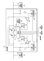
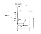
- FIG. 1 is a block diagram showing a main configuration of the power supply system according to the first embodiment.
- the power supply system 1 is suitably mounted on a vehicle and includes a prevention device 10, a first capacitor 11, a first load 12, a starter 13, a generator 14, a second load 15, and a second capacitor 16.
- One end of the prevention device 10 is connected to the positive electrode of the first capacitor 11 and one end of each of the first load 12 and the starter 13.
- the other end of the prevention device 10 is connected to one end of each of the generator 14 and the second load 15 and the positive electrode of the second battery 16.
- the negative electrodes of the first capacitor 11 and the second capacitor 16 and the other ends of the first load 12, the starter 13, the generator 14, and the second load 15 are grounded.
- the generator 14 generates AC regenerative power when, for example, the brake pedal of the vehicle is depressed and the vehicle speed is decelerated.
- the generator 14 rectifies the generated AC regenerative power into DC regenerative power.
- the generator 14 supplies the rectified DC regenerative power to the first capacitor 11 and the first load 12 via the prevention device 10 and also to the second load 15 and the second capacitor 16.
- the second load 15 is an electric device mounted on the vehicle, and is supplied with power from the first capacitor 11, the generator 14, and the second capacitor 16.
- the second battery 16 is an electric double layer capacitor, a lithium ion battery, or the like, and stores the electric power supplied from the generator 14.
- the second battery 16 is further fed with power from the first battery 11 via the prevention device 10 and stores the power supplied from the first battery 11.
- the second battery 16 supplies the stored power to the first battery 11 and the first load 12 via the prevention device 10 and also to the second load 15.
- the first battery 11 is, for example, a lead storage battery, and is supplied with power from the generator 14 and the second battery 16 via the prevention device 10, and stores the power supplied from the generator 14 and the second battery 16.
- the first capacitor 11 supplies the stored power to the first load 12 and the starter 13 and also supplies the second load 15 and the second capacitor 16 via the prevention device 10.
- the first load 12 is an electric device mounted on the vehicle, similar to the second load 15, and is supplied with power from the first capacitor 11, the generator 14, and the second capacitor 16.
- the starter 13 is a motor for starting an engine (not shown), and operates using the electric power stored in the first capacitor 11.
- the prevention device 10 has a prior signal that notifies in advance that the starter 13 is activated, a first activation signal that notifies in advance that the first load 12 is activated, and that the second load 15 is activated in advance. And a second operation signal to be notified.
- the prevention device 10 interrupts energization when a current equal to or greater than the cutoff threshold flows between both ends of the device, and prevents an overcurrent from flowing in the current path of the current flowing between both ends of the device.
- the prevention device 10 also cuts off the power supply when a prior signal is input. As a result, the starter 13 is fed by the first battery 11.
- the prevention apparatus 10 adjusts a cutoff threshold, when a 1st operation signal or a 2nd operation signal is input.
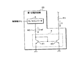
- FIG. 2 is a block diagram showing a main configuration of the prevention device 10.
- the prevention device 10 includes N-channel FETs 21 and 22, a control unit 23, a temperature detection unit 24, a first constant current circuit 25, a first comparator 26, a first timer 27, a second constant current circuit 28, and a second comparator 29.
- the diodes D1 and D2 are parasitic diodes of the FETs 21 and 22, respectively.
- the drain of the FET 21 and the cathode of the diode D1 are connected to one end of each of the generator 14 and the second load 15 and the positive electrode of the second capacitor 16.
- the anodes of the diodes D1 and D2 and the source of the FET 22 are connected to the source of the FET 21.
- the drain of the FET 22 is connected to the cathode of the diode D2, the positive electrode of the first capacitor 11, and one end of each of the first load 12 and the starter 13.
- the gates of the FETs 21 and 22 are connected to the control unit 23, and the control unit 23 is further connected to the temperature detection unit 24.
- the control unit 23 is also grounded.
- Each of the first load 12 and the second load 15 functions as a load in the claims.
- One end of the resistor R1 is connected to the drain of the FET 21, and the other end of the resistor R1 is connected to the first constant current circuit 25 and the negative terminal of the first comparator 26.
- the first constant current circuit 25 is further connected to the control unit 23 and is also grounded.
- the positive terminal of the first comparator 26 is connected to the drain of the FET 22, and the output terminal of the first comparator 26 is connected to the control unit 23.
- the first timer 27 is also connected to the control unit 23.
- One end of the resistor R2 is connected to the drain of the FET 22, and the other end of the resistor R2 is connected to the second constant current circuit 28 and the negative terminal of the second comparator 29.
- the second constant current circuit 28 is further connected to the control unit 23 and is also grounded.
- the positive terminal of the second comparator 29 is connected to the drain of the FET 21, and the output terminal of the second comparator 29 is connected to the control unit 23.
- FET21 and 22 each function as a switch. For each of the FETs 21 and 22, when a voltage higher than a certain voltage is applied to the gate by the control unit 23, a current can flow between the drain and the source, and each of the FETs 21 and 22 is turned on. Further, when the voltage applied to the gate by the control unit 23 is less than a certain voltage for each of the FETs 21 and 22, no current flows between the drain and the source, and the FETs 21 and 22 are turned off. The controller 23 simultaneously turns on / off the FETs 21 and 22 by adjusting the voltage applied to the gates of the FETs 21 and 22.
- the switch in the claims corresponds to the entire two FETs 21 and 22.
- the source of the FET 21 is connected to the source of the FET 22, the anode of the diode D1 is connected to the anode of the diode D2. Therefore, when each of the FETs 21 and 22 is off, no current flows through the diodes D1 and D2.
- the FETs 21 and 22 are provided in a current path of a current flowing between both ends of the prevention device 10.
- the first constant current circuit 25 allows a constant current to flow from the FET 21 side of the resistor R1 toward the other side.
- the value I1 of the current flowing through the first constant current circuit 25 is changed by the control unit 23.
- the control unit 23 functions as changing means in the claims.
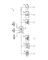
- FIG. 3 is a circuit diagram of the first constant current circuit 25.
- the first constant current circuit 25 includes a current mirror circuit 4 and resistors R3, R4, and R5.
- the current mirror circuit 4 has two NPN bipolar transistors 40 and 41. Each of the bipolar transistors 40 and 41 has a base, an emitter, and a collector. The other end of the resistor R1 is connected to the collector of the bipolar transistor 40 of the current mirror circuit 4.
- the base of the bipolar transistor 40 is connected to the base and collector of the bipolar transistor 41.
- the emitters of the bipolar transistors 40 and 41 are grounded, and the potentials at the emitters of the bipolar transistors 40 and 41 are substantially the same.
- the collector of the bipolar transistor 41 is connected to one end of the resistor R3, and the other end of the resistor R3 is connected to one end of each of the resistors R4 and R5.
- the other end of the resistor R4 is connected to the control unit 23, and a predetermined voltage Vcc is applied to the other end of the resistor R5.
- each of the bipolar transistors 40 and 41 a current having a large / small value flows between the emitter and the collector in accordance with the high / low voltage between the base and the emitter.
- the value of the current flowing between the collector and emitter of the bipolar transistor 40 is multiplied by a predetermined number between the collector and emitter of the bipolar transistor 40.
- the specified current flows.
- Each of the bipolar transistors 40 and 41 functions as the other and one transistor in the claims.
- the base, emitter and collector of each of the bipolar transistors 40 and 41 correspond to a first end, a second end and a third end in the claims.
- the voltage Vcc is applied between the other end of the resistor R5 and the emitter of the bipolar transistor 41.
- a current flows from the other end of the resistor R5 in the order of the resistor R3 and the collector and emitter of the bipolar transistor 41. Since the same voltage is applied to the bases of the bipolar transistors 40 and 41, a current having a value I1 obtained by multiplying the current value Iref flowing between the collector and emitter of the bipolar transistor 41 by a predetermined number flows through the resistor R1.
- the voltage Vcc is generated by a regulator (not shown), for example.
- the regulator generates a voltage Vcc from the output voltage of the second battery 16.
- the controller 23 changes the current value Iref by either adjusting the potential at the other end of the resistor R4 or opening the other end of the resistor R4. As a result, the current value I1 is changed. Specifically, the control unit 23 applies the voltage Vcc with reference to the potential of the emitter of the bipolar transistor 41 to the other end of the resistor R4, or grounds one end of the resistor R4 so that the other end of the resistor R4 is grounded. Adjust the potential at the edges.
- FIG. 4 is an equivalent circuit diagram of the first constant current circuit 25 in each output state of the control unit 23.
- the output state that the control unit 23 outputs to the other end of the resistor R4 includes a state where the voltage Vcc is applied to one end of the resistor R4, a state where one end of the resistor R4 is opened, and one end of the resistor R4 is grounded.
- resistors R3 and R5 are connected in series.
- the combined resistance value of the resistors R4 and R5 connected in parallel is smaller than the resistance value of the resistor R5. Therefore, the current value Iref when the control unit 23 opens the other end of the resistor R4 is smaller than the current value Iref when the control unit 23 applies the voltage Vcc to the other end of the resistor R4.
- the controller 23 adjusts the potential at the other end of the resistor R4 and opens the other end of the resistor R4, whereby the current value I1 that the first constant current circuit 25 passes through the resistor R1, That is, the value of the current flowing between the emitter and collector of the bipolar transistor 40 can be easily changed.
- the potential at the other end of the resistor R4 may be adjusted to a potential other than these in addition to the potential at the other end of the resistor R5 to which the voltage Vcc is applied and the ground potential. In this case, the current value Iref can be adjusted more finely.
- the first comparator 26 compares the potential at the drain of the FET 22 with the potential at the other end of the resistor R1.
- the first comparator 26 outputs a high level voltage from the output terminal to the control unit 23 when the potential at the drain of the FET 22 is higher than the potential at the other end of the resistor R1. Further, the first comparator 26 outputs a low level voltage from the output terminal to the control unit 23 when the potential at the drain of the FET 22 is lower than the potential at the other end of the resistor R1.
- the first comparator 26 functions as a comparison unit.
- the first timer 27 receives from the control unit 23 a start instruction for instructing the start of timekeeping and an end instruction for instructing the end of timekeeping.
- the first timer 27 starts timing when a start instruction is input from the control unit 23, and the first time measured by the first timer 27 is read by the control unit 23.
- the first timer 27 ends time counting when an end instruction is input from the control unit 23.
- the configuration and operation of the second constant current circuit 28, the second comparator 29, and the second timer 30 are the same as those of the first constant current circuit 25, the first comparator 26, and the first timer 27.
- the resistor R1 the FET 21, and the FET 22 described in the description of the first constant current circuit 25, the first comparator 26, and the first timer 27, respectively.
- the resistor R2 the FET 22 and the FET 21.
- the second constant current circuit 28 flows a constant current from the FET 22 side of the resistor R2 toward the other side, and the current value I2 that the second constant current circuit 28 flows is changed by the control unit 23.
- the second comparator 29 compares the potential at the drain of the FET 21 with the potential at the other end of the resistor R2.
- the controller 23 reads the second time measured by the second timer 30 from the second timer 30. Similar to the first comparator 26, the second comparator 29 functions as a comparison unit. And the control part 23 can change easily the value I2 of the electric current which the 2nd constant current circuit 28 flows into resistance R2.
- the temperature detection unit 24 is configured using, for example, a thermistor, and detects the temperature around the switch (hereinafter referred to as switch temperature). The switch temperature detected by the temperature detection unit 24 is read by the control unit 23.
- the controller 23 receives a pre-signal, a first operation signal, and a second operation signal. Further, a high level voltage or a low level voltage is input to the control unit 23 from the output terminals of the first comparator 26 and the second comparator 29.
- the control unit 23 turns off the FETs 21 and 22 when a prior signal is input. Then, the starter 13 is operated using the electric power of the first battery 11, and the engine is started. The controller 23 turns on the FETs 21 and 22 after a sufficient time has passed for the engine to start after turning off the FETs 21 and 22.
- the control unit 23 normally turns on the FETs 21 and 22 for other periods excluding the period related to the operation of the starter 13. While the FETs 21 and 22 are on, current flows between the drains of the FETs 21 and 22.
- the value of the current flowing between the drains of the FETs 21 and 22 is referred to as a switch current value.
- the control unit 23 turns off the FETs 21 and 22 when the switch current value is equal to or greater than a certain current value, and prevents an overcurrent from flowing between both ends of the prevention device 10.
- the controller 23 determines the value I1 of the current that the first constant current circuit 25 passes through the resistor R1 as described above. Change to Similarly, the control unit 23 changes the value I2 of the current that the second constant current circuit 28 passes through the resistor R2 based on the temperature detected by the temperature detection unit 24 and the second time measured by the second timer 30. To do. Furthermore, the control unit 23 switches the FETs 21 and 22 from on to off in accordance with the voltages output from the first comparator 26 and the second comparator 29.
- the FETs 21 and 22, the control unit 23, the temperature detection unit 24, the first constant current circuit 25, the first comparator 26, and the first timer 27 prevent an overcurrent from flowing from the drain of the FET 21 to the drain of the FET 22.
- the FETs 21 and 22, the control unit 23, the temperature detection unit 24, the second constant current circuit 28, the second comparator 29, and the second timer 30 prevent an overcurrent from flowing from the drain of the FET 22 to the drain of the FET 21.
- the control unit 23 performs a first prevention process to prevent an overcurrent from flowing from the drain of the FET 21 to the drain of the FET 22, and a second prevention process to prevent an overcurrent from flowing from the drain of the FET 22 to the drain of the FET 21. Execute the process.
- the control unit 23 executes the first prevention process and the second prevention process when the FETs 21 and 22 are turned on.
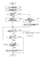
- FIG. 5 is a flowchart showing the first prevention process executed by the control unit 23.
- the control unit 23 reads the switch temperature detected by the temperature detection unit 24 from the temperature detection unit 24 (step S1), and sets the first current value to small / large according to the high / low of the read switch temperature. Set (step S2).
- the control part 23 determines whether the 1st load 12 will operate
- the control unit 23 determines that the first load 12 will be operated when the first operation signal is input, and the first load 12 is operating or stopped when the first operation signal is not input. It is determined that the first load 12 will not operate from now on.
- the control unit 23 also functions as a determination unit in the claims.
- the control unit 23 changes the current value I1 to the first current value set in step S2 (step S4).
- the controller 23 changes the current value I1 to a value obtained by adding a predetermined current value ⁇ I to the first current value set in step S2 (step S2).
- S5 The time measurement by the first timer 27 is started by outputting a start instruction to the first timer 27 (step S6).
- the control unit 23 increases the current value I1 from the first current value by the current value ⁇ I.
- the control unit 23 sets the first current value to small / large according to the switch temperature high / low, and sets the current value I1 to the first current value or the first current value.
- the current value is changed by adding ⁇ I. In other words, the control unit 23 changes the current value I1 to small / large according to the switch temperature high / low.
- Step S4 or Step S6 the control unit 23 determines whether or not the conduction between the drains of the FETs 21 and 22 should be cut off based on the voltage output from the first comparator 26 (Step S7). ).
- the potential at the drain of the FET 21 is Vb1
- the resistance value of the resistor R1 is r1
- the sum of the on-resistance values of the FETs 21 and 22 is rs
- the absolute value of the switch current value is Is.
- the value obtained by subtracting the potential at the other end of the resistor R1 from the potential at the drain of the FET 22 is (r1 ⁇ I1 ⁇ rs ⁇ Is).
- the first comparator 26 outputs a high level voltage from the output terminal to the control unit 23.
- the control unit 23 determines in step S7 that energization should not be interrupted.
- the first comparator 26 When the absolute value Is of the switch current value exceeds (r1 ⁇ I1 / rs), the first comparator 26 outputs a low level voltage to the control unit 23 from the output terminal. When the first comparator 26 outputs a low level voltage, the control unit 23 determines in step S7 that energization should be interrupted.
- the potential at the drain of the FET 22 is Vb2.
- the potential at the other end of the resistor R1 is (Vb2-rs ⁇ Is-r1 ⁇ I1).
- the value obtained by subtracting the potential at the other end of the resistor R1 from the potential Vb2 at the drain of the FET 22 is (rs ⁇ Is + r1 ⁇ I1), and always exceeds zero. Therefore, when current flows from the drain of the FET 22 to the drain of the FET 21, the first comparator 26 always outputs a high level voltage from the output terminal, and the control unit 23 should not cut off the energization in step S7. judge.
- the control unit 23 determines whether or not the first timer 27 is timing (step S8). When it is determined that the first timer 27 is measuring time (S8: YES), the control unit 23 determines whether the first time measured by the first timer 27 is equal to or longer than a preset set time. It is determined whether or not (step S9).
- the control unit 23 When it is determined that the first measured time is less than the set time (S9: NO), the control unit 23 returns the process to step S7, and the current value I1 is changed to the first time until the first measured time becomes equal to or greater than the set time. In a state where the current value is changed to the current value obtained by adding the current value ⁇ I to one current value, the determination as to whether or not to cut off energization is repeated.
- the control unit 23 When it is determined that the first measured time is equal to or longer than the set time (S9: YES), the control unit 23 outputs an end display to the first timer 27, thereby ending the time measurement by the first timer 27 (step S10). ). When it is determined that the first timer 27 has not timed (S8: NO), or after executing Step S10, the control unit 23 ends the first prevention process.
- the control unit 23 repeats the first prevention process while the FETs 21 and 22 are turned on.
- the first load 12 is in operation when the control unit 23 executes the first prevention process.
- the control unit 23 returns the current value I1 to the current value before the increase in step S5, that is, the first current value.
- control unit 23 determines that the energization should be interrupted (S7: YES), that is, the comparison result performed by the first comparator 26 indicates that the potential at the drain of the FET 22 is lower than the potential at the other end of the resistor R1. Is turned off, the FETs 21 and 22 are turned off (step S11). Thereafter, the control unit 23 ends the first prevention process.
- the second prevention process for preventing the overcurrent from flowing from the drain of the FET 22 to the drain of the FET 21 is the same as the first prevention process.
- the first load 12 the first constant current circuit 25, the first comparator 26, the first timer 27, the first current value, the current value I1, and the first operation signal in the description of the first prevention process.
- the first clock time correspond to the second load 15, the second constant current circuit 28, the second comparator 29, the second timer 30, the second current value, the current value I2, the second operation signal, and the second clock time, respectively. To do.
- the second current value is a current value set in a step corresponding to step S2 of the first prevention process in the second prevention process, and the switch temperature read from the temperature detection unit 24 is the same as the first current value. It is set to small / large according to the high / low of.
- the resistance value of the resistor R2 is r2.
- the potential at the drain of the FET 21 is (Vb2-rs ⁇ Is), and the other end of the resistor R2, that is, the second constant current circuit 28 side of the resistor R2
- the potential at one end is (Vb2-r2 ⁇ I2).
- the value obtained by subtracting the potential at the other end of the resistor R2 from the potential at the drain of the FET 22 is (r2 ⁇ I2 ⁇ rs ⁇ Is).
- the second comparator 29 outputs a high level voltage from the output terminal to the control unit 23.
- the control unit 23 It is determined that energization should not be interrupted.
- the second comparator 29 outputs a low level voltage from the output terminal, and in the second prevention process, the control unit 23 cuts off the energization. Determine that it should be.
- the potential at the other end of the resistor R2 is (Vb1 ⁇ rs ⁇ Is ⁇ r2 ⁇ I2). Since the potential at the drain of the FET 21 is Vb1, the value obtained by subtracting the potential at the other end of the resistor R2 from the potential at the drain of the FET 21 is (rs ⁇ Is + r2 ⁇ I2), which always exceeds zero. Therefore, when the current flows from the drain of the FET 21 to the drain of the FET 22, the second comparator 29 always outputs a high level voltage from the output terminal, and in the second prevention process, the control unit 23 should cut off the energization. It is determined that it is not.
- the control unit 23 repeats the first prevention process and the second prevention process until the FETs 21 and 22 are turned off in either the first prevention process or the second prevention process. At this time, the control unit 23 may be configured to alternately execute the first prevention process and the second prevention process, or may be configured to execute the first prevention process and the second prevention process in parallel. Also good.
- the first comparator 26 changes the threshold potential to be compared with the potential at the drain of the FET 22, that is, the potential at the other end of the resistor R1. Can do. Further, by changing the current value I2, the threshold potential that the second comparator 29 compares with the potential at the drain of the FET 21, that is, the potential at the other end of the resistor R2 can be changed.
- the on-resistance values of the FETs 21 and 22 vary.
- the manufacturing FETs 21 and 22 are turned off at an appropriate timing, and the energization is performed. Is cut off.
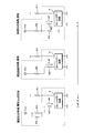
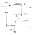
- FIG. 6 is an explanatory view showing the effect of the prevention device 10.
- a graph showing the relationship between the allowable current value, which is the absolute value of the allowable switch current value, and the switch temperature is drawn with a thin line.
- a graph showing the relationship between the cutoff threshold value, which is the absolute value of the switch current value at which the energization is cut off, and the switch temperature is drawn with a bold line.
- the allowable current value decreases as the switch temperature increases. This is because, when the switch temperature is high, even when the switch current value Is is relatively small, for example, the structures of the FETs 21 and 22 may change, and the FETs 21 and 22 may lose their functions as switches. Because there is.
- the first current value and the second current value are set to small / large according to the high / low of the switch temperature, so that the current values I1, I2 Each becomes smaller as the switch temperature is higher.
- the cutoff threshold value represented by (r1 ⁇ I1 / rs) in the first process and represented by (r2 ⁇ I2 / rs) in the second process is smaller as the switch temperature is higher. Therefore, as indicated by the thick line in FIG. 6, the cutoff threshold can be set to a value less than the allowable current value at each switch temperature. For this reason, failure of the FETs 21 and 22 can be surely prevented, and current can efficiently flow between the drains of the FETs 21 and 22.
- FIG. 7 is an explanatory view showing another effect of the prevention device 10.
- FIG. 7 shows an example of the transition of the current value I1, the absolute value Is of the switch current value, and the cutoff threshold.
- the switch temperature is assumed to be constant.
- the control unit 23 changes the current value I1 to a value obtained by adding the current value ⁇ I to the first current value.
- the threshold potential to be compared with the potential at the drain of the FET 22, that is, the potential at the other end of the resistor R1 is lowered, and the cutoff threshold value expressed by (r1 ⁇ I1 / rs) is increased.
- the current value I1 is returned to the first current value after the design time has elapsed. .
- the cutoff threshold value also returns to the value when the current value I1 is the first current value.
- the set time is preferably longer than the time from when the first operation signal is input to the control unit 23 until the inrush current is generated and the absolute value Is of the switch current value is stabilized.
- the effect obtained by the control unit 23 executing the first prevention process is described with reference to FIG. 7, but the same effect can be obtained when the control unit 23 executes the second prevention process. That is, when the second load 15 is to be operated, the control unit 23 raises the current value I2 to a value obtained by adding the current value ⁇ I to the second current value. The probability of turning off each one is low. Further, when the set time has elapsed since the current value I2 was raised, the current value I2 is returned to the second current value. Therefore, the threshold potential to be compared with the potential at the drain of the FET 21 is set only during the period when the inrush current flows. It can be raised to increase the blocking threshold.
- FIG. 8 is a circuit diagram of the first constant current circuit 25 in the second embodiment.
- the second embodiment is different from the first embodiment in the circuit configurations of the first constant current circuit 25 and the second constant current circuit 28.
- the differences between the second embodiment and the first embodiment will be described. Since the other configuration except the configuration to be described later is the same as that of the first embodiment, the same reference numerals are given and the description thereof is omitted.
- the first constant current circuit 25 in the second embodiment includes a current mirror circuit 4 and resistors R3, R4, and R5, which are connected in the same manner as in the first embodiment.
- the first constant current circuit 25 according to the second embodiment further includes a resistor R6. One end of the resistor R6 is connected to one end of the resistor R5, and the other end of the resistor R6 is connected to the control unit 23.
- the control unit 23 performs the same operation on the other end of the resistor R6 as the operation performed on the other end of the resistor R4. That is, the control unit 23 adjusts the potential at the other end of the resistor R6 and opens the other end of the resistor R6.
- the current value Iref when the voltage Vcc is applied to the other end of the resistor R6 is the largest. Then, the current value Iref when the other end of the resistor R6 is opened is the next largest, and the current value Iref when the other end of the resistor R6 is grounded is the smallest.
- the addition of the resistor R6 allows the control unit 23 to control the current value Iref more finely.
- the number of values of the current value Iref is nine, and the control unit 23 can change the current value I1 to nine values.
- the potential at the other end of each of the resistors R4 and R6 may be adjusted to a potential other than these in addition to the potential at the other end of the resistor R5 to which the voltage Vcc is applied and the ground potential. In this case, the current value Iref can be adjusted more finely.
- the control unit 23 can control the current value I2 more finely.
- the control unit 23 in the second embodiment performs the first prevention process and the second prevention process similarly to the first embodiment, and only the configuration for changing the current values I1 and I2 is different from that in the first embodiment.
- the prevention device 10 in No. 2 has the same effect as that of the first embodiment.
- the number of resistors for adjusting the current value Iref is not limited to two, and may be three or more.
- the third and subsequent resistors are connected in the same manner as the resistor R4 or the resistor R6, and the controller 23 performs the same operation as that performed at the other end of the resistor R4.
- FIG. 9 is a circuit diagram of the first constant current circuit 25 in the third embodiment.
- the third embodiment is different from the first embodiment in the circuit configurations of the first constant current circuit 25 and the second constant current circuit 28.
- the differences between the third embodiment and the first embodiment will be described. Since the other configuration except the configuration to be described later is the same as that of the first embodiment, the same reference numerals are given and the description thereof is omitted.
- the first constant current circuit 25 in the third embodiment has a current mirror circuit 4 and a resistor R3, which are connected in the same manner as in the first embodiment.
- the first constant current circuit 25 in the third embodiment further includes a D / A converter 5.
- the D / A converter 5 is connected to the other end of the resistor R3 and the control unit 23.
- One end of the resistor R3 is connected to the collector and base of the bipolar transistor 41.
- a digital signal indicating the height of the voltage to be applied between the other end of the resistor R 3 and the emitter of the bipolar transistor 41 is input to the D / A converter 5 from the control unit 23.
- the D / A converter 5 applies a voltage having a height indicated by the digital signal input from the control unit 23 between the other end of the resistor R 3 and the emitter of the bipolar transistor 41. Thereby, a current flows in the order of the other end of the resistor R3 and the collector and emitter of the bipolar transistor 41.
- the current value Iref (Vda ⁇ Vbe) / r3 (1)
- r3 is a resistance value of the resistor R3
- Vbe is a voltage between the base and the emitter of the bipolar transistor 41.
- the current value Iref becomes large / small according to the high / low of the voltage Vda.
- the control unit 23 adjusts the height of the voltage Vda by outputting a digital signal indicating various heights to the D / A converter 5. As a result, the control unit 23 changes the current value Iref and changes the current value I1. In the first constant current circuit 25 configured as described above, the control unit 25 can change the current value I1 with a simple configuration.
- the control unit 23 can change the current value I2 with a simple configuration. .
- the control unit 23 in the third embodiment performs the first prevention process and the second prevention process similarly to the first embodiment, and only the configuration for changing the current values I1 and I2 is different from the first embodiment.
- the prevention device 10 according to the third embodiment has the same effect as the first embodiment.
- the current value I1 increases from the first current value (or second current value) when the first load 12 (or second load 15) is to operate from now on. Then, the timing for returning to the first current value (or the second current value) is not limited after the set time has elapsed since the current value I1 (or the current value I2) is increased. For example, the absolute value Is of the switch current value is monitored, and when the absolute value Is of the switch current value is stabilized, the current value I1 (or current value I2) is changed to the first current value (or second current value). You may return.
- the current value I1 (or the current value I2) is changed, and the current value I1 (or the current value I2) is changed according to the switch temperature. Both of the processes to be changed need not be performed, and either one may be performed. Further, the condition for changing the current value I1 (or the current value I2) is not limited to the case where the first load 12 (or the second load 15) is to be operated or the switch temperature is changed. It may be a case where an instruction to change the current value I1 (or current value I2) is received from a person.
- the drain of the FET 21 is connected to the drain of the FET 22, the source of the FET 21 is connected to one end of the resistor R1 and the plus terminal of the second comparator 29, and the source of the FET 22 is connected to one end of the resistor R2. 1 may be connected to the plus terminal of the comparator 26.
- the cathodes of the diodes D1 and D2 are connected to the sources of the FETs 21 and 22, and the anodes are connected to the drains of the FETs 21 and 22, respectively. For this reason, since the cathode of the diode D1 is connected to the cathode of the diode D2, no current flows through the diodes D1 and D2 when the FETs 21 and 22 are off.
- each of the FETs 21 and 22 may be a P-channel FET or a bipolar transistor.
- One semiconductor switch may be used instead of the FETs 21 and 22.
- This semiconductor switch is preferably a switch in which no current flows between both ends of the semiconductor switch while it is off.
- the first constant current circuit 25 and the second constant current circuit 28 are not limited to the configuration using bipolar transistors, and may be configured using FETs. For example, when two N-channel FETs are used instead of the bipolar transistors 40 and 41, the gates, sources and drains of the two FETs correspond to the bases, emitters and collectors of the bipolar transistors 40 and 41, respectively. Furthermore, the configurations of the first constant current circuit 25 and the second constant current circuit 28 may be different.
Landscapes
- Emergency Protection Circuit Devices (AREA)
- Electronic Switches (AREA)
- Protection Of Static Devices (AREA)
Priority Applications (3)
| Application Number | Priority Date | Filing Date | Title |
|---|---|---|---|
| EP15758498.8A EP3116129B1 (en) | 2014-03-05 | 2015-02-20 | Preventive apparatus |
| CN201580011624.6A CN106063129B (zh) | 2014-03-05 | 2015-02-20 | 防止装置 |
| US15/123,751 US10135234B2 (en) | 2014-03-05 | 2015-02-20 | Preventive apparatus |
Applications Claiming Priority (2)
| Application Number | Priority Date | Filing Date | Title |
|---|---|---|---|
| JP2014043038A JP6311357B2 (ja) | 2014-03-05 | 2014-03-05 | 防止装置 |
| JP2014-043038 | 2014-03-05 |
Publications (1)
| Publication Number | Publication Date |
|---|---|
| WO2015133294A1 true WO2015133294A1 (ja) | 2015-09-11 |
Family
ID=54055104
Family Applications (1)
| Application Number | Title | Priority Date | Filing Date |
|---|---|---|---|
| PCT/JP2015/054736 Ceased WO2015133294A1 (ja) | 2014-03-05 | 2015-02-20 | 防止装置 |
Country Status (5)
| Country | Link |
|---|---|
| US (1) | US10135234B2 (enExample) |
| EP (1) | EP3116129B1 (enExample) |
| JP (1) | JP6311357B2 (enExample) |
| CN (1) | CN106063129B (enExample) |
| WO (1) | WO2015133294A1 (enExample) |
Families Citing this family (6)
| Publication number | Priority date | Publication date | Assignee | Title |
|---|---|---|---|---|
| JP2017069716A (ja) * | 2015-09-29 | 2017-04-06 | 株式会社オートネットワーク技術研究所 | 半導体装置及び制御装置 |
| JP6610446B2 (ja) * | 2016-06-21 | 2019-11-27 | 株式会社オートネットワーク技術研究所 | 給電制御装置 |
| JP6426783B2 (ja) * | 2017-03-14 | 2018-11-21 | ファナック株式会社 | パワー素子の異常検知機能を備えたモータ駆動装置 |
| JP6907984B2 (ja) * | 2018-03-23 | 2021-07-21 | 株式会社オートネットワーク技術研究所 | 制御装置、制御方法及びコンピュータプログラム |
| US11495836B2 (en) * | 2019-11-11 | 2022-11-08 | Samsung Sdi Co., Ltd. | Control unit for a battery system |
| JP7472577B2 (ja) * | 2020-03-23 | 2024-04-23 | 株式会社オートネットワーク技術研究所 | 電流制御装置、スイッチ制御装置、電流制御方法及びコンピュータプログラム |
Citations (3)
| Publication number | Priority date | Publication date | Assignee | Title |
|---|---|---|---|---|
| JPH03101129U (enExample) * | 1990-01-30 | 1991-10-22 | ||
| JP2007134780A (ja) * | 2005-11-08 | 2007-05-31 | Yazaki Corp | 自己診断機能を備えた負荷駆動装置 |
| JP2013205173A (ja) * | 2012-03-28 | 2013-10-07 | Lapis Semiconductor Co Ltd | 半導体装置及び電池監視システム |
Family Cites Families (12)
| Publication number | Priority date | Publication date | Assignee | Title |
|---|---|---|---|---|
| US5864458A (en) * | 1995-09-14 | 1999-01-26 | Raychem Corporation | Overcurrent protection circuits comprising combinations of PTC devices and switches |
| JP3403309B2 (ja) * | 1997-01-31 | 2003-05-06 | 株式会社ケンウッド | 充電装置 |
| JP3589392B2 (ja) | 1999-02-26 | 2004-11-17 | 矢崎総業株式会社 | 過電流検出回路及び過電流検出・保護回路 |
| JP2001161025A (ja) * | 1999-11-30 | 2001-06-12 | Ando Electric Co Ltd | 電流制限装置 |
| JP2002017036A (ja) * | 2000-06-29 | 2002-01-18 | Nissan Motor Co Ltd | 過電流検知回路 |
| JP3914004B2 (ja) * | 2001-05-25 | 2007-05-16 | 矢崎総業株式会社 | 半導体素子の過電流検出・保護装置 |
| JP2003101129A (ja) | 2001-07-18 | 2003-04-04 | Tdk Corp | レーザダイオード駆動回路および駆動方法、並びにそれを用いた光ヘッド |
| US6917503B2 (en) * | 2003-10-29 | 2005-07-12 | Texas Instruments Incorporated | Programmable current limiting using a shunt resistor |
| JP4808047B2 (ja) * | 2006-03-03 | 2011-11-02 | 新日本無線株式会社 | 電流源回路 |
| US7839097B2 (en) * | 2007-02-03 | 2010-11-23 | Kinetic Technologies | System and method for wide-range high-accuracy-low-dropout current regulation |
| JP5171402B2 (ja) * | 2008-06-04 | 2013-03-27 | 矢崎総業株式会社 | 負荷回路の過電流保護装置 |
| TWI515987B (zh) | 2011-07-22 | 2016-01-01 | 鴻海精密工業股份有限公司 | 過壓過流保護電路 |
-
2014
- 2014-03-05 JP JP2014043038A patent/JP6311357B2/ja not_active Expired - Fee Related
-
2015
- 2015-02-20 US US15/123,751 patent/US10135234B2/en active Active
- 2015-02-20 CN CN201580011624.6A patent/CN106063129B/zh not_active Expired - Fee Related
- 2015-02-20 WO PCT/JP2015/054736 patent/WO2015133294A1/ja not_active Ceased
- 2015-02-20 EP EP15758498.8A patent/EP3116129B1/en active Active
Patent Citations (3)
| Publication number | Priority date | Publication date | Assignee | Title |
|---|---|---|---|---|
| JPH03101129U (enExample) * | 1990-01-30 | 1991-10-22 | ||
| JP2007134780A (ja) * | 2005-11-08 | 2007-05-31 | Yazaki Corp | 自己診断機能を備えた負荷駆動装置 |
| JP2013205173A (ja) * | 2012-03-28 | 2013-10-07 | Lapis Semiconductor Co Ltd | 半導体装置及び電池監視システム |
Non-Patent Citations (1)
| Title |
|---|
| See also references of EP3116129A4 * |
Also Published As
| Publication number | Publication date |
|---|---|
| EP3116129A4 (en) | 2017-03-15 |
| US20170018918A1 (en) | 2017-01-19 |
| CN106063129A (zh) | 2016-10-26 |
| JP2015170918A (ja) | 2015-09-28 |
| US10135234B2 (en) | 2018-11-20 |
| EP3116129A1 (en) | 2017-01-11 |
| CN106063129B (zh) | 2019-03-22 |
| JP6311357B2 (ja) | 2018-04-18 |
| EP3116129B1 (en) | 2022-06-08 |
Similar Documents
| Publication | Publication Date | Title |
|---|---|---|
| JP6311357B2 (ja) | 防止装置 | |
| US9825555B2 (en) | Semiconductor control device, switching device, inverter, and control system | |
| JP6624339B2 (ja) | 電源装置 | |
| CN107276137A (zh) | 充电装置 | |
| US20180304827A1 (en) | Current control device, current control method, and computer program | |
| US11004626B2 (en) | Power supply control device, power supply control method, and computer program | |
| JP2017118791A (ja) | 給電制御装置 | |
| JP2015100240A (ja) | 保護装置及び変圧システム | |
| CN111095722A (zh) | 电池单元及电池单元的控制方法 | |
| JP2017229154A (ja) | バッテリ装置 | |
| JP2017188983A (ja) | 電源供給装置 | |
| US20250093417A1 (en) | Electronic control device and electronic control method | |
| US20190165561A1 (en) | Power supply control apparatus, power supply control method, and computer program | |
| EP3048713B1 (en) | Power supply apparatus | |
| CN111799759A (zh) | 车载ecu输出电源的过流保护电路及其控制方法 | |
| US10547194B2 (en) | Power supply control apparatus | |
| JP2019198171A (ja) | 電力供給装置 | |
| JP5048458B2 (ja) | バッテリ充電器 | |
| JP2015035924A (ja) | 過電流保護装置 | |
| WO2018147102A1 (ja) | スイッチ制御装置 | |
| KR102246702B1 (ko) | 전동식 조향장치의 전자제어장치 및 그 전원제어방법 | |
| CN117280557A (zh) | 电力供给装置 | |
| US9682650B2 (en) | Direction indicator system and direction indicator device for a vehicle | |
| WO2023073754A1 (ja) | 電源遮断装置、モータ駆動装置、および電動パワーステアリング装置 | |
| JP2021029091A (ja) | スイッチング素子の過電流検出装置 |
Legal Events
| Date | Code | Title | Description |
|---|---|---|---|
| 121 | Ep: the epo has been informed by wipo that ep was designated in this application |
Ref document number: 15758498 Country of ref document: EP Kind code of ref document: A1 |
|
| REEP | Request for entry into the european phase |
Ref document number: 2015758498 Country of ref document: EP |
|
| WWE | Wipo information: entry into national phase |
Ref document number: 2015758498 Country of ref document: EP |
|
| NENP | Non-entry into the national phase |
Ref country code: DE |
|
| WWE | Wipo information: entry into national phase |
Ref document number: 15123751 Country of ref document: US |