WO2015119066A1 - 半導体発光素子 - Google Patents
半導体発光素子 Download PDFInfo
- Publication number
- WO2015119066A1 WO2015119066A1 PCT/JP2015/052791 JP2015052791W WO2015119066A1 WO 2015119066 A1 WO2015119066 A1 WO 2015119066A1 JP 2015052791 W JP2015052791 W JP 2015052791W WO 2015119066 A1 WO2015119066 A1 WO 2015119066A1
- Authority
- WO
- WIPO (PCT)
- Prior art keywords
- layer
- light emitting
- semiconductor light
- emitting device
- type semiconductor
- Prior art date
- Legal status (The legal status is an assumption and is not a legal conclusion. Google has not performed a legal analysis and makes no representation as to the accuracy of the status listed.)
- Ceased
Links
Images


Classifications
-
- H—ELECTRICITY
- H10—SEMICONDUCTOR DEVICES; ELECTRIC SOLID-STATE DEVICES NOT OTHERWISE PROVIDED FOR
- H10H—INORGANIC LIGHT-EMITTING SEMICONDUCTOR DEVICES HAVING POTENTIAL BARRIERS
- H10H20/00—Individual inorganic light-emitting semiconductor devices having potential barriers, e.g. light-emitting diodes [LED]
- H10H20/80—Constructional details
- H10H20/81—Bodies
- H10H20/811—Bodies having quantum effect structures or superlattices, e.g. tunnel junctions
-
- H—ELECTRICITY
- H10—SEMICONDUCTOR DEVICES; ELECTRIC SOLID-STATE DEVICES NOT OTHERWISE PROVIDED FOR
- H10H—INORGANIC LIGHT-EMITTING SEMICONDUCTOR DEVICES HAVING POTENTIAL BARRIERS
- H10H20/00—Individual inorganic light-emitting semiconductor devices having potential barriers, e.g. light-emitting diodes [LED]
- H10H20/80—Constructional details
- H10H20/81—Bodies
- H10H20/822—Materials of the light-emitting regions
- H10H20/824—Materials of the light-emitting regions comprising only Group III-V materials, e.g. GaP
- H10H20/825—Materials of the light-emitting regions comprising only Group III-V materials, e.g. GaP containing nitrogen, e.g. GaN
Definitions
- the present invention relates to a semiconductor light emitting device, and more particularly to a semiconductor light emitting device having a peak emission wavelength of 530 nm or more.
- the present invention also relates to a method for manufacturing such a semiconductor light emitting device.
- GaP-based compound semiconductors are mainly used as LEDs having an emission wavelength in the visible light region.
- GaP-based compound semiconductors are indirect transition semiconductors with a band structure, and the transition probability is low, so it is difficult to increase the light emission efficiency. Therefore, development of LEDs in the visible light region using a nitride semiconductor material which is a direct transition type semiconductor is underway.
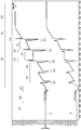
- FIG. 15 is a graph showing the relationship between the peak emission wavelength and the internal quantum efficiency, with the horizontal axis corresponding to the peak emission wavelength and the vertical axis corresponding to the internal quantum efficiency (IQE).
- IQE internal quantum efficiency
- FIG. 15 it can be confirmed that when the peak emission wavelength exceeds 520 nm, the internal quantum efficiency rapidly decreases.
- the wavelength region in which the internal quantum efficiency decreases is called a “green gap region”, and there is a problem that the efficiency decreases in such a wavelength region regardless of the GaP system or the nitride semiconductor system. For this reason, in this green gap region, it is required to increase the internal quantum efficiency and increase the light emission efficiency.
- Nitride semiconductors such as GaN and AlGaN have a wurtzite crystal structure (hexagonal crystal structure).
- the plane of the wurtzite crystal structure is expressed in terms of a crystal plane and orientation using basic vectors represented by a1, a2, a3, and c in a four-index notation (hexagonal crystal index).
- the basic vector c extends in the [0001] direction, and this direction is called “c-axis”.
- a plane perpendicular to the c-axis is called “c-plane” or “(0001) plane”.
- a substrate having a c-plane substrate as a main surface is used as a substrate on which a nitride semiconductor crystal is grown.
- a GaN layer is grown on this substrate at a low temperature, and a nitride semiconductor layer is further grown thereon.
- InGaN which is a mixed crystal of GaN and InN, is used as an active layer constituting a layer that contributes to light emission.
- the lattice constant of GaN is 0.3189 nm
- the lattice constant of InN is 0.354 nm.
- active layers are grown by using a substrate having a nonpolar plane, for example, a (10-10) plane called m-plane perpendicular to the [10-10] direction.
- a substrate having a nonpolar plane for example, a (10-10) plane called m-plane perpendicular to the [10-10] direction.
- m-plane perpendicular to the [10-10] direction for example, see Patent Document 1.
- an object of the present invention is to increase the light emission efficiency of a semiconductor light emitting device having a peak emission wavelength of 530 nm or more formed by growing an active layer in the c-axis direction.
- the present invention is a semiconductor light emitting device having a peak emission wavelength of 530 nm or more, an n-type semiconductor layer; A superlattice layer made of a laminate of a plurality of nitride semiconductors having different band gaps, formed on the n-type semiconductor layer; An active layer formed on the superlattice layer; A p-type semiconductor layer formed on the active layer,
- the active layer is a first layer composed of In X1 Ga 1-X1 N (0 ⁇ X1 ⁇ 0.01) and a first layer composed of In X2 Ga 1-X2 N (0.2 ⁇ X2 ⁇ 1).
- Two layers and a third layer composed of Al Y1 Ga 1-Y1 N (0 ⁇ Y1 ⁇ 1) are laminated, and at least the first layer and the second layer are periodically formed.
- AlGaN AlGaN
- InGaN InGaN
- AlGaN composing the third layer is a mixed crystal of GaN and AlN, and the balance of polarization between Ga having positive charge and Al having negative charge and N having negative charge is broken due to the difference in crystal size and the like, and it is along the c-axis direction.
- An electric field is generated (spontaneous polarization).
- the electric field derived from AlGaN is generated in a direction that cancels the piezoelectric field derived from InGaN.
- the active layer since the active layer has the third layer made of AlGaN, the piezoelectric field generated with respect to the active layer is relieved, and the bending of the band of the active layer can be reduced as compared with the conventional case. As a result, the decrease in the recombination probability of electrons and holes in the active layer is alleviated as compared with the conventional case, and the internal quantum efficiency is improved.
- a superlattice layer made of a laminate of a plurality of nitride semiconductors having different band gaps is provided between the n-type semiconductor layer and the active layer.
- the crystal can be distorted, and the effect of relaxing the lattice strain on the active layer including the second layer composed of InGaN having a high In composition can be obtained.
- an electron block layer (also referred to as an EB layer) is generally provided between an active layer and a p-type semiconductor layer. This prevents the recombination probability from being lowered by electrons injected from the n-type semiconductor layer into the active layer exceeding the active layer and entering the p-type semiconductor layer (also referred to as “overflow”). It is provided for the purpose. In some cases, Si doping is performed on the barrier layer of the active layer in order to increase the efficiency of carrier injection into the active layer, but at this time, the overflow phenomenon appears remarkably.
- n-type semiconductor layer grown before the active layer has a low activation energy, a high activation rate of n-type impurities (such as Si) is realized.
- the p-type semiconductor layer grown after the formation of the active layer containing InGaN needs to be grown at a low temperature in addition to high activation energy. ) Activation rate is reduced. As a result, the n-type impurity concentration becomes higher than the p-type impurity concentration, and the number of electrons overflowing without recombining with holes increases.
- a material with a larger energy band gap than other layers such as an active layer and a p-type semiconductor layer is used as the electron blocking layer, thereby forming a barrier against electrons flowing from the active layer to the p-type semiconductor layer.
- This aims to prevent the electrons injected from the n-type semiconductor layer from overflowing into the p-type semiconductor layer and confine the electrons in the active layer, thereby preventing the recombination probability from being lowered.
- the growth temperature of the active layer has to be lowered in order to increase the In composition.
- the conventional electron block layer is composed of p-AlGaN.
- AlGaN is grown at a low temperature, Al is not sufficiently taken into GaN due to the parasitic reaction between group III and group V, and not only high Al composition AlGaN is formed, but pits are generated due to abnormal growth and the film quality is deteriorated. descend. As a result, the element resistance increases.
- Mg may be doped to make the electron block layer p-type, but if the electron block layer doped with Mg is grown at a low temperature, the activation rate of Mg also decreases. Will rise. Further, the generated pits form a non-light emitting center, and the light output when the same current is supplied is lowered.
- the active layer has the third layer composed of AlGaN.
- the band gap energy of GaN is about 3.4 eV
- the band gap energy of InN is about 0.7 eV
- the band gap energy of AlN is about 6.2 eV. Therefore, in the active layer, the first layer composed of GaN or InGaN with a low In ratio constitutes a barrier layer, and the second layer composed of InGaN with a higher In ratio than the first layer constitutes a light emitting layer
- the third layer made of AlGaN has a higher energy band gap than the first layer, and functions as a layer for realizing a function of preventing the movement of electrons.
- the third layer not only has a function of relaxing the piezoelectric field of InGaN as described above, but also suppresses the overflow of electrons from the n-type semiconductor layer over the active layer into the p-type semiconductor layer. It also has a function. As a result, the reduction in the probability of recombination of electrons and holes due to the overflow of electrons is alleviated without providing an electron blocking layer as in the prior art. Therefore, even if the In composition of the second layer is increased, the InGaN crystal is not broken during the subsequent growth process, and a semiconductor light emitting device having a peak emission wavelength with high emission efficiency of 530 nm or more can be realized.
- the second layer can be formed of In X2 Ga 1-X2 N (0.28 ⁇ X2 ⁇ 0.33) having a thickness of 2.4 nm to 2.8 nm.
- the peak emission wavelength is not less than 530 nm, particularly the peak emission wavelength is not less than 540 nm and not more than 570 nm even when the injected current density is increased to 50 A / cm 2.
- An output light emitting element was realized. Even when the current density to be injected was 25 A / cm 2 , a high-output light emitting element could be realized in the same manner.
- the thickness of the first layer is T1
- the thickness of the second layer is T2
- the thickness of the third layer is T3, 5T2 ⁇ T1 ⁇ 10T2 and T3
- the active layer can be configured to satisfy the relationship ⁇ T2.
- the second layer composed of InGaN with a high In ratio must be grown at a low growth temperature. Since the active layer has a structure in which the first layer, the second layer, and the third layer are laminated, and at least the first layer and the second layer are periodically laminated, the first layer and the third layer are necessarily formed. However, it is necessary to grow at a temperature as low as the growth temperature of the second layer.
- the crystal quality is lowered and the light output is lowered.
- the crystal can grow two-dimensionally to form a good step, and the crystal quality is improved.
- the first layer is too thick, the light output is reduced due to the deterioration of the surface morphology resulting from the low temperature growth. Therefore, a high light output can be realized by setting the film thickness T1 of the first layer to 5T2 ⁇ T1 ⁇ 10T2.
- the third layer having the function of preventing the overflow of electrons has a higher energy band gap than the first layer and the second layer as described above, the p-type is required unless electrons are tunneled in the third layer. It cannot be moved to the semiconductor layer side. For this reason, it is necessary to form the third layer to be thin to some extent. By configuring the third layer to be thinner than the film thickness of the second layer constituting the light emitting layer, electrons can be reliably tunneled in the third layer.
- the film thickness of the second layer can be configured to be 2.4 nm or more and 2.8 nm or less, based on this, the film thickness of the first layer should be 12 nm or more and 28 nm or less. Can do.
- the active layer is formed by periodically forming the first layer, the second layer, and the third layer at a position close to the p-type semiconductor layer, and at a position close to the n-type semiconductor layer.
- the first layer and the second layer may be formed periodically.
- the third layer made of AlGaN has a large band gap energy, and the first layer has a smaller band gap energy than the third layer.
- AlGaN has an electric field due to spontaneous polarization, distortion occurs in the energy band.
- a groove is formed in the band diagram of the valence band of the active layer in the vicinity of the interface between the third layer and the first layer, and holes are two-dimensionally accumulated in this groove (“two-dimensional positive Also called “pore gas”.) Since these holes have high mobility in the two-dimensional direction, there is a possibility that holes injected from the p-type semiconductor layer side into the active layer may cause an overflow phenomenon that exceeds the active layer.
- the holes When a hole overflow phenomenon occurs, the holes accumulate in the InGaN region of the GaN / InGaN superlattice layer formed between the active layer and the n-type semiconductor layer. As a result, electrons injected from the n-type semiconductor layer recombine with holes in the superlattice layer, and light having a wavelength other than the desired wavelength is generated. As a result, light having a peak wavelength different from the peak wavelength of light generated in the active layer is generated, which is not preferable.
- the desired wavelength is 530 nm or more, for example, a high light output cannot be obtained as compared with blue light, so even if light having a different peak wavelength (undesired light) is generated at a low output, it is unfavorable for light of the desired wavelength.
- the output ratio of the desired light will show a high value to some extent.
- the third layer is provided on the p-type semiconductor layer side, the relaxation of the piezoelectric field derived from InGaN and the suppression of the overflow of electrons are realized as described above, and the n-type semiconductor layer side is provided. Since the third layer is not provided, a two-dimensional hole gas with high mobility is not formed, and hole overflow is suppressed.
- a hole barrier layer formed of a nitride semiconductor layer may be provided between the superlattice layer and the active layer. According to this, since the holes overflowing the active layer are suppressed from flowing into the superlattice layer, the generation of undesired light in the GaN / InGaN superlattice layer is suppressed as described above.
- the hole blocking layer can be composed of a nitride semiconductor layer having a Si concentration of 5 ⁇ 10 18 / cm 3 or more and 5 ⁇ 10 19 / cm 3 or less.
- the energy band gap is expanded, and the effect of preventing the movement of holes to the superlattice layer side is enhanced.
- the Si concentration exceeds 5 ⁇ 10 19 / cm 3
- the surface of the nitride semiconductor layer becomes rough, so that the Si concentration is set to 5 ⁇ 10 18 / cm 3 or more and 5 ⁇ 10 19 / cm 3 or less. Is preferred.
- the third layer may be made of Al Y1 Ga 1 -Y1 N (0.2 ⁇ Y1 ⁇ 0.5). If the Al composition of the third layer is lower than 20%, the effect of relaxing the piezoelectric layer derived from InGaN of the second layer in the active layer cannot be sufficiently obtained. On the other hand, if the Al composition of the third layer is higher than 50%, the electric field due to the spontaneous polarization derived from AlGaN becomes too strong, which is also not preferable.
- the n-type semiconductor layer can be made of AlGaN having a Si concentration of 3 ⁇ 10 19 cm 3 or more.
- the film roughness may be deteriorated due to the deterioration of the state of atomic bonds. A phenomenon that occurs is known. Due to the deterioration of the crystal state caused by the film roughness, even if Si is doped at an extremely high concentration, the specific resistance is not sufficiently lowered, and the surface becomes rough and clouded.
- the n-type semiconductor layer is AlGaN
- the problem of film roughness does not occur even if the Si concentration is 3 ⁇ 10 19 cm 3 or more, more specifically 7 ⁇ 10 19 / cm 3 or more. did it.
- the resistance value of the n-type semiconductor layer can be reduced, so that a current amount necessary for light emission can be passed through the light emitting layer even with a low operating voltage, and the light emission efficiency can be improved. .
- the superlattice layer is composed of a laminate of a fourth layer and a fifth layer,
- the fifth layer is an InGaN layer;
- the fourth layer may be a GaN layer or an InGaN layer having an In composition lower than that of the fifth layer.
- the present invention it is possible to realize a semiconductor light emitting element having a peak emission wavelength of 530 nm or more with higher emission efficiency than the conventional one while growing an active layer in the c-axis direction.
- FIG. 3 is a graph comparing IL characteristics of semiconductor light emitting devices in an example and a comparative example. It is an energy band figure of the semiconductor light emitting element corresponding to a comparative example. It is an energy band figure of the semiconductor light-emitting device corresponding to an Example. It is a graph which shows the relationship between the film thickness of a 1st layer, and light output. It is a graph which shows the relationship between the film thickness of a 2nd layer in case a current density is 25 A / cm ⁇ 2 >, and optical output. It is a graph which shows the relationship between the film thickness of a 2nd layer in case a current density is 50 A / cm ⁇ 2 >, and optical output.
- the dimensional ratios in the drawings do not necessarily match the actual dimensional ratios.
- the numerical values related to the impurity concentration, the film thickness, the composition, and the number of periods related to the multilayer structure are merely examples, and are not limited to these numerical values.
- the description “AlGaN” is synonymous with the description Al m Ga 1-m N (0 ⁇ m ⁇ 1), and the description of the composition ratio of Al and Ga is simply omitted. The intention is not limited to the case where the composition ratio of Al and Ga is 1: 1. The same applies to the description “InGaN”.
- one direction is defined as “upper” and the other is defined as “lower” in the direction orthogonal to the main surface.
- This is a definition for convenience of explanation, and is inverted upside down. It is not intended to exclude the configuration. That is, in the description of the element, the description that “another layer B is formed above a certain layer A” includes a configuration in which the layer B is positioned above the layer A by inverting the element upside down. It is.
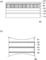
- FIG. 1 is a cross-sectional view schematically showing the structure of the first embodiment of the semiconductor light emitting device of the present invention.
- FIG. 1A is a cross-sectional view schematically showing the configuration of the semiconductor light emitting device 1.
- the semiconductor light emitting device 1 includes an n-type semiconductor layer 15, a GaN / InGaN superlattice layer 20 formed on the upper surface of the n-type semiconductor layer 15, an active layer 30 formed on the upper surface of the superlattice layer 20, and an active layer 30.
- the p-type semiconductor layer 43 is formed on the upper layer (the undoped GaN layer 41 will be described later).
- FIG. 1B is a cross-sectional view schematically showing the configuration of the superlattice layer 20
- FIG. 1C is a cross-sectional view schematically showing the configuration of the active layer 30.
- the semiconductor light emitting device 1 has a substrate 11, an undoped GaN layer 13 is formed on the upper surface of the substrate 11, and the n-type semiconductor layer 15 is formed on the upper surface of the undoped GaN layer 13.
- the substrate 11 is composed of a sapphire substrate or a GaN substrate.
- the undoped GaN layer 13 is a layer formed by epitaxial growth on the c-plane of the substrate 11 and has a thickness of, for example, 3000 nm.
- the n-type semiconductor layer 15 is formed on the upper surface of the undoped GaN layer 13.
- the n-type semiconductor layer 15 is made of AlGaN having a film thickness of 2000 nm, an Si concentration as an n-type dopant of 3 ⁇ 10 19 / cm 3 , and an Al composition of 5%.
- the superlattice layer 20 is made of GaN / InGaN and is formed on the upper surface of the n-type semiconductor layer 15.
- the superlattice layer 20 is formed by laminating the GaN layer 21 and the InGaN layer 23 with a thickness of 2.5 nm for 10 periods.
- the In composition of the InGaN layer 23 is 7%, and both the GaN layer 21 and the InGaN layer 23 are doped with a Si concentration of 1 ⁇ 10 18 / cm 3 to be n-type.
- the active layer 30 includes a first layer 31 composed of In X1 Ga 1-X1 N (0 ⁇ X1 ⁇ 0.01), In X2 Ga 1-X2 N (0.2 ⁇ X2 ⁇ 1). ) And a third layer 33 composed of Al Y1 Ga 1 -Y1 N (0 ⁇ Y1 ⁇ 1) are formed by laminating five periods.
- the first layer 31 is formed of undoped GaN with a thickness of 20 nm
- the second layer 32 is formed of undoped InGaN with a thickness of 2.6 nm and an In composition of 28%
- the third layer 33 is formed as a film. It is made of undoped AlGaN having a thickness of 1.5 nm and an Al composition of 45%.
- the first layer 31 composed of GaN or InGaN having an In ratio of 1% or less forms a barrier layer.
- the second layer 32 made of InGaN having a higher In ratio than the first layer 31 constitutes a light emitting layer.
- the third layer 33 made of AlGaN has a higher energy band gap than the first layer 31 and has a function of preventing the movement of electrons as will be described later. Demonstrate.
- an undoped GaN layer 41 is formed on the upper surface of the active layer 30. This constitutes the final barrier layer.
- the undoped GaN layer 41 may be included in the active layer 30.
- the undoped GaN layer 41 is formed with a film thickness of 20 nm, for example, like the first layer 31 in the active layer 30.
- a p-type semiconductor layer 43 is formed on the upper surface of the undoped GaN layer 41.
- the p-type semiconductor layer 43 is composed of p-GaN having a thickness of 100 nm and a Mg concentration of 3 ⁇ 10 19 / cm 3 as a p-type dopant. If necessary, a high-concentration p-type contact layer can be provided on the p-GaN.
- FIG. 2 is a cross-sectional view schematically showing the structure of a comparative example for comparison with the examples.
- symbol is attached
- subjected about the component same as FIG. 2A is a cross-sectional view schematically showing a configuration of a semiconductor light emitting device 60 of a comparative example.
- the semiconductor light emitting device 60 of the comparative example has a substrate 11, and an n-type semiconductor layer 55 is formed on the substrate 11 via an undoped GaN layer 13. Unlike the n-type semiconductor layer 15 of the embodiment, the n-type semiconductor layer 55 is made of n-GaN.
- the semiconductor light emitting device 60 of the comparative example has the InGaN / GaN superlattice layer 20 on the upper surface of the n-type semiconductor layer 55 and the active layer 50 on the upper surface of the superlattice layer 20.
- the active layer 50 has a structure in which a GaN layer 51 and an InGaN layer 52 are periodically stacked.
- the active layer 50 has five periods as in the embodiment.
- FIG. 2B is a cross-sectional view schematically showing the configuration of the active layer 50.
- the film thickness of the GaN layer 51 is 20 nm as in the first layer 31 of the example, and the film thickness of the InGaN layer 52 is 2.5 nm as in the second layer 32 of the example. That is, unlike the semiconductor light emitting device 1 of the example, the semiconductor light emitting device 60 of the comparative example does not include a layer corresponding to the third layer 33 made of AlGaN.
- the semiconductor light emitting device 60 of the comparative example includes an electron block layer 57 made of p-AlGaN on the upper surface of the active layer 50, and a p-type semiconductor layer 43 made of p-GaN on the upper surface of the electron block layer 57. Prepare.
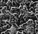
- FIG. 3A shows the surface of a GaN layer taken with a scanning electron microscope (SEM) when the Si concentration is 1.5 ⁇ 10 19 / cm 3 , but the surface is rough. It is confirmed that In addition, even when the impurity concentration was 1.3 ⁇ 10 19 / cm 3 and 2.0 ⁇ 10 19 / cm 3 , surface roughness was confirmed in the same manner.
- FIG. 3B is an image of the AlGaN layer surface taken with an AFM (Atomic Force Microscopy) when the Si concentration is 7 ⁇ 10 19 / cm 3 .
- AFM Atomic Force Microscopy
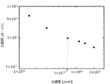
- FIG. 4 is a graph plotting the relationship between the Si concentration of AlGaN and the specific resistance when the Si concentration of AlGaN is changed at room temperature. The specific resistance was measured using a commonly used Hall measuring device.
- the specific resistance decreases as the concentration of Si doped in AlGaN increases.
- the resistance value increases due to the roughness, and therefore it is assumed that the specific resistance increases at the Si doping concentration value where the film roughness occurs. That is, according to this result, it is suggested that even when the Si concentration is increased to 2 ⁇ 10 20 / cm 3 , film roughness does not occur in AlGaN.
- the specific resistance is 5 ⁇ 10 ⁇ 3. It was ⁇ ⁇ cm. That is, when GaN is used, the specific resistance cannot be lowered more than this value.
- the semiconductor light emitting device 1 of the example since the semiconductor light emitting device 1 of the example includes the n-type semiconductor layer 15 made of AlGaN, the Si concentration can be set to 3 ⁇ 10 19 cm 3 or more.
- the lower limit value of the specific resistance can be greatly reduced.
- the element resistance can be reduced, and the necessary voltage can be reduced.
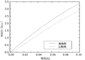
- FIG. 5 is a graph comparing the current-voltage characteristics (IV characteristics) of the semiconductor light emitting device 1 of the example and the semiconductor light emitting device 60 of the comparative example. According to FIG. 5, the same current value is realized at a lower voltage in the example than in the comparative example. Thereby, according to the semiconductor light emitting element 1 in which the n-type semiconductor layer 15 is made of AlGaN, it is understood that a sufficient amount of current is secured even under a low voltage condition, and high light emission efficiency can be realized.
- the semiconductor light emitting device 60 of the comparative example includes an electronic block layer 57. This is because electrons injected from the n-type semiconductor layer 55 into the active layer 50 enter the p-type semiconductor layer 43 beyond the active layer 50 as described above in the section “Means for Solving the Problems”. Is intended to prevent the recombination probability in the active layer 50 from decreasing.
- the electron block layer 57 is made of AlGaN having a higher energy band gap than the active layer 50 and the p-type semiconductor layer 43 in order to form a barrier against electrons flowing from the active layer 50 to the p-type semiconductor layer 43.
- the active layer 50 has the InGaN layer 52, and in order to set the peak wavelength of light generated in the active layer 50 to 530 nm or more, the In composition of the InGaN layer 52 is, for example, about 30%. Need to be increased. However, for this purpose, the growth temperature of the InGaN layer 52 needs to be lower than the general growth temperature of GaN, and this is the same even after the InGaN layer 52 is formed. That is, when forming the electron blocking layer 57, it is necessary to grow AlGaN at a low temperature within a range where the crystal of the InGaN layer 52 is not broken. However, along with this, Al is not sufficiently taken into GaN due to the parasitic reaction between the III group and the V group, pits are generated, and the film quality is deteriorated.
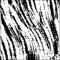
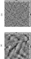
- FIG. 6 shows the case where the electron blocking layer 57 is formed after forming the active layer 50 which is a laminate of the InGaN layer 52 and the GaN layer 51 with the In composition of the InGaN layer 52 being 30%. It is the photograph which compared the surface state in the case where it does not form.
- FIG. 6A is a photograph of the surface state in a state where the active layer 50 is formed.
- FIG. 6B shows an electron blocking layer 57 made of AlGaN under a temperature condition (for example, about 880 ° C.) within a range that does not destroy the crystal state of the InGaN layer 52 after the active layer 50 is formed. It is the photograph of the formed surface state. Both are photographs taken by AFM (Atomic Force Microscopy).
- FIG. 6B shows that the number of black dots on the surface is much larger than that in FIG. 6A. This black dot corresponds to the pit. That is, it can be seen from this photograph that an extremely large number of pits are formed when AlGaN is formed as the electron block layer 57. This suggests that a parasitic reaction has occurred by growing AlGaN at a low temperature as described above.
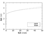
- FIG. 7 is a graph comparing the current-light output characteristics (IL characteristics) of the semiconductor light emitting device 1 of the example and the semiconductor light emitting device 60 of the comparative example. According to FIG. 7, it can be seen that the optical output of the example is higher than that of the comparative example in a state where the same current is supplied.
- IL characteristics current-light output characteristics
- the semiconductor light emitting device 60 of the comparative example has many pits (defects) formed in the electron block layer 57. For this reason, it is assumed that this pit becomes a non-light emitting center and the light emission efficiency is lowered.
- the semiconductor light emitting device 1 of the example realizes a higher light output than the semiconductor light emitting device 60 of the comparative example.
- the active layer 30 included in the semiconductor light emitting device 1 of the example includes the third layer 33 made of AlGaN, so that the overflow of electrons is suppressed without providing the electron blocking layer 57. It is a suggestion. The reason for this will be described with reference to the energy band diagrams of FIGS. 8A and 8B.
- FIG. 8A is an energy band diagram of an element (corresponding to the comparative example) that does not include the third layer 33 made of AlGaN in the active layer 50, and FIG. 8B shows an active band including the third layer 33 made of AlGaN.
- FIG. 6 is an energy band diagram of an element (corresponding to an example) including a layer 20. Both energy band diagrams show a state in which the applied bias is 0V.
- FIG. 8A for convenience of explanation, an energy band diagram of a configuration without the electron block layer 57 is shown.
- the semiconductor light emitting device 60 of the comparative example includes the electron block layer 57. However, as described above, the light output is reduced even if the electron block layer 57 is provided.
- the active layer 30 since the active layer 30 includes the third layer 33 made of AlGaN, an energy barrier due to the third layer 33 is formed in the region of the active layer 30. Yes.
- a voltage is applied to the device and electrons flowed from the n-type semiconductor layer 15 side toward the p-type semiconductor layer 43 side are taken into the well region of the second layer 32 made of InGaN, high mobility is achieved. Even if the subsequent electrons having a flow in, the barrier of the third layer 33 made of AlGaN is blocked. As a result, the probability of flowing out to the first layer 31 side composed of the upper GaN layer can be reduced.
- the third layer 33 exhibits the same barrier function as the electron blocking layer, and thus a high recombination probability is realized. .
- the third layer 33 has a very thin film thickness of about 1 nm, electrons that have not recombined can tunnel through the third layer 33, and the p-type semiconductor layer 43 side To the next second layer 32 adjacent to.
- the energy band is inclined, and the overlap between the conduction band 62 and the valence band 63 in the InGaN layer 52 is reduced.
- the overlapping degree of the wave function of electrons and holes is reduced, and even if electrons are accumulated in the well region of the InGaN layer 52, the recombination probability with holes is lowered. This also causes a decrease in light output.
- the region of the first layer 31 in FIG. 8B is compared with the region of the GaN layer 51 in FIG. 8A, but according to FIG. 8B, the bending of the energy band is suppressed compared to FIG. 8A.
- the AlGaN constituting the third layer 33 generates an electric field due to spontaneous polarization in a direction that cancels the piezoelectric field derived from InGaN constituting the second layer 32.
- the semiconductor light emitting device 1 of the example the overlapping region of the conduction band 2 and the valence band 3 in the second layer 32 is sufficiently ensured. The recombination probability of the holes can be further improved.
- the active layer 30 includes the third layer 33 made of AlGaN, so that both the function of weakening the piezoelectric field derived from InGaN and the function of suppressing the overflow of electrons are achieved. Can be made. Thereby, the probability of recombination of electrons and holes is increased without providing an electron block layer between the active layer 30 and the p-type semiconductor layer 43, and high luminous efficiency is realized.
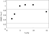
- FIG. 9 is a graph in which a plurality of semiconductor light emitting devices 1 are manufactured by changing the film thickness T1 of the first layer 31, and the relationship between the light output of each semiconductor light emitting device 1 and the film thickness T1 is plotted.
- the horizontal axis is defined by the relative value of the film thickness T1 of the first layer 31 to the film thickness T2 of the second layer 32 (ie, T1 / T2).
- the film thickness T1 of the first layer 31 is simply referred to as “film thickness T1”
- the film thickness T2 of the second layer 32 is simply referred to as “film thickness T2”.
- the light output is highest when the relative value is in the range of 5 to 10, and the light output is high when the relative value exceeds 10 and when the relative value is less than 5. It turns out that it has fallen.
- the second layer 32 made of InGaN needs to be grown at a temperature lower than a general GaN growth temperature in order to realize a high In composition.
- the first layer 31 also needs to be grown at a low temperature. For this reason, when the first layer 31 is formed, GaN must be grown at a temperature lower than the general growth temperature of GaN, and as a result, the quality of the GaN crystal is lowered.
- the first layer 31 is formed with a film thickness of a certain level or more, this crystal can grow two-dimensionally to form a good step, and the crystal quality is improved.
- FIG. 9 it can be considered that by setting T1 / T2 to 5 or more, the crystal quality of the first layer 31 is improved and high light output is realized.
- the first layer 31 is too thick, the light output is reduced due to the deterioration of the surface morphology due to the low temperature growth.
- the light output is reduced when T1 / T2 is set to 15, suggesting that the surface morphology is deteriorated under this state.
- T1 / T2 when T1 / T2 is set to 5 or more and 10 or less, the light output is not greatly reduced. Therefore, the surface morphology is not deteriorated at least in the range where T1 / T2 is 10 or less. It is guessed.
- the film thickness T1 of the first layer 31 is preferably 5 to 10 times the film thickness T2 of the second layer 32.
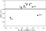
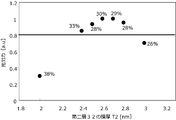
- 10A and 10B are graphs in which a plurality of semiconductor light emitting devices 1 are manufactured by changing the film thickness T2 of the second layer 32, and the relationship between the light output of each semiconductor light emitting device 1 and the film thickness T2 is plotted.
- 10A corresponds to the case where the current density supplied to the semiconductor light emitting element 1 is 25 A / cm 2
- FIG. 10B corresponds to the case where the current density supplied to the semiconductor light emitting element 1 is 50 A / cm 2.
- the numerical value written together near each plotted point has shown the value of In composition of the 2nd layer 32.
- the film thickness of the second layer 32 affects the width of the well region in the energy band diagram. Since InGaN has a strong piezoelectric field, as shown in FIG. 8B, the band of the well region formed by the second layer 32 is inclined also in the semiconductor light emitting device 1 of the example. For this reason, the band gap energy in the second layer 32 changes depending on the width of the well region, which affects the peak emission wavelength of the semiconductor light emitting device 1. That is, the peak emission wavelength of the semiconductor light emitting device 1 is affected by the In composition and the film thickness of InGaN.
- 10A and 10B show the semiconductor light emitting devices 1 manufactured by changing the film thickness and the In composition of the second layer 32 so that the peak emission wavelength is in the range of 540 nm or more and 570 nm or less.
- the optical outputs of the second layer 32 are compared according to the film thickness of the second layer 32. For example, when the film thickness of the second layer 32 is 2 nm, the In composition is 38%. When the film thickness of the second layer 32 is 2.4 nm, the In composition is 33%, and the film thickness of the second layer 32 is In the case of 3 nm, the In composition is set to 26%. However, if only the film thickness of the second layer 32 is changed, the peak emission wavelength of 540 nm or more and 570 nm or less is not realized. Indicates that it was appropriately selected.
- the light output of the semiconductor light emitting device 1 is greatly increased when the film thickness of the second layer 32 is 2.4 nm, compared to when the film thickness is 2.4 nm. Then, as the film thickness of the second layer 32 is increased to 2.5 nm and 2.6 nm, the light output of the semiconductor light emitting element 1 gradually increases, and the film thickness of the second layer 32 is further increased to 2.7 nm. As the thickness increases to 2.8 nm, the light output of the semiconductor light emitting device 1 gradually decreases. And when the film thickness of the 2nd layer 32 is 3 nm, compared with the case where the film thickness of the 2nd layer 32 is 2.8 nm, the optical output of the semiconductor light-emitting element 1 is falling significantly.
- the semiconductor light emitting device 1 is manufactured with the second layer 32 having a thickness of 2.4 nm or more and 2.8 nm or less.
- the film thickness of the second layer 32 is 2.4 nm or more and 2.8 nm or less, in order to set the peak emission wavelength of the semiconductor light emitting element 1 to 540 nm or more and 570 nm or less, the In composition of the second layer 32 is changed. It may be 28% or more and 33% or less.
- the conventional semiconductor light emitting device there is a case where Si doping is performed on the barrier layer of the active layer in order to increase the carrier injection efficiency into the active layer. is there.
- the barrier layer of the active layer here corresponds to the first layer 31 in the semiconductor light emitting device 1.
- the semiconductor light emitting device 1 it has been found that the light output is improved when the first layer 31 is formed undoped than when the first layer 31 is formed by doping Si.
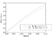
- FIG. 11 is a graph comparing the light output of (a) a semiconductor light emitting device including an undoped first layer 31 and (b) a semiconductor light emitting device 1 including a first layer 31 doped with Si.
- (a) has a higher light output under the same current supply than (b), and in the structure of the semiconductor light emitting device 1, the first layer 31 functioning as a barrier layer of the active layer 30 is It is considered that the undoped structure is preferable from the viewpoint of increasing the light output. Although this reason is not certain, as one guess, when Si doping is carried out to the whole barrier layer, it is possible that the electron overflows conversely.
- the superlattice layer 20 can be realized by a stacked body of a plurality of nitride semiconductors having different band gaps.
- the superlattice layer 20 included in the semiconductor light emitting device 1 is made of GaN / InGaN. This is an example of a stacked body of a plurality of nitride semiconductors having different band gaps.
- the superlattice layer 20 is composed of a laminate of the fourth layer 21 and the fifth layer 23 (see FIG. 1B)
- the fifth layer 23 is an InGaN layer
- the fourth layer 21 is a GaN layer.
- an InGaN layer having an In composition lower than that of the fifth layer 23 may be used.
- Step S1 An undoped GaN layer 13 is grown on the upper layer of the substrate 11.
- An example of a specific method is as follows.
- a c-plane sapphire substrate is prepared as the substrate 11 and cleaned. More specifically, for this cleaning, for example, a substrate 11 (c-plane sapphire substrate) is disposed in a processing furnace of a MOCVD (Metal Organic Chemical Vapor Deposition) apparatus, and the flow rate is set in the processing furnace. While flowing 10 slm hydrogen gas, the furnace temperature is raised to, for example, 1150 ° C.
- MOCVD Metal Organic Chemical Vapor Deposition
- an undoped GaN layer 13 is formed by forming a low-temperature buffer layer made of GaN on the surface of the substrate 11 and further forming a base layer made of GaN thereon.
- a more specific method for forming the undoped GaN layer 13 is as follows.
- the furnace pressure of the ⁇ CVD apparatus is set to 100 kPa, and the furnace temperature is set to 480 ° C. Then, while flowing nitrogen gas and hydrogen gas with a flow rate of 5 slm respectively as carrier gas into the processing furnace, trimethylgallium (TMG) with a flow rate of 50 ⁇ mol / min and ammonia with a flow rate of 250,000 ⁇ mol / min are used as the raw material gas in the processing furnace. For 68 seconds. As a result, a low-temperature buffer layer made of GaN having a thickness of 20 nm is formed on the surface of the substrate 11.
- TMG trimethylgallium
- the furnace temperature of the MOCVD apparatus is raised to 1150 ° C. Then, while flowing nitrogen gas having a flow rate of 20 slm and hydrogen gas having a flow rate of 15 slm as a carrier gas in the processing furnace, TMG having a flow rate of 100 ⁇ mol / min and ammonia having a flow rate of 250,000 ⁇ mol / min are fed into the processing furnace as source gases Feed for 60 minutes. As a result, a base layer made of GaN having a thickness of 3 ⁇ m is formed on the surface of the low-temperature buffer layer. An undoped GaN layer 13 is formed by the low-temperature buffer layer and the base layer.
- a GaN substrate can be used as the substrate 11.
- the furnace temperature of the MOCVD apparatus is set to 1050 ° C.
- the nitrogen gas having a flow rate of 20 slm as the carrier gas and the flow rate of 15 slm in the processing furnace.
- TMG having a flow rate of 100 ⁇ mol / min and ammonia having a flow rate of 250,000 ⁇ mol / min are supplied into the processing furnace for 60 minutes.
- an undoped GaN layer 13 having a thickness of 3 ⁇ m is formed on the surface of the GaN substrate.
- Step S2 the n-type semiconductor layer 15 is formed on the upper surface of the undoped GaN layer 13.
- An example of a specific method is as follows.
- the furnace pressure of the MOCVD apparatus is set to 30 kPa in a state where the furnace temperature is 1150 ° C. Then, while flowing nitrogen gas having a flow rate of 20 slm and hydrogen gas having a flow rate of 15 slm as a carrier gas into the processing furnace, TMG having a flow rate of 94 ⁇ mol / min, trimethylaluminum (TMA) having a flow rate of 6 ⁇ mol / min, Ammonia having a flow rate of 250,000 ⁇ mol / min and tetraethylsilane having a flow rate of 0.025 ⁇ mol / min for doping n-type impurities are supplied into the processing furnace for 60 minutes.
- TMG trimethylaluminum
- Ammonia having a flow rate of 250,000 ⁇ mol / min
- tetraethylsilane having a flow rate of 0.025 ⁇ mol / min for doping n-type impurities are supplied into the processing furnace for 60
- an n-type semiconductor layer 15 made of AlGaN having an Al composition of 5%, having a Si concentration of 3 ⁇ 10 19 / cm 3 and a thickness of 2 ⁇ m is formed on the upper surface of the undoped GaN layer 13.
- Step S3 a superlattice layer 20 made of GaN / InGaN is formed on the upper surface of the n-type semiconductor layer 15.
- An example of a specific method is as follows.
- the furnace pressure of the MOCVD apparatus is 100 kPa and the furnace temperature is 820 ° C. Then, while flowing nitrogen gas having a flow rate of 15 slm and hydrogen gas having a flow rate of 1 slm as a carrier gas in the processing furnace, TMG having a flow rate of 15.2 ⁇ mol / min and trimethylindium having a flow rate of 27.2 ⁇ mol / min as a source gas. (TMI) and ammonia with a flow rate of 375,000 ⁇ mol / min are supplied into the processing furnace for 54 seconds.
- a step of supplying TMG having a flow rate of 15.2 ⁇ mol / min and ammonia having a flow rate of 375000 ⁇ mol / min into the processing furnace for 54 seconds is performed.
- a superlattice layer 20 in which an InGaN layer 23 with an In composition of 7% with a thickness of 2.5 nm and a GaN layer 21 with a thickness of 2.5 nm are stacked in 10 cycles is obtained as n It is formed on the upper surface of the type semiconductor layer 15.
- the superlattice layer 20 can also be configured as a stacked body of InGaN having a low In composition and InGaN having a high In composition.
- this step S3 while flowing nitrogen gas with a flow rate of 15 slm and hydrogen gas with a flow rate of 1 slm, TMG with a flow rate of 15.2 ⁇ mol / min, TMI with a flow rate of 27.2 ⁇ mol / min, A step of supplying ammonia with a flow rate of 375,000 ⁇ mol / min into the processing furnace for 54 seconds, TMG with a flow rate of 15.2 ⁇ mol / min, TMI with a flow rate of 1 ⁇ mol / min, and ammonia with a flow rate of 375000 ⁇ mol / min into the processing furnace The step of supplying for 2 seconds is performed.
- an InGaN layer 23 having an In composition of 7% having a thickness of 2.5 nm and an InGaN layer 21 having an In composition of 1% or less having a thickness of 2.5 nm are stacked in 10 cycles.
- a lattice layer 20 is formed on the upper surface of the n-type semiconductor layer 15.
- Step S4 Next, on the upper surface of the superlattice layer 20, a first layer 31 composed of In X1 Ga 1-X1 N (0 ⁇ X1 ⁇ 0.01), In X2 Ga 1-X2 N (0.2 ⁇ X2 ⁇ A second layer 32 constituted by 1) and a third layer 33 constituted by Al Y1 Ga 1 -Y1 N (0 ⁇ Y1 ⁇ 1) are formed.
- Step S4 is configured by executing step S4a for forming the second layer 32, step S4b for forming the third layer 33, and step S4c for forming the first layer 31 a plurality of times.
- the furnace pressure of the MOCVD apparatus is 100 kPa
- the furnace temperature is 700 ° C. to 830 ° C.
- the flow rate is 15 slm nitrogen gas
- the flow rate is 1 slm hydrogen gas
- the flow rate is 375000 ⁇ mol / min.
- Ammonia is continuously fed into the processing furnace.
- Step S4a Under a state where the furnace temperature is 700 ° C. and hydrogen gas, nitrogen gas, and ammonia are continuously supplied at the above flow rates, TMI with a flow rate of 27.2 ⁇ mol / min and TMG with a flow rate of 15.2 ⁇ mol / min are applied for 54 seconds. Supply. As a result, a second layer 32 having a thickness of 2.6 nm made of undoped InGaN having an In composition of 28% is formed.
- Step S4b Subsequently, TMG having a flow rate of 15.2 ⁇ mol / min and TMA having a flow rate of 17.3 ⁇ mol / min were set under the condition that the furnace temperature was 700 ° C. and hydrogen gas, nitrogen gas, and ammonia were continuously supplied at the above-described flow rates. Feed continuously for 30 seconds. As a result, the third layer 33 having a thickness of 1.5 nm and made of undoped AlGaN having an Al composition of 45% is formed.
- Step S4c TMG with a flow rate of 15.2 ⁇ mol / min was continuously supplied for 60 seconds under a state where the furnace temperature was 700 ° C. and hydrogen gas, nitrogen gas, and ammonia were continuously supplied at the above-described flow rates. A 3 nm GaN layer is formed. Next, the furnace temperature is raised to 830 ° C. TMG is continuously supplied for 340 seconds at the same gas flow rate while maintaining this temperature rising process and the temperature, thereby forming a GaN layer having a thickness of 17 nm. As a result, a GaN layer having a thickness of 20 nm is formed as the first layer 31.
- the first layer 31 is made of InGaN having a low In composition, it is formed by the following method instead of the above. That is, TMG having a flow rate of 1 ⁇ mol / min and a flow rate of 15.2 ⁇ mol / min is supplied for 400 seconds in a state where hydrogen gas, nitrogen gas, and ammonia are continuously supplied at the same flow rate as in step S4b. As a result, a first layer 31 having a thickness of 20 nm and made of undoped InGaN having an In composition of 1% or less is formed.
- the active layer 30 in which the first layer 31, the second layer 32, and the third layer 33 are stacked for five periods is formed by repeatedly executing the above steps S4a to S4c five times.
- the growth rate In the process of growing InGaN, it is preferable to set the growth rate to about 3 nm / min from the viewpoint of suppressing droplets as much as possible and promoting migration.
- Step S5 On the upper surface of the active layer 30, an undoped GaN layer 41 is formed with a film thickness of 20 nm, for example.
- the undoped GaN layer 41 finally executes step S4c and ends step S4 when the active layer 30 is formed in step S4.
- the GaN layer formed in step S4c can be an undoped GaN layer 41.
- the first layer 31 is composed of InGaN with a low In composition, it is formed in this step S4c by executing step S4c with the TMI supply stopped and ending step S4.
- the GaN layer 41 can be an undoped GaN layer 41.
- Step S6 A p-type semiconductor layer 43 is formed on the upper surface of the undoped GaN layer 41.
- a specific method is as follows.
- the furnace pressure of the MOCVD apparatus is maintained at 100 kPa, and the furnace temperature is raised to 930 ° C. while nitrogen gas having a flow rate of 15 slm and hydrogen gas having a flow rate of 25 slm are allowed to flow into the processing furnace. Thereafter, as source gas, TMG having a flow rate of 100 ⁇ mol / min, ammonia having a flow rate of 250,000 ⁇ mol / min, and biscyclopentadienyl magnesium (Cp 2 Mg) having a flow rate of 0.1 ⁇ mol / min for doping p-type impurities. ) Is fed into the processing furnace for 360 seconds.
- a p-type semiconductor layer 43 made of GaN having a thickness of 120 nm is formed on the upper surface of the undoped GaN layer 41.
- the p-type impurity (Mg) concentration of the p-type semiconductor layer 43 is about 3 ⁇ 10 19 / cm 3 .
- a contact layer made of a high-concentration p-type GaN layer having a thickness of 5 nm may be formed by continuously changing the flow rate of Cp2Mg to 0.3 ⁇ mol / min and supplying a source gas for 20 seconds.
- the contact layer is also included in the p-type semiconductor layer 43.
- the contact layer has a p-type impurity (Mg) concentration of about 1 ⁇ 10 20 / cm 3 .
- the said embodiment demonstrated the case where the p-type impurity contained in the p-type semiconductor layer 43 was Mg, Be, Zn, and C other than Mg can be used.
- the lateral structure semiconductor light emitting device 1 a part of the upper surface of the n-type semiconductor layer 15 is exposed by ICP etching, an n-side electrode is formed on the exposed upper layer of the n-type semiconductor layer 15, and a p-type semiconductor layer is formed. A p-side electrode is formed on the upper layer 43. And each element is isolate
- the “lateral structure” means that the n-side electrode formed in the upper layer of the n-type semiconductor layer 15 and the p-side electrode formed in the upper layer of the p-type semiconductor layer 43 are in the same direction with respect to the substrate. It refers to the structure formed.
- the semiconductor light emitting device 1 having a so-called “vertical structure”
- a metal electrode (reflective electrode), a solder diffusion layer, and a solder layer serving as a p-side electrode are formed on the p-type semiconductor layer 43.
- the support substrate for example, CuW board
- substrate 11 is peeled by methods, such as a laser irradiation, upside down.
- an n-side electrode is formed on the n-type semiconductor layer 15.
- element isolation and wire bonding are performed as in the horizontal structure.
- the “vertical structure” refers to a structure in which an n-side electrode and a p-side electrode are formed in opposite directions across a substrate.
- FIG. 12 is a cross-sectional view schematically showing the structure of the second embodiment of the semiconductor light emitting device.
- the semiconductor light emitting device 1a shown in FIG. 12 is different from the semiconductor light emitting device 1 shown in FIG. 1 only in that a hole barrier layer 17 is further provided between the superlattice layer 20 and the active layer 30, and the others are common. It is.
- the hole barrier layer 17 is composed of a nitride semiconductor layer doped with Si. The function of the hole blocking layer 17 will be described by comparing the energy band diagram of the semiconductor light emitting device 1a shown in FIG. 13 with the energy band diagram of the semiconductor light emitting device 1 shown in FIG. 8B.
- the band has an inclination between the superlattice layer 20 and the active layer 30.
- the energy band gap is widened between the superlattice layer 20 and the active layer 30 due to the presence of the hole barrier layer 17, and the superlattice layer It can be seen that the band diagram between 20 and the active layer 30 is flattened.
- a groove is formed in the band diagram of the valence band of the active layer in the vicinity of the joint surface of the third layer 33 and the first layer 31, and the groove is positively connected.
- the holes are accumulated two-dimensionally (two-dimensional hole gas). Since this hole has high mobility in the two-dimensional direction, the hole injected from the p-type semiconductor layer 43 side into the active layer 30 exceeds the active layer 30 without recombining with electrons. There is a possibility that a phenomenon will occur.
- the holes are accumulated in the well region formed of InGaN in the GaN / InGaN superlattice layer 20 formed between the active layer and the n-type semiconductor layer.
- electrons injected from the n-type semiconductor layer 15 recombine with holes in the superlattice layer 20 to generate light with a wavelength other than desired.
- light having a peak wavelength different from the peak wavelength of light generated in the active layer is generated, which is not preferable.
- the band diagram can be flattened as the nitride semiconductor layer constituting the hole barrier layer 17 is doped with Si at a higher concentration.
- Si concentration exceeds 5 ⁇ 10 19 / cm 3
- surface roughness of the nitride semiconductor layer appears, so that the Si concentration is set to 5 ⁇ 10 18 / cm 3 or more and 5 ⁇ 10 19 / cm 3 or less. Is preferred.
- Si concentration is lower than 5 ⁇ 10 18 / cm 3 , the effect of suppressing the overflow of holes is low.
- a hole barrier is required. It is preferable to use AlGaN as the layer 17. GaN may be used as long as it is within a Si concentration range of less than 1 ⁇ 10 19 / cm 3 .
- step S3A for forming the hole barrier layer 17 may be further added between step S3 and step S4.
- Step S3A After performing steps S1 to S3 as in the first embodiment, with the furnace temperature kept at 820 ° C., the flow rate was 15.2 ⁇ mol / min TMG, the flow rate was 1 ⁇ mol / min TMA, and the flow rate was 0.002 ⁇ mol.
- a step of supplying / ethyl tetraethylsilane / min and ammonia having a flow rate of 375000 ⁇ mol / min into the processing furnace for 400 seconds is performed. Thereby, an AlGaN layer as the hole barrier layer 17 having a Si concentration of 3 ⁇ 10 19 / cm 3 , a thickness of 20 nm, and an Al composition of 6% is formed on the upper surface of the superlattice layer 20.
- step S4 Since the manufacturing process after step S4 is the same as that of the first embodiment, the description is omitted.
- ⁇ Third embodiment> A third embodiment of the semiconductor light emitting device of the present invention will be described. Note that the third embodiment is different from the first embodiment only in the configuration of the active layer 30, and the other is common to the first embodiment or the second embodiment.
- the third layer 33 made of AlGaN is provided over the entire period of the active layer 30.
- the third layer 33 may not be provided in every cycle.
- the active layer 30 includes the third layer 33 only at a position close to the p-type semiconductor layer 43 and does not include the third layer 33 at a position close to the n-type semiconductor layer 15. .
- the first layer 31, the second layer 32, and the third layer 33 are periodically formed at a position near the p-type semiconductor layer 43, and the first layer 31, the second layer 32, and the third layer 33 are formed at a position near the n-type semiconductor layer 15.
- the first layer 31 and the second layer 32 are formed periodically.
- FIG. 14 shows the configuration of the semiconductor light emitting device 1 a according to the second embodiment.
- the third layer 33 is provided only at a position close to the p-type semiconductor layer 43, and the third layer 33 is provided at a position close to the n-type semiconductor layer 15. It is an energy band figure at the time of setting it as a structure which is not. Similar to the semiconductor light emitting device 1 whose energy band diagram is shown in FIG. 13, the active layer 30 has a five-period structure. However, for the two periods near the n-type semiconductor layer 15, the active layer 30 has a first layer 31 and a second layer 32. For the three periods close to the p-type semiconductor layer 43, the active layer 30 has a periodic structure of the first layer 31, the second layer 32, and the third layer 33, as shown in FIG.
- the third layer 33 made of AlGaN has an energy band gap larger than that of the first layer 31 made of GaN (or InGaN having a low In composition)
- electrons are on the p-type semiconductor layer 43 side. It constitutes an energy barrier when moving to.
- an energy barrier is also formed by the third layer 33 in the vicinity of the n-type semiconductor layer 15.
- the electrons supplied from the n-type semiconductor layer 15 are prevented from moving by this energy barrier formed at a position close to the n-type semiconductor layer 15, and the electrons are placed in the well region constituted by the second layer 32. There is a possibility that the probability of being captured will decrease.
- the third layer 33 does not exist in the active layer 30 in the region formed on the n-type semiconductor layer 15 side, and therefore there is a high energy barrier that prevents the movement of electrons. do not do. Therefore, when a voltage is applied to the semiconductor light emitting device 1, electrons flow into the active layer 30 with a high probability up to the place where the third layer 33 is formed. Then, movement of some electrons is blocked by the energy barrier of the third layer 33, so that electrons can be taken into the well region formed by the second layer 32 with high probability. As a result, electrons and holes can be recombined with high probability in the well region. That is, the light emitting efficiency can be improved by using the element configuration shown in the energy band diagram of FIG. 14 as compared with the element configuration shown in the energy band diagram of FIG.
- steps S4a and S4c may be repeatedly executed in the initial stage of step S4, and then steps S4a, S4b, and S4c may be repeatedly executed. Other steps are the same as those described above.
- the third layer 33 is provided only at a position close to the p-type semiconductor layer 43, The third layer 33 may not be provided at a position close to the n-type semiconductor layer 15.
Landscapes
- Led Devices (AREA)
Priority Applications (2)
| Application Number | Priority Date | Filing Date | Title |
|---|---|---|---|
| US15/116,268 US20170012166A1 (en) | 2014-02-05 | 2015-02-02 | Semiconductor light-emitting element |
| CN201580005053.5A CN105917478A (zh) | 2014-02-05 | 2015-02-02 | 半导体发光元件 |
Applications Claiming Priority (2)
| Application Number | Priority Date | Filing Date | Title |
|---|---|---|---|
| JP2014020387A JP5861947B2 (ja) | 2014-02-05 | 2014-02-05 | 半導体発光素子及びその製造方法 |
| JP2014-020387 | 2014-09-16 |
Publications (1)
| Publication Number | Publication Date |
|---|---|
| WO2015119066A1 true WO2015119066A1 (ja) | 2015-08-13 |
Family
ID=53777871
Family Applications (1)
| Application Number | Title | Priority Date | Filing Date |
|---|---|---|---|
| PCT/JP2015/052791 Ceased WO2015119066A1 (ja) | 2014-02-05 | 2015-02-02 | 半導体発光素子 |
Country Status (4)
| Country | Link |
|---|---|
| US (1) | US20170012166A1 (enExample) |
| JP (1) | JP5861947B2 (enExample) |
| CN (1) | CN105917478A (enExample) |
| WO (1) | WO2015119066A1 (enExample) |
Cited By (2)
| Publication number | Priority date | Publication date | Assignee | Title |
|---|---|---|---|---|
| TWI738790B (zh) * | 2016-08-31 | 2021-09-11 | 國立硏究開發法人科學技術振興機構 | 化合物半導體及其製造方法以及氮化物半導體 |
| US11888033B2 (en) | 2017-06-01 | 2024-01-30 | Japan Science And Technology Agency | Compound semiconductor and method for manufacturing same |
Families Citing this family (6)
| Publication number | Priority date | Publication date | Assignee | Title |
|---|---|---|---|---|
| JP6135954B2 (ja) * | 2015-10-22 | 2017-05-31 | ウシオ電機株式会社 | 窒化物半導体発光素子 |
| DE102016112294A1 (de) | 2016-07-05 | 2018-01-11 | Osram Opto Semiconductors Gmbh | Halbleiterschichtenfolge |
| DE102017109804A1 (de) * | 2017-05-08 | 2018-11-08 | Osram Opto Semiconductors Gmbh | Halbleiterlaser |
| JP6438542B1 (ja) * | 2017-07-27 | 2018-12-12 | 日機装株式会社 | 半導体発光素子 |
| JP7149486B2 (ja) * | 2020-04-21 | 2022-10-07 | 日亜化学工業株式会社 | 発光素子の製造方法 |
| JP2025017479A (ja) * | 2023-07-25 | 2025-02-06 | 日機装株式会社 | 窒化物半導体発光素子 |
Citations (5)
| Publication number | Priority date | Publication date | Assignee | Title |
|---|---|---|---|---|
| JP2001102675A (ja) * | 1999-09-29 | 2001-04-13 | Toshiba Corp | 半導体発光素子 |
| JP2001237457A (ja) * | 1999-12-13 | 2001-08-31 | Nichia Chem Ind Ltd | 発光素子 |
| JP2006261392A (ja) * | 2005-03-17 | 2006-09-28 | Matsushita Electric Ind Co Ltd | 窒化ガリウム系化合物半導体発光ダイオードおよび照明装置 |
| JP2009272606A (ja) * | 2008-05-09 | 2009-11-19 | Samsung Electro Mech Co Ltd | 窒化物半導体発光素子 |
| JP2012178386A (ja) * | 2011-02-25 | 2012-09-13 | Toshiba Corp | 半導体発光素子 |
Family Cites Families (2)
| Publication number | Priority date | Publication date | Assignee | Title |
|---|---|---|---|---|
| KR100631971B1 (ko) * | 2005-02-28 | 2006-10-11 | 삼성전기주식회사 | 질화물 반도체 발광 소자 |
| JP5549338B2 (ja) * | 2010-04-09 | 2014-07-16 | ウシオ電機株式会社 | 紫外光放射用窒素化合物半導体ledおよびその製造方法 |
-
2014
- 2014-02-05 JP JP2014020387A patent/JP5861947B2/ja active Active
-
2015
- 2015-02-02 CN CN201580005053.5A patent/CN105917478A/zh active Pending
- 2015-02-02 WO PCT/JP2015/052791 patent/WO2015119066A1/ja not_active Ceased
- 2015-02-02 US US15/116,268 patent/US20170012166A1/en not_active Abandoned
Patent Citations (5)
| Publication number | Priority date | Publication date | Assignee | Title |
|---|---|---|---|---|
| JP2001102675A (ja) * | 1999-09-29 | 2001-04-13 | Toshiba Corp | 半導体発光素子 |
| JP2001237457A (ja) * | 1999-12-13 | 2001-08-31 | Nichia Chem Ind Ltd | 発光素子 |
| JP2006261392A (ja) * | 2005-03-17 | 2006-09-28 | Matsushita Electric Ind Co Ltd | 窒化ガリウム系化合物半導体発光ダイオードおよび照明装置 |
| JP2009272606A (ja) * | 2008-05-09 | 2009-11-19 | Samsung Electro Mech Co Ltd | 窒化物半導体発光素子 |
| JP2012178386A (ja) * | 2011-02-25 | 2012-09-13 | Toshiba Corp | 半導体発光素子 |
Cited By (3)
| Publication number | Priority date | Publication date | Assignee | Title |
|---|---|---|---|---|
| TWI738790B (zh) * | 2016-08-31 | 2021-09-11 | 國立硏究開發法人科學技術振興機構 | 化合物半導體及其製造方法以及氮化物半導體 |
| US11549172B2 (en) | 2016-08-31 | 2023-01-10 | Japan Science And Technology Agency | Compound semiconductor, method for manufacturing same, and nitride semiconductor |
| US11888033B2 (en) | 2017-06-01 | 2024-01-30 | Japan Science And Technology Agency | Compound semiconductor and method for manufacturing same |
Also Published As
| Publication number | Publication date |
|---|---|
| CN105917478A (zh) | 2016-08-31 |
| US20170012166A1 (en) | 2017-01-12 |
| JP2015149342A (ja) | 2015-08-20 |
| JP5861947B2 (ja) | 2016-02-16 |
Similar Documents
| Publication | Publication Date | Title |
|---|---|---|
| JP5861947B2 (ja) | 半導体発光素子及びその製造方法 | |
| TWI478383B (zh) | 半導體發光裝置 | |
| US7663138B2 (en) | Nitride semiconductor light emitting element | |
| JP2008288397A (ja) | 半導体発光装置 | |
| JP6128138B2 (ja) | 半導体発光素子 | |
| JP5983684B2 (ja) | Led素子 | |
| US9818907B2 (en) | LED element | |
| US20170338378A1 (en) | Method of producing iii nitride semiconductor light-emitting device and iii nitride semiconductor light-emitting device | |
| JP6135954B2 (ja) | 窒化物半導体発光素子 | |
| JP5800251B2 (ja) | Led素子 | |
| JP2008227103A (ja) | GaN系半導体発光素子 | |
| JP5800252B2 (ja) | Led素子 | |
| JP6884505B2 (ja) | 半導体発光素子およびその製造方法 | |
| JP2007200933A (ja) | 窒化物系半導体素子の製造方法 | |
| JP2008118048A (ja) | GaN系半導体発光素子 | |
| US10038118B2 (en) | Light emitting element | |
| JP2012256948A (ja) | 半導体発光素子 | |
| WO2014115800A1 (ja) | Led素子 | |
| JP2016111079A (ja) | 半導体発光素子 |
Legal Events
| Date | Code | Title | Description |
|---|---|---|---|
| 121 | Ep: the epo has been informed by wipo that ep was designated in this application |
Ref document number: 15746264 Country of ref document: EP Kind code of ref document: A1 |
|
| WWE | Wipo information: entry into national phase |
Ref document number: 15116268 Country of ref document: US |
|
| NENP | Non-entry into the national phase |
Ref country code: DE |
|
| 122 | Ep: pct application non-entry in european phase |
Ref document number: 15746264 Country of ref document: EP Kind code of ref document: A1 |