WO2015115249A1 - 構造体および成膜方法 - Google Patents
構造体および成膜方法 Download PDFInfo
- Publication number
- WO2015115249A1 WO2015115249A1 PCT/JP2015/051373 JP2015051373W WO2015115249A1 WO 2015115249 A1 WO2015115249 A1 WO 2015115249A1 JP 2015051373 W JP2015051373 W JP 2015051373W WO 2015115249 A1 WO2015115249 A1 WO 2015115249A1
- Authority
- WO
- WIPO (PCT)
- Prior art keywords
- film
- thin film
- metal thin
- sputtering
- film forming
- Prior art date
- Legal status (The legal status is an assumption and is not a legal conclusion. Google has not performed a legal analysis and makes no representation as to the accuracy of the status listed.)
- Ceased
Links
Images







Classifications
-
- C—CHEMISTRY; METALLURGY
- C23—COATING METALLIC MATERIAL; COATING MATERIAL WITH METALLIC MATERIAL; CHEMICAL SURFACE TREATMENT; DIFFUSION TREATMENT OF METALLIC MATERIAL; COATING BY VACUUM EVAPORATION, BY SPUTTERING, BY ION IMPLANTATION OR BY CHEMICAL VAPOUR DEPOSITION, IN GENERAL; INHIBITING CORROSION OF METALLIC MATERIAL OR INCRUSTATION IN GENERAL
- C23C—COATING METALLIC MATERIAL; COATING MATERIAL WITH METALLIC MATERIAL; SURFACE TREATMENT OF METALLIC MATERIAL BY DIFFUSION INTO THE SURFACE, BY CHEMICAL CONVERSION OR SUBSTITUTION; COATING BY VACUUM EVAPORATION, BY SPUTTERING, BY ION IMPLANTATION OR BY CHEMICAL VAPOUR DEPOSITION, IN GENERAL
- C23C14/00—Coating by vacuum evaporation, by sputtering or by ion implantation of the coating forming material
- C23C14/02—Pretreatment of the material to be coated
- C23C14/024—Deposition of sublayers, e.g. to promote adhesion of the coating
-
- C—CHEMISTRY; METALLURGY
- C22—METALLURGY; FERROUS OR NON-FERROUS ALLOYS; TREATMENT OF ALLOYS OR NON-FERROUS METALS
- C22C—ALLOYS
- C22C21/00—Alloys based on aluminium
-
- C—CHEMISTRY; METALLURGY
- C23—COATING METALLIC MATERIAL; COATING MATERIAL WITH METALLIC MATERIAL; CHEMICAL SURFACE TREATMENT; DIFFUSION TREATMENT OF METALLIC MATERIAL; COATING BY VACUUM EVAPORATION, BY SPUTTERING, BY ION IMPLANTATION OR BY CHEMICAL VAPOUR DEPOSITION, IN GENERAL; INHIBITING CORROSION OF METALLIC MATERIAL OR INCRUSTATION IN GENERAL
- C23C—COATING METALLIC MATERIAL; COATING MATERIAL WITH METALLIC MATERIAL; SURFACE TREATMENT OF METALLIC MATERIAL BY DIFFUSION INTO THE SURFACE, BY CHEMICAL CONVERSION OR SUBSTITUTION; COATING BY VACUUM EVAPORATION, BY SPUTTERING, BY ION IMPLANTATION OR BY CHEMICAL VAPOUR DEPOSITION, IN GENERAL
- C23C14/00—Coating by vacuum evaporation, by sputtering or by ion implantation of the coating forming material
- C23C14/06—Coating by vacuum evaporation, by sputtering or by ion implantation of the coating forming material characterised by the coating material
- C23C14/14—Metallic material, boron or silicon
- C23C14/20—Metallic material, boron or silicon on organic substrates
- C23C14/205—Metallic material, boron or silicon on organic substrates by cathodic sputtering
-
- C—CHEMISTRY; METALLURGY
- C23—COATING METALLIC MATERIAL; COATING MATERIAL WITH METALLIC MATERIAL; CHEMICAL SURFACE TREATMENT; DIFFUSION TREATMENT OF METALLIC MATERIAL; COATING BY VACUUM EVAPORATION, BY SPUTTERING, BY ION IMPLANTATION OR BY CHEMICAL VAPOUR DEPOSITION, IN GENERAL; INHIBITING CORROSION OF METALLIC MATERIAL OR INCRUSTATION IN GENERAL
- C23C—COATING METALLIC MATERIAL; COATING MATERIAL WITH METALLIC MATERIAL; SURFACE TREATMENT OF METALLIC MATERIAL BY DIFFUSION INTO THE SURFACE, BY CHEMICAL CONVERSION OR SUBSTITUTION; COATING BY VACUUM EVAPORATION, BY SPUTTERING, BY ION IMPLANTATION OR BY CHEMICAL VAPOUR DEPOSITION, IN GENERAL
- C23C16/00—Chemical coating by decomposition of gaseous compounds, without leaving reaction products of surface material in the coating, i.e. chemical vapour deposition [CVD] processes
- C23C16/22—Chemical coating by decomposition of gaseous compounds, without leaving reaction products of surface material in the coating, i.e. chemical vapour deposition [CVD] processes characterised by the deposition of inorganic material, other than metallic material
- C23C16/30—Deposition of compounds, mixtures or solid solutions, e.g. borides, carbides, nitrides
- C23C16/40—Oxides
- C23C16/401—Oxides containing silicon
- C23C16/402—Silicon dioxide
-
- C—CHEMISTRY; METALLURGY
- C23—COATING METALLIC MATERIAL; COATING MATERIAL WITH METALLIC MATERIAL; CHEMICAL SURFACE TREATMENT; DIFFUSION TREATMENT OF METALLIC MATERIAL; COATING BY VACUUM EVAPORATION, BY SPUTTERING, BY ION IMPLANTATION OR BY CHEMICAL VAPOUR DEPOSITION, IN GENERAL; INHIBITING CORROSION OF METALLIC MATERIAL OR INCRUSTATION IN GENERAL
- C23C—COATING METALLIC MATERIAL; COATING MATERIAL WITH METALLIC MATERIAL; SURFACE TREATMENT OF METALLIC MATERIAL BY DIFFUSION INTO THE SURFACE, BY CHEMICAL CONVERSION OR SUBSTITUTION; COATING BY VACUUM EVAPORATION, BY SPUTTERING, BY ION IMPLANTATION OR BY CHEMICAL VAPOUR DEPOSITION, IN GENERAL
- C23C16/00—Chemical coating by decomposition of gaseous compounds, without leaving reaction products of surface material in the coating, i.e. chemical vapour deposition [CVD] processes
- C23C16/44—Chemical coating by decomposition of gaseous compounds, without leaving reaction products of surface material in the coating, i.e. chemical vapour deposition [CVD] processes characterised by the method of coating
- C23C16/50—Chemical coating by decomposition of gaseous compounds, without leaving reaction products of surface material in the coating, i.e. chemical vapour deposition [CVD] processes characterised by the method of coating using electric discharges
- C23C16/505—Chemical coating by decomposition of gaseous compounds, without leaving reaction products of surface material in the coating, i.e. chemical vapour deposition [CVD] processes characterised by the method of coating using electric discharges using radio frequency discharges
-
- G—PHYSICS
- G02—OPTICS
- G02B—OPTICAL ELEMENTS, SYSTEMS OR APPARATUS
- G02B5/00—Optical elements other than lenses
- G02B5/08—Mirrors
- G02B5/0808—Mirrors having a single reflecting layer
Definitions
- the present invention relates to a structure in which a resin and a metal thin film are laminated and a film forming method for forming a metal thin film on a resin workpiece.
- an inorganic material substrate such as glass has been conventionally used.
- replacement with a resin base material is progressing due to the demand for weight reduction for the purpose of improving the fuel efficiency of automobiles.
- a plating method has been frequently used for forming a metal film.
- replacement with a dry process such as a sputtering method has been advanced in order to reduce the environmental load. For this reason, with respect to such a component, film formation by sputtering using a metal such as aluminum as a target is performed on an injection molded resin product for the purpose of providing a mirror finish or a metallic texture.
- film formation of a silicon oxide protective film or the like by plasma CVD is often performed in order to prevent oxidation of the metal film or protect the surface from scratches. That is, the workpiece after film formation by sputtering is transferred to another film formation apparatus, and plasma CVD using a monomer gas such as HMDSO (hexa-methyl-di-siloxane) is performed in the chamber of the film formation apparatus.
- a protective film is formed on the surface after the film formation by sputtering.
- Patent Document 1 discloses a film forming apparatus in which a sputtering electrode and a composite film forming or polymerization film forming electrode are arranged at positions separated by a predetermined distance.
- a work and a sputtering electrode are arranged to face each other, and after introducing an inert gas into the chamber, direct current is applied to the sputtering electrode to perform film formation by sputtering.
- the film forming apparatus described in Patent Document 1 has a configuration in which a shutter is arranged on a target that is not used.
- methacrylic (PMMA) resin is not only inexpensive, but is often used for mirrors and the like because of its high transparency, and has a high-class feeling depending on the transparency. For this reason, there is a high demand for use in cosmetic containers.
- methacrylic resin has low adhesion to a metal thin film, and it is difficult to form an appropriate metal thin film on the surface thereof.
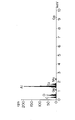
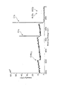
- FIG. 19 is a graph showing a wide scan spectrum in which the elemental composition exposed on the back surface of the methacrylic resin peeled off from the Al film is measured by X-ray photoelectron spectroscopy (XPS).
- XPS X-ray photoelectron spectroscopy
- the horizontal axis in FIG. 19 represents the binding energy (Binding Energy), and the vertical axis represents the count number (CPS).
- the detection depth in XPS analysis is in the range of several nm (nanometer) to 10 nm from the surface, so that the surface of the exfoliated part is the embrittled part of the methacrylic resin surface, and Al is exfoliated. It exists in the deeper area
- embrittled portions are caused by the introduction power applied to the sputter electrode during sputtering, as in the case where an input power of 25 watts or more per square centimeter is applied to the surface area of the target material in the sputter electrode. It has been found by the present inventor that it becomes particularly prominent when enlarged.
- the present invention has been made to solve the above problems, and even when a resin having low adhesion to a metal thin film such as a methacrylic resin is used, the resin and the metal thin film are firmly adhered and laminated.
- a film forming method capable of manufacturing a structure and a structure in which a metal thin film is formed with high adhesion to a resin workpiece having low adhesion to the metal thin film.
- 1st invention is the structure by which resin and the metal thin film were laminated
- the mixed region in the mixed region, at least one of O or C is mixed together with atoms and Si constituting the metal thin film.
- the resin is a methacrylic resin.
- the metal thin film is formed by a sputtering method.
- the metal thin film is made of Al or a metal containing Al as a main component.
- the metal thin film is formed by sputtering after performing plasma processing in the presence of Si, a mixed region in which Al and Si are mixed is formed.
- an atom constituting the metal thin film is covalently bonded to any one of Si, O, and C, or an atom constituting the metal thin film is any of Si, O, and C.
- a heel diffusion alloy layer is formed.
- a mixed layer of Si, O, and C a compound layer containing Si oxide, an atom constituting the metal thin film, Si, and O between the resin and the metal thin film.
- the mixed layers are stacked in this order.
- a mixed layer of Si, O, and C and a mixed layer of atoms, Si, and O constituting the metal thin film are laminated in this order between the resin and the metal thin film.
- a protective film is further formed on the surface of the metal thin film.
- the protective film is a Si oxide based protective film.
- a twelfth aspect of the present invention is a film forming method for forming a metal thin film on a resin workpiece, the plasma processing step for performing plasma processing in the presence of Si on the resin workpiece, and the workpiece A sputtering film forming step of performing sputtering film formation with a metal target material.
- a thirteenth aspect of the invention is a workpiece carrying-in step of loading the workpiece into a chamber, an inert gas supplying step of supplying an inert gas containing Si into the chamber, and a CVD for forming a film containing Si by plasma CVD. And a sputtering film forming step of forming a metal thin film by sputtering.
- a fourteenth aspect of the invention is a workpiece loading step of loading the workpiece into the chamber, an oxygen supply step of supplying oxygen containing Si into the chamber, a CVD step of forming a film containing Si by plasma CVD, and sputtering. And a sputtering film forming step of forming a metal thin film.
- the fifteenth aspect of the invention includes a Si oxide plasma CVD film forming step before the plasma processing step or between the plasma processing step and the sputtering film forming step.
- the sixteenth aspect of the invention includes a source gas supply step of supplying a source gas into the chamber and a step of forming a film containing the source gas by plasma CVD after the sputtering film forming step.
- the resin and the metal thin film can be firmly adhered and laminated. It becomes.
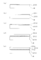
- FIG. 3 is a schematic diagram illustrating a film formation state on a workpiece W.
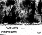
- FIG. 4 is a photograph of a cross section of a region from a workpiece W to an Al thin film 102 taken using a transmission electron microscope when film formation is performed by applying the film formation method according to the present invention.
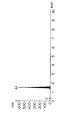
- 6 is a graph showing a TEM-EDX analysis result of a point 1-1 portion in FIG. 6 is a graph showing a TEM-EDX analysis result of a point 1-2 portion in FIG.
- FIG. 6 is a graph showing a TEM-EDX analysis result of a point 1-3 portion in FIG. It is the photograph which image
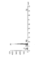
- 10 is a graph showing a TEM-EDX analysis result of a point 2-1 portion in FIG. 10 is a graph showing a TEM-EDX analysis result of a point 2-2 portion in FIG. 10 is a graph showing a TEM-EDX analysis result of a point 2-3 portion in FIG. It is a flowchart which shows the film-forming operation
- FIG. 3 is a schematic diagram illustrating a film formation state on a workpiece W.
- FIG. It is a flowchart which shows the film-forming operation
- 3 is a schematic diagram illustrating a film formation state on a workpiece W.
- FIG. It is a schematic diagram of the film-forming apparatus for performing the film-forming method concerning 4th Embodiment of this invention. It is a flowchart which shows the film-forming operation
- FIG. 1 is a schematic diagram of a film forming apparatus for executing the film forming method according to the present invention.
- the film forming apparatus performs film formation by sputtering and film formation by plasma CVD on a resin workpiece W.
- methacrylic resin is used as the material of the workpiece W.
- the methacrylic resin is a formal name of a resin generally called an acrylic resin, and may be called PMMA (polymethyl methacrylate resin) or acrylic glass.
- PMMA polymethyl methacrylate resin
- the methacrylic resin is not only inexpensive, but also has a characteristic that it has high transparency and a low adhesion to the metal thin film.
- This film forming apparatus includes a film forming chamber 10 including a main body 11 and an opening / closing part 12.
- the opening / closing part 12 moves between a carry-in / carry-out position where the injection-molded resin workpiece W is carried in and a closed position constituting the film forming chamber 10 sealed with the main body 11 via the packing 14. It is possible.
- an opening for carrying the work W into and out of the film forming chamber 10 is formed on the side surface of the film forming chamber 10.
- a work placement portion 13 for placing the work W is disposed so as to pass through a passage hole formed in the opening / closing portion 12.
- the workpiece placement unit 13 is movable relative to the opening / closing unit 12 with the workpiece W placed thereon.
- this film forming apparatus includes a sputter electrode 23 composed of an electrode part 21 and a target material 22.
- the sputter electrode 23 is attached to the main body 11 in the film forming chamber 10 via an insulating member (not shown).
- the main body 11 constituting the film forming chamber 10 is grounded by a grounding unit 19.
- the sputter electrode 23 is connected to a DC power source 41.
- this DC power supply 41 what can apply a DC voltage to the sputter electrode 23 so that it may become input electric power of 25 watts or more per square centimeter with respect to the surface area of the target material 22 is used. That is, the DC power supply 41 inputs 25 watts or more per square centimeter as the input power to the sputtering electrode 23 with respect to the surface area of the target material 22.
- Al aluminum
- An Al alloy may be used instead of Al.
- this film forming apparatus includes a CVD electrode 24. Similar to the sputter electrode 23, the CVD electrode 24 is mounted on the main body 11 in the film forming chamber 10 via an insulating member (not shown). The CVD electrode 24 is connected to a matching box 46 and a high frequency power source 45.
- the high frequency power supply 45 described above for example, one that generates a high frequency of about several tens of MHz (megahertz) can be used.
- the high frequency described in this specification means a frequency of 20 kHz (kilohertz) or more.
- the main body 11 constituting the film forming chamber 10 is connected to a supply unit 33 of an inert gas such as argon via an on-off valve 31 and a flow rate adjustment valve 32.
- the main body 11 constituting the film forming chamber 10 is connected to a source gas supply unit 36 via an on-off valve 34 and a flow rate adjustment valve 35.
- this raw material gas HMDSO is used.
- HMDS hexa-methyl-di-silazane
- HMMDSO hexa-methyl-di-silazane
- the main body 11 constituting the film forming chamber 10 is connected to a turbo molecular pump 37 via an opening / closing valve 39, and this turbo molecular pump 37 is connected to an auxiliary pump 38 via an opening / closing valve 48. Yes. Further, the auxiliary pump 38 is also connected to the main body 11 constituting the film forming chamber 10 through an on-off valve 49.
- turbo molecular pump 37 a pump having a maximum exhaust speed of 300 liters or more per second is used.
- the film forming apparatus has a contact position that covers the target material 22 by contacting the sputter electrode 23 and a film forming chamber 10 as shown by a solid line in FIG.
- a shutter 51 is provided that can be moved up and down by driving an air cylinder 53 between a retreat position supported by the support 52 in the vicinity of the bottom.
- the shutter 51 is made of a conductive material such as metal and a non-magnetic material.
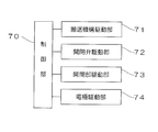
- FIG. 2 is a block diagram showing a control system of the film forming apparatus according to the present invention.
- the film forming apparatus includes a CPU that executes logical operations, a ROM that stores an operation program necessary for controlling the apparatus, a RAM that temporarily stores data during control, and the like, and a control unit that controls the entire apparatus. 70.
- the control unit 70 includes a conveyance mechanism driving unit 71 that controls the conveyance mechanism that moves the workpiece placement unit 13 illustrated in FIG. 1 and an on-off valve drive that controls opening and closing of the on-off valves 31, 34, 39, 48, and 49.
- a part 72, an opening / closing part driving part 73 that controls opening / closing of the opening / closing part 12, and an electrode driving part 74 that drives and controls the sputtering electrode 23 and the CVD electrode 24 are also connected.
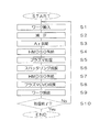
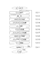
- FIG. 3 is a flowchart showing the film forming operation.
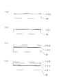
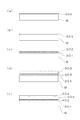
- FIG. 4 is a schematic diagram for explaining a film formation state on the workpiece W.
- the injection-molded work W is transferred from the injection molding machine and transferred into the film forming chamber 10 (step S1).
- the workpiece W placed on the workpiece placement unit 13 is moved to the CVD electrode 24 in the film forming chamber 10 as shown by a solid line in FIG. Arrange at the opposite position.
- the shutter 51 is disposed at a contact position that contacts the sputtering electrode 23 and covers the target material 22.
- the cylinder rod 54 of the air cylinder 53 is in a contracted state housed in the main body of the air cylinder 53.
- Step S2 the opening / closing part 12 is arranged at the closed position, and the inside of the film forming chamber 10 is depressurized from a low vacuum of about 0.1 Pascal to about 1 Pascal (Step S2).
- the depressurization is performed at a high speed to about 100 Pascal using an auxiliary pump 38 such as a rotary pump.
- the vacuum inside the film forming chamber 10 is about 0.1 to 1 Pascal in about 20 seconds. Can be depressurized.
- argon as an inert gas is supplied from the inert gas supply unit 33 into the film forming chamber 10, and the degree of vacuum in the film forming chamber 10 is 0.5-3.
- the inside of the film forming chamber 10 is filled with argon so as to be Pascal (step S3).
- An inert gas other than argon may be used, and depending on conditions, oxygen or nitrogen may be used instead of argon.
- HMDSO is supplied from the source gas supply unit 36 into the film forming chamber 10 (step S4).
- step S5 plasma processing is executed (step S5).
- a high frequency voltage of about 400 W is applied to the CVD electrode 24 from the high frequency power supply 45 via the matching box 46.
- HMDSO is supplied from the source gas supply unit 36 at a flow rate of about 5 sccm
- argon is supplied from the inert gas supply unit 33 at a flow rate of about 100 sccm.
- This plasma processing is completed in about several tens of seconds.
- a compound layer 100 made of Si, O, and C generated from HMDSO or the like is formed on the surface of the methacrylic resin workpiece W.
- step S6 sputtering film formation is performed (step S6).
- the work W placed on the work placement unit 13 is disposed at a position facing the sputtering electrode 23 in the film forming chamber 10.
- the shutter 51 is disposed at a retracted position near the bottom of the film forming chamber 10.
- Al collides with the compound layer 100 composed of Si, O, and C generated from HMDSO or the like by a sputtering phenomenon. And Si, O, and C are covalently bonded, or Al and Si, O, and C form a diffusion mixed layer, so that a mixed region 101 in which Al, Si, O, and C are mixed is formed.
- the thickness of the mixed region 101 is about several angstroms to several nanometers corresponding to several atomic layers.
- an Al thin film 102 is formed on the mixed region 101 as shown in FIG.
- the thickness of the Al thin film 102 is about 150 nanometers.
- a DC voltage is applied from the DC power supply 41 to the sputtering electrode 23 so that the input power is 25 watts per square centimeter or more with respect to the surface area of the target material 22 in the sputtering electrode 23. Is done. Thereby, even if the inside of the film formation chamber 10 is a low vacuum, the Al thin film 102 is suitably formed on the surface of the resin workpiece W.
- film formation by plasma CVD of Si oxide is subsequently performed.
- the work W placed on the work placement unit 13 is disposed at a position facing the CVD electrode 24 in the film formation chamber 10.
- the shutter 51 is disposed at a contact position that contacts the sputtering electrode 23 and covers the target material 22.
- Step S7 by opening the on-off valve 34, the source gas HMDSO is supplied from the source gas supply unit 36 into the film formation chamber 10, and the degree of vacuum in the film formation chamber 10 is 0.1 to 10 Pascals.
- step S8 film formation by plasma CVD is executed.
- the protective film 103 made of the source gas is deposited on the surface of the workpiece W (the surface of the Al thin film 102) by the plasma CVD reaction.
- Step S9 When the film formation by plasma CVD is completed, the inside of the film formation chamber 10 is vented. Then, after placing the opening / closing unit 12 at the loading / unloading position, the workpiece placing unit 13 is moved, and the workpiece W after completion of the deposition placed on the workpiece placing unit 13 is carried out of the deposition chamber 10. (Step S9).
- step S10 it is determined whether or not the processing for all the workpieces W has been completed.
- the apparatus is stopped.
- the process returns to step S1.
- step S5 when such a process is continuously performed, Si used in film formation by plasma CVD remains in the film formation chamber 10. Therefore, depending on the remaining amount of Si, the compound layer 100 composed of Si, O, and C may be formed in the plasma processing step (step S5) even when no additional Si is supplied. For this reason, it is possible to omit the HMDSO supply step in step S4.
- FIG. 5 shows a cross section of a region from the workpiece W to the Al thin film 102 shown in FIG. 4D when a film is formed by applying the film forming method according to the present invention.
- 6 to 8 are graphs showing the results of TEM-EDX (energy dispersive X-ray spectroscopy) analysis of points 1-1, 1-2, and 1-3 in FIG.
- FIG. 9 shows a cross section of a region from the workpiece W to the Al thin film 102 when a film is formed by applying a conventional film forming method, using a transmission electron microscope (TEM). It is a photograph.
- 10 to 12 are graphs showing the results of TEM-EDX (energy dispersive X-ray spectroscopy) analysis of the points 2-1, 2-2, and 2-3 in FIG.
- TEM-EDX energy dispersive X-ray spectroscopy
- the horizontal axis represents the energy of fluorescent X-rays
- the vertical axis represents the fluorescent X-ray intensity.
- the unit of fluorescent X-ray energy is keV (kilo electron volt).
- the fluorescent X-ray intensity indicates how much fluorescent X-ray having the energy is detected, and its unit is cps (Count Per Second).
- elemental analysis can be performed depending on where the peak of the fluorescent X-ray energy is detected. Note that the full-scale count values on the vertical axis in each figure are different from each other.
- the points 1-1 in FIG. 5 and the points 2-1 in FIG. 9 are both regions corresponding to the Al thin film 102 shown in FIG. In these points, Al is mainly detected, and there is no difference between the one to which the present invention shown in FIG. 5 is applied and the conventional one shown in FIG.
- the point 1-2 in FIG. 5 is an area corresponding to the mixed area 101 shown in FIG.
- a point 2-2 in FIG. 9 is an area corresponding to the boundary between the workpiece W and the Al thin film 102.
- Si is detected (see FIG. 7), but at point 2-2, Si is not detected (see FIG. 11).
- a point 1-3 in FIG. 5 and a point 2-3 in FIG. 9 are regions corresponding to the workpiece W, and components contained in the methacrylic resin are detected (see FIGS. 8 and 12).
- Al, Si, O, and C are present between the methacrylic resin work W and the Al thin film 102.
- Al and Si, O, and C are covalently bonded, or Al and Si, O, and C form a diffusion mixed layer.
- the action of the mixed region 101 can prevent embrittlement due to the cutting of the molecular chain on the surface of the methacrylic resin workpiece W, and the methacrylic resin workpiece W and the Al thin film 102 are firmly adhered to each other. It is possible to laminate in the state.
- FIG. 13 is a flowchart showing a film forming operation according to the second embodiment.
- FIG. 14 is a schematic diagram illustrating a film formation state on the workpiece W.
- the second embodiment is different from the above-described embodiment in that a Si oxide plasma CVD film forming step is provided between the plasma processing step and the sputtering film forming step.
- the description of the same steps as those in the above-described embodiment is simplified.
- the injection-molded work W is transferred from the injection molding machine and transferred into the film forming chamber 10 (step S11). Then, the inside of the film forming chamber 10 is depressurized from 0.1 Pascal to a low vacuum of about 1 Pascal (Step S12).
- step S13 argon as an inert gas is supplied from the inert gas supply unit 33 into the film forming chamber 10, and the degree of vacuum in the film forming chamber 10 is 0.5-3.
- the inside of the film forming chamber 10 is filled with argon so as to be Pascal (step S13).
- HMDSO is supplied from the source gas supply unit 36 into the film forming chamber 10 (step S14).
- plasma processing is executed (step S15).
- a high frequency voltage of about 400 W is applied to the CVD electrode 24 from the high frequency power supply 45 via the matching box 46.
- HMDSO is supplied from the source gas supply unit 36 at a flow rate of about 5 sccm
- argon is supplied from the inert gas supply unit 33 at a flow rate of about 100 sccm.
- This plasma processing is completed in about several tens of seconds.
- a mixed layer 200 of Si, O, and C generated from HMDSO or the like is formed on the surface of the methacrylic resin workpiece W.
- step S16 plasma CVD film formation of Si oxide is performed (step S16).
- the supply of argon is stopped, and HMDSO is supplied from the source gas supply unit 36 at a flow rate of about 60 sccm.
- a high frequency voltage of about 500 W is applied to the CVD electrode 24 from the high frequency power supply 45 through the matching box 46.
- This plasma CVD film forming process is completed in about 10 seconds.
- Si oxide film layer 201 is formed on the surface of the mixed layer 200.
- the thickness of the Si oxide film layer 201 is about several nanometers to 2 micrometers.
- step S17 sputtering film formation is executed (step S17).
- the work W placed on the work placement unit 13 is disposed at a position facing the sputtering electrode 23 in the film forming chamber 10.
- the shutter 51 is disposed at a retracted position near the bottom of the film forming chamber 10.
- Al collides with the Si oxide film layer 201 by a sputtering phenomenon, so that a part of the Si oxide film layer 201 is made of Al, Si, and O as shown in FIG. Are covalently bonded, or Al and Si and O form a diffusion mixed layer, so that a mixed region 202 in which Al and Si and O are mixed is formed.
- the thickness of the mixed region 202 is about several angstroms to several nanometers corresponding to several atomic layers.
- an Al thin film 203 is formed on the mixed region 202 as shown in FIG.
- the thickness of the Al thin film 203 is about 150 nanometers.
- a DC voltage is applied from the DC power source 41 to the sputtering electrode 23 so that the input power is 25 watts per square centimeter or more with respect to the surface area of the target material 22 in the sputtering electrode 23. Is done. Thereby, even if the inside of the film formation chamber 10 is a low vacuum, the Al thin film 203 is suitably formed on the surface of the resin workpiece W.
- film formation by plasma CVD of Si oxide is subsequently performed.
- the work W placed on the work placement unit 13 is disposed at a position facing the CVD electrode 24 in the film forming chamber 10.
- the shutter 51 is disposed at a contact position that contacts the sputtering electrode 23 and covers the target material 22.
- the source gas HMDSO is supplied from the source gas supply unit 36 into the film formation chamber 10, and the degree of vacuum in the film formation chamber 10 is 0.1 to 10 Pascals.
- a high frequency voltage is applied to the CVD electrode 24 from the high frequency power supply 45 through the matching box 46, thereby performing film formation by plasma CVD (step S19).
- the protective film 204 of the source gas is deposited on the surface of the workpiece W (the surface of the Al thin film 203) by the plasma CVD reaction.
- Step S20 When the film formation by plasma CVD is completed, the inside of the film formation chamber 10 is vented. Then, after placing the opening / closing unit 12 at the loading / unloading position, the workpiece placing unit 13 is moved, and the workpiece W after completion of the deposition placed on the workpiece placing unit 13 is carried out of the deposition chamber 10. (Step S20).
- step S21 it is determined whether or not the processing for all the workpieces W has been completed.
- the apparatus is stopped.
- the process returns to step S11.
- FIG. 15 is a flowchart showing a film forming operation according to the third embodiment.
- FIG. 16 is a schematic diagram for explaining a film formation state on the workpiece W.
- the plasma processing step and the Si oxide plasma CVD film forming step in the second embodiment described above are executed in reverse order. That is, when the thickness of the Si oxide film formed in the Si oxide plasma CVD film forming process is several tens of nanometers or less, the plasma processing process is performed after the Si oxide plasma CVD film forming process. Even if the configuration is adopted, the same effects as those of the second embodiment described above can be obtained.
- the injection-molded work W is transferred from the injection molding machine and transferred into the film forming chamber 10 (step S31). Then, the inside of the film forming chamber 10 is depressurized from 0.1 Pascal to a low vacuum of about 1 Pascal (Step S32).
- step S33 plasma CVD film formation of Si oxide is performed.
- HMDSO is supplied at a flow rate of about 60 sccm from the source gas supply unit 36 (step S33).
- a high frequency voltage of about 500 W is applied to the CVD electrode 24 from the high frequency power supply 45 through the matching box 46 (step S34).
- This plasma CVD film forming process is completed in about 10 seconds.
- Si oxide film layer 300 is formed on the surface of the methacrylic resin work W.
- the thickness of the Si oxide film layer 300 is several tens of nanometers or less.
- step S35 by opening the on-off valve 31, argon as an inert gas is supplied from the inert gas supply unit 33 into the film forming chamber 10, and the degree of vacuum in the film forming chamber 10 is 0.5-3.
- the inside of the film forming chamber 10 is filled with argon so as to be Pascal (step S35).
- step S36 plasma processing is executed (step S36).
- a high frequency voltage of about 400 W is applied to the CVD electrode 24 from the high frequency power supply 45 via the matching box 46.
- HMDSO is supplied from the source gas supply unit 36 at a flow rate of about 5 sccm
- argon is supplied from the inert gas supply unit 33 at a flow rate of about 100 sccm.
- This plasma processing is completed in about several tens of seconds.
- the Si oxide film layer 300 having a thickness of several tens of nanometers or less shown in FIG. 16A formed in the previous plasma CVD film forming step (step S34) disappears, and FIG. A mixed layer 301 of Si, O, and C is formed.
- step S37 sputtering film formation is executed (step S37).
- the work W placed on the work placement unit 13 is disposed at a position facing the sputtering electrode 23 in the film forming chamber 10.
- the shutter 51 is disposed at a retracted position near the bottom of the film forming chamber 10.
- Al collides with the mixed layer 301 of Si, O, and C by a sputtering phenomenon, so that a part of the mixed layer 301 of Si, O, and C is obtained as shown in FIG.
- the mixed region 302 in which Al and Si, C, and O are mixed Al or Si, C, and O are covalently bonded, or Al and Si, C, and O form a diffusion mixed layer.
- the thickness of the mixed region 302 is about several angstroms to several nanometers corresponding to several atomic layers.
- an Al thin film 303 is formed on the mixed region 302 as shown in FIG.
- the thickness of the Al thin film 303 is about 150 nanometers.
- a DC voltage is applied from the DC power source 41 to the sputtering electrode 23 so that the input power is 25 watts per square centimeter or more with respect to the surface area of the target material 22 in the sputtering electrode 23. Is done. Thereby, even if the inside of the film formation chamber 10 is a low vacuum, the Al thin film 303 is suitably formed on the surface of the resin workpiece W.
- film formation by plasma CVD of Si oxide is subsequently performed.
- the work W placed on the work placement unit 13 is disposed at a position facing the CVD electrode 24 in the film forming chamber 10.
- the shutter 51 is disposed at a contact position that contacts the sputtering electrode 23 and covers the target material 22.
- the source gas HMDSO is supplied from the source gas supply unit 36 into the film formation chamber 10, and the degree of vacuum in the film formation chamber 10 is 0.1 to 10 Pascals.
- a high-frequency voltage is applied to the CVD electrode 24 from the high-frequency power supply 45 through the matching box 46, thereby forming a film of Si oxide by plasma CVD (step S39).
- the protective film 304 made of the source gas is deposited on the surface of the workpiece W (the surface of the Al thin film 303) by the plasma CVD reaction.
- Step S40 When film formation by plasma CVD of Si oxide is completed, the film formation chamber 10 is vented. Then, after placing the opening / closing unit 12 at the loading / unloading position, the workpiece placing unit 13 is moved, and the workpiece W after completion of the deposition placed on the workpiece placing unit 13 is carried out of the deposition chamber 10. (Step S40).
- step S41 it is determined whether or not the processing for all the workpieces W has been completed.
- the apparatus is stopped.
- the process returns to step S11.
- FIG. 17 is a schematic view of a film forming apparatus for executing a film forming method according to the fourth embodiment of the present invention.
- the same members as those in the film forming apparatus shown in FIG. 1 are denoted by the same reference numerals, and detailed description thereof is omitted.
- a film forming apparatus for carrying out the film forming method according to the fourth embodiment has an on-off valve 81, a flow rate adjusting valve 82, and a film forming apparatus shown in FIG.
- an oxygen supply unit 83 is added.
- the film forming method according to the first embodiment when the supply amount of HMDSO is excessive or depending on the contamination inside the apparatus, undecomposed HMDSO is recombined and deposited on the surface of the methacrylic resin. In some cases, the surface roughness increases and the regular reflectance decreases from before the treatment. For this reason, in the film forming method according to the fourth embodiment, the gas type is changed from argon to oxygen.
- the plasma treatment removes moisture adhering to the surface of the methacrylic resin during rapid evacuation, reduces the oxidation of the sputtered film during subsequent processing, and improves the reflectance.
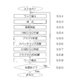
- FIG. 18 is a flowchart showing the film forming operation according to the fourth embodiment of the present invention. In the following, the description of the same steps as the film forming operation according to the first embodiment described above is simplified.
- the injection-molded work W is transferred from the injection molding machine and transferred into the film forming chamber 10 (step S51).
- the inside of the film forming chamber 10 is depressurized from 0.1 Pascal to a low vacuum of about 1 Pascal (Step S52).
- step S53 oxygen is supplied from the oxygen supply unit 83 into the film formation chamber 10, so that the degree of vacuum in the film formation chamber 10 is 0.5 to 3 Pascals.
- step S53 oxygen is supplied from the oxygen supply unit 83 into the film formation chamber 10.
- step S54 HMDSO is supplied from the source gas supply unit 36 into the film forming chamber 10.
- plasma processing is executed (step S55).
- a high frequency voltage of about 400 W is applied to the CVD electrode 24 from the high frequency power supply 45 via the matching box 46.
- HMDSO is supplied from the source gas supply unit 36 at a flow rate of about 5 sccm, and oxygen is supplied from the oxygen supply unit 83 at a flow rate of about 100 sccm.
- This plasma processing is completed in about several tens of seconds.
- step S56 sputtering film formation is executed.
- film formation by sputtering is completed, film formation by plasma CVD of Si oxide is subsequently performed.
- HMDSO which is a raw material gas is supplied into the film forming chamber 10, and the degree of vacuum in the film forming chamber 10 is set to 0.1 to 10 pascals (step S57).
- a high frequency voltage is applied to the CVD electrode 24 to perform film formation by plasma CVD (step S58).
- step S59 It is determined whether or not the processing for all the workpieces W has been completed (step S10).
- the apparatus is stopped. On the other hand, when there is an unprocessed work W, the process returns to step S51.
- oxygen is supplied instead of supplying argon in steps S3 to S5 in the film forming method according to the first embodiment.
- steps S13 to S15 in the film forming method according to the second embodiment oxygen may be supplied instead of supplying argon.
- oxygen may be supplied in the film forming method according to the third embodiment.
- steps S35 to S36 oxygen may be supplied instead of supplying argon.
- the present invention is applied to a film forming apparatus that continuously performs film formation by sputtering and film formation by plasma CVD in the same film formation chamber 10 will be described.
- the present invention may be applied to a film forming apparatus that executes only film formation by sputtering.
Landscapes
- Chemical & Material Sciences (AREA)
- Engineering & Computer Science (AREA)
- Mechanical Engineering (AREA)
- Organic Chemistry (AREA)
- Metallurgy (AREA)
- Materials Engineering (AREA)
- Chemical Kinetics & Catalysis (AREA)
- Physics & Mathematics (AREA)
- General Chemical & Material Sciences (AREA)
- Plasma & Fusion (AREA)
- Optics & Photonics (AREA)
- General Physics & Mathematics (AREA)
- Inorganic Chemistry (AREA)
- Laminated Bodies (AREA)
- Physical Vapour Deposition (AREA)
- Chemical Vapour Deposition (AREA)
Abstract
Description
11 本体
12 開閉部
13 ワーク載置部
19 接地部
21 電極部
22 ターゲット材料
23 スパッタ電極
24 CVD電極
31 開閉弁
32 流量調整弁
33 不活性ガスの供給部
34 開閉弁
35 流量調整弁
36 原料ガスの供給源
37 ターボ分子ポンプ
38 補助ポンプ
39 開閉弁
41 直流電源
45 高周波電源
46 マッチングボックス
48 開閉弁
49 開閉弁
51 シャッター
70 制御部
71 搬送機構駆動部
72 開閉弁駆動部
73 開閉部駆動部
74 電極駆動部
81 開閉弁
82 流量調整弁
83 酸素の供給部
100 化合物層
101 混在領域
102 Alの薄膜
103 保護膜
200 混在層
201 Si酸化膜層
202 混在領域
203 Alの薄膜
204 保護膜
300 Si酸化膜層
301 混在層
302 混在領域
303 Alの薄膜
304 保護膜
W ワーク
Claims (16)
- 樹脂と金属薄膜とが積層された構造体であって、
前記樹脂と前記金属薄膜との間に、前記金属薄膜を構成する原子とSiとが混在する混在領域を有することを特徴とする構造体。 - 請求項1に記載の構造体において、前記混在領域には、前記金属薄膜を構成する原子およびSiとともに、OまたはCのうちの少なくとも一つが混在する構造体。
- 請求項1に記載の構造体において、
前記樹脂は、メタクリル樹脂である構造体。 - 請求項1に記載の構造体において、
前記金属薄膜は、スパッタリング法により形成される構造体。 - 請求項4に記載の構造体において、
前記金属薄膜は、AlまたはAlを主成分とする金属で構成される構造体。 - 請求項5に記載の構造体において、
Si存在下でプラズマ処理を実行した後、スパッタリング法により前記金属薄膜を形成するときに、AlとSiとが混在する混在領域が形成される構造体。 - 請求項1から請求項6のいずれかに記載の構造体において、
前記混在領域は、前記金属薄膜を構成する原子が、Si、O、Cのいずれかと共有結合し、あるいは、前記金属薄膜を構成する原子が、Si、O、Cのいずれかと拡散混合層を形成する構造体。 - 請求項1から請求項6のいずれかに記載の構造体において、
前記樹脂と前記金属薄膜との間に、SiとOとCとの混在層と、Si酸化物を含む化合物層と、前記金属薄膜を構成する原子とSiとOとの混在層とがこの順に積層される構造体。 - 請求項1から請求項6のいずれかに記載の構造体において、
前記樹脂と前記金属薄膜との間に、SiとOとCとの混在層と、前記金属薄膜を構成する原子とSiとOとの混在層とがこの順に積層される構造体。 - 請求項1から請求項6のいずれかに記載の構造体において、
前記金属薄膜の表面に、さらに、保護膜が形成される構造体。 - 請求項10に記載の構造体において、
前記保護膜は、Si酸化物系保護膜である構造体。 - 樹脂製のワークに対して金属薄膜を成膜する成膜方法であって、
樹脂製のワークに対してSiの存在下でプラズマ処理を実行するプラズマ処理工程と、
前記ワークに対して金属製のターゲット材料によりスパッタリング成膜を実行するスパッタリング成膜工程と、
を含むことを特徴とする成膜方法。 - 請求項12に記載の成膜方法において、
チャンバー内に前記ワークを搬入するワーク搬入工程と、
チャンバー内にSiを含む不活性ガスを供給する不活性ガス供給工程と、
プラズマCVDによりSiを含む膜を成膜するCVD工程と、
スパッタリングにより金属薄膜を成膜するスパッタリング成膜工程と、
を含む成膜方法。 - 請求項12に記載の成膜方法において、
チャンバー内に前記ワークを搬入するワーク搬入工程と、
チャンバー内にSiを含む酸素を供給する酸素供給工程と、
プラズマCVDによりSiを含む膜を成膜するCVD工程と、
スパッタリングにより金属薄膜を成膜するスパッタリング成膜工程と、
を含む成膜方法。 - 請求項12に記載の成膜方法において、
前記プラズマ処理工程の前、または、前記プラズマ処理工程と前記スパッタリング成膜工程との間に、Si酸化物のプラズマCVD成膜工程を有する成膜方法。 - 請求項12から請求項14のいずれかに記載の成膜方法において、
前記スパッタリング成膜工程の後に、
前記チャンバー内に原料ガスを供給する原料ガス供給工程と、
プラズマCVDにより原料ガスを含む膜を成膜する工程と、
を含む成膜方法
Priority Applications (3)
| Application Number | Priority Date | Filing Date | Title |
|---|---|---|---|
| CN201580006176.0A CN105939847B (zh) | 2014-01-30 | 2015-01-20 | 构造体及成膜方法 |
| JP2015559878A JP6361665B2 (ja) | 2014-01-30 | 2015-01-20 | 構造体および成膜方法 |
| US15/115,563 US20170067142A1 (en) | 2014-01-30 | 2015-01-20 | Structure and film formation method |
Applications Claiming Priority (4)
| Application Number | Priority Date | Filing Date | Title |
|---|---|---|---|
| JP2014015150 | 2014-01-30 | ||
| JP2014-015150 | 2014-01-30 | ||
| JP2014-123445 | 2014-06-16 | ||
| JP2014123445 | 2014-06-16 |
Publications (1)
| Publication Number | Publication Date |
|---|---|
| WO2015115249A1 true WO2015115249A1 (ja) | 2015-08-06 |
Family
ID=53756826
Family Applications (1)
| Application Number | Title | Priority Date | Filing Date |
|---|---|---|---|
| PCT/JP2015/051373 Ceased WO2015115249A1 (ja) | 2014-01-30 | 2015-01-20 | 構造体および成膜方法 |
Country Status (4)
| Country | Link |
|---|---|
| US (1) | US20170067142A1 (ja) |
| JP (1) | JP6361665B2 (ja) |
| CN (1) | CN105939847B (ja) |
| WO (1) | WO2015115249A1 (ja) |
Cited By (2)
| Publication number | Priority date | Publication date | Assignee | Title |
|---|---|---|---|---|
| CN106480402A (zh) * | 2015-08-26 | 2017-03-08 | 株式会社岛津制作所 | 成膜装置及成膜方法 |
| JP2017082291A (ja) * | 2015-10-29 | 2017-05-18 | 株式会社島津製作所 | 成膜方法および成膜装置 |
Families Citing this family (1)
| Publication number | Priority date | Publication date | Assignee | Title |
|---|---|---|---|---|
| US20230304139A1 (en) * | 2022-03-25 | 2023-09-28 | Vergason Technology, Inc. | Methods for applying decorative metal films on polymeric surfaces |
Citations (11)
| Publication number | Priority date | Publication date | Assignee | Title |
|---|---|---|---|---|
| JPH0886908A (ja) * | 1994-09-16 | 1996-04-02 | Ricoh Co Ltd | 光学部品の製造方法及び光学部品の製造装置 |
| JPH08192492A (ja) * | 1995-01-17 | 1996-07-30 | Mitsui Toatsu Chem Inc | 透明導電性フィルム |
| JPH08304614A (ja) * | 1995-05-12 | 1996-11-22 | Ricoh Co Ltd | 合成樹脂製反射鏡、その製造方法および製造装置 |
| JP2001116912A (ja) * | 1999-10-21 | 2001-04-27 | Oike Ind Co Ltd | 半透過半反射拡散フイルム |
| JP2002248355A (ja) * | 2001-02-27 | 2002-09-03 | Ulvac Japan Ltd | 光触媒装置 |
| JP2008504994A (ja) * | 2004-07-02 | 2008-02-21 | レーアウ アクチエンゲゼルシヤフト ウント コンパニー | ポリマーのための多重層の層構造体 |
| WO2008133136A1 (ja) * | 2007-04-16 | 2008-11-06 | Konica Minolta Opto, Inc. | 反射鏡 |
| JP2009107333A (ja) * | 2007-10-12 | 2009-05-21 | Hitachi Chem Co Ltd | 導電性回路付き透明樹脂積層体及びその製造方法 |
| JP2010058111A (ja) * | 2008-08-06 | 2010-03-18 | 憲一 ▲高▼木 | コーティング方法及び該コーティング方法で表面処理したプラスティック製品 |
| JP2011203725A (ja) * | 2003-08-07 | 2011-10-13 | Sabic Innovative Plastics Ip Bv | 反射性物品及びその製造方法 |
| JP2013226718A (ja) * | 2012-04-26 | 2013-11-07 | Kojima Press Industry Co Ltd | 樹脂製品及びその製造方法 |
Family Cites Families (8)
| Publication number | Priority date | Publication date | Assignee | Title |
|---|---|---|---|---|
| JP2787987B2 (ja) * | 1989-11-22 | 1998-08-20 | 株式会社リコー | 反射鏡 |
| JPH04235502A (ja) * | 1991-01-10 | 1992-08-24 | Nisshin Koki Kk | 反射鏡 |
| JPH055801A (ja) * | 1991-06-27 | 1993-01-14 | Central Glass Co Ltd | 樹脂製鏡 |
| CZ281073B6 (cs) * | 1993-09-03 | 1996-06-12 | Fyzikální ústav AVČR | Způsob rozprašování materiálu katody |
| US6110544A (en) * | 1997-06-26 | 2000-08-29 | General Electric Company | Protective coating by high rate arc plasma deposition |
| JP2002228815A (ja) * | 2001-02-06 | 2002-08-14 | Yuka Denshi Co Ltd | 投射ミラー |
| JP2005004892A (ja) * | 2003-06-12 | 2005-01-06 | Sony Corp | 磁気記録媒体および磁気記録媒体の製造方法 |
| US20140295141A1 (en) * | 2013-03-27 | 2014-10-02 | E I Du Pont De Nemours And Company | Making the Surface of an Article Visibly Line Free |
-
2015
- 2015-01-20 US US15/115,563 patent/US20170067142A1/en not_active Abandoned
- 2015-01-20 CN CN201580006176.0A patent/CN105939847B/zh active Active
- 2015-01-20 WO PCT/JP2015/051373 patent/WO2015115249A1/ja not_active Ceased
- 2015-01-20 JP JP2015559878A patent/JP6361665B2/ja active Active
Patent Citations (11)
| Publication number | Priority date | Publication date | Assignee | Title |
|---|---|---|---|---|
| JPH0886908A (ja) * | 1994-09-16 | 1996-04-02 | Ricoh Co Ltd | 光学部品の製造方法及び光学部品の製造装置 |
| JPH08192492A (ja) * | 1995-01-17 | 1996-07-30 | Mitsui Toatsu Chem Inc | 透明導電性フィルム |
| JPH08304614A (ja) * | 1995-05-12 | 1996-11-22 | Ricoh Co Ltd | 合成樹脂製反射鏡、その製造方法および製造装置 |
| JP2001116912A (ja) * | 1999-10-21 | 2001-04-27 | Oike Ind Co Ltd | 半透過半反射拡散フイルム |
| JP2002248355A (ja) * | 2001-02-27 | 2002-09-03 | Ulvac Japan Ltd | 光触媒装置 |
| JP2011203725A (ja) * | 2003-08-07 | 2011-10-13 | Sabic Innovative Plastics Ip Bv | 反射性物品及びその製造方法 |
| JP2008504994A (ja) * | 2004-07-02 | 2008-02-21 | レーアウ アクチエンゲゼルシヤフト ウント コンパニー | ポリマーのための多重層の層構造体 |
| WO2008133136A1 (ja) * | 2007-04-16 | 2008-11-06 | Konica Minolta Opto, Inc. | 反射鏡 |
| JP2009107333A (ja) * | 2007-10-12 | 2009-05-21 | Hitachi Chem Co Ltd | 導電性回路付き透明樹脂積層体及びその製造方法 |
| JP2010058111A (ja) * | 2008-08-06 | 2010-03-18 | 憲一 ▲高▼木 | コーティング方法及び該コーティング方法で表面処理したプラスティック製品 |
| JP2013226718A (ja) * | 2012-04-26 | 2013-11-07 | Kojima Press Industry Co Ltd | 樹脂製品及びその製造方法 |
Cited By (2)
| Publication number | Priority date | Publication date | Assignee | Title |
|---|---|---|---|---|
| CN106480402A (zh) * | 2015-08-26 | 2017-03-08 | 株式会社岛津制作所 | 成膜装置及成膜方法 |
| JP2017082291A (ja) * | 2015-10-29 | 2017-05-18 | 株式会社島津製作所 | 成膜方法および成膜装置 |
Also Published As
| Publication number | Publication date |
|---|---|
| CN105939847B (zh) | 2018-09-04 |
| US20170067142A1 (en) | 2017-03-09 |
| JP6361665B2 (ja) | 2018-07-25 |
| CN105939847A (zh) | 2016-09-14 |
| JPWO2015115249A1 (ja) | 2017-03-23 |
Similar Documents
| Publication | Publication Date | Title |
|---|---|---|
| Mohagheghpour et al. | Correlation study of structural, optical and electrical properties of amorphous carbon thin films prepared by ion beam sputtering deposition technique | |
| JP2002511115A (ja) | スパッタリングのバーンインに要する時間を短縮してスパッタリングの際に発生するパーティクルを最小限に抑える方法、及びこのときに用いられるターゲットアセンブリ | |
| JP6093362B2 (ja) | 基板上に反射低減層を生成するための方法および装置 | |
| JP6361665B2 (ja) | 構造体および成膜方法 | |
| JP6814633B2 (ja) | 薄型基板およびその製造方法、並びに基板の搬送方法 | |
| WO2022241952A1 (zh) | 一种纳米多层结构过渡金属氮化物涂层及其制备方法和应用 | |
| KR20160058816A (ko) | 기판 본딩 장치 및 방법 | |
| JP6555078B2 (ja) | 成膜方法 | |
| JP6202098B2 (ja) | 成膜装置および成膜方法 | |
| CN111926293A (zh) | 光学器件及其制造方法 | |
| JP4768679B2 (ja) | 酸化亜鉛膜の形成方法 | |
| US20120276407A1 (en) | Process for surface treating iron-based alloy and article | |
| JP2015101768A (ja) | 成膜装置 | |
| JP6477221B2 (ja) | 成膜方法 | |
| US9719164B2 (en) | Method of manufacturing compound film | |
| JP2017043803A (ja) | 成膜装置および成膜方法 | |
| Ong et al. | Strong photoluminescence with fine structures from sandwich-structured films of silicon nanoparticles embedded in Al2O3 matrices | |
| JP4895897B2 (ja) | 薄膜構造体及びその製造方法 | |
| JP2015113513A (ja) | 成膜装置および成膜方法 | |
| JP3506782B2 (ja) | 光学薄膜の製造方法 | |
| CN103233199B (zh) | 一种提高基材表面氮化物硬质涂层光亮度及硬度的方法 | |
| JP4863494B2 (ja) | 微細構造観察用試料の作製方法 | |
| JP7188281B2 (ja) | 成膜方法、樹脂製品の製造方法および成膜装置 | |
| JP2015151618A (ja) | 成膜装置 | |
| Zhou et al. | Thermally Stable Multilayer Coating with a Diffusion Barrier for Interference Colors |
Legal Events
| Date | Code | Title | Description |
|---|---|---|---|
| 121 | Ep: the epo has been informed by wipo that ep was designated in this application |
Ref document number: 15742872 Country of ref document: EP Kind code of ref document: A1 |
|
| ENP | Entry into the national phase |
Ref document number: 2015559878 Country of ref document: JP Kind code of ref document: A |
|
| WWE | Wipo information: entry into national phase |
Ref document number: 15115563 Country of ref document: US |
|
| NENP | Non-entry into the national phase |
Ref country code: DE |
|
| 122 | Ep: pct application non-entry in european phase |
Ref document number: 15742872 Country of ref document: EP Kind code of ref document: A1 |