WO2015111489A1 - 有機エレクトロルミネッセンス素子 - Google Patents
有機エレクトロルミネッセンス素子 Download PDFInfo
- Publication number
- WO2015111489A1 WO2015111489A1 PCT/JP2015/050885 JP2015050885W WO2015111489A1 WO 2015111489 A1 WO2015111489 A1 WO 2015111489A1 JP 2015050885 W JP2015050885 W JP 2015050885W WO 2015111489 A1 WO2015111489 A1 WO 2015111489A1
- Authority
- WO
- WIPO (PCT)
- Prior art keywords
- group
- layer
- ring
- organic
- region
- Prior art date
Links
Images

Classifications
-
- H—ELECTRICITY
- H10—SEMICONDUCTOR DEVICES; ELECTRIC SOLID-STATE DEVICES NOT OTHERWISE PROVIDED FOR
- H10K—ORGANIC ELECTRIC SOLID-STATE DEVICES
- H10K59/00—Integrated devices, or assemblies of multiple devices, comprising at least one organic light-emitting element covered by group H10K50/00
- H10K59/10—OLED displays
- H10K59/221—Static displays, e.g. displaying permanent logos
-
- H—ELECTRICITY
- H10—SEMICONDUCTOR DEVICES; ELECTRIC SOLID-STATE DEVICES NOT OTHERWISE PROVIDED FOR
- H10K—ORGANIC ELECTRIC SOLID-STATE DEVICES
- H10K50/00—Organic light-emitting devices
- H10K50/10—OLEDs or polymer light-emitting diodes [PLED]
- H10K50/14—Carrier transporting layers
- H10K50/15—Hole transporting layers
- H10K50/156—Hole transporting layers comprising a multilayered structure
Definitions
- the present invention relates to an organic electroluminescence element.
- the present invention relates to an organic electroluminescence element that has a light emission pattern of a predetermined shape and can suppress a decrease in light emission luminance of a light emitting region even when driven for a long time.
- organic electroluminescence elements (hereinafter also referred to as “organic EL elements”) have been actively developed and used as display devices and illumination devices.
- An organic EL element is a thin-film type solid-state element that can emit light at a low voltage of several volts to several tens of volts, and has many excellent features such as high brightness, high luminous efficiency, thinness, and light weight.
- An organic EL element is configured by sandwiching an organic functional layer made of an organic material between a pair of electrodes, and emitted light generated in the organic functional layer passes through the electrode and is extracted outside.
- the organic functional layer laminated on the glass substrate is irradiated with ultraviolet rays, and the irradiated portion is deteriorated to form a non-light emitting region, and the organic EL element has a predetermined shape.
- a technique for providing a light emission pattern is proposed (see, for example, Patent Document 1).
- this technique has a problem that it is sometimes difficult to control the amount of ultraviolet irradiation, for example, the resin base material may turn yellow due to ultraviolet irradiation.
- the organic EL element having the light emission pattern of the predetermined shape is obtained.
- the luminance of the light emitting region may decrease.
- the present invention has been made in view of the above problems and situations, and a solution to the problem is organic electroluminescence that has a light emission pattern of a predetermined shape and can suppress a decrease in light emission luminance of a light emitting region even when driven for a long time. It is to provide an element.
- an organic electroluminescence device having an organic functional layer including at least a hole transport layer and a light-emitting layer between an anode and a cathode.
- any one of the organic functional layers is formed as a design pattern display control unit, and the design pattern display control unit includes a region where current flows when the organic EL element is driven and a region where current is less likely to flow than the region.
- An organic electroluminescence device having an organic functional layer including at least a hole transport layer and a light emitting layer between an anode and a cathode, Any one of the organic functional layers is formed as a design pattern display control unit, and the design pattern display control unit includes a region where current flows when the organic electroluminescence element is driven, and a region where current is less likely to flow than the region.
- the organic electroluminescent element characterized by displaying an appropriate design pattern as the said organic electroluminescent element whole by comprising.
- control of the amount of current in the region where the current flows and the region where the current does not easily flow is included in the design pattern display control unit is controlled by a hole injection amount. element.
- organic functional layer according to item 1 or 2 wherein the organic functional layer formed as the design pattern display control unit is at least one of a hole injection layer and a hole transport layer. Electroluminescence element.
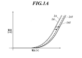
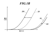
- FIG. 1A shows current-voltage characteristics 1A, 1A1 in the light-emitting region of the organic EL element of the present invention, and current-voltage characteristics 2A, 2A1 in the light-emitting area of the conventional organic EL element, and FIG.
- a conventional organic EL device having a light-emitting pattern with a predetermined shape by ultraviolet irradiation is the light-emitting pattern when the driving voltage of the device is increased by irradiating ultraviolet rays to at least one of the organic functional layers including the light-emitting layer.
- the current-voltage characteristic 1A of the light-emitting region and the current-voltage characteristic 2B of the non-light-emitting region are approximated and are driven for a long time.
- the current-voltage characteristic 2B1 in the non-light emitting region may shift to the current-voltage characteristic 2A1 side in the light emitting region.
- the current characteristics of the non-light-emitting region are more likely to flow than in the initial stage, and the luminance of the light-emitting region is changed by changing the feeding current to the light-emitting region. It may decrease.
- any one of the organic functional layers is configured by forming an organic layer configuration in which a region where current flows when driving and a region where current is less likely to flow than the region, so that a region where current flows can be obtained.
- a light emitting region is formed, and a region where current is difficult to flow forms a non-light emitting region.
- the current-voltage characteristics 1A and 1B of both are not approximate, and even if the current-voltage characteristics 1A and 1B shift by driving for a long time,
- the current-voltage characteristic 1B1 in the light emitting region is less likely to shift to the lower voltage side than the current-voltage characteristic 1A1 in the light emitting region.
- the organic electroluminescent element of the present invention is an element having an organic functional layer including at least a hole transport layer and a light emitting layer between an anode and a cathode, and any one of the organic functional layers is a design pattern display control unit.
- the design pattern display control unit is composed of a region through which current flows when the organic electroluminescence device is driven and a region through which current is less likely to flow than the region, thereby the organic electroluminescence device. As a whole, an appropriate design pattern is displayed. This feature is a technical feature common to the inventions according to claims 1 to 5.
- control of the current amount in the region where the current flows and the region where the current hardly flows is included in the design pattern display control unit is controlled by the hole injection amount.
- the organic functional layer formed as the said design pattern display control part is at least any one layer of a positive hole injection layer and the said positive hole transport layer.
- the anode is preferably a thin film electrode mainly composed of silver.
- the display of the design pattern can be controlled by the light emission start voltage.
- the light emitting layer according to the present invention is composed of a single layer or a plurality of layers, and when there are a plurality of light emitting layers, a non-light emitting intermediate layer may be provided between the light emitting layers.
- a hole blocking layer also referred to as a hole blocking layer
- an electron injection layer also referred to as a cathode buffer layer
- An electron blocking layer also referred to as an electron barrier layer
- a hole injection layer also referred to as an anode buffer layer
- the electron transport layer according to the present invention is a layer having a function of transporting electrons, and in a broad sense, an electron injection layer and a hole blocking layer are also included in the electron transport layer and may be composed of a plurality of layers.
- the hole transport layer according to the present invention is a layer having a function of transporting holes, and in a broad sense, a hole injection layer and an electron blocking layer are also included in the hole transport layer, and are composed of a plurality of layers. Also good.
- the hole transport layer in a narrow sense may be composed of a plurality of layers.
- the layer excluding the anode and the cathode is referred to as “organic functional layer”.
- the organic EL element according to the present invention may be a so-called tandem structure element including at least one light-emitting layer and a plurality of light-emitting units composed of any one of the organic functional layers. good.
- the plurality of light emitting units may all be the same or different. Further, the two light emitting units may be the same, and the remaining one may be different.
- the plurality of light emitting units may be laminated directly or via an intermediate layer (also called an intermediate electrode, an intermediate conductive layer, a charge generation layer, an electron extraction layer, a connection layer, or an intermediate insulating layer).
- An intermediate layer also called an intermediate electrode, an intermediate conductive layer, a charge generation layer, an electron extraction layer, a connection layer, or an intermediate insulating layer.
- a known material structure can be used as long as a layer having a function of supplying electrons to the adjacent layer on the side is provided and a layer having a function of supplying holes to the adjacent layer on the cathode side is provided.
- Examples of materials used for the intermediate layer include ITO (indium tin oxide), IZO (indium zinc oxide), ZnO 2 , TiN, ZrN, HfN, TiOx, VOx, CuI, InN, GaN, and CuAlO 2. , CuGaO 2 , SrCu 2 O 2 , LaB 6 , RuO 2 , Al, etc., conductive inorganic compound layers, bilayer films and multilayer films of these conductive inorganic compounds, fullerenes such as C60, and conductivity such as oligothiophene Examples include organic material layers, conductive organic compound layers such as metal phthalocyanines, metal-free phthalocyanines, and porphyrins, but the present invention is not limited thereto.
- Preferred examples of the structure within the light emitting unit include those obtained by removing the anode and the cathode from the structures (1) to (7) mentioned in the above representative element structures, but the present invention is not limited to these. Not.
- tandem organic EL element examples include, for example, US Pat. No. 7,420,203, US Pat. No. 7,473,923, US Pat. No. 6,872,472, US Pat. No. 6,107,734, US Pat. No. 6,337,492, and JP 2011-96679A.
- the present invention is not limited to these.
- the organic EL element of the present invention includes a design pattern display control unit, and thus can emit light with a light emission pattern having a predetermined shape.
- the “design pattern” refers to a design (design or pattern in the figure), characters, images, etc. displayed by the organic EL element.
- “Patterning” or “patterning” means providing these pattern display functions.
- the “light emission pattern” of an organic EL element means that when the organic EL element emits light, the light emission intensity (luminance) is determined by the position of the light emitting surface based on a predetermined design (pattern or pattern in the figure), characters, images, etc.
- the design pattern display control unit is a layer in which any one of the organic functional layers constituting the organic EL element of the present invention is patterned using an evaporation mask, and a current flows when the organic EL element is driven. And a region where current is less likely to flow than that region.
- a region where current flows constitutes a light emitting region, and a region where current hardly flows constitutes a non-light emitting region, whereby the organic EL element of the present invention has an appropriate design pattern as the whole organic EL element.
- the region where current does not easily flow refers to a region having a current-voltage characteristic on the high voltage side of +2 V or more of the current-voltage characteristic of the region where the current flows.
- the control of the amount of current in the region where the current flows and the region where the current is less likely to flow than the region is preferably performed by controlling the hole injection amount.
- the organic EL element is formed using a hole injection layer / first hole transport layer / second hole transport layer / blue light emitting layer / green light emitting layer /
- the hole injection amount can be controlled by patterning the hole injection layer and the first hole transport layer. That is, in the region where each organic functional layer overlaps, the place where the hole injection layer and the first hole transport layer are not formed is the place where the hole injection layer and the first hole transport layer are formed.
- the amount of hole injection is smaller than that, the light emission starting voltage is increased. As a result, current easily flows in the locations where the hole injection layer and the first hole transport layer are formed, and current does not easily flow in locations where the hole injection layer and the first hole transport layer are not formed. Yes.
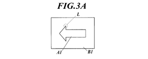
- the region where current is difficult to flow has an increased light emission start voltage as described above, but is not in a completely insulated state. Therefore, even when the light emission pattern having a predetermined shape includes a sharp shape, that is, when the region where the current easily flows in the design pattern display control unit includes a sharp shape in plan view, the organic EL element is driven. The current is not concentrated locally, and the occurrence of a short circuit can be suppressed. Specifically, for example, in a conventional organic EL element having a light emission pattern composed of a light emission region A1 and a non-light emission region B1 as shown in FIG. 3A, the non-light emission region B1 is in an electrically insulated state.
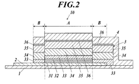
- the organic EL element 10 provided with a design pattern display control unit will be described with reference to FIG.
- the organic EL element 10 is configured by laminating an anode 2, an organic functional layer 3, a cathode 4, and the like on a substrate 1.
- the organic functional layer 3 includes a hole injection layer 31, a first hole transport layer 32, a second hole transport layer 33, a light emitting layer 34, an electron transport layer 35, and an electron injection layer 36.
- the hole injection layer 31 and the first hole transporting layer of the organic functional layer 3 are laminated.
- the hole injection layer 31 and the first hole transport layer 32 are patterned layers, and these layers constitute a design pattern display control unit.
- the amount of hole injection in the region B can be made smaller than the amount of hole injection in the region A
- the region B is a region where current does not easily flow (non-light emitting region)
- the region A is a region where current flows (light emission).
- the region B is not in a completely insulated state and a minute current flows, it is possible to suppress the current from being concentrated on the edge portion of the region A and the like, thereby suppressing the occurrence of a short circuit.
- the design pattern display control unit is configured by patterning the hole injection layer 31 and the first hole transport layer 32.
- the design pattern display control unit may be configured by patterning another organic functional layer as long as a region where current is less likely to flow can be formed.
- each light emitting unit may be provided with a design pattern display control unit, and the design pattern display control unit may be configured to emit light with different light emission patterns. good.
- the organic EL device of the present invention configured as shown in FIG. 2 has the same layer structure as that of FIG. 2, and includes a hole injection layer, a first hole transport layer, a second hole transport layer, and light emission.
- a current-voltage characteristic of a conventional organic EL element in which a light emitting pattern is provided by patterning a layer will be described with reference to FIGS. 1A and 1B.
- FIG. 1A shows current-voltage characteristics 1A, 1A1 in the light-emitting region of the organic EL element of the present invention, and current-voltage characteristics 2A, 2A1 in the light-emitting area of the conventional organic EL element
- FIG. 1B shows the organic-voltage characteristics of the present invention.
- the current-voltage characteristics 1B and 1B1 in the non-light-emitting region of the EL element and the current-voltage characteristics 2B and 2B1 in the non-light-emitting region of the conventional organic EL element are shown.
- the current-voltage characteristics 1A1, 1B1, 2A1, and 2B1 indicate the current-voltage characteristics after each organic EL element is driven for a long time.
- the conventional organic EL element can emit light with the light emission pattern by forming a light emitting layer or the like in the organic functional layer in a predetermined pattern shape.
- the current-voltage characteristic 2A in the light-emitting region and the current-voltage characteristic 2B in the non-light-emitting region are approximated, and the current voltage in the non-light-emitting region is obtained by being driven for a long time.
- the characteristic 2B1 may shift to a lower voltage side than the current-voltage characteristic 2A1 of the light emitting region. For this reason, in the conventional organic EL element after long-time driving, current flows more easily in the non-light-emitting region than in the light-emitting region, and the current supplied to the light-emitting region is reduced, thereby reducing the light-emitting region. In some cases, the brightness of the image may decrease.
- the hole injection layer and the first hole transport layer in the organic functional layer constitute a design pattern display control unit, and the design pattern display control unit flows a current during driving. Since the region and the region where current is less likely to flow than the region are configured, the region where current flows is a light emitting region, and the region where current is difficult to flow is a non-light emitting region.
- the current-voltage characteristics 1A and 1B of both are not approximate, and even if the current-voltage characteristics 1A and 1B shift by driving for a long time,
- the current-voltage characteristic 1B1 in the light emitting region is less likely to shift to the lower voltage side than the current-voltage characteristic 1A1 in the light emitting region.
- the layer thickness of the hole injection layer is preferably 2 to 50 nm, and more preferably 2 to 30 nm. .
- the hole transport layer is provided adjacent to the hole injection layer.
- the layer thickness of the hole transport layer is less than 15 nm, the durability of the organic EL element is lowered.
- the thickness of the hole transport layer exceeds 200 nm, the color difference when the viewing angle is changed becomes large, and the amount of light generated in the light emitting layer is increased. It may be blurred. Therefore, when the design pattern display control unit is configured by patterning the hole injection layer and the hole transport layer, the layer thickness of the hole transport layer is preferably 15 to 200 nm, preferably 20 to 150 nm. More preferably.
- the light emitting layer preferably contains a host compound and a light emitting dopant.
- the light emitting dopant contained in the light emitting layer may be contained at a uniform concentration or may have a concentration distribution in the thickness direction of the light emitting layer.
- the thickness of each light emitting layer included in each light emitting unit is not particularly limited, but the homogeneity of a layer to be formed and a high voltage unnecessary for light emission are not required. From the viewpoint of preventing the application and improving the stability of the luminescent color with respect to the drive current, it is preferably adjusted in the range of 5 to 200 nm, more preferably in the range of 10 to 100 nm.
- the phosphorescent host compound and phosphorescent dopant contained in the light emitting layer will be described.
- Phosphorescent host compound used in the present invention is not particularly limited in terms of structure, but typically includes, for example, a carbazole derivative, a triarylamine derivative, an aromatic borane derivative, Those having basic skeletons such as nitrogen heterocyclic compounds, thiophene derivatives, furan derivatives, oligoarylene compounds, carboline derivatives and diazacarbazole derivatives (here, diazacarbazole derivatives are carbonizations constituting the carboline ring of carboline derivatives) And the like in which at least one carbon atom of the hydrogen ring is substituted with a nitrogen atom.
- the phosphorescent host compound may be used alone or in combination of two or more.
- the phosphorescent host compound used in the light emitting layer according to the present invention is preferably a compound represented by the following general formula (a).
- X represents NR ′, O, S, CR′R ′′ or SiR′R ′′.
- R ′ and R ′′ each independently represents a hydrogen atom or a substituent.
- Ar represents an aromatic ring.
- N represents an integer of 0 to 8.
- examples of the substituent represented by R ′ and R ′′ include an alkyl group (for example, a methyl group, an ethyl group, a propyl group, an isopropyl group, a tert-butyl group, a pentyl group, a hexyl group).
- an alkyl group for example, a methyl group, an ethyl group, a propyl group, an isopropyl group, a tert-butyl group, a pentyl group, a hexyl group.
- X preferably represents NR ′ or O
- R ′ particularly preferably represents an aromatic hydrocarbon group or an aromatic heterocyclic group.
- examples of the aromatic ring represented by Ar include an aromatic hydrocarbon ring and an aromatic heterocyclic ring.
- the aromatic ring represented by Ar may be either a single ring or a condensed ring, and further has a substituent represented by the above-mentioned R ′ and R ′′ even if it is unsubstituted. May be.
- examples of the aromatic hydrocarbon ring represented by Ar include a benzene ring, biphenyl ring, naphthalene ring, azulene ring, anthracene ring, phenanthrene ring, pyrene ring, chrysene ring, naphthacene ring, and triphenylene.
- examples of the aromatic heterocycle represented by Ar include a furan ring, a dibenzofuran ring, a thiophene ring, an oxazole ring, a pyrrole ring, a pyridine ring, a pyridazine ring, a pyrimidine ring, a pyrazine ring, and a triazine ring.
- the aromatic ring represented by Ar is preferably a carbazole ring, carboline ring, dibenzofuran ring or benzene ring, more preferably a carbazole ring, carboline ring or benzene ring, Preferred is a benzene ring having a substituent, and most preferred is a benzene ring having a carbazolyl group.
- the aromatic ring represented by Ar is preferably a condensed ring having three or more rings, as shown below.
- Specific examples of the aromatic hydrocarbon condensed ring in which three or more rings are condensed include, for example, naphthacene ring, anthracene ring, tetracene ring, pentacene ring, hexacene ring, phenanthrene ring, pyrene ring, benzopyrene ring, benzoazulene ring, Chrysene ring, benzochrysene ring, acenaphthene ring, acenaphthylene ring, triphenylene ring, coronene ring, benzocoronene ring, hexabenzocoronene ring, fluorene ring, benzofluorene ring, fluoranthene ring, perylene ring, naphthoperylene ring, penta
- n represents an integer of 0 to 8, preferably an integer of 0 to 2, particularly 1 or 2 when X is O or S. It is preferable.
- the phosphorescent host compound used in the present invention may be a low molecular compound or a high molecular compound having a repeating unit, and a low molecular compound having a polymerizable group such as a vinyl group or an epoxy group (evaporation polymerizable light emitting host). But it ’s okay.
- the phosphorescent host compound a compound having a hole transporting ability and an electron transporting ability, which prevents emission of light from being increased in wavelength and has a high Tg (glass transition temperature) is preferable.
- a compound having a glass transition point of 90 ° C. or higher is preferable, and a compound having a glass transition temperature of 130 ° C. or higher is preferable because excellent characteristics can be obtained.
- the glass transition point (Tg) is a value obtained by a method based on JIS K 7121 using DSC (Differential Scanning Calorimetry).
- a conventionally known host compound can also be used.
- conventionally known host compounds compounds described in the following documents can be suitably used.
- the phosphorescent host compound may be different for each light emitting layer of each light emitting unit, but the same compound is preferable in terms of production efficiency and process management.
- the phosphorescent host compound preferably has a lowest excited triplet energy (T1) larger than 2.7 eV because higher luminous efficiency can be obtained.
- the lowest excited triplet energy as used in the present invention refers to the peak energy of an emission band corresponding to the transition between the lowest vibrational bands of a phosphorescence emission spectrum observed at a liquid nitrogen temperature after dissolving a host compound in a solvent.
- the phosphorescence emission dopant which can be used for this invention can be selected from a well-known thing. For example, it can be selected from complex compounds containing metals of Group 8 to Group 10 in the periodic table of elements, preferably iridium compounds, osmium compounds or platinum compounds (platinum complex compounds), or rare earth complexes. Of these, iridium compounds are most preferred.
- a phosphorescent light emitting material is preferable as a light emitter that emits light in at least the green, yellow, and red regions.
- Ra represents a hydrogen atom, an aliphatic group, an aromatic group or a heterocyclic group.
- Rb and Rc each independently represents a hydrogen atom or a substituent.
- A1 represents a residue necessary for forming an aromatic ring or an aromatic heterocyclic ring.
- M represents Ir or Pt.
- Ra represents a hydrogen atom, an aliphatic group, an aromatic group, or a heterocyclic group.
- Rb, Rc, Rb 1 and Rc 1 each independently represent a hydrogen atom or a substituent.
- A1 represents a residue necessary for forming an aromatic ring or an aromatic heterocyclic ring.
- M represents Ir or Pt.
- Ra represents a hydrogen atom, an aliphatic group, an aromatic group or a heterocyclic group.
- Rb and Rc each independently represents a hydrogen atom or a substituent.
- A1 represents a residue necessary for forming an aromatic ring or an aromatic heterocyclic ring.
- M represents Ir or Pt.
- examples of the aliphatic group represented by Ra include an alkyl group (eg, methyl group, ethyl group, propyl group, butyl group, pentyl group, isopentyl group, 2-ethyl group). -Hexyl group, octyl group, undecyl group, dodecyl group, tetradecyl group) and cycloalkyl group (for example, cyclopentyl group, cyclohexyl group).
- alkyl group eg, methyl group, ethyl group, propyl group, butyl group, pentyl group, isopentyl group, 2-ethyl group.
- cycloalkyl group for example, cyclopentyl group, cyclohexyl group.
- Examples of the aromatic group represented by Ra include a phenyl group, a tolyl group, an azulenyl group, an anthranyl group, a phenanthryl group, a pyrenyl group, a chrycenyl group, a naphthacenyl group, an o-terphenyl group, an m-terphenyl group, p -Terphenyl group, acenaphthenyl group, coronenyl group, fluorenyl group, perylenyl group and the like.
- heterocyclic group represented by Ra examples include pyrrolyl, indolyl, furyl, thienyl, imidazolyl, pyrazolyl, indolizinyl, quinolinyl, carbazolyl, indolinyl, thiazolyl, pyridyl, pyridazinyl.
- These groups may have a substituent represented by R ′ and R ′′ in the general formula (a).
- examples of the substituent represented by Rb, Rc, Rb 1 and Rc 1 include an alkyl group (eg, methyl group, ethyl group, propyl group, isopropyl group, tert- Butyl group, pentyl group, hexyl group, octyl group, dodecyl group, tridecyl group, tetradecyl group, pentadecyl group, etc.), cycloalkyl group (eg, cyclopentyl group, cyclohexyl group, etc.), alkenyl group (eg, vinyl group, allyl group) Etc.), alkynyl groups (eg ethynyl group, propargyl group etc.), aryl groups (eg phenyl group, naphthyl group etc.), aromatic heterocyclic groups (eg furyl group, thienyl group, pyridyl
- examples of the aromatic ring represented by A1 include a benzene ring, biphenyl ring, naphthalene ring, azulene ring, anthracene ring, phenanthrene ring, pyrene ring, chrysene ring, and naphthacene ring.
- Triphenylene ring Triphenylene ring, o-terphenyl ring, m-terphenyl ring, p-terphenyl ring, acenaphthene ring, coronene ring, fluorene ring, fluoranthrene ring, naphthacene ring, pentacene ring, perylene ring, pentaphen ring, picene ring , Pyrene ring, pyranthrene ring, anthraanthrene ring and the like.
- aromatic heterocycle represented by A1 for example, furan ring, thiophene ring, pyridine ring, pyridazine ring, pyrimidine ring, pyrazine ring, triazine ring, benzimidazole ring, oxadiazole ring, triazole ring, imidazole ring, Pyrazole ring, thiazole ring, indole ring, benzimidazole ring, benzothiazole ring, benzoxazole ring, quinoxaline ring, quinazoline ring, phthalazine ring, carbazole ring, carboline ring, diazacarbazole ring (the hydrocarbon ring constituting the carboline ring) A ring in which one of the carbon atoms is substituted with a nitrogen atom.) And the like.
- M represents Ir or Pt, with Ir being preferred.
- the structures of the general formulas (A) to (C) are partial structures, and a ligand corresponding to the valence of the central metal is necessary for the structure itself to be a light-emitting dopant of a completed structure.
- ligands include, for example, halogen (eg, fluorine atom, chlorine atom, bromine atom or iodine atom), aryl group (eg, phenyl group, p-chlorophenyl group, mesityl group, Tolyl group, xylyl group, biphenyl group, naphthyl group, anthryl group, phenanthryl group, etc.), alkyl group (for example, methyl group, ethyl group, isopropyl group, hydroxyethyl group, methoxymethyl group, trifluoromethyl group, t-butyl) Group), alkyloxy group, aryloxy group, alkylthio group, arylthio group,
- a tris body having a completed structure with three partial structures of the general formulas (A) to (C) is preferable.
- Fluorescent luminescent dopants include coumarin dyes, pyran dyes, cyanine dyes, croconium dyes, squalium dyes, oxobenzanthracene dyes. Fluorescein dyes, rhodamine dyes, pyrylium dyes, perylene dyes, stilbene dyes, polythiophene dyes, rare earth complex phosphors, and the like.
- Injection layer hole injection layer, electron injection layer
- the injection layer can be provided as necessary, and exists between the anode or the intermediate layer and the light emitting layer or the hole transport layer, or between the cathode or the intermediate layer and the light emitting layer or the electron transport layer. Also good.
- the injection layer is a layer provided between the electrode and the intermediate layer and the organic layer in order to lower the driving voltage and improve the light emission luminance.
- the injection layer is a layer provided between the electrode and the intermediate layer and the organic layer in order to lower the driving voltage and improve the light emission luminance.
- the organic EL element and its forefront of industrialization June 30, 1998 The details are described in Chapter 2, “Electrode Materials” (pages 123 to 166) of Volume 2 of “T.S. Co., Ltd.”.
- the hole injection layer (anode buffer layer) and the electron injection layer (cathode buffer) Layer The hole injection layer (anode buffer layer) and the electron injection layer (cathode buffer) Layer).
- hole injection layer anode buffer layer
- JP-A-9-45479 JP-A-9-260062, JP-A-8-288069, and the like.
- Specific examples thereof include copper phthalocyanine.
- Phthalocyanine buffer layer typified by (1), oxide buffer layer typified by vanadium oxide, amorphous carbon buffer layer, polymer buffer layer using a conductive polymer such as polyaniline (emeraldine) or polythiophene, and the like. It is also preferable to use the materials described in JP-T-2003-519432.
- the hole injection layer may be used by mixing a plurality of materials, but in the present invention, the hole injection layer is preferably formed by forming a single organic compound.
- the reason for this is that when a plurality of materials are mixed and used, the risk of performance fluctuations due to fluctuations in the mixing ratio during production, for example, concentration fluctuations in the film formation substrate surface, is increased.
- the layer thickness of the hole injection layer is not particularly limited, and is usually in the range of about 0.1 to 100 nm. However, in the present invention, it is preferably in the range of 2 to 50 nm. More preferably within the range.
- Suitable materials for the electron injection layer include alkali metals, alkaline earth metals, and compounds thereof having a work function of 3 eV or less in the electron injection layer provided between the electron transport layer and the cathode.
- Specific examples of the alkali metal compound include potassium fluoride, lithium fluoride, sodium fluoride, cesium fluoride, lithium oxide, lithium quinoline complex, cesium carbonate and the like, and lithium fluoride and cesium fluoride are preferable.
- As a layer adjacent to the anode side of the intermediate layer it is preferable not to provide a layer made of an alkali metal compound or an alkaline earth compound.
- the layer thickness of the electron injection layer is not particularly limited, but is usually in the range of about 0.1 to 10 nm, preferably in the range of 0.1 to 2 nm.
- ⁇ Blocking layer hole blocking layer, electron blocking layer>
- the blocking layer is provided as necessary. For example, it is described in JP-A Nos. 11-204258 and 11-204359, and “Organic EL elements and the forefront of industrialization (published by NTT Corporation on November 30, 1998)” on page 237. There is a hole blocking (hole blocking) layer.
- the hole blocking layer has a function of an electron transport layer in a broad sense, and is made of a hole blocking material having a function of transporting electrons and a very small ability to transport holes. By blocking the holes, the probability of recombination of electrons and holes can be improved. Moreover, the structure of the electron carrying layer mentioned later can be used as a hole-blocking layer as needed.
- the hole blocking layer is preferably provided adjacent to the light emitting layer.
- the electron blocking layer has a function of a hole transport layer in a broad sense, and is made of a material having a function of transporting holes while having a remarkably small ability to transport electrons. The probability of recombination of electrons and holes can be improved by blocking. Moreover, the structure of the positive hole transport layer mentioned later can be used as an electron blocking layer as needed.
- the layer thickness of the hole blocking layer and the electron blocking layer according to the present invention is preferably in the range of 3 to 100 nm, and more preferably in the range of 5 to 30 nm.
- the hole transport layer is made of a hole transport material having a function of transporting holes, and in a broad sense, a hole injection layer and an electron blocking layer are also included in the hole transport layer.
- the hole transport layer can be provided as a single layer or a plurality of layers.
- the hole transport material has either hole injection or transport or electron barrier properties, and may be either organic or inorganic.
- triazole derivatives oxadiazole derivatives, imidazole derivatives, polyarylalkane derivatives, pyrazoline derivatives and pyrazolone derivatives, phenylenediamine derivatives, arylamine derivatives, amino-substituted chalcone derivatives, oxazole derivatives, styrylanthracene derivatives, fluorenone derivatives, hydrazone derivatives
- Examples thereof include stilbene derivatives, silazane derivatives, aniline copolymers, conductive polymer oligomers, particularly thiophene oligomers.
- hole transporting material those described above can be used, but it is further preferable to use a porphyrin compound, an aromatic tertiary amine compound, and a styrylamine compound, particularly an aromatic tertiary amine compound.
- aromatic tertiary amine compounds and styrylamine compounds include N, N, N ′, N′-tetraphenyl-4,4′-diaminophenyl, N, N′-diphenyl-N, N′— Bis (3-methylphenyl)-[1,1'-biphenyl] -4,4'-diamine (TPD), 2,2-bis (4-di-p-tolylaminophenyl) propane, 1,1-bis (4-di-p-tolylaminophenyl) cyclohexane, N, N, N ′, N′-tetra-p-tolyl-4,4′-diaminobiphenyl, 1,1-bis (4-di-p-tolyl) Aminophenyl) -4-phenylcyclohexane, bis (4-dimethylamino-2-methylphenyl) phenylmethane, bis (4-di-p-tolylaminoph
- a polymer material in which these materials are introduced into a polymer chain or these materials are used as a polymer main chain can also be used.
- inorganic compounds such as p-type-Si and p-type-SiC can also be used as the hole injection material and the hole transport material.
- the hole transport layer may have a single layer structure composed of one or more of the above materials.
- the layer thickness of the hole transport layer is not particularly limited and is usually in the range of about 5 nm to 5 ⁇ m. In the present invention, it is preferably in the range of 15 to 200 nm, and in the range of 20 to 150 nm. It is more preferable that
- the electron transport layer is made of a material having a function of transporting electrons.
- the electron transport layer can be provided as a single layer or a plurality of layers.
- the electron transport material used for the electron transport layer may be any material selected from conventionally known compounds as long as it has a function of transmitting electrons injected through the cathode or intermediate layer to the light emitting layer.
- a thiadiazole derivative in which the oxygen atom of the oxadiazole ring is substituted with a sulfur atom, and a quinoxaline derivative having a quinoxaline ring known as an electron-withdrawing group can also be used as an electron transport material.
- a polymer material in which these materials are introduced into a polymer chain or these materials are used as a polymer main chain can also be used.
- a compound including a pyridine ring in the structure is preferable.
- metal complexes of 8-quinolinol derivatives such as tris (8-quinolinol) aluminum (Alq), tris (5,7-dichloro-8-quinolinol) aluminum, tris (5,7-dibromo-8-quinolinol) aluminum Tris (2-methyl-8-quinolinol) aluminum, tris (5-methyl-8-quinolinol) aluminum, bis (8-quinolinol) zinc (Znq), and the like, and the central metals of these metal complexes are In, Mg, Metal complexes replaced with Cu, Ca, Sn, Ga, or Pb can also be used as the electron transport material.
- metal-free or metal phthalocyanine or those having terminal ends substituted with an alkyl group or a sulfo group can be preferably used as the electron transporting material.
- distyrylpyrazine derivatives that are also used as a material for the light emitting layer can be used as an electron transport material.
- n-type-Si, n-type-SiC, etc. Inorganic semiconductors can also be used as electron transport materials.
- a plurality of materials may be mixed and used for the electron transport layer.
- Alkali metal, alkaline earth metal, alkali metal compound or alkaline earth metal compound can be doped, but the electron transport layer according to the present invention is formed by forming a single organic compound. Is preferred. The reason for this is that when a plurality of materials are mixed and used, the risk of performance fluctuations due to fluctuations in the mixing ratio during production, for example, concentration fluctuations in the film formation substrate surface, is increased.
- an intermediate layer having a low work function a suitable performance can be obtained without impairing the electron injection property from the intermediate layer without doping with an alkali metal or the like.
- the glass transition temperature of the organic compound contained in the electron transport layer is 110 ° C. or higher because better high temperature storage stability and high temperature process stability can be obtained.
- the layer thickness of the electron transport layer is not particularly limited, but is usually in the range of about 5 nm to 5 ⁇ m, preferably in the range of 5 to 200 nm.
- the support substrate (also referred to as a base, substrate, base material, or support) applied to the organic EL device of the present invention is not particularly limited in the type of glass, plastic, etc., and is transparent or opaque. There may be.
- the support substrate is preferably transparent. Examples of the transparent support substrate preferably used include glass, quartz, and a transparent resin film.
- a particularly preferable support substrate is a resin film capable of giving flexibility to the organic EL element.
- polyesters such as polyethylene terephthalate (PET) and polyethylene naphthalate (PEN), polyethylene, polypropylene, cellophane, cellulose diacetate, cellulose triacetate (TAC), cellulose acetate butyrate, cellulose acetate propionate ( CAP), cellulose esters such as cellulose acetate phthalate, cellulose nitrate or derivatives thereof, polyvinylidene chloride, polyvinyl alcohol, polyethylene vinyl alcohol, syndiotactic polystyrene, polycarbonate, norbornene resin, polymethylpentene, polyether ketone, polyimide , Polyethersulfone (PES), polyphenylene sulfide, polysulfones Cycloolefins such as polyetherimide, polyetherketoneimide, polyamide, fluororesin, nylon, polymethylmethacrylate, acrylic or polyarylate, arton (trade name, manufactured by JSR) or abortion (trade name,
- An inorganic or organic film or a hybrid film of both may be formed on the surface of the resin film, and the water vapor permeability measured by a method in accordance with JIS K 7129-1992 is 0.01 g / (m 2 24h)
- the following gas barrier film is preferable, and the oxygen permeability measured by a method according to JIS K 7126-1992 is 1 ⁇ 10 ⁇ 3 ml / (m 2 ⁇ 24h ⁇ atm).
- a high gas barrier film having a water vapor permeability of 1 ⁇ 10 ⁇ 3 g / (m 2 ⁇ 24 h) or less is preferable, and further, an oxygen permeability is 1 ⁇ 10 ⁇ 5 ml / (m 2 It is particularly preferable that the water vapor permeability is 1 ⁇ 10 ⁇ 5 g / (m 2 ⁇ 24 h) or less.
- any material may be used as long as it has a function of suppressing intrusion of elements that cause deterioration of elements such as moisture and oxygen.
- silicon oxide, silicon dioxide, silicon nitride, or the like can be used.
- the method for forming the gas barrier film is not particularly limited.
- a plasma CVD method, a laser CVD method, a thermal CVD method, a coating method, and the like can be used, but those using an atmospheric pressure plasma polymerization method as described in JP-A-2004-68143 are also preferably used. be able to.
- the opaque support substrate examples include metal plates / films such as aluminum and stainless steel, opaque resin substrates, ceramic substrates, and the like.
- sealing means used for sealing the organic EL element of the present invention include a method of bonding a sealing member, an electrode, and a support substrate with an adhesive.
- the sealing member may be disposed so as to cover the display area of the organic EL element, and may be concave or flat. Moreover, transparency and electrical insulation are not particularly limited.
- Specific examples include a glass plate, a polymer plate / film, and a metal plate / film.
- the glass plate include soda-lime glass, barium / strontium-containing glass, lead glass, aluminosilicate glass, borosilicate glass, barium borosilicate glass, and quartz.
- the polymer plate include polycarbonate, acrylic, polyethylene terephthalate, polyether sulfide, and polysulfone.
- the metal plate include those made of one or more metals or alloys selected from the group consisting of stainless steel, iron, copper, aluminum, magnesium, nickel, zinc, chromium, titanium, molybdenum, silicon, germanium, and tantalum.
- a polymer film or a metal film can be preferably used because the organic EL element can be thinned.
- the polymer film has an oxygen permeability of 1 ⁇ 10 ⁇ 3 ml / (m 2 ⁇ 24 h ⁇ atm) or less and a water vapor permeability of 1 ⁇ 10 ⁇ 3 g / (m 2 ⁇ 24 h) or less.
- the oxygen permeability is 1 ⁇ 10 ⁇ 5 ml / (m 2 ⁇ 24 h ⁇ atm) or less
- the water vapor permeability is 1 ⁇ 10 ⁇ 5 g / (m 2 ⁇ 24 h).
- sealing member For processing the sealing member into a concave shape, sandblasting, chemical etching, or the like is used.
- the adhesive include photocuring and thermosetting adhesives having reactive vinyl groups of acrylic acid oligomers and methacrylic acid oligomers, and moisture curing adhesives such as 2-cyanoacrylates. Can be mentioned. Moreover, heat
- an organic EL element may deteriorate by heat processing, what can be adhesive-hardened from room temperature (25 degreeC) to 80 degreeC is preferable.
- a desiccant may be dispersed in the adhesive.
- coating of the adhesive agent to a sealing part may use commercially available dispenser, and may print like screen printing.
- an inert gas such as nitrogen or argon, or an inert liquid such as fluorinated hydrocarbon or silicon oil is injected in the gas phase and the liquid phase.
- a vacuum can also be used.
- a hygroscopic compound can also be enclosed inside.
- hygroscopic compound examples include metal oxides (for example, sodium oxide, potassium oxide, calcium oxide, barium oxide, magnesium oxide, aluminum oxide) and sulfates (for example, sodium sulfate, calcium sulfate, magnesium sulfate, cobalt sulfate).
- metal oxides for example, sodium oxide, potassium oxide, calcium oxide, barium oxide, magnesium oxide, aluminum oxide
- sulfates for example, sodium sulfate, calcium sulfate, magnesium sulfate, cobalt sulfate.
- metal halides eg calcium chloride, magnesium chloride, cesium fluoride, tantalum fluoride, cerium bromide, magnesium bromide, barium iodide, magnesium iodide etc.
- perchloric acids eg perchloric acid Barium, magnesium perchlorate, and the like
- anhydrous salts are preferably used in sulfates, metal halides, and perchloric acids.
- a protective film or a protective plate may be provided outside the sealing film.
- the mechanical strength is not necessarily high, and thus it is preferable to provide such a protective film and a protective plate.
- the same glass plate, polymer plate / film, metal plate / film, etc., used for the above-mentioned sealing can be used. It is preferable to use a film.
- an electrode material made of a metal, an alloy, an electrically conductive compound or a mixture thereof having a high work function (4 eV or more) is preferably used.
- electrode materials include metals such as Au, Ag, and Al, and conductive transparent materials such as CuI, indium tin oxide (ITO), SnO 2 , and ZnO.
- conductive transparent materials such as CuI, indium tin oxide (ITO), SnO 2 , and ZnO.
- an amorphous material such as IDIXO (In 2 O 3 —ZnO) that can form a transparent conductive film may be used.
- a thin film may be formed by depositing these electrode materials by a method such as vapor deposition or sputtering, and a pattern having a desired shape may be formed by a photolithography method, or when the pattern accuracy is not required (100 ⁇ m or more) Degree), a pattern may be formed through a mask having a desired shape when the electrode material is deposited or sputtered.
- wet film-forming methods such as a printing system and a coating system, can also be used.
- the transmittance is preferably greater than 10%.
- the sheet resistance value as the anode is preferably several hundred ⁇ / ⁇ or less.
- the film thickness depends on the material, it is usually selected within the range of 5 to 1000 nm, preferably within the range of 5 to 200 nm.
- the anode is preferably a thin film electrode mainly composed of silver.
- the anode preferably has a two-layer structure in which a base layer and an electrode layer are sequentially laminated from the substrate side, for example.
- the electrode layer is a layer composed of silver or an alloy containing silver as a main component
- the underlayer is a layer composed of, for example, a compound containing nitrogen atoms.
- a main component means that content in an electrode layer is 50 mass% or more.
- the underlayer is a layer provided on the substrate side of the electrode layer.
- the material constituting the underlayer is not particularly limited as long as it can suppress aggregation of silver when forming an electrode layer made of silver or an alloy containing silver as a main component.
- nitrogen Examples thereof include nitrogen-containing compounds containing atoms.
- the upper limit of the layer thickness needs to be less than 50 nm, preferably less than 30 nm, and preferably less than 10 nm. More preferably, it is particularly preferably less than 5 nm.
- the lower limit of the layer thickness is required to be 0.05 nm or more, preferably 0.1 nm or more, and particularly preferably 0.3 nm or more.
- the upper limit of the layer thickness is not particularly limited, and the lower limit of the layer thickness is the same as that of the low refractive index material. .
- the layer is formed with a necessary layer thickness that allows uniform film formation.
- a method for forming the underlayer for example, a method using a wet process such as a coating method, an ink jet method, a coating method, a dip method, a dry method such as a vapor deposition method (resistance heating, EB method, etc.), a sputtering method, a CVD method, etc. Examples include a method using a process. Among these, the vapor deposition method is preferably applied.
- the compound containing a nitrogen atom constituting the underlayer is not particularly limited as long as it is a compound containing a nitrogen atom in the molecule, but is preferably a compound having a heterocycle having a nitrogen atom as a heteroatom.
- the heterocycle having a nitrogen atom as a hetero atom include, for example, aziridine, azirine, azetidine, azeto, azolidine, azole, azinane, pyridine, azepan, azepine, imidazole, pyrazole, oxazole, thiazole, imidazoline, pyrazine, morpholine, thiazine, Indole, isoindole, benzimidazole, purine, quinoline, isoquinoline, quinoxaline, cinnoline, pteridine, acridine, carbazole, benzo-C-cinnoline, porphyrin, chlorin, choline and
- Electrode layer As a method for forming the electrode layer, for example, a method using a wet process such as a coating method, an inkjet method, a coating method, a dip method, a vapor deposition method (resistance heating, EB method, etc.), a sputtering method, Examples include a method using a dry process such as a CVD method. Among these, the vapor deposition method is preferably applied.
- the electrode layer is formed on the underlayer so that it is sufficiently conductive without high-temperature annealing after the electrode layer is formed. It may be subjected to a high temperature annealing treatment or the like later.
- Examples of the alloy mainly composed of silver (Ag) constituting the electrode layer include silver magnesium (AgMg), silver copper (AgCu), silver palladium (AgPd), silver palladium copper (AgPdCu), and silver indium (AgIn). Etc.
- the electrode layer as described above may have a structure in which silver or an alloy layer mainly composed of silver is divided into a plurality of layers as necessary.
- the electrode layer preferably has a layer thickness in the range of 4 to 9 nm.
- the layer thickness is less than 9 nm, the absorption component or reflection component of the layer is small, and the transmittance of the anode is increased. Further, when the layer thickness is thicker than 4 nm, the conductivity of the layer can be sufficiently secured.
- the anode of the laminated structure composed of the base layer as described above and the electrode layer formed thereon is covered with a protective film on the upper part of the electrode layer or another electrode layer is laminated. May be.
- the protective film and the other electrode layer have optical transparency so as not to impair the optical transparency of the anode.
- cathode On the other hand, as a cathode, what uses a metal, an alloy, an electroconductive compound, and these mixtures as an electrode substance is used. Specific examples of such electrode materials include sodium, sodium-potassium alloy, magnesium, lithium, magnesium / copper mixture, magnesium / silver mixture, magnesium / aluminum mixture, magnesium / indium mixture, aluminum / aluminum oxide (Al 2 O 3 ) Mixtures, indium, lithium / aluminum mixtures, rare earth metals, silver, aluminum and the like.
- a mixture of an electron injecting metal and a second metal which is a stable metal having a larger work function value than this for example, a magnesium / silver mixture, magnesium / Aluminum mixture, magnesium / indium mixture, aluminum / aluminum oxide (Al 2 O 3 ) mixture, lithium / aluminum mixture, aluminum, silver and the like are suitable.
- the cathode can be produced by forming a thin film of these electrode materials by a method such as vapor deposition or sputtering.
- the sheet resistance value as the cathode is preferably several hundred ⁇ / ⁇ or less, and the film thickness is usually selected within the range of 5 nm to 5 ⁇ m, preferably within the range of 5 to 200 nm.
- a transparent or semi-transparent cathode can be produced by producing the conductive transparent material mentioned in the description of the anode on the cathode after producing the above material with a film thickness in the range of 1 to 20 nm. By applying this, an element in which both the anode and the cathode are transmissive can be manufactured.
- the following polysilazane-containing liquid was applied with a wireless bar so that the average film thickness after drying was 300 nm, and was dried by heat treatment for 1 minute in an atmosphere of temperature 85 ° C. and humidity 55% RH. Subsequently, it was kept in an atmosphere of a temperature of 25 ° C. and a humidity of 10% RH (dew point temperature ⁇ 8 ° C.) for 10 minutes to perform dehumidification treatment, thereby forming a polysilazane-containing layer on the transparent substrate.
- polysilazane-containing liquid a 10% by mass dibutyl ether solution of perhydropolysilazane (Aquamica NN120-10, non-catalytic type, manufactured by AZ Electronic Materials Co., Ltd.) was used.
- the transparent substrate on which the polysilazane-containing layer is formed is fixed on the operation stage of an excimer irradiation apparatus MECL-M-1-200 (manufactured by M.D. Com) and reformed under the following reforming conditions.
- the polysilazane modified layer having a layer thickness of 300 nm was formed.
- Irradiation wavelength 172 nm
- Lamp filled gas Xe Excimer lamp light intensity: 130 mW / cm 2 (172 nm)
- Distance between sample and light source 1mm
- silver was vapor-deposited with a thickness of 10 nm on the underlayer by a vapor deposition method to form an anode.
- the transparent substrate on which the anode was formed was ultrasonically cleaned with isopropyl alcohol, dried with dry nitrogen gas, and subjected to UV ozone cleaning for 5 minutes, and then the transparent substrate was fixed to a substrate holder of a commercially available vacuum deposition apparatus.
- Each of the vapor deposition crucibles in the vacuum vapor deposition apparatus was filled with the constituent material of each layer in an amount optimal for device fabrication.
- the evaporation crucible used was made of a resistance heating material made of molybdenum or tungsten.
- first hole transport layer (Formation of first hole transport layer) Next, Compound M-2 was deposited at a deposition rate of 0.1 nm / second to form a first hole transport layer having a layer thickness of 40 nm. In the formation of the first hole transport layer, vapor deposition was performed using a metal mask for vapor deposition capable of patterning the shape shown in FIG. 3A in the same manner as the hole injection layer.
- Compound E-1 was deposited at a deposition rate of 0.1 nm / second to form an electron transport layer having a layer thickness of 30 nm.
- the transparent sealing substrate is bonded using an epoxy thermosetting adhesive (Elephan CS manufactured by Yodogawa Paper Co., Ltd.) as an adhesive, in a glove box having an oxygen concentration of 10 ppm or less and a water concentration of 10 ppm or less, at 80 ° C. and 0. Under a load of 04 MPa, pressure reduction (1 ⁇ 10 ⁇ 3 MPa or less) is applied for 20 seconds, and pressing is performed for 20 seconds. It was vacuum-pressed to become.
- an epoxy thermosetting adhesive Elephan CS manufactured by Yodogawa Paper Co., Ltd.
- the adhesive layer was thermally cured by heating on a hot plate at 110 ° C. for 30 minutes.
- an organic EL element 101 having a light emission pattern composed of a light emitting region A1 and a non-light emitting region B1 as shown in FIG. 3A was obtained.
- Formation of intermediate layer Aluminum was vapor-deposited on the electron injection layer by a vapor deposition method to provide an intermediate layer having a layer thickness of 10 nm.
- Compound M-4 was deposited at a deposition rate of 0.1 nm / second to provide a hole injection layer having a layer thickness of 15 nm.
- vapor deposition was performed using a metal mask for vapor deposition that can pattern the shape shown in FIG. 3B.
- Compound M-2 was deposited at a deposition rate of 0.1 nm / second to provide a first hole transport layer having a layer thickness of 50 nm.
- it vapor-deposited using the metal mask for vapor deposition which can pattern the shape shown to FIG. 3B similarly to a positive hole injection layer.
- the compound NPD was deposited at a deposition rate of 0.1 nm / second to provide a second hole transport layer having a layer thickness of 50 nm.
- Compound E-1 was deposited at a deposition rate of 0.1 nm / second to form an electron transport layer having a layer thickness of 30 nm.
- the organic EL element 101 of the present invention has a lower luminance change rate than the organic EL element 104 of the comparative example.
- the organic EL element 101 of the present invention has a light emission pattern of a predetermined shape and can suppress a decrease in light emission luminance of the light emitting region even when driven for a long time.
- the same effect is obtained for the organic EL element 102 having a tandem structure.
- the luminance reduction rate of the organic EL elements 101 and 102 of the present invention is approximately the same as that of the organic EL element 103 that is not patterned, and can exhibit the same performance as the organic EL element that does not have a light emission pattern. It can be said.
- the present invention is suitable for providing an organic electroluminescence device having a light emission pattern of a predetermined shape and capable of suppressing a decrease in light emission luminance of a light emitting region even when driven for a long time.
Landscapes
- Physics & Mathematics (AREA)
- Optics & Photonics (AREA)
- Electroluminescent Light Sources (AREA)
Abstract
本発明の課題は、所定形状の発光パターンを有し、長時間駆動しても発光領域の発光輝度の低下を抑制できる有機エレクトロルミネッセンス素子を提供することである。当該有機エレクトロルミネッセンス素子は、陽極2と陰極4との間に、少なくとも正孔輸送層32、33と発光層34を含む有機機能層3を有し、有機機能層3のいずれかが意匠パターン表示制御部として形成されており、かつ当該意匠パターン表示制御部が、有機エレクトロルミネッセンス素子10の駆動時に電流が流れる領域と当該領域よりも電流が流れにくい領域とで構成されていることにより、当該有機エレクトロルミネッセンス素子10全体として、適宜の意匠パターンを表示することを特徴とする。
Description
本発明は、有機エレクトロルミネッセンス素子に関する。特に、所定形状の発光パターンを有し、長時間駆動しても発光領域の発光輝度の低下を抑制できる有機エレクトロルミネッセンス素子に関する。
近年、有機エレクトロルミネッセンス素子(以下、「有機EL素子」ともいう。)の開発が活発に行われており、表示装置や照明装置として使用されている。
有機EL素子は、数V~数十V程度の低電圧で発光が可能な薄膜型の完全固体素子であり、高輝度、高発光効率、薄型、軽量といった多くの優れた特長を有している。有機EL素子は、一対の電極間に、有機材料からなる有機機能層が挟持されて構成され、当該有機機能層で生じた発光光が電極を透過して外部に取り出される。
有機EL素子は、数V~数十V程度の低電圧で発光が可能な薄膜型の完全固体素子であり、高輝度、高発光効率、薄型、軽量といった多くの優れた特長を有している。有機EL素子は、一対の電極間に、有機材料からなる有機機能層が挟持されて構成され、当該有機機能層で生じた発光光が電極を透過して外部に取り出される。
ここで、このような有機EL素子において、ガラス基板上に積層された有機機能層に対して紫外線を照射し、その照射部分を劣化させることで非発光領域を形成し、有機EL素子に所定形状の発光パターンを付与する技術が提案されている(例えば、特許文献1参照。)。しかしながら当該技術は、紫外線照射によって樹脂基材が黄変する場合がある等、紫外線照射量の制御が困難な場合があるという問題があった。
また、このように有機機能層を紫外線照射にて所定のパターン形状で形成して有機EL素子に所定形状の発光パターンを付与する方法によれば、当該所定形状の発光パターンを有する有機EL素子を長時間駆動すると、発光領域の輝度が低下する場合があるという問題があった。
本発明は、上記問題・状況に鑑みてなされたものであり、その解決課題は、所定形状の発光パターンを有し、長時間駆動しても発光領域の発光輝度の低下を抑制できる有機エレクトロルミネッセンス素子を提供することである。
本発明に係る上記課題を解決すべく、上記問題の原因等について検討した結果、陽極と陰極との間に、少なくとも正孔輸送層と発光層を含む有機機能層を有する有機エレクトロルミネッセンス素子であって、前記有機機能層のいずれかが意匠パターン表示制御部として形成されており、かつ当該意匠パターン表示制御部が、有機EL素子の駆動時に電流が流れる領域と当該領域よりも電流が流れにくい領域とで構成されていることにより、当該有機エレクトロルミネッセンス素子全体として、適宜の意匠パターンを表示することで、所定形状の発光パターンを有し、かつ長時間駆動しても発光領域の発光輝度の低下を抑制できる有機エレクトロルミネッセンス素子が得られることを見いだした。
すなわち、本発明に係る課題は、以下の手段により解決される。
すなわち、本発明に係る課題は、以下の手段により解決される。
1.陽極と陰極との間に、少なくとも正孔輸送層と発光層を含む有機機能層を有する有機エレクトロルミネッセンス素子であって、
前記有機機能層のいずれかが意匠パターン表示制御部として形成されており、かつ当該意匠パターン表示制御部が、有機エレクトロルミネッセンス素子の駆動時に電流が流れる領域と当該領域よりも電流が流れにくい領域とで構成されていることにより、当該有機エレクトロルミネッセンス素子全体として、適宜の意匠パターンを表示することを特徴とする有機エレクトロルミネッセンス素子。
前記有機機能層のいずれかが意匠パターン表示制御部として形成されており、かつ当該意匠パターン表示制御部が、有機エレクトロルミネッセンス素子の駆動時に電流が流れる領域と当該領域よりも電流が流れにくい領域とで構成されていることにより、当該有機エレクトロルミネッセンス素子全体として、適宜の意匠パターンを表示することを特徴とする有機エレクトロルミネッセンス素子。
2.前記意匠パターン表示制御部を構成する前記電流が流れる領域及び前記電流が流れにくい領域における電流量の制御が、正孔注入量によって制御されることを特徴とする第1項に記載の有機エレクトロルミネッセンス素子。
3.前記意匠パターン表示制御部として形成される有機機能層が、正孔注入層及び前記正孔輸送層のうちの少なくともいずれかの層であることを特徴する第1項又は第2項に記載の有機エレクトロルミネッセンス素子。
4.前記陽極が、銀を主成分とする薄膜電極であることを特徴する第1項から第3項までのいずれか一項に記載の有機エレクトロルミネッセンス素子。
5.前記意匠パターンの表示が、発光開始電圧で制御できることを特徴とする第1項から第4項までのいずれか一項に記載の有機エレクトロルミネッセンス素子。
本発明によれば、所定形状の発光パターンを有し、長時間駆動しても発光領域の発光輝度の低下を抑制できる有機エレクトロルミネッセンス素子を提供することができる。
本発明の効果の発現機構ないし作用機構については、明確にはなっていないが、以下のように推察している。
以下、図1A及び図1Bを参照しながら説明する。図1Aは、本発明の有機EL素子の発光領域における電流電圧特性1A、1A1と、従来型の有機EL素子の発光領域における電流電圧特性2A、2A1とを示し、図1Bは、本発明の有機EL素子の非発光領域における電流電圧特性1B、1B1と、従来型の有機EL素子の非発光領域における電流電圧特性2B、2B1とを示している。なお、電流電圧特性1A1、1B1、2A1、2B1は、各有機EL素子を長時間駆動させた後の電流電圧特性を示している。
従来の紫外線照射により所定形状の発光パターンを有する有機EL素子は、有機機能層のうち少なくとも発光層を含むいずれかの層に紫外線が照射されることによる素子の駆動電圧の増加で、当該発光パターンで発光可能となっている。このような従来の紫外線照射によるパターニング法で形成した有機EL素子によれば、発光領域の電流電圧特性1Aと非発光領域の電流電圧特性2Bは近似しており、長時間駆動されることで、非発光領域の電流電圧特性2B1は発光領域の電流電圧特性2A1側にシフトする場合がある。このため、長時間駆動後の従来の有機EL素子においては、非発光領域の電流特性が初期よりも流れやすくなっており、発光領域への給電電流が変化することで、当該発光領域の輝度が低下してしまう場合がある。
これに対し本発明は、有機機能層のいずれかが、駆動時に電流が流れる領域と当該領域よりも電流が流れにくい領域とを有機層構成で形成構築されていることで、電流が流れる領域が発光領域を構成し、電流が流れにくい領域が非発光領域を構成している。非発光領域は発光領域よりも電流が流れにくい、すなわち、両者の電流電圧特性1A、1Bは近似しておらず、長時間駆動することによって電流電圧特性1A、1Bがそれぞれシフトしても、非発光領域の電流電圧特性1B1が発光領域の電流電圧特性1A1よりも低電圧側にシフトしにくい。これにより、非発光領域が発光領域よりも電流が流れやすくなることを抑制することができ、長時間駆動後であっても発光領域への給電電流が減少しにくく、発光領域の輝度低下を抑制することができるものと考えている。
本発明の有機エレクトロルミネッセンス素子は、陽極と陰極との間に、少なくとも正孔輸送層と発光層を含む有機機能層を有する素子であって、前記有機機能層のいずれかが意匠パターン表示制御部として形成されており、かつ当該意匠パターン表示制御部が、有機エレクトロルミネッセンス素子の駆動時に電流が流れる領域と当該領域よりも電流が流れにくい領域とで構成されていることにより、当該有機エレクトロルミネッセンス素子全体として、適宜の意匠パターンを表示することを特徴とする。この特徴は、請求項1から請求項5までの請求項に係る発明に共通する技術的特徴である。
本発明においては、前記意匠パターン表示制御部を構成する前記電流が流れる領域及び前記電流が流れにくい領域における電流量の制御が、正孔注入量によって制御されることが好ましい。
また、本発明においては、前記意匠パターン表示制御部として形成される有機機能層が、正孔注入層及び前記正孔輸送層のうちの少なくともいずれかの層であることが好ましい。
また、本発明においては、前記陽極が、銀を主成分とする薄膜電極であることが好ましい。
また、本発明においては、前記意匠パターンの表示が、発光開始電圧で制御できることが好ましい。
本発明においては、前記意匠パターン表示制御部を構成する前記電流が流れる領域及び前記電流が流れにくい領域における電流量の制御が、正孔注入量によって制御されることが好ましい。
また、本発明においては、前記意匠パターン表示制御部として形成される有機機能層が、正孔注入層及び前記正孔輸送層のうちの少なくともいずれかの層であることが好ましい。
また、本発明においては、前記陽極が、銀を主成分とする薄膜電極であることが好ましい。
また、本発明においては、前記意匠パターンの表示が、発光開始電圧で制御できることが好ましい。
以下、本発明を実施するための形態について適宜図面を参照しながら詳細に説明する。
なお、本願において、数値範囲を表す「~」は、その前後に記載される数値を下限値及び上限値として含む意味で使用している。
なお、本願において、数値範囲を表す「~」は、その前後に記載される数値を下限値及び上限値として含む意味で使用している。
《有機EL素子の層構成》
本発明の有機EL素子における代表的な素子構成としては、以下の構成を挙げることができるが、これらに限定されるものではない。
(1)陽極/発光層/陰極
(2)陽極/発光層/電子輸送層/陰極
(3)陽極/正孔輸送層/発光層/陰極
(4)陽極/正孔輸送層/発光層/電子輸送層/陰極
(5)陽極/正孔輸送層/発光層/電子輸送層/電子注入層/陰極
(6)陽極/正孔注入層/正孔輸送層/発光層/電子輸送層/陰極
(7)陽極/正孔注入層/正孔輸送層/(電子阻止層/)発光層/(正孔阻止層/)電子輸送層/電子注入層/陰極
上記の中で(7)の構成が好ましく用いられるが、これに限定されるものではない。
本発明の有機EL素子における代表的な素子構成としては、以下の構成を挙げることができるが、これらに限定されるものではない。
(1)陽極/発光層/陰極
(2)陽極/発光層/電子輸送層/陰極
(3)陽極/正孔輸送層/発光層/陰極
(4)陽極/正孔輸送層/発光層/電子輸送層/陰極
(5)陽極/正孔輸送層/発光層/電子輸送層/電子注入層/陰極
(6)陽極/正孔注入層/正孔輸送層/発光層/電子輸送層/陰極
(7)陽極/正孔注入層/正孔輸送層/(電子阻止層/)発光層/(正孔阻止層/)電子輸送層/電子注入層/陰極
上記の中で(7)の構成が好ましく用いられるが、これに限定されるものではない。
本発明に係る発光層は、単層又は複数層で構成されており、発光層が複数の場合は各発光層の間に非発光性の中間層を設けても良い。
必要に応じて、発光層と陰極との間に正孔阻止層(正孔障壁層ともいう)や電子注入層(陰極バッファー層ともいう)を設けても良く、また、発光層と陽極との間に電子阻止層(電子障壁層ともいう)や正孔注入層(陽極バッファー層ともいう)を設けても良い。
本発明に係る電子輸送層とは、電子を輸送する機能を有する層であり、広い意味で電子注入層、正孔阻止層も電子輸送層に含まれ、複数層で構成されていても良い。
本発明に係る正孔輸送層とは、正孔を輸送する機能を有する層であり、広い意味で正孔注入層、電子阻止層も正孔輸送層に含まれ、複数層で構成されていても良い。また、狭義の正孔輸送層としても、複数層で構成されていても良い。
上記の代表的な素子構成において、陽極と陰極を除いた層を「有機機能層」という。
(タンデム構造)
また、本発明に係る有機EL素子は、少なくとも1層の発光層を含み、上記有機機能層のうちいずれかの層から構成される発光ユニットを複数積層した、いわゆるタンデム構造の素子であっても良い。
また、本発明に係る有機EL素子は、少なくとも1層の発光層を含み、上記有機機能層のうちいずれかの層から構成される発光ユニットを複数積層した、いわゆるタンデム構造の素子であっても良い。
タンデム構造の代表的な素子構成としては、例えば以下の構成を挙げることができる。
陽極/第1発光ユニット/中間層/第2発光ユニット/陰極
陽極/第1発光ユニット/中間層/第2発光ユニット/中間層/第3発光ユニット/陰極
陽極/第1発光ユニット/中間層/第2発光ユニット/中間層/第3発光ユニット/陰極
ここで、上記複数の発光ユニットは全て同じであっても異なっていても良い。また、二つの発光ユニットが同じであり、残る一つが異なっていても良い。複数の発光ユニットは直接積層されていても、中間層(中間電極、中間導電層、電荷発生層、電子引抜層、接続層、中間絶縁層とも呼ばれる)を介して積層されていても良く、陽極側の隣接層に電子を供給する機能を有する層が設けられ、陰極側の隣接層に正孔を供給する機能を有する層が設けられていれば、公知の材料構成を用いることができる。
中間層に用いられる材料としては、例えば、ITO(インジウム・スズ酸化物)、IZO(インジウム・亜鉛酸化物)、ZnO2、TiN、ZrN、HfN、TiOx、VOx、CuI、InN、GaN、CuAlO2、CuGaO2、SrCu2O2、LaB6、RuO2、Al等の導電性無機化合物層、これら導電性無機化合物の2層膜や多層膜、またC60等のフラーレン類、オリゴチオフェン等の導電性有機物層、金属フタロシアニン類、無金属フタロシアニン類、ポルフィリン類等の導電性有機化合物層等が挙げられるが、本発明はこれらに限定されない。
発光ユニット内の好ましい構成としては、例えば上記の代表的な素子構成で挙げた(1)~(7)の構成から、陽極と陰極を除いたもの等が挙げられるが、本発明はこれらに限定されない。
タンデム型有機EL素子の具体例としては、例えば、米国特許第7420203号、米国特許第7473923号、米国特許第6872472号、米国特許第6107734号、米国特許第6337492号、特開2011-96679号公報、特開2010-192719号公報、特開2009-076929号公報、特開2008-078414号公報、特開2007-059848号公報、国際公開第2005/094130号等に記載の素子構成や構成材料等が挙げられるが、本発明はこれらに限定されない。
《意匠パターン表示制御部》
本発明の有機EL素子は、意匠パターン表示制御部を備えていることで、所定形状の発光パターンで発光することが可能となっている。
なお、ここでいう「意匠パターン」とは、有機EL素子により表示される図案(図の柄や模様)、文字、画像等をいう。「パターン化」又は「パターニング」とは、これらのパターン表示機能を持たせることをいう。有機EL素子が有する「発光パターン」とは、有機EL素子が発光する際、所定の図案(図の柄や模様)、文字、画像等に基づいて、発光面の位置により発光強度(輝度)を変えて光を発光させるためにあらかじめ当該有機EL素子に形成(付与)される所定の図案(図の柄や模様)、文字、画像等を表示させる機能を有する発生源、又は当該発生源から発生される光で構成される図案(図の柄や模様)等をいう。
意匠パターン表示制御部は、本発明の有機EL素子を構成する有機機能層のうちいずれかの層が蒸着用マスクを用いてパターニングされた層であって、有機EL素子の駆動時に電流が流れる領域と当該領域よりも電流が流れにくい領域とで構成されている。意匠パターン表示制御部のうち電流が流れる領域が発光領域を構成し、電流が流れにくい領域が非発光領域を構成することで、本発明の有機EL素子は、有機EL素子全体として適宜の意匠パターンを表示できるものである。ここで、電流が流れにくい領域とは、電流が流れる領域の電流電圧特性の+2V以上高電圧側の電流電圧特性を有する領域をいう。
意匠パターン表示制御部において、電流が流れる領域と当該領域よりも電流が流れにくい領域とにおける電流量の制御としては、正孔注入量が制御されることによって行われることが好ましい。
具体的には、例えば、有機EL素子が、後述する各有機機能層材料を用いて、正孔注入層/第1正孔輸送層/第2正孔輸送層/青色発光層/緑色発光層/正孔阻止層/電子輸送層/電子注入層から構成される場合、正孔注入層と第1正孔輸送層とがパターニングされることで、正孔注入量を制御することができる。すなわち、各有機機能層が重畳する領域のうち、正孔注入層及び第1正孔輸送層が形成されていない箇所は、正孔注入層及び第1正孔輸送層が形成されている箇所に比べて正孔注入量が少ないため、発光開始電圧が増大している。これにより、正孔注入層及び第1正孔輸送層が形成されている箇所は電流が流れやすく、正孔注入層及び第1正孔輸送層が形成されていない箇所は電流が流れにくくなっている。
具体的には、例えば、有機EL素子が、後述する各有機機能層材料を用いて、正孔注入層/第1正孔輸送層/第2正孔輸送層/青色発光層/緑色発光層/正孔阻止層/電子輸送層/電子注入層から構成される場合、正孔注入層と第1正孔輸送層とがパターニングされることで、正孔注入量を制御することができる。すなわち、各有機機能層が重畳する領域のうち、正孔注入層及び第1正孔輸送層が形成されていない箇所は、正孔注入層及び第1正孔輸送層が形成されている箇所に比べて正孔注入量が少ないため、発光開始電圧が増大している。これにより、正孔注入層及び第1正孔輸送層が形成されている箇所は電流が流れやすく、正孔注入層及び第1正孔輸送層が形成されていない箇所は電流が流れにくくなっている。
また、意匠パターン表示制御部のうち電流が流れにくい領域は、上記のように、発光開始電圧が増大しているが、完全な絶縁状態にはなっていない。したがって、所定形状の発光パターンが鋭利な形状を含む場合、すなわち、意匠パターン表示制御部のうち電流が流れやすい領域が平面視で鋭利な形状を含む場合であっても、有機EL素子駆動時において局所的に電流が集中することがなく、短絡の発生を抑制することができる。
具体的には、例えば図3Aに示すような発光領域A1と非発光領域B1からなる発光パターンを有する従来の有機EL素子においては、非発光領域B1が電気的に絶縁状態となっており、領域Lにおいて電流が集中し短絡が発生しやすいと考えられる。しかしながら、本発明の有機EL素子においては、上記したように非発光領域B1には微小な電流が流れるため、領域Lで局所的に電流が集中することを抑制し、短絡の発生を抑制することができる。
具体的には、例えば図3Aに示すような発光領域A1と非発光領域B1からなる発光パターンを有する従来の有機EL素子においては、非発光領域B1が電気的に絶縁状態となっており、領域Lにおいて電流が集中し短絡が発生しやすいと考えられる。しかしながら、本発明の有機EL素子においては、上記したように非発光領域B1には微小な電流が流れるため、領域Lで局所的に電流が集中することを抑制し、短絡の発生を抑制することができる。
意匠パターン表示制御部を備える有機EL素子10について、図2を参照して説明する。
有機EL素子10は、基板1上に、陽極2、有機機能層3及び陰極4等を積層して構成されている。有機機能層3は、正孔注入層31、第1正孔輸送層32、第2正孔輸送層33、発光層34、電子輸送層35及び電子注入層36を備えている。
有機EL素子10は、基板1上に、陽極2、有機機能層3及び陰極4等を積層して構成されている。有機機能層3は、正孔注入層31、第1正孔輸送層32、第2正孔輸送層33、発光層34、電子輸送層35及び電子注入層36を備えている。
有機EL素子10の領域Aには有機機能層3の全ての層が積層されているが、領域Bにおいては、有機機能層3のうち正孔注入層31及び第1正孔輸送層が積層されていない。すなわち、図2に示す有機EL素子10においては、正孔注入層31及び第1正孔輸送層32がパターニングされた層であり、これらの層が意匠パターン表示制御部を構成している。
これにより、領域Bにおける正孔注入量を、領域Aにおける正孔注入量よりも少なくすることができ、領域Bを電流が流れにくい領域(非発光領域)、領域Aを電流が流れる領域(発光領域)とすることができる。また、領域Bは完全な絶縁状態ではなく、微小な電流が流れるため、領域Aの縁部分等に電流が集中することを抑制し、短絡の発生を抑制できる。
これにより、領域Bにおける正孔注入量を、領域Aにおける正孔注入量よりも少なくすることができ、領域Bを電流が流れにくい領域(非発光領域)、領域Aを電流が流れる領域(発光領域)とすることができる。また、領域Bは完全な絶縁状態ではなく、微小な電流が流れるため、領域Aの縁部分等に電流が集中することを抑制し、短絡の発生を抑制できる。
なお、図2に示す例では、正孔注入層31及び第1正孔輸送層32がパターニングされることで、意匠パターン表示制御部が構成されるものとしたが、電流が流れる領域と当該領域よりも電流が流れにくい領域とを形成することができれば、他の有機機能層がパターニングされることで意匠パターン表示制御部が構成されていても良い。
また、タンデム構造の有機EL素子の場合、各発光ユニットがそれぞれ意匠パターン表示制御部を備えていても良く、それらの意匠パターン表示制御部が互いに異なる発光パターンで発光するように構成されていても良い。
また、タンデム構造の有機EL素子の場合、各発光ユニットがそれぞれ意匠パターン表示制御部を備えていても良く、それらの意匠パターン表示制御部が互いに異なる発光パターンで発光するように構成されていても良い。
ここで、図2のように構成される本発明の有機EL素子と、図2と同様の層構成を有し、正孔注入層、第1正孔輸送層、第2正孔輸送層及び発光層がパターニングされることで発光パターンが付与されている従来型の有機EL素子の電流電圧特性について、図1A及び図1Bを参照して説明する。図1Aは、本発明の有機EL素子の発光領域における電流電圧特性1A、1A1と、従来型の有機EL素子の発光領域における電流電圧特性2A、2A1とを示し、図1Bは、本発明の有機EL素子の非発光領域における電流電圧特性1B、1B1と、従来型の有機EL素子の非発光領域における電流電圧特性2B、2B1とを示している。なお、電流電圧特性1A1、1B1、2A1、2B1は、各有機EL素子を長時間駆動させた後の電流電圧特性を示している。
従来型の有機EL素子は、有機機能層のうち発光層等が所定のパターン形状に形成されることで、当該発光パターンで発光可能となっている。このような従来型の有機EL素子によれば、発光領域の電流電圧特性2Aと非発光領域の電流電圧特性2Bとが近似しており、長時間駆動されることで、非発光領域の電流電圧特性2B1は発光領域の電流電圧特性2A1よりも低電圧側にシフトする場合がある。このため、長時間駆動後の従来型の有機EL素子においては、非発光領域の方が発光領域よりも電流が流れやすくなっており、発光領域への給電電流が減少することで、当該発光領域の輝度が低下してしまう場合がある。
これに対し本発明の有機EL素子は、有機機能層のうち正孔注入層及び第1正孔輸送層が意匠パターン表示制御部を構成し、当該意匠パターン表示制御部が、駆動時に電流が流れる領域と当該領域よりも電流が流れにくい領域とで構成されていることで、電流が流れる領域が発光領域を構成し、電流が流れにくい領域が非発光領域を構成している。非発光領域は発光領域よりも電流が流れにくい、すなわち、両者の電流電圧特性1A、1Bは近似しておらず、長時間駆動することによって電流電圧特性1A、1Bがそれぞれシフトしても、非発光領域の電流電圧特性1B1が発光領域の電流電圧特性1A1よりも低電圧側にシフトしにくい。これにより、非発光領域が発光領域よりも電流が流れやすくなることを抑制することができ、長時間駆動後であっても発光領域への給電電流が減少しにくく、発光領域の輝度低下を抑制することができるものと考えている。
(正孔注入層の層厚)
意匠パターン表示制御部が、上記したように正孔注入層をパターニングすることで構成されている場合、正孔注入層の層厚が2nm未満であると、発光時の発光パターンが不明瞭となる可能性がある。一方、正孔注入層の層厚が50nmを超えると、正孔注入層が形成されている箇所と形成されていない箇所との段差部分においてリーク発生頻度が上昇してしまうとともに、非発光時の発光パターンの視認性が高くなってしまう。
したがって、意匠パターン表示制御部が正孔注入層をパターニングすることで構成されている場合、正孔注入層の層厚は、2~50nmであることが好ましく、2~30nmであることがより好ましい。
意匠パターン表示制御部が、上記したように正孔注入層をパターニングすることで構成されている場合、正孔注入層の層厚が2nm未満であると、発光時の発光パターンが不明瞭となる可能性がある。一方、正孔注入層の層厚が50nmを超えると、正孔注入層が形成されている箇所と形成されていない箇所との段差部分においてリーク発生頻度が上昇してしまうとともに、非発光時の発光パターンの視認性が高くなってしまう。
したがって、意匠パターン表示制御部が正孔注入層をパターニングすることで構成されている場合、正孔注入層の層厚は、2~50nmであることが好ましく、2~30nmであることがより好ましい。
(正孔輸送層の層厚)
意匠パターン表示制御部が、上記したように正孔注入層及び正孔輸送層をパターニングすることで構成されている場合において、正孔注入層に対して正孔輸送層が隣接して設けられる場合、正孔輸送層の層厚が15nm未満であると、有機EL素子の耐久性が低下してしまう。一方、正孔輸送層の層厚が200nmを超えると視野角を変化させた際の色差が大きくなるとともに、発光層で発生する光の吸収量が増加してしまうため、発光時の発光パターンがぼやける可能性がある。
したがって、意匠パターン表示制御部が正孔注入層及び正孔輸送層をパターニングすることで構成されている場合、正孔輸送層の層厚は、15~200nmであることが好ましく、20~150nmであることがより好ましい。
以下、本発明に係る有機EL素子を構成する各層について説明する。
《発光層》
発光層には、ホスト化合物及び発光ドーパントが含まれていることが好ましい。
発光層に含有される発光ドーパントは、発光層の層厚方向に対し、均一な濃度で含有されていても良いし、濃度分布を有していても良い。
タンデム構造の有機EL素子である場合には、各発光ユニットに包含される個々の発光層の層厚は、特に制限はないが、形成する層の均質性や、発光時に不必要な高電圧の印加を防止し、かつ、駆動電流に対する発光色の安定性向上の観点から、5~200nmの範囲内に調整することが好ましく、更に好ましくは10~100nmの範囲内に調整される。
以下、発光層に含まれるリン光ホスト化合物及びリン光ドーパントについて説明する。
(1)リン光ホスト化合物
本発明に用いられるリン光ホスト化合物としては、構造的には特に制限はないが、代表的には、例えば、カルバゾール誘導体、トリアリールアミン誘導体、芳香族ボラン誘導体、含窒素複素環化合物、チオフェン誘導体、フラン誘導体、オリゴアリーレン化合物等の基本骨格を有するものや、カルボリン誘導体やジアザカルバゾール誘導体(ここで、ジアザカルバゾール誘導体とは、カルボリン誘導体のカルボリン環を構成する炭化水素環の少なくとも一つの炭素原子が窒素原子で置換されているものを表す。)等が挙げられる。
本発明に用いられるリン光ホスト化合物としては、構造的には特に制限はないが、代表的には、例えば、カルバゾール誘導体、トリアリールアミン誘導体、芳香族ボラン誘導体、含窒素複素環化合物、チオフェン誘導体、フラン誘導体、オリゴアリーレン化合物等の基本骨格を有するものや、カルボリン誘導体やジアザカルバゾール誘導体(ここで、ジアザカルバゾール誘導体とは、カルボリン誘導体のカルボリン環を構成する炭化水素環の少なくとも一つの炭素原子が窒素原子で置換されているものを表す。)等が挙げられる。
リン光ホスト化合物は、単独で用いても良いし、複数種併用して用いても良い。
本発明に係る発光層に用いられるリン光ホスト化合物としては、下記一般式(a)で表される化合物であることが好ましい。

一般式(a)中、Xは、NR′、O、S、CR′R″又はSiR′R″を表す。R′及びR″は、それぞれ独立に、水素原子又は置換基を表す。Arは、芳香族環を表す。nは、0~8の整数を表す。
一般式(a)において、R′及びR″で表される置換基としては、例えば、アルキル基(例えば、メチル基、エチル基、プロピル基、イソプロピル基、tert-ブチル基、ペンチル基、ヘキシル基、オクチル基、ドデシル基、トリデシル基、テトラデシル基、ペンタデシル基等)、シクロアルキル基(例えば、シクロペンチル基、シクロヘキシル基等)、アルケニル基(例えば、ビニル基、アリル基、1-プロペニル基、2-ブテニル基、1,3-ブタジエニル基、2-ペンテニル基、イソプロペニル基等)、アルキニル基(例えば、エチニル基、プロパルギル基等)、芳香族炭化水素基(芳香族炭素環基、アリール基等ともいい、例えば、フェニル基、p-クロロフェニル基、メシチル基、トリル基、キシリル基、ナフチル基、アントリル基、アズレニル基、アセナフテニル基、フルオレニル基、フェナントリル基、インデニル基、ピレニル基、ビフェニリル基等)、芳香族複素環基(例えば、フリル基、チエニル基、ピリジル基、ピリダジニル基、ピリミジニル基、ピラジニル基、トリアジニル基、イミダゾリル基、ピラゾリル基、チアゾリル基、キナゾリニル基、カルバゾリル基、カルボリニル基、ジアザカルバゾリル基(カルボリニル基のカルボリン環を構成する任意の炭素原子の一つが窒素原子で置き換わったものを示す。)、フタラジニル基等)、複素環基(例えば、ピロリジル基、イミダゾリジル基、モルホリル基、オキサゾリジル基等)、アルコキシ基(例えば、メトキシ基、エトキシ基、プロピルオキシ基、ペンチルオキシ基、ヘキシルオキシ基、オクチルオキシ基、ドデシルオキシ基等)、シクロアルコキシ基(例えば、シクロペンチルオキシ基、シクロヘキシルオキシ基等)、アリールオキシ基(例えば、フェノキシ基、ナフチルオキシ基等)、アルキルチオ基(例えば、メチルチオ基、エチルチオ基、プロピルチオ基、ペンチルチオ基、ヘキシルチオ基、オクチルチオ基、ドデシルチオ基等)、シクロアルキルチオ基(例えば、シクロペンチルチオ基、シクロヘキシルチオ基等)、アリールチオ基(例えば、フェニルチオ基、ナフチルチオ基等)、アルコキシカルボニル基(例えば、メチルオキシカルボニル基、エチルオキシカルボニル基、ブチルオキシカルボニル基、オクチルオキシカルボニル基、ドデシルオキシカルボニル基等)、アリールオキシカルボニル基(例えば、フェニルオキシカルボニル基、ナフチルオキシカルボニル基等)、スルファモイル基(例えば、アミノスルホニル基、メチルアミノスルホニル基、ジメチルアミノスルホニル基、ブチルアミノスルホニル基、ヘキシルアミノスルホニル基、シクロヘキシルアミノスルホニル基、オクチルアミノスルホニル基、ドデシルアミノスルホニル基、フェニルアミノスルホニル基、ナフチルアミノスルホニル基、2-ピリジルアミノスルホニル基等)、アシル基(例えば、アセチル基、エチルカルボニル基、プロピルカルボニル基、ペンチルカルボニル基、シクロヘキシルカルボニル基、オクチルカルボニル基、2-エチルヘキシルカルボニル基、ドデシルカルボニル基、フェニルカルボニル基、ナフチルカルボニル基、ピリジルカルボニル基等)、アシルオキシ基(例えば、アセチルオキシ基、エチルカルボニルオキシ基、ブチルカルボニルオキシ基、オクチルカルボニルオキシ基、ドデシルカルボニルオキシ基、フェニルカルボニルオキシ基等)、アミド基(例えば、メチルカルボニルアミノ基、エチルカルボニルアミノ基、ジメチルカルボニルアミノ基、プロピルカルボニルアミノ基、ペンチルカルボニルアミノ基、シクロヘキシルカルボニルアミノ基、2-エチルヘキシルカルボニルアミノ基、オクチルカルボニルアミノ基、ドデシルカルボニルアミノ基、フェニルカルボニルアミノ基、ナフチルカルボニルアミノ基等)、カルバモイル基(例えば、アミノカルボニル基、メチルアミノカルボニル基、ジメチルアミノカルボニル基、プロピルアミノカルボニル基、ペンチルアミノカルボニル基、シクロヘキシルアミノカルボニル基、オクチルアミノカルボニル基、2-エチルヘキシルアミノカルボニル基、ドデシルアミノカルボニル基、フェニルアミノカルボニル基、ナフチルアミノカルボニル基、2-ピリジルアミノカルボニル基等)、ウレイド基(例えば、メチルウレイド基、エチルウレイド基、ペンチルウレイド基、シクロヘキシルウレイド基、オクチルウレイド基、ドデシルウレイド基、フェニルウレイド基ナフチルウレイド基、2-ピリジルアミノウレイド基等)、スルフィニル基(例えば、メチルスルフィニル基、エチルスルフィニル基、ブチルスルフィニル基、シクロヘキシルスルフィニル基、2-エチルヘキシルスルフィニル基、ドデシルスルフィニル基、フェニルスルフィニル基、ナフチルスルフィニル基、2-ピリジルスルフィニル基等)、アルキルスルホニル基(例えば、メチルスルホニル基、エチルスルホニル基、ブチルスルホニル基、シクロヘキシルスルホニル基、2-エチルヘキシルスルホニル基、ドデシルスルホニル基等)、アリールスルホニル基又はヘテロアリールスルホニル基(例えば、フェニルスルホニル基、ナフチルスルホニル基、2-ピリジルスルホニル基等)、アミノ基(例えば、アミノ基、エチルアミノ基、ジメチルアミノ基、ブチルアミノ基、シクロペンチルアミノ基、2-エチルヘキシルアミノ基、ドデシルアミノ基、アニリノ基、ナフチルアミノ基、2-ピリジルアミノ基等)、ハロゲン原子(例えば、フッ素原子、塩素原子、臭素原子等)、フッ化炭化水素基(例えば、フルオロメチル基、トリフルオロメチル基、ペンタフルオロエチル基、ペンタフルオロフェニル基等)、シアノ基、ニトロ基、ヒドロキシ基、メルカプト基、シリル基(例えば、トリメチルシリル基、トリイソプロピルシリル基、トリフェニルシリル基、フェニルジエチルシリル基等)、ホスホノ基等が挙げられる。
これらの置換基は、上記の置換基によって更に置換されていても良い。また、これらの置換基は、複数が互いに結合して環を形成していても良い。
これらの置換基は、上記の置換基によって更に置換されていても良い。また、これらの置換基は、複数が互いに結合して環を形成していても良い。
一般式(a)において、Xは、NR′又はOを表すことが好ましく、R′は、芳香族炭化水素基又は芳香族複素環基を表すことが特に好ましい。
一般式(a)において、Arで表される芳香族環としては、芳香族炭化水素環又は芳香族複素環が挙げられる。
Arで表される芳香族環としては、単環又は縮合環のいずれであっても良く、更には、未置換であっても上述のR′及びR″で表される置換基を有していても良い。
Arで表される芳香族環としては、単環又は縮合環のいずれであっても良く、更には、未置換であっても上述のR′及びR″で表される置換基を有していても良い。
一般式(a)において、Arで表される芳香族炭化水素環としては、例えば、ベンゼン環、ビフェニル環、ナフタレン環、アズレン環、アントラセン環、フェナントレン環、ピレン環、クリセン環、ナフタセン環、トリフェニレン環、o-テルフェニル環、m-テルフェニル環、p-テルフェニル環、アセナフテン環、コロネン環、フルオレン環、フルオラントレン環、ナフタセン環、ペンタセン環、ペリレン環、ペンタフェン環、ピセン環、ピレン環、ピラントレン環、アンスラアントレン環等が挙げられる。
一般式(a)において、Arで表される芳香族複素環としては、例えば、フラン環、ジベンゾフラン環、チオフェン環、オキサゾール環、ピロール環、ピリジン環、ピリダジン環、ピリミジン環、ピラジン環、トリアジン環、ベンゾイミダゾール環、オキサジアゾール環、トリアゾール環、イミダゾール環、ピラゾール環、チアゾール環、インドール環、インダゾール環、ベンゾイミダゾール環、ベンゾチアゾール環、ベンゾオキサゾール環、キノキサリン環、キナゾリン環、シンノリン環、キノリン環、イソキノリン環、フタラジン環、ナフチリジン環、カルバゾール環、カルボリン環、ジアザカルバゾール環(カルボリン環を構成する炭化水素環の炭素原子の一つが窒素原子で置換されている環を示す。)等が挙げられる。
一般式(a)において、Arで表される芳香族環として、好ましくは、カルバゾール環、カルボリン環、ジベンゾフラン環、ベンゼン環であり、より好ましくは、カルバゾール環、カルボリン環、ベンゼン環であり、特に好ましくは、置換基を有するベンゼン環であり、最も好ましくは、カルバゾリル基を有するベンゼン環である。
また、一般式(a)において、Arで表される芳香族環としては、下記に示すような、各々3環以上の縮合環であることが好ましい一態様である。
3環以上が縮合した芳香族炭化水素縮合環としては、具体的には、例えば、ナフタセン環、アントラセン環、テトラセン環、ペンタセン環、ヘキサセン環、フェナントレン環、ピレン環、ベンゾピレン環、ベンゾアズレン環、クリセン環、ベンゾクリセン環、アセナフテン環、アセナフチレン環、トリフェニレン環、コロネン環、ベンゾコロネン環、ヘキサベンゾコロネン環、フルオレン環、ベンゾフルオレン環、フルオランテン環、ペリレン環、ナフトペリレン環、ペンタベンゾペリレン環、ベンゾペリレン環、ペンタフェン環、ピセン環、ピラントレン環、コロネン環、ナフトコロネン環、オバレン環、アンスラアントレン環等が挙げられる。
3環以上が縮合した芳香族炭化水素縮合環としては、具体的には、例えば、ナフタセン環、アントラセン環、テトラセン環、ペンタセン環、ヘキサセン環、フェナントレン環、ピレン環、ベンゾピレン環、ベンゾアズレン環、クリセン環、ベンゾクリセン環、アセナフテン環、アセナフチレン環、トリフェニレン環、コロネン環、ベンゾコロネン環、ヘキサベンゾコロネン環、フルオレン環、ベンゾフルオレン環、フルオランテン環、ペリレン環、ナフトペリレン環、ペンタベンゾペリレン環、ベンゾペリレン環、ペンタフェン環、ピセン環、ピラントレン環、コロネン環、ナフトコロネン環、オバレン環、アンスラアントレン環等が挙げられる。
また、3環以上が縮合した芳香族複素環縮合環としては、具体的には、例えば、アクリジン環、ベンゾキノリン環、カルバゾール環、カルボリン環、フェナジン環、フェナントリジン環、フェナントロリン環、カルボリン環、サイクラジン環、キンドリン環、テペニジン環、キニンドリン環、トリフェノジチアジン環、トリフェノジオキサジン環、フェナントラジン環、アントラジン環、ペリミジン環、ジアザカルバゾール環(カルボリン環を構成する炭化水素環の炭素原子の一つが窒素原子で置き換わったものを示す。)、フェナントロリン環、ジベンゾフラン環、ジベンゾチオフェン環、ナフトフラン環、ナフトチオフェン環、ベンゾジフラン環、ベンゾジチオフェン環、ナフトジフラン環、ナフトジチオフェン環、アントラフラン環、アントラジフラン環、アントラチオフェン環、アントラジチオフェン環、チアントレン環、フェノキサチイン環、チオファントレン環(ナフトチオフェン環)等が挙げられる。
また、一般式(a)において、nは、0~8の整数を表すが、0~2の整数であることが好ましく、特に、XがO又はSである場合には、1又は2であることが好ましい。
以下、一般式(a)で表されるリン光ホスト化合物の具体例を示すが、本発明はこれらに限定されない。


また、本発明に用いるリン光ホスト化合物は、低分子化合物でも、繰り返し単位を持つ高分子化合物でも良く、ビニル基やエポキシ基のような重合性基を有する低分子化合物(蒸着重合性発光ホスト)でも良い。
リン光ホスト化合物としては、正孔輸送能、電子輸送能を有しつつ、かつ、発光の長波長化を防ぎ、高Tg(ガラス転移温度)である化合物が好ましい。本発明においては、ガラス転移点が90℃以上の化合物が好ましく、更には130℃以上の化合物が優れた特性を得られることから好ましい。
ここで、ガラス転移点(Tg)とは、DSC(Differential Scanning Calorimetry:示差走査熱量法)を用いて、JIS K 7121に準拠した方法により求められる値である。
ここで、ガラス転移点(Tg)とは、DSC(Differential Scanning Calorimetry:示差走査熱量法)を用いて、JIS K 7121に準拠した方法により求められる値である。
また、本発明においては、従来公知のホスト化合物を用いることもできる。
従来公知のホスト化合物の具体例としては、以下の文献に記載されている化合物を好適に用いることができる。例えば、特開2001-257076号公報、同2002-308855号公報、同2001-313179号公報、同2002-319491号公報、同2001-357977号公報、同2002-334786号公報、同2002-8860号公報、同2002-334787号公報、同2002-15871号公報、同2002-334788号公報、同2002-43056号公報、同2002-334789号公報、同2002-75645号公報、同2002-338579号公報、同2002-105445号公報、同2002-343568号公報、同2002-141173号公報、同2002-352957号公報、同2002-203683号公報、同2002-363227号公報、同2002-231453号公報、同2003-3165号公報、同2002-234888号公報、同2003-27048号公報、同2002-255934号公報、同2002-260861号公報、同2002-280183号公報、同2002-299060号公報、同2002-302516号公報、同2002-305083号公報、同2002-305084号公報、同2002-308837号公報等が挙げられる。
従来公知のホスト化合物の具体例としては、以下の文献に記載されている化合物を好適に用いることができる。例えば、特開2001-257076号公報、同2002-308855号公報、同2001-313179号公報、同2002-319491号公報、同2001-357977号公報、同2002-334786号公報、同2002-8860号公報、同2002-334787号公報、同2002-15871号公報、同2002-334788号公報、同2002-43056号公報、同2002-334789号公報、同2002-75645号公報、同2002-338579号公報、同2002-105445号公報、同2002-343568号公報、同2002-141173号公報、同2002-352957号公報、同2002-203683号公報、同2002-363227号公報、同2002-231453号公報、同2003-3165号公報、同2002-234888号公報、同2003-27048号公報、同2002-255934号公報、同2002-260861号公報、同2002-280183号公報、同2002-299060号公報、同2002-302516号公報、同2002-305083号公報、同2002-305084号公報、同2002-308837号公報等が挙げられる。
タンデム構造の有機EL素子においては、リン光ホスト化合物は各発光ユニットの発光層ごとに異なっていても良いが、同一の化合物であることが生産効率上、工程管理上好ましい。
また、リン光ホスト化合物は、その最低励起3重項エネルギー(T1)が、2.7eVより大きいことがより高い発光効率を得られることから好ましい。
本発明でいう最低励起3重項エネルギーとは、ホスト化合物を溶媒に溶解し、液体窒素温度において観測したリン光発光スペクトルの最低振動バンド間遷移に対応する発光バンドのピークエネルギーのことをいう。
本発明でいう最低励起3重項エネルギーとは、ホスト化合物を溶媒に溶解し、液体窒素温度において観測したリン光発光スペクトルの最低振動バンド間遷移に対応する発光バンドのピークエネルギーのことをいう。
(2)リン光発光ドーパント
本発明に用いることができるリン光発光ドーパントは、公知のものの中から選ぶことができる。例えば、元素の周期表で8族~10族の金属を含有する錯体系化合物、好ましくはイリジウム化合物、オスミウム化合物若しくは白金化合物(白金錯体系化合物)、又は希土類錯体から選ぶことができる。中でも、最も好ましいのはイリジウム化合物である。
白色発光を呈する有機EL素子を作製する場合、少なくとも緑、黄、赤領域の発光を担う発光体としては、リン光発光材料が好ましい。
本発明に用いることができるリン光発光ドーパントは、公知のものの中から選ぶことができる。例えば、元素の周期表で8族~10族の金属を含有する錯体系化合物、好ましくはイリジウム化合物、オスミウム化合物若しくは白金化合物(白金錯体系化合物)、又は希土類錯体から選ぶことができる。中でも、最も好ましいのはイリジウム化合物である。
白色発光を呈する有機EL素子を作製する場合、少なくとも緑、黄、赤領域の発光を担う発光体としては、リン光発光材料が好ましい。
(一般式(A)~(C)で表される部分構造)
また、リン光発光ドーパントとして青色リン光発光ドーパントを用いる場合、有機EL素子の発光層に使用される公知のものの中から適宜選択して用いることができるが、下記一般式(A)~(C)から選ばれる少なくとも一つの部分構造を有していることが好ましい。
また、リン光発光ドーパントとして青色リン光発光ドーパントを用いる場合、有機EL素子の発光層に使用される公知のものの中から適宜選択して用いることができるが、下記一般式(A)~(C)から選ばれる少なくとも一つの部分構造を有していることが好ましい。

一般式(A)中、Raは、水素原子、脂肪族基、芳香族基又は複素環基を表す。Rb及びRcは、それぞれ独立に、水素原子又は置換基を表す。A1は、芳香族環又は芳香族複素環を形成するのに必要な残基を表す。Mは、Ir又はPtを表す。

一般式(B)中、Raは、水素原子、脂肪族基、芳香族基又は複素環基を表す。Rb、Rc、Rb1及びRc1は、それぞれ独立に、水素原子又は置換基を表す。A1は、芳香族環又は芳香族複素環を形成するのに必要な残基を表す。Mは、Ir又はPtを表す。

一般式(C)中、Raは、水素原子、脂肪族基、芳香族基又は複素環基を表す。Rb及びRcは、それぞれ独立に、水素原子又は置換基を表す。A1は、芳香族環又は芳香族複素環を形成するのに必要な残基を表す。Mは、Ir又はPtを表す。
一般式(A)~(C)において、Raで表される脂肪族基としては、例えば、アルキル基(例えば、メチル基、エチル基、プロピル基、ブチル基、ペンチル基、イソペンチル基、2-エチル-ヘキシル基、オクチル基、ウンデシル基、ドデシル基、テトラデシル基)、シクロアルキル基(例えば、シクロペンチル基、シクロヘキシル基)が挙げられる。
Raで表される芳香族基としては、例えば、フェニル基、トリル基、アズレニル基、アントラニル基、フェナントリル基、ピレニル基、クリセニル基、ナフタセニル基、o-テルフェニル基、m-テルフェニル基、p-テルフェニル基、アセナフテニル基、コロネニル基、フルオレニル基、ペリレニル基等が挙げられる。
Raで表される複素環基としては、例えば、ピロリル基、インドリル基、フリル基、チエニル基、イミダゾリル基、ピラゾリル基、インドリジニル基、キノリニル基、カルバゾリル基、インドリニル基、チアゾリル基、ピリジル基、ピリダジニル基、チアジアジニル基、オキサジアゾリル基、ベンゾキノリニル基、チアジアゾリル基、ピロロチアゾリル基、ピロロピリダジニル基、テトラゾリル基、オキサゾリル基、クロマニル基等を挙げることができる。
これらの基は、一般式(a)におけるR′及びR″で表される置換基を有していても良い。
一般式(A)~(C)において、Rb、Rc、Rb1及びRc1で表される置換基としては、例えば、アルキル基(例えば、メチル基、エチル基、プロピル基、イソプロピル基、tert-ブチル基、ペンチル基、ヘキシル基、オクチル基、ドデシル基、トリデシル基、テトラデシル基、ペンタデシル基等)、シクロアルキル基(例えば、シクロペンチル基、シクロヘキシル基等)、アルケニル基(例えば、ビニル基、アリル基等)、アルキニル基(例えば、エチニル基、プロパルギル基等)、アリール基(例えば、フェニル基、ナフチル基等)、芳香族複素環基(例えば、フリル基、チエニル基、ピリジル基、ピリダジニル基、ピリミジニル基、ピラジニル基、トリアジニル基、イミダゾリル基、ピラゾリル基、チアゾリル基、キナゾリニル基、フタラジニル基等)、複素環基(例えば、ピロリジル基、イミダゾリジル基、モルホリル基、オキサゾリジル基等)、アルコキシル基(例えば、メトキシ基、エトキシ基、プロピルオキシ基、ペンチルオキシ基、ヘキシルオキシ基、オクチルオキシ基、ドデシルオキシ基等)、シクロアルコキシル基(例えば、シクロペンチルオキシ基、シクロヘキシルオキシ基等)、アリールオキシ基(例えば、フェノキシ基、ナフチルオキシ基等)、アルキルチオ基(例えば、メチルチオ基、エチルチオ基、プロピルチオ基、ペンチルチオ基、ヘキシルチオ基、オクチルチオ基、ドデシルチオ基等)、シクロアルキルチオ基(例えば、シクロペンチルチオ基、シクロヘキシルチオ基等)、アリールチオ基(例えば、フェニルチオ基、ナフチルチオ基等)、アルコキシカルボニル基(例えば、メチルオキシカルボニル基、エチルオキシカルボニル基、ブチルオキシカルボニル基、オクチルオキシカルボニル基、ドデシルオキシカルボニル基等)、アリールオキシカルボニル基(例えば、フェニルオキシカルボニル基、ナフチルオキシカルボニル基等)、スルファモイル基(例えば、アミノスルホニル基、メチルアミノスルホニル基、ジメチルアミノスルホニル基、ブチルアミノスルホニル基、ヘキシルアミノスルホニル基、シクロヘキシルアミノスルホニル基、オクチルアミノスルホニル基、ドデシルアミノスルホニル基、フェニルアミノスルホニル基、ナフチルアミノスルホニル基、2-ピリジルアミノスルホニル基等)、アシル基(例えば、アセチル基、エチルカルボニル基、プロピルカルボニル基、ペンチルカルボニル基、シクロヘキシルカルボニル基、オクチルカルボニル基、2-エチルヘキシルカルボニル基、ドデシルカルボニル基、フェニルカルボニル基、ナフチルカルボニル基、ピリジルカルボニル基等)、アシルオキシ基(例えば、アセチルオキシ基、エチルカルボニルオキシ基、ブチルカルボニルオキシ基、オクチルカルボニルオキシ基、ドデシルカルボニルオキシ基、フェニルカルボニルオキシ基等)、アミド基(例えば、メチルカルボニルアミノ基、エチルカルボニルアミノ基、ジメチルカルボニルアミノ基、プロピルカルボニルアミノ基、ペンチルカルボニルアミノ基、シクロヘキシルカルボニルアミノ基、2-エチルヘキシルカルボニルアミノ基、オクチルカルボニルアミノ基、ドデシルカルボニルアミノ基、フェニルカルボニルアミノ基、ナフチルカルボニルアミノ基等)、カルバモイル基(例えば、アミノカルボニル基、メチルアミノカルボニル基、ジメチルアミノカルボニル基、プロピルアミノカルボニル基、ペンチルアミノカルボニル基、シクロヘキシルアミノカルボニル基、オクチルアミノカルボニル基、2-エチルヘキシルアミノカルボニル基、ドデシルアミノカルボニル基、フェニルアミノカルボニル基、ナフチルアミノカルボニル基、2-ピリジルアミノカルボニル基等)、ウレイド基(例えば、メチルウレイド基、エチルウレイド基、ペンチルウレイド基、シクロヘキシルウレイド基、オクチルウレイド基、ドデシルウレイド基、フェニルウレイド基ナフチルウレイド基、2-ピリジルアミノウレイド基等)、スルフィニル基(例えば、メチルスルフィニル基、エチルスルフィニル基、ブチルスルフィニル基、シクロヘキシルスルフィニル基、2-エチルヘキシルスルフィニル基、ドデシルスルフィニル基、フェニルスルフィニル基、ナフチルスルフィニル基、2-ピリジルスルフィニル基等)、アルキルスルホニル基(例えば、メチルスルホニル基、エチルスルホニル基、ブチルスルホニル基、シクロヘキシルスルホニル基、2-エチルヘキシルスルホニル基、ドデシルスルホニル基等)、アリールスルホニル基(例えば、フェニルスルホニル基、ナフチルスルホニル基、2-ピリジルスルホニル基等)、アミノ基(例えば、アミノ基、エチルアミノ基、ジメチルアミノ基、ブチルアミノ基、シクロペンチルアミノ基、2-エチルヘキシルアミノ基、ドデシルアミノ基、アニリノ基、ナフチルアミノ基、2-ピリジルアミノ基等)、ハロゲン原子(例えば、フッ素原子、塩素原子、臭素原子等)、フッ化炭化水素基(例えば、フルオロメチル基、トリフルオロメチル基、ペンタフルオロエチル基、ペンタフルオロフェニル基等)、シアノ基、ニトロ基、ヒドロキシ基、メルカプト基、シリル基(例えば、トリメチルシリル基、トリイソプロピルシリル基、トリフェニルシリル基、フェニルジエチルシリル基等)等が挙げられる。
これらの置換基は、上記の置換基によって更に置換されていても良い。
これらの置換基は、上記の置換基によって更に置換されていても良い。
一般式(A)~(C)において、A1で表される芳香族環としては、例えば、ベンゼン環、ビフェニル環、ナフタレン環、アズレン環、アントラセン環、フェナントレン環、ピレン環、クリセン環、ナフタセン環、トリフェニレン環、o-テルフェニル環、m-テルフェニル環、p-テルフェニル環、アセナフテン環、コロネン環、フルオレン環、フルオラントレン環、ナフタセン環、ペンタセン環、ペリレン環、ペンタフェン環、ピセン環、ピレン環、ピラントレン環、アンスラアントレン環等が挙げられる。
A1で表される芳香族複素環としては、例えば、フラン環、チオフェン環、ピリジン環、ピリダジン環、ピリミジン環、ピラジン環、トリアジン環、ベンゾイミダゾール環、オキサジアゾール環、トリアゾール環、イミダゾール環、ピラゾール環、チアゾール環、インドール環、ベンゾイミダゾール環、ベンゾチアゾール環、ベンゾオキサゾール環、キノキサリン環、キナゾリン環、フタラジン環、カルバゾール環、カルボリン環、ジアザカルバゾール環(カルボリン環を構成する炭化水素環の炭素原子の一つが窒素原子で置換されている環を示す。)等が挙げられる。
A1で表される芳香族複素環としては、例えば、フラン環、チオフェン環、ピリジン環、ピリダジン環、ピリミジン環、ピラジン環、トリアジン環、ベンゾイミダゾール環、オキサジアゾール環、トリアゾール環、イミダゾール環、ピラゾール環、チアゾール環、インドール環、ベンゾイミダゾール環、ベンゾチアゾール環、ベンゾオキサゾール環、キノキサリン環、キナゾリン環、フタラジン環、カルバゾール環、カルボリン環、ジアザカルバゾール環(カルボリン環を構成する炭化水素環の炭素原子の一つが窒素原子で置換されている環を示す。)等が挙げられる。
一般式(A)~(C)において、Mは、Ir又はPtを表すが、中でもIrが好ましい。
一般式(A)~(C)の構造は部分構造であり、それ自身が完成構造の発光ドーパントとなるには、中心金属の価数に対応した配位子が必要である。そのような配位子としては、具体的には、例えば、ハロゲン(例えば、フッ素原子、塩素原子、臭素原子又はヨウ素原子等)、アリール基(例えば、フェニル基、p-クロロフェニル基、メシチル基、トリル基、キシリル基、ビフェニル基、ナフチル基、アントリル基、フェナントリル基等)、アルキル基(例えば、メチル基、エチル基、イソプロピル基、ヒドロキシエチル基、メトキシメチル基、トリフルオロメチル基、t-ブチル基等)、アルキルオキシ基、アリールオキシ基、アルキルチオ基、アリールチオ基、芳香族複素環基(例えば、フリル基、チエニル基、ピリジル基、ピリダジニル基、ピリミジニル基、ピラジニル基、トリアジニル基、イミダゾリル基、ピラゾリル基、チアゾリル基、キナゾリニル基、カルバゾリル基、カルボリニル基、フタラジニル基等)、一般式(A)~(C)の金属を除いた部分構造等が挙げられる。
発光ドーパントとしては、一般式(A)~(C)の部分構造3個で完成構造となるトリス体が好ましい。
以下、上記一般式(A)~(C)の部分構造を有するリン光発光ドーパントを例示するが、これらに限定されるものではない。


(3)蛍光発光ドーパント
蛍光発光ドーパント(蛍光性ドーパント、蛍光発光体等ともいう。)としては、クマリン系色素、ピラン系色素、シアニン系色素、クロコニウム系色素、スクアリウム系色素、オキソベンツアントラセン系色素、フルオレセイン系色素、ローダミン系色素、ピリリウム系色素、ペリレン系色素、スチルベン系色素、ポリチオフェン系色素、希土類錯体系蛍光体等が挙げられる。
蛍光発光ドーパント(蛍光性ドーパント、蛍光発光体等ともいう。)としては、クマリン系色素、ピラン系色素、シアニン系色素、クロコニウム系色素、スクアリウム系色素、オキソベンツアントラセン系色素、フルオレセイン系色素、ローダミン系色素、ピリリウム系色素、ペリレン系色素、スチルベン系色素、ポリチオフェン系色素、希土類錯体系蛍光体等が挙げられる。
《注入層:正孔注入層、電子注入層》
注入層は、必要に応じて設けることができ、陽極又は中間層と、発光層又は正孔輸送層との間、あるいは陰極又は中間層と、発光層又は電子輸送層との間に存在させても良い。
注入層は、必要に応じて設けることができ、陽極又は中間層と、発光層又は正孔輸送層との間、あるいは陰極又は中間層と、発光層又は電子輸送層との間に存在させても良い。
注入層とは、駆動電圧低下や発光輝度向上のために、電極及び中間層と有機層間に設けられる層のことで、例えば、「有機EL素子とその工業化最前線(1998年11月30日エヌ・ティー・エス社発行)」の第2編第2章「電極材料」(123~166頁)にその詳細が記載されており、正孔注入層(陽極バッファー層)と電子注入層(陰極バッファー層)とがある。
正孔注入層(陽極バッファー層)としては、特開平9-45479号公報、同9-260062号公報、同8-288069号公報等にもその詳細が記載されており、具体例として、銅フタロシアニンに代表されるフタロシアニンバッファー層、酸化バナジウムに代表される酸化物バッファー層、アモルファスカーボンバッファー層、ポリアニリン(エメラルディン)やポリチオフェン等の導電性高分子を用いた高分子バッファー層等が挙げられる。また、特表2003-519432号公報に記載されている材料を使用することも好ましい。
正孔注入層は、複数の材料を混合して用いても良いが、本発明においては、単一の有機化合物を成膜することによって形成されることが好ましい。理由として、複数の材料を混合して使用する場合、混合比の生産時における変動、例えば、成膜基板面内における濃度変動等による性能変動のリスクが高くなることが挙げられる。
正孔注入層の層厚については特に制限はなく、通常は0.1~100nm程度の範囲内であるが、本発明においては、2~50nmの範囲内であることが好ましく、2~30nmの範囲内であることがより好ましい。
電子注入層に好適な材料としては、電子輸送層と陰極間に設ける電子注入層においては、仕事関数3eV以下のアルカリ金属、アルカリ土類金属、及びこれらの化合物が挙げられる。アルカリ金属化合物としては、具体的には、フッ化カリウム、フッ化リチウム、フッ化ナトリウム、フッ化セシウム、酸化リチウム、リチウムキノリン錯体、炭酸セシウム等が挙げられ、フッ化リチウム、フッ化セシウムが好ましい。
中間層の陽極側に隣接する層としては、アルカリ金属化合物あるいはアルカリ土類化合物からなる層を設けないことが好ましい。
中間層の陽極側に隣接する層としては、アルカリ金属化合物あるいはアルカリ土類化合物からなる層を設けないことが好ましい。
電子注入層の層厚については特に制限はないが、通常は0.1~10nm程度の範囲内、好ましくは0.1~2nmの範囲内である。
《阻止層:正孔阻止層、電子阻止層》
阻止層は、必要に応じて設けられるものである。例えば、特開平11-204258号公報、同11-204359号公報、及び「有機EL素子とその工業化最前線(1998年11月30日エヌ・ティー・エス社発行)」の237頁等に記載されている正孔阻止(ホールブロック)層がある。
阻止層は、必要に応じて設けられるものである。例えば、特開平11-204258号公報、同11-204359号公報、及び「有機EL素子とその工業化最前線(1998年11月30日エヌ・ティー・エス社発行)」の237頁等に記載されている正孔阻止(ホールブロック)層がある。
正孔阻止層とは、広い意味では電子輸送層の機能を有し、電子を輸送する機能を有しつつ正孔を輸送する能力が著しく小さい正孔阻止材料からなり、電子を輸送しつつ正孔を阻止することで電子と正孔の再結合確率を向上させることができる。また、後述する電子輸送層の構成を必要に応じて、正孔阻止層として用いることができる。
正孔阻止層は、発光層に隣接して設けられていることが好ましい。
正孔阻止層は、発光層に隣接して設けられていることが好ましい。
一方、電子阻止層とは、広い意味では正孔輸送層の機能を有し、正孔を輸送する機能を有しつつ電子を輸送する能力が著しく小さい材料からなり、正孔を輸送しつつ電子を阻止することで電子と正孔の再結合確率を向上させることができる。また、後述する正孔輸送層の構成を必要に応じて電子阻止層として用いることができる。
本発明に係る正孔阻止層及び電子阻子層の層厚としては、好ましくは3~100nmの範囲内であり、更に好ましくは5~30nmの範囲内である。
《正孔輸送層》
正孔輸送層とは、正孔を輸送する機能を有する正孔輸送材料からなり、広い意味で正孔注入層、電子阻止層も正孔輸送層に含まれる。
正孔輸送層は、単層又は複数層設けることができる。
正孔輸送層とは、正孔を輸送する機能を有する正孔輸送材料からなり、広い意味で正孔注入層、電子阻止層も正孔輸送層に含まれる。
正孔輸送層は、単層又は複数層設けることができる。
正孔輸送材料としては、正孔の注入若しくは輸送、又は電子の障壁性のいずれかを有するものであり、有機物、無機物のいずれであっても良い。例えば、トリアゾール誘導体、オキサジアゾール誘導体、イミダゾール誘導体、ポリアリールアルカン誘導体、ピラゾリン誘導体及びピラゾロン誘導体、フェニレンジアミン誘導体、アリールアミン誘導体、アミノ置換カルコン誘導体、オキサゾール誘導体、スチリルアントラセン誘導体、フルオレノン誘導体、ヒドラゾン誘導体、スチルベン誘導体、シラザン誘導体、アニリン系共重合体や、導電性高分子オリゴマー、特にチオフェンオリゴマー等が挙げられる。
正孔輸送材料としては、上記のものを使用することができるが、更には、ポルフィリン化合物、芳香族第3級アミン化合物及びスチリルアミン化合物、特に芳香族第3級アミン化合物を用いることが好ましい。
正孔輸送材料としては、上記のものを使用することができるが、更には、ポルフィリン化合物、芳香族第3級アミン化合物及びスチリルアミン化合物、特に芳香族第3級アミン化合物を用いることが好ましい。
芳香族第3級アミン化合物及びスチリルアミン化合物の代表例としては、N,N,N′,N′-テトラフェニル-4,4′-ジアミノフェニル、N,N′-ジフェニル-N,N′-ビス(3-メチルフェニル)-〔1,1′-ビフェニル〕-4,4′-ジアミン(TPD)、2,2-ビス(4-ジ-p-トリルアミノフェニル)プロパン、1,1-ビス(4-ジ-p-トリルアミノフェニル)シクロヘキサン、N,N,N′,N′-テトラ-p-トリル-4,4′-ジアミノビフェニル、1,1-ビス(4-ジ-p-トリルアミノフェニル)-4-フェニルシクロヘキサン、ビス(4-ジメチルアミノ-2-メチルフェニル)フェニルメタン、ビス(4-ジ-p-トリルアミノフェニル)フェニルメタン、N,N′-ジフェニル-N,N′-ジ(4-メトキシフェニル)-4,4′-ジアミノビフェニル、N,N,N′,N′-テトラフェニル-4,4′-ジアミノジフェニルエーテル、4,4′-ビス(ジフェニルアミノ)クオードリフェニル、N,N,N-トリ(p-トリル)アミン、4-(ジ-p-トリルアミノ)-4′-〔4-(ジ-p-トリルアミノ)スチリル〕スチルベン、4-N,N-ジフェニルアミノ-(2-ジフェニルビニル)ベンゼン、3-メトキシ-4′-N,N-ジフェニルアミノスチルベンゼン、N-フェニルカルバゾール、更には、米国特許第5061569号明細書に記載されている2個の縮合芳香族環を分子内に有するもの、例えば、4,4′-ビス〔N-(1-ナフチル)-N-フェニルアミノ〕ビフェニル(NPD)、特開平4-308688号公報に記載されているトリフェニルアミンユニットが3個スターバースト型に連結された4,4′,4″-トリス〔N-(3-メチルフェニル)-N-フェニルアミノ〕トリフェニルアミン(MTDATA)等が挙げられる。
更に、これらの材料を高分子鎖に導入した、又はこれらの材料を高分子の主鎖とした高分子材料を用いることもできる。また、p型-Si、p型-SiC等の無機化合物も正孔注入材料、正孔輸送材料として使用することができる。
また、特開平4-297076号公報、特開2000-196140号公報、特開2001-102175号公報、J.Appl.Phys.,95,5773(2004)、特開平11-251067号公報、J.Huang et.al.著文献(Applied Physics Letters 80(2002),p.139)、特表2003-519432号公報に記載されているような、いわゆるp型半導体的性質を有するとされる正孔輸送材料を用いることもできる。本発明においては、より高効率の発光素子が得られることから、これらの材料を用いることが好ましい。
また、特開平4-297076号公報、特開2000-196140号公報、特開2001-102175号公報、J.Appl.Phys.,95,5773(2004)、特開平11-251067号公報、J.Huang et.al.著文献(Applied Physics Letters 80(2002),p.139)、特表2003-519432号公報に記載されているような、いわゆるp型半導体的性質を有するとされる正孔輸送材料を用いることもできる。本発明においては、より高効率の発光素子が得られることから、これらの材料を用いることが好ましい。
正孔輸送層は、上記材料の1種又は2種以上からなる1層構造であっても良い。
正孔輸送層の層厚については特に制限はなく、通常は5nm~5μm程度の範囲内であるが、本発明においては、15~200nmの範囲内であることが好ましく、20~150nmの範囲内であることがより好ましい。
《電子輸送層》
電子輸送層とは、電子を輸送する機能を有する材料からなる。
電子輸送層は、単層又は複数層設けることができる。
電子輸送層とは、電子を輸送する機能を有する材料からなる。
電子輸送層は、単層又は複数層設けることができる。
電子輸送層に用いられる電子輸送材料としては、陰極又は中間層を介して注入された電子を発光層に伝達する機能を有していれば良く、従来公知の化合物の中から任意のものを選択して用いることができる。例えば、ニトロ置換フルオレン誘導体、ジフェニルキノン誘導体、チオピランジオキシド誘導体、ビピリジル誘導体、フレオレニリデンメタン誘導体、カルボジイミド、アントラキノジメタン及びアントロン誘導体、オキサジアゾール誘導体等が挙げられる。また、上記オキサジアゾール誘導体において、オキサジアゾール環の酸素原子を硫黄原子に置換したチアジアゾール誘導体、電子吸引基として知られているキノキサリン環を有するキノキサリン誘導体も、電子輸送材料として用いることができる。更に、これらの材料を高分子鎖に導入した、又はこれらの材料を高分子の主鎖とした高分子材料を用いることもできる。
タンデム構造の有機EL素子においては、中間層に隣接して電子輸送層を設ける場合には、ピリジン環をその構造の中に包含する化合物であることが好ましい。
タンデム構造の有機EL素子においては、中間層に隣接して電子輸送層を設ける場合には、ピリジン環をその構造の中に包含する化合物であることが好ましい。
また、8-キノリノール誘導体の金属錯体、例えば、トリス(8-キノリノール)アルミニウム(Alq)、トリス(5,7-ジクロロ-8-キノリノール)アルミニウム、トリス(5,7-ジブロモ-8-キノリノール)アルミニウム、トリス(2-メチル-8-キノリノール)アルミニウム、トリス(5-メチル-8-キノリノール)アルミニウム、ビス(8-キノリノール)亜鉛(Znq)等、及びこれらの金属錯体の中心金属がIn、Mg、Cu、Ca、Sn、Ga又はPbに置き替わった金属錯体も、電子輸送材料として用いることができる。その他、メタルフリー若しくはメタルフタロシアニン、又はそれらの末端がアルキル基やスルホ基等で置換されているものも、電子輸送材料として好ましく用いることができる。また、発光層の材料としても用いられるジスチリルピラジン誘導体も、電子輸送材料として用いることができるし、正孔注入層、正孔輸送層と同様に、n型-Si、n型-SiC等の無機半導体も電子輸送材料として用いることができる。
電子輸送層には、複数の材料を混合して用いても良い。アルカリ金属、アルカリ土類金属、アルカリ金属化合物又はアルカリ土類金属化合物のドーピングを行うこともできるが、本発明に係る電子輸送層は、単一の有機化合物を成膜することによって形成されることが好ましい。理由として、複数の材料を混合して使用する場合、混合比の生産時における変動、例えば、成膜基板面内における濃度変動等による性能変動のリスクが高くなることが挙げられる。
本発明においては、低仕事関数の中間層を用いることにより、アルカリ金属等のドーピングを行わずとも、中間層からの電子注入性を損なうことなく好適な性能を得ることができる。
本発明においては、低仕事関数の中間層を用いることにより、アルカリ金属等のドーピングを行わずとも、中間層からの電子注入性を損なうことなく好適な性能を得ることができる。
電子輸送層に含まれる有機化合物のガラス転移温度は、110℃以上であることがより優れた高温保存性、高温プロセス安定性が得られることから好ましい。
電子輸送層の層厚については特に制限はないが、通常は5nm~5μm程度の範囲内、好ましくは5~200nmの範囲内である。
《支持基板》
本発明の有機EL素子に適用する支持基板(基体、基板、基材、支持体ともいう。)としては、ガラス、プラスチック等の種類には特に限定はなく、また、透明であっても不透明であっても良い。支持基板側から光を取り出す場合には、支持基板は透明であることが好ましい。好ましく用いられる透明な支持基板としては、ガラス、石英、透明樹脂フィルムを挙げることができる。特に好ましい支持基板は、有機EL素子にフレキシブル性を与えることが可能な樹脂フィルムである。
本発明の有機EL素子に適用する支持基板(基体、基板、基材、支持体ともいう。)としては、ガラス、プラスチック等の種類には特に限定はなく、また、透明であっても不透明であっても良い。支持基板側から光を取り出す場合には、支持基板は透明であることが好ましい。好ましく用いられる透明な支持基板としては、ガラス、石英、透明樹脂フィルムを挙げることができる。特に好ましい支持基板は、有機EL素子にフレキシブル性を与えることが可能な樹脂フィルムである。
樹脂フィルムとしては、例えば、ポリエチレンテレフタレート(PET)、ポリエチレンナフタレート(PEN)等のポリエステル、ポリエチレン、ポリプロピレン、セロファン、セルロースジアセテート、セルローストリアセテート(TAC)、セルロースアセテートブチレート、セルロースアセテートプロピオネート(CAP)、セルロースアセテートフタレート、セルロースナイトレート等のセルロースエステル類又はそれらの誘導体、ポリ塩化ビニリデン、ポリビニルアルコール、ポリエチレンビニルアルコール、シンジオタクティックポリスチレン、ポリカーボネート、ノルボルネン樹脂、ポリメチルペンテン、ポリエーテルケトン、ポリイミド、ポリエーテルスルホン(PES)、ポリフェニレンスルフィド、ポリスルホン類、ポリエーテルイミド、ポリエーテルケトンイミド、ポリアミド、フッ素樹脂、ナイロン、ポリメチルメタクリレート、アクリルあるいはポリアリレート類、アートン(商品名、JSR社製)あるいはアペル(商品名、三井化学社製)といったシクロオレフィン系樹脂等が挙げられる。
樹脂フィルムの表面には、無機物、有機物の被膜又はその両者のハイブリッド被膜が形成されていても良く、JIS K 7129-1992に準拠した方法で測定された水蒸気透過度が0.01g/(m2・24h)以下のガスバリアー性フィルムであることが好ましく、更には、JIS K 7126-1992に準拠した方法で測定された酸素透過度が1×10⁻³ml/(m2・24h・atm)以下、及び水蒸気透過度が1×10-3g/(m2・24h)以下の高ガスバリアー性フィルムであることが好ましく、更には、酸素透過度が1×10-5ml/(m2・24h・atm)以下、及び水蒸気透過度が1×10-5g/(m2・24h)であることが特に好ましい。
ガスバリアー膜を形成する材料としては、水分や酸素等の素子の劣化をもたらすものの浸入を抑制する機能を有する材料であれば良く、例えば、酸化ケイ素、二酸化ケイ素、窒化ケイ素等を用いることができる。更に、ガスバリアー膜の脆弱性を改良するために、これら無機層と有機材料からなる層の積層構造を持たせることがより好ましい。無機層と有機材料からなる層の積層順については特に制限はないが、両者を交互に複数回積層させることが好ましい。
ガスバリアー膜の形成方法については、特に限定はなく、例えば、真空蒸着法、スパッタリング法、反応性スパッタリング法、分子線エピタキシー法、クラスターイオンビーム法、イオンプレーティング法、プラズマ重合法、大気圧プラズマ重合法、プラズマCVD法、レーザーCVD法、熱CVD法、コーティング法等を用いることができるが、特開2004-68143号公報に記載されているような大気圧プラズマ重合法によるものも好適に用いることができる。
不透明な支持基板としては、例えば、アルミ、ステンレス等の金属板・フィルムや不透明樹脂基板、セラミック製の基板等が挙げられる。
《封止》
本発明の有機EL素子の封止に用いられる封止手段としては、例えば、封止部材と、電極、支持基板とを接着剤で接着する方法を挙げることができる。
封止部材としては、有機EL素子の表示領域を覆うように配置されていれば良く、凹板状でも、平板状でも良い。
また、透明性、電気絶縁性は特に限定されない。
本発明の有機EL素子の封止に用いられる封止手段としては、例えば、封止部材と、電極、支持基板とを接着剤で接着する方法を挙げることができる。
封止部材としては、有機EL素子の表示領域を覆うように配置されていれば良く、凹板状でも、平板状でも良い。
また、透明性、電気絶縁性は特に限定されない。
具体的には、ガラス板、ポリマー板・フィルム、金属板・フィルム等が挙げられる。ガラス板としては、特にソーダ石灰ガラス、バリウム・ストロンチウム含有ガラス、鉛ガラス、アルミノケイ酸ガラス、ホウケイ酸ガラス、バリウムホウケイ酸ガラス、石英等を挙げることができる。また、ポリマー板としては、ポリカーボネート、アクリル、ポリエチレンテレフタレート、ポリエーテルサルファイド、ポリサルフォン等を挙げることができる。金属板としては、ステンレス、鉄、銅、アルミニウム、マグネシウム、ニッケル、亜鉛、クロム、チタン、モリブテン、シリコン、ゲルマニウム及びタンタルからなる群から選ばれる1種以上の金属又は合金からなるものが挙げられる。
本発明においては、有機EL素子を薄膜化できるということからポリマーフィルム又は金属フィルムを好ましく使用することができる。更には、ポリマーフィルムは、酸素透過度が1×10⁻³ml/(m2・24h・atm)以下、及び水蒸気透過度が1×10-3g/(m2・24h)以下のものであることが好ましい。また、酸素透過度が1×10-5ml/(m2・24h・atm)以下、及び水蒸気透過度が1×10-5g/(m2・24h)であることがより好ましい。
封止部材を凹状に加工するのは、サンドブラスト加工、化学エッチング加工等が使われる。
接着剤としては、具体的には、アクリル酸系オリゴマー、メタクリル酸系オリゴマーの反応性ビニル基を有する光硬化及び熱硬化型接着剤、2-シアノアクリル酸エステル等の湿気硬化型等の接着剤を挙げることができる。また、エポキシ系等の熱及び化学硬化型(二液混合)を挙げることができる。また、ホットメルト型のポリアミド、ポリエステル、ポリオレフィンを挙げることができる。また、カチオン硬化タイプの紫外線硬化型エポキシ樹脂接着剤を挙げることができる。
なお、有機EL素子が熱処理により劣化する場合があるので、室温(25℃)から80℃までに接着硬化できるものが好ましい。また、接着剤中に乾燥剤を分散させておいても良い。封止部分への接着剤の塗布は、市販のディスペンサーを使っても良いし、スクリーン印刷のように印刷しても良い。
封止部材と有機EL素子の表示領域との間隙には、気相及び液相では、窒素、アルゴン等の不活性気体や、フッ化炭化水素、シリコンオイルのような不活性液体を注入することが好ましい。また、真空とすることも可能である。また、内部に吸湿性化合物を封入することもできる。
吸湿性化合物としては、例えば、金属酸化物(例えば、酸化ナトリウム、酸化カリウム、酸化カルシウム、酸化バリウム、酸化マグネシウム、酸化アルミニウム等)、硫酸塩(例えば、硫酸ナトリウム、硫酸カルシウム、硫酸マグネシウム、硫酸コバルト等)、金属ハロゲン化物(例えば、塩化カルシウム、塩化マグネシウム、フッ化セシウム、フッ化タンタル、臭化セリウム、臭化マグネシウム、ヨウ化バリウム、ヨウ化マグネシウム等)、過塩素酸類(例えば、過塩素酸バリウム、過塩素酸マグネシウム等)等が挙げられ、硫酸塩、金属ハロゲン化物及び過塩素酸類においては無水塩が好適に用いられる。
《保護膜、保護板》
有機EL素子の機械的強度を高めるために、上記封止用フィルムの外側に保護膜あるいは保護板を設けても良い。特に、封止が封止膜により行われている場合には、その機械的強度は必ずしも高くないため、このような保護膜、保護板を設けることが好ましい。これに使用することができる材料としては、上記封止に用いたのと同様のガラス板、ポリマー板・フィルム、金属板・フィルム等を用いることができるが、軽量かつ薄膜化ということから、ポリマーフィルムを用いることが好ましい。
有機EL素子の機械的強度を高めるために、上記封止用フィルムの外側に保護膜あるいは保護板を設けても良い。特に、封止が封止膜により行われている場合には、その機械的強度は必ずしも高くないため、このような保護膜、保護板を設けることが好ましい。これに使用することができる材料としては、上記封止に用いたのと同様のガラス板、ポリマー板・フィルム、金属板・フィルム等を用いることができるが、軽量かつ薄膜化ということから、ポリマーフィルムを用いることが好ましい。
《陽極》
陽極としては、仕事関数の大きい(4eV以上)金属、合金、電気伝導性化合物及びこれらの混合物を電極物質とするものが好ましく用いられる。このような電極物質の具体例としては、Au、Ag、Al等の金属、CuI、インジウムチンオキシド(ITO)、SnO2、ZnO等の導電性透明材料が挙げられる。また、IDIXO(In2O3-ZnO)等非晶質で透明導電膜を作製可能な材料を用いても良い。
陽極としては、仕事関数の大きい(4eV以上)金属、合金、電気伝導性化合物及びこれらの混合物を電極物質とするものが好ましく用いられる。このような電極物質の具体例としては、Au、Ag、Al等の金属、CuI、インジウムチンオキシド(ITO)、SnO2、ZnO等の導電性透明材料が挙げられる。また、IDIXO(In2O3-ZnO)等非晶質で透明導電膜を作製可能な材料を用いても良い。
陽極は、これらの電極物質を蒸着やスパッタリング等の方法により、薄膜を形成させ、フォトリソグラフィー法で所望の形状のパターンを形成しても良く、あるいはパターン精度をあまり必要としない場合は(100μm以上程度)、上記電極物質の蒸着やスパッタリング時に所望の形状のマスクを介してパターンを形成しても良い。あるいは、有機導電性化合物のように塗布可能な物質を用いる場合には、印刷方式、コーティング方式等の湿式成膜法を用いることもできる。
陽極側より発光を取り出す場合には、透過率を10%より大きくすることが好ましい。
また、陽極としてのシート抵抗値は、数百Ω/□以下が好ましい。
膜厚は材料にもよるが、通常5~1000nmの範囲内、好ましくは5~200nmの範囲内で選ばれる。
また、陽極としてのシート抵抗値は、数百Ω/□以下が好ましい。
膜厚は材料にもよるが、通常5~1000nmの範囲内、好ましくは5~200nmの範囲内で選ばれる。
本発明においては、陽極が銀を主成分とする薄膜電極であることが好ましい。
陽極が銀を主成分とする薄膜電極である場合、当該陽極は、例えば、基板側から、下地層と、電極層と、を順に積層した2層構造であることが好ましい。電極層は、銀又は銀を主成分とする合金を用いて構成された層であり、下地層は、例えば、窒素原子を含んだ化合物を用いて構成された層である。なお、本発明において主成分とは、電極層中の含有量が50質量%以上であることをいう。
陽極が銀を主成分とする薄膜電極である場合、当該陽極は、例えば、基板側から、下地層と、電極層と、を順に積層した2層構造であることが好ましい。電極層は、銀又は銀を主成分とする合金を用いて構成された層であり、下地層は、例えば、窒素原子を含んだ化合物を用いて構成された層である。なお、本発明において主成分とは、電極層中の含有量が50質量%以上であることをいう。
(1)下地層
下地層は、電極層の基板側に設けられる層である。下地層を構成する材料としては、特に限定されるものではなく、銀又は銀を主成分とする合金からなる電極層の成膜に際し、銀の凝集を抑制できるものであれば良く、例えば、窒素原子を含んだ含窒素化合物等が挙げられる。
下地層は、電極層の基板側に設けられる層である。下地層を構成する材料としては、特に限定されるものではなく、銀又は銀を主成分とする合金からなる電極層の成膜に際し、銀の凝集を抑制できるものであれば良く、例えば、窒素原子を含んだ含窒素化合物等が挙げられる。
下地層が、低屈折率材料(屈折率1.7未満)からなる場合、その層厚の上限としては、50nm未満である必要があり、30nm未満であることが好ましく、10nm未満であることが更に好ましく、5nm未満であることが特に好ましい。層厚を50nm未満とすることにより、光学的ロスを最小限に抑えられる。一方、層厚の下限としては、0.05nm以上が必要であり、0.1nm以上であることが好ましく、0.3nm以上であることが特に好ましい。層厚を0.05nm以上とすることにより、下地層の成膜を均一とし、その効果(銀の凝集抑制)を均一とすることができる。
下地層が、高屈折率材料(屈折率1.7以上)からなる場合、その層厚の上限としては特に制限はなく、層厚の下限としては上記低屈折率材料からなる場合と同様である。
ただし、単なる下地層の機能としては、均一な成膜が得られる必要層厚で形成されれば十分である。
下地層が、高屈折率材料(屈折率1.7以上)からなる場合、その層厚の上限としては特に制限はなく、層厚の下限としては上記低屈折率材料からなる場合と同様である。
ただし、単なる下地層の機能としては、均一な成膜が得られる必要層厚で形成されれば十分である。
下地層の成膜方法としては、例えば、塗布法、インクジェット法、コーティング法、ディップ法などのウェットプロセスを用いる方法や、蒸着法(抵抗加熱、EB法など)、スパッタ法、CVD法等のドライプロセスを用いる方法等が挙げられる。中でも、蒸着法が好ましく適用される。
下地層を構成する窒素原子を含んだ化合物としては、分子内に窒素原子を含んでいる化合物であれば特に限定されないが、窒素原子をヘテロ原子とした複素環を有する化合物であることが好ましい。窒素原子をヘテロ原子とした複素環としては、例えば、アジリジン、アジリン、アゼチジン、アゼト、アゾリジン、アゾール、アジナン、ピリジン、アゼパン、アゼピン、イミダゾール、ピラゾール、オキサゾール、チアゾール、イミダゾリン、ピラジン、モルホリン、チアジン、インドール、イソインドール、ベンゾイミダゾール、プリン、キノリン、イソキノリン、キノキサリン、シンノリン、プテリジン、アクリジン、カルバゾール、ベンゾ-C-シンノリン、ポルフィリン、クロリン、コリン等が挙げられる。
(2)電極層
電極層の成膜方法としては、例えば、塗布法、インクジェット法、コーティング法、ディップ法等のウェットプロセスを用いる方法や、蒸着法(抵抗加熱、EB法など)、スパッタ法、CVD法等のドライプロセスを用いる方法等が挙げられる。中でも、蒸着法が好ましく適用される。
電極層の成膜方法としては、例えば、塗布法、インクジェット法、コーティング法、ディップ法等のウェットプロセスを用いる方法や、蒸着法(抵抗加熱、EB法など)、スパッタ法、CVD法等のドライプロセスを用いる方法等が挙げられる。中でも、蒸着法が好ましく適用される。
また、電極層は、下地層上に成膜することにより、電極層成膜後の高温アニール処理等がなくても十分に導電性を有することを特徴とするが、必要に応じて、成膜後に高温アニール処理等を行ったものであっても良い。
電極層を構成する銀(Ag)を主成分とする合金としては、例えば、銀マグネシウム(AgMg)、銀銅(AgCu)、銀パラジウム(AgPd)、銀パラジウム銅(AgPdCu)、銀インジウム(AgIn)等が挙げられる。
以上のような電極層は、銀又は銀を主成分とした合金の層が、必要に応じて複数の層に分けて積層された構成であっても良い。
更に、この電極層は、層厚が4~9nmの範囲内にあることが好ましい。層厚が9nmより薄い場合には、層の吸収成分又は反射成分が少なく、陽極の透過率が大きくなる。また、層厚が4nmより厚い場合には、層の導電性を十分に確保することができる。
なお、以上のような下地層とこの上部に成膜された電極層とからなる積層構造の陽極は、電極層の上部が保護膜で覆われていたり、別の電極層が積層されていたりしても良い。この場合、陽極の光透過性を損なうことのないように、保護膜及び別の電極層が光透過性を有することが好ましい。
《陰極》
一方、陰極としては、金属、合金、電気伝導性化合物及びこれらの混合物を電極物質とするものが用いられる。このような電極物質の具体例としては、ナトリウム、ナトリウム-カリウム合金、マグネシウム、リチウム、マグネシウム/銅混合物、マグネシウム/銀混合物、マグネシウム/アルミニウム混合物、マグネシウム/インジウム混合物、アルミニウム/酸化アルミニウム(Al2O3)混合物、インジウム、リチウム/アルミニウム混合物、希土類金属、銀、アルミニウム等が挙げられる。これらの中でも、電子注入性及び酸化等に対する耐久性の点から、電子注入性金属とこれより仕事関数の値が大きく安定な金属である第2金属との混合物、例えば、マグネシウム/銀混合物、マグネシウム/アルミニウム混合物、マグネシウム/インジウム混合物、アルミニウム/酸化アルミニウム(Al2O3)混合物、リチウム/アルミニウム混合物や、アルミニウム、銀等が好適である。
一方、陰極としては、金属、合金、電気伝導性化合物及びこれらの混合物を電極物質とするものが用いられる。このような電極物質の具体例としては、ナトリウム、ナトリウム-カリウム合金、マグネシウム、リチウム、マグネシウム/銅混合物、マグネシウム/銀混合物、マグネシウム/アルミニウム混合物、マグネシウム/インジウム混合物、アルミニウム/酸化アルミニウム(Al2O3)混合物、インジウム、リチウム/アルミニウム混合物、希土類金属、銀、アルミニウム等が挙げられる。これらの中でも、電子注入性及び酸化等に対する耐久性の点から、電子注入性金属とこれより仕事関数の値が大きく安定な金属である第2金属との混合物、例えば、マグネシウム/銀混合物、マグネシウム/アルミニウム混合物、マグネシウム/インジウム混合物、アルミニウム/酸化アルミニウム(Al2O3)混合物、リチウム/アルミニウム混合物や、アルミニウム、銀等が好適である。
陰極は、これらの電極物質を蒸着やスパッタリング等の方法により薄膜を形成させることにより、作製することができる。
また、陰極としてのシート抵抗値は、数百Ω/□以下が好ましく、膜厚は通常5nm~5μmの範囲内、好ましくは5~200nmの範囲内で選ばれる。
なお、発光した光を透過させるため、有機EL素子の陽極又は陰極のいずれか一方が透明又は半透明であれば、発光輝度が向上し好都合である。
また、陰極に上記材料を1~20nmの範囲内の膜厚で作製した後に、陽極の説明で挙げた導電性透明材料をその上に作製することで、透明又は半透明の陰極を作製することができ、これを応用することで陽極と陰極との両方が透過性を有する素子を作製することができる。
また、陰極に上記材料を1~20nmの範囲内の膜厚で作製した後に、陽極の説明で挙げた導電性透明材料をその上に作製することで、透明又は半透明の陰極を作製することができ、これを応用することで陽極と陰極との両方が透過性を有する素子を作製することができる。
以下、実施例を挙げて本発明を具体的に説明するが、本発明はこれらに限定されるものではない。なお、実施例において「%」の表示を用いるが、特に断りがない限り「質量%」を表す。
《有機EL素子101の作製》
(透明基板の準備)
厚さ125μmのポリエチレンテレフタレートフィルム(帝人デュポンフィルム株式会社製、極高透明品PET Type K)を透明基板として準備した。
(透明基板の準備)
厚さ125μmのポリエチレンテレフタレートフィルム(帝人デュポンフィルム株式会社製、極高透明品PET Type K)を透明基板として準備した。
下記ポリシラザン含有液を、ワイヤレスバーにて、乾燥後の平均膜厚が300nmとなるように塗布し、温度85℃、湿度55%RHの雰囲気下で1分間加熱処理して乾燥させた。次いで、温度25℃、湿度10%RH(露点温度-8℃)の雰囲気下に10分間保持し、除湿処理を行って、透明基板上にポリシラザン含有層を形成した。
ポリシラザン含有液としては、パーヒドロポリシラザン(アクアミカ NN120-10、無触媒タイプ、AZエレクトロニックマテリアルズ(株)製)の10質量%ジブチルエーテル溶液を使用した。
次に、ポリシラザン含有層を形成した透明基板を、エキシマ照射装置MECL-M-1-200(株式会社エム・ディ・コム製)の稼動ステージ上に固定し、下記改質処理条件で改質処理を行い、層厚300nmのポリシラザン改質層を形成した。
照射波長:172nm
ランプ封入ガス:Xe
エキシマランプ光強度:130mW/cm2(172nm)
試料と光源の距離:1mm
ステージ加熱温度:70℃
照射装置内の酸素濃度:0.5%
エキシマランプ照射時間:5秒
ランプ封入ガス:Xe
エキシマランプ光強度:130mW/cm2(172nm)
試料と光源の距離:1mm
ステージ加熱温度:70℃
照射装置内の酸素濃度:0.5%
エキシマランプ照射時間:5秒
(陽極の形成)
準備した透明基板上に、下記化合物R-1を、公知の蒸着法により、厚さ25nmで蒸着して、下地層を形成した。
準備した透明基板上に、下記化合物R-1を、公知の蒸着法により、厚さ25nmで蒸着して、下地層を形成した。

次いで、下地層上に、蒸着法により銀を10nmの厚さで蒸着し、陽極を形成した。
(有機機能層の形成)
陽極が形成された透明基板をイソプロピルアルコールで超音波洗浄し、乾燥窒素ガスで乾燥し、UVオゾン洗浄を5分間行った後、この透明基板を市販の真空蒸着装置の基板ホルダーに固定した。
陽極が形成された透明基板をイソプロピルアルコールで超音波洗浄し、乾燥窒素ガスで乾燥し、UVオゾン洗浄を5分間行った後、この透明基板を市販の真空蒸着装置の基板ホルダーに固定した。
真空蒸着装置内の蒸着用るつぼの各々に、各層の構成材料を、各々素子作製に最適な量充填した。蒸着用るつぼはモリブデン製又はタングステン製の抵抗加熱用材料で作製されたものを用いた。
(正孔注入層の形成)
真空度1×10⁻⁴Paまで減圧した後、化合物M-4の入った蒸着用るつぼに通電して加熱し、蒸着速度0.1nm/秒で透明支持基板上に蒸着し、層厚15nmの正孔注入層を形成した。なお、正孔注入層の形成においては、図3Aに示す形状をパターニングできる蒸着用メタルマスクを用いて蒸着を行った。
真空度1×10⁻⁴Paまで減圧した後、化合物M-4の入った蒸着用るつぼに通電して加熱し、蒸着速度0.1nm/秒で透明支持基板上に蒸着し、層厚15nmの正孔注入層を形成した。なお、正孔注入層の形成においては、図3Aに示す形状をパターニングできる蒸着用メタルマスクを用いて蒸着を行った。
(第1正孔輸送層の形成)
次いで、化合物M-2を蒸着速度0.1nm/秒で蒸着し、層厚40nmの第1正孔輸送層を形成した。なお、第1正孔輸送層の形成においては、正孔注入層と同様に、図3Aに示す形状をパターニングできる蒸着用メタルマスクを用いて蒸着を行った。
次いで、化合物M-2を蒸着速度0.1nm/秒で蒸着し、層厚40nmの第1正孔輸送層を形成した。なお、第1正孔輸送層の形成においては、正孔注入層と同様に、図3Aに示す形状をパターニングできる蒸着用メタルマスクを用いて蒸着を行った。
(第2正孔輸送層の形成)
次いで、化合物4,4’-ビス〔N-(1-ナフチル)-N-フェニルアミノ〕ビフェニル(NPD)を蒸着速度0.1nm/秒で蒸着し、層厚40nmの第2正孔輸送層を形成した。
次いで、化合物4,4’-ビス〔N-(1-ナフチル)-N-フェニルアミノ〕ビフェニル(NPD)を蒸着速度0.1nm/秒で蒸着し、層厚40nmの第2正孔輸送層を形成した。
(蛍光発光層の形成)
次いで、化合物BD-1及び化合物H-1を用い、化合物BD-1が5%の濃度、化合物H-1が95%の濃度になるように蒸着速度0.1nm/秒で共蒸着し、層厚15nmの青色発光を呈する蛍光発光層を形成した。
次いで、化合物BD-1及び化合物H-1を用い、化合物BD-1が5%の濃度、化合物H-1が95%の濃度になるように蒸着速度0.1nm/秒で共蒸着し、層厚15nmの青色発光を呈する蛍光発光層を形成した。
(リン光発光層の形成)
次いで、化合物GD-1、化合物RD-1及び化合物H-2を用い、化合物GD-1が17%の濃度、RD-1が0.8%の濃度、化合物H-2が82.2%の濃度となるように蒸着速度0.1nm/秒で共蒸着し、層厚15nmの黄色を呈するリン光発光層を形成した。
次いで、化合物GD-1、化合物RD-1及び化合物H-2を用い、化合物GD-1が17%の濃度、RD-1が0.8%の濃度、化合物H-2が82.2%の濃度となるように蒸着速度0.1nm/秒で共蒸着し、層厚15nmの黄色を呈するリン光発光層を形成した。
(電子輸送層の形成)
その後、化合物E-1を蒸着速度0.1nm/秒で蒸着し、層厚30nmの電子輸送層を形成した。
その後、化合物E-1を蒸着速度0.1nm/秒で蒸着し、層厚30nmの電子輸送層を形成した。


(電子注入層の形成)
更に、LiFを蒸着し、層厚1.5nmの電子注入層を形成した。
更に、LiFを蒸着し、層厚1.5nmの電子注入層を形成した。
(陰極の形成)
そして、アルミニウム110nmを蒸着し、陰極を形成した。
そして、アルミニウム110nmを蒸着し、陰極を形成した。
(透明封止基板の作製)
前記透明基板と同様に、厚さ125μmのポリエチレンテレフタレートフィルム(帝人デュポンフィルム株式会社製、極高透明品PET Type K)上に、前記と同様のポリシラザン含有液を塗布し、エキシマランプで処理してガスバリアー層を形成して、ガスバリアー層付の透明封止基板を得た。
前記透明基板と同様に、厚さ125μmのポリエチレンテレフタレートフィルム(帝人デュポンフィルム株式会社製、極高透明品PET Type K)上に、前記と同様のポリシラザン含有液を塗布し、エキシマランプで処理してガスバリアー層を形成して、ガスバリアー層付の透明封止基板を得た。
(有機EL素子の封止)
透明封止基板の接着は、接着剤としてエポキシ系熱硬化型接着剤(巴川製紙所社製エレファンCS)を用い、酸素濃度10ppm以下、水分濃度10ppm以下のグローブボックス内で、80℃、0.04MPa荷重下、減圧(1×10⁻³MPa以下)吸引を20秒、プレスを20秒の条件で、有機EL素子101に向けて、前記透明封止部材が有するガスバリアー層が有機EL素子側になるように真空プレスした。
透明封止基板の接着は、接着剤としてエポキシ系熱硬化型接着剤(巴川製紙所社製エレファンCS)を用い、酸素濃度10ppm以下、水分濃度10ppm以下のグローブボックス内で、80℃、0.04MPa荷重下、減圧(1×10⁻³MPa以下)吸引を20秒、プレスを20秒の条件で、有機EL素子101に向けて、前記透明封止部材が有するガスバリアー層が有機EL素子側になるように真空プレスした。
その後、グローブボックス内で、110℃のホットプレート上で30分間加熱して接着層を熱硬化させた。これにより、図3Aに示すような、発光領域A1と非発光領域B1からなる発光パターンを有する有機EL素子101を得た。
《有機EL素子102の作製》
上記有機EL素子101の作製において、電子注入層の形成後、陰極の形成前に、以下に示すように、中間層、正孔注入層、第1正孔輸送層、第2正孔輸送層、蛍光発光層、リン光発光層、電子輸送層及び電子注入層を形成した以外は同様にして、有機EL素子102を作製した。これにより、図3Aに示すような発光領域A1及び非発光領域B1からなる発光パターンと、図3Bに示すような発光領域A2及び非発光領域B2からなる発光パターンとを有する有機EL素子とすることができる。
上記有機EL素子101の作製において、電子注入層の形成後、陰極の形成前に、以下に示すように、中間層、正孔注入層、第1正孔輸送層、第2正孔輸送層、蛍光発光層、リン光発光層、電子輸送層及び電子注入層を形成した以外は同様にして、有機EL素子102を作製した。これにより、図3Aに示すような発光領域A1及び非発光領域B1からなる発光パターンと、図3Bに示すような発光領域A2及び非発光領域B2からなる発光パターンとを有する有機EL素子とすることができる。
(中間層の形成)
蒸着法によりアルミニウムを上記電子注入層上に蒸着し、層厚10nmの中間層を設けた。
蒸着法によりアルミニウムを上記電子注入層上に蒸着し、層厚10nmの中間層を設けた。
(正孔注入層の形成)
次いで、化合物M-4を蒸着速度0.1nm/秒で蒸着し、層厚15nmの正孔注入層を設けた。なお、正孔注入層の形成においては、図3Bに示す形状をパターニングできる蒸着用メタルマスクを用いて蒸着を行った。
次いで、化合物M-4を蒸着速度0.1nm/秒で蒸着し、層厚15nmの正孔注入層を設けた。なお、正孔注入層の形成においては、図3Bに示す形状をパターニングできる蒸着用メタルマスクを用いて蒸着を行った。
(第1正孔輸送層の形成)
次いで、化合物M-2を蒸着速度0.1nm/秒で蒸着し、層厚50nmの第1正孔輸送層を設けた。なお、第1正孔輸送層の形成においては、正孔注入層と同様に、図3Bに示す形状をパターニングできる蒸着用メタルマスクを用いて蒸着を行った。
次いで、化合物M-2を蒸着速度0.1nm/秒で蒸着し、層厚50nmの第1正孔輸送層を設けた。なお、第1正孔輸送層の形成においては、正孔注入層と同様に、図3Bに示す形状をパターニングできる蒸着用メタルマスクを用いて蒸着を行った。
(第2正孔輸送層の形成)
次いで、化合物NPDを蒸着速度0.1nm/秒で蒸着し、層厚50nmの第2正孔輸送層を設けた。
次いで、化合物NPDを蒸着速度0.1nm/秒で蒸着し、層厚50nmの第2正孔輸送層を設けた。
(蛍光発光層の形成)
次いで、化合物BD-1及び化合物H-1を用い、化合物BD-1が5%の濃度、化合物H-1が95%の濃度になるように蒸着速度0.1nm/秒で共蒸着し、層厚15nmの青色発光を呈する蛍光発光層を形成した。
次いで、化合物BD-1及び化合物H-1を用い、化合物BD-1が5%の濃度、化合物H-1が95%の濃度になるように蒸着速度0.1nm/秒で共蒸着し、層厚15nmの青色発光を呈する蛍光発光層を形成した。
(リン光発光層の形成)
次いで、化合物GD-1、化合物RD-1及び化合物H-2を用い、化合物GD-1が17%の濃度、RD-1が0.8%の濃度、化合物H-2が82.2%の濃度となるように蒸着速度0.1nm/秒で共蒸着し、層厚15nmの黄色を呈するリン光発光層を形成した。
次いで、化合物GD-1、化合物RD-1及び化合物H-2を用い、化合物GD-1が17%の濃度、RD-1が0.8%の濃度、化合物H-2が82.2%の濃度となるように蒸着速度0.1nm/秒で共蒸着し、層厚15nmの黄色を呈するリン光発光層を形成した。
(電子輸送層の形成)
次いで、化合物E-1を蒸着速度0.1nm/秒で蒸着して、層厚30nmの電子輸送層を形成した。
次いで、化合物E-1を蒸着速度0.1nm/秒で蒸着して、層厚30nmの電子輸送層を形成した。
(電子注入層の形成)
次いで、LiFを蒸着し、層厚1.5nmの電子注入層を形成した。
次いで、LiFを蒸着し、層厚1.5nmの電子注入層を形成した。
《有機EL素子103の作製》
上記有機EL素子101の作製において、電子注入層及び第1正孔輸送層を、図3Aに示す形状をパターニングできる蒸着用メタルマスクを用いずに形成した以外は同様にして、有機EL素子103を作製した。
上記有機EL素子101の作製において、電子注入層及び第1正孔輸送層を、図3Aに示す形状をパターニングできる蒸着用メタルマスクを用いずに形成した以外は同様にして、有機EL素子103を作製した。
《有機EL素子104の作製》
蒸着用メタルマスクを用いることなく、各有機機能層を順次積層した従来の有機EL素子を作製し、50Wのメタルハライド光源を用いて当該素子の所定領域に対して紫外線を照射し、図3Aに示すような発光パターンを有する有機EL素子104を得た。
蒸着用メタルマスクを用いることなく、各有機機能層を順次積層した従来の有機EL素子を作製し、50Wのメタルハライド光源を用いて当該素子の所定領域に対して紫外線を照射し、図3Aに示すような発光パターンを有する有機EL素子104を得た。
《有機EL素子101~104の評価》
作製した各サンプルに対して、それぞれ発光領域が3000cd/m2になるよう電流を印加し、通電状態のまま室温で約3000時間駆動した。そのときの発光条件として、印加電流及び電圧をそれぞれ表1に示す。3000時間駆動の前後で、各素子の発光領域の輝度変化率(駆動後の素子の輝度/駆動前の素子の輝度×100)(%)を求めた。輝度は、分光放射輝度計CS-1000(コニカミノルタ社製)を用いて各素子の正面輝度を測定することにより求めた。各有機EL素子101~104についてそれぞれ五つのサンプルを作製し、それらの輝度変化率の平均値を算出し、下記基準に従って評価した。その算出値と評価結果を表1に示す。
なお、有機EL素子102においては、平面視で二つの発光パターンの発光領域が重なり合う箇所の輝度変化率を求めた。
また、各素子について、短絡の発生有無を確認したところ、いずれも短絡の発生はなかった。
○:70%以上
△:70%未満
△:70%未満

表1に示すように、比較例の有機EL素子104と比較して、本発明の有機EL素子101は輝度変化率が低い結果となっている。これにより、本発明の有機EL素子101は、所定形状の発光パターンを有し、長時間駆動しても発光領域の発光輝度の低下を抑制できているといえる。また、タンデム構造の有機EL素子102についても同様の効果が得られている。更に、本発明の有機EL素子101、102の輝度低下率は、パターニングを施していない有機EL素子103と同程度となっており、発光パターンを有しない有機EL素子と同等の性能を発揮できるものといえる。
以上のように、本発明は、所定形状の発光パターンを有し、長時間駆動しても発光領域の発光輝度の低下を抑制できる有機エレクトロルミネッセンス素子を提供することに適している。
1 基板
2 陽極
3 有機機能層
4 陰極
10 有機EL素子
31 正孔注入層
32 第1正孔輸送層
33 第2正孔輸送層
34 発光層
35 電子輸送層
36 電子注入層
1A、1A1、1B、1B1、2A、2A1、2B、2B1 電流電圧特性
A 領域
A1、A2 発光領域
B 領域
B1、B2 非発光領域
L 領域
2 陽極
3 有機機能層
4 陰極
10 有機EL素子
31 正孔注入層
32 第1正孔輸送層
33 第2正孔輸送層
34 発光層
35 電子輸送層
36 電子注入層
1A、1A1、1B、1B1、2A、2A1、2B、2B1 電流電圧特性
A 領域
A1、A2 発光領域
B 領域
B1、B2 非発光領域
L 領域
Claims (5)
- 陽極と陰極との間に、少なくとも正孔輸送層と発光層を含む有機機能層を有する有機エレクトロルミネッセンス素子であって、
前記有機機能層のいずれかが意匠パターン表示制御部として形成されており、かつ当該意匠パターン表示制御部が、有機エレクトロルミネッセンス素子の駆動時に電流が流れる領域と当該領域よりも電流が流れにくい領域とで構成されていることにより、当該有機エレクトロルミネッセンス素子全体として、適宜の意匠パターンを表示することを特徴とする有機エレクトロルミネッセンス素子。 - 前記意匠パターン表示制御部を構成する前記電流が流れる領域及び前記電流が流れにくい領域における電流量の制御が、正孔注入量によって制御されることを特徴とする請求項1に記載の有機エレクトロルミネッセンス素子。
- 前記意匠パターン表示制御部として形成される有機機能層が、正孔注入層及び前記正孔輸送層のうちの少なくともいずれかの層であることを特徴する請求項1又は請求項2に記載の有機エレクトロルミネッセンス素子。
- 前記陽極が、銀を主成分とする薄膜電極であることを特徴する請求項1から請求項3までのいずれか一項に記載の有機エレクトロルミネッセンス素子。
- 前記意匠パターンの表示が、発光開始電圧で制御できることを特徴とする請求項1から請求項4までのいずれか一項に記載の有機エレクトロルミネッセンス素子。
Priority Applications (1)
| Application Number | Priority Date | Filing Date | Title |
|---|---|---|---|
| JP2015558813A JPWO2015111489A1 (ja) | 2014-01-22 | 2015-01-15 | 有機エレクトロルミネッセンス素子 |
Applications Claiming Priority (2)
| Application Number | Priority Date | Filing Date | Title |
|---|---|---|---|
| JP2014009052 | 2014-01-22 | ||
| JP2014-009052 | 2014-01-22 |
Publications (1)
| Publication Number | Publication Date |
|---|---|
| WO2015111489A1 true WO2015111489A1 (ja) | 2015-07-30 |
Family
ID=53681295
Family Applications (1)
| Application Number | Title | Priority Date | Filing Date |
|---|---|---|---|
| PCT/JP2015/050885 WO2015111489A1 (ja) | 2014-01-22 | 2015-01-15 | 有機エレクトロルミネッセンス素子 |
Country Status (2)
| Country | Link |
|---|---|
| JP (1) | JPWO2015111489A1 (ja) |
| WO (1) | WO2015111489A1 (ja) |
Cited By (1)
| Publication number | Priority date | Publication date | Assignee | Title |
|---|---|---|---|---|
| JPWO2018221173A1 (ja) * | 2017-06-02 | 2020-04-02 | コニカミノルタ株式会社 | 有機エレクトロルミネッセンス素子、表示装置及び照明装置 |
Citations (5)
| Publication number | Priority date | Publication date | Assignee | Title |
|---|---|---|---|---|
| JPH1050481A (ja) * | 1996-07-31 | 1998-02-20 | Pioneer Electron Corp | 有機エレクトロルミネセンス素子 |
| JP2006318776A (ja) * | 2005-05-13 | 2006-11-24 | Fuji Photo Film Co Ltd | 有機エレクトロルミネッセンス表示装置 |
| JP2008098583A (ja) * | 2006-10-16 | 2008-04-24 | Dainippon Printing Co Ltd | 有機エレクトロルミネッセンス素子およびその製造方法 |
| JP2008108731A (ja) * | 2006-10-25 | 2008-05-08 | Osram Opto Semiconductors Gmbh | 有機発光ダイオードおよび有機発光ダイオードの製造方法 |
| JP2009529234A (ja) * | 2006-03-07 | 2009-08-13 | エルジー・ケム・リミテッド | 有機発光素子およびその製造方法 |
-
2015
- 2015-01-15 JP JP2015558813A patent/JPWO2015111489A1/ja active Pending
- 2015-01-15 WO PCT/JP2015/050885 patent/WO2015111489A1/ja active Application Filing
Patent Citations (5)
| Publication number | Priority date | Publication date | Assignee | Title |
|---|---|---|---|---|
| JPH1050481A (ja) * | 1996-07-31 | 1998-02-20 | Pioneer Electron Corp | 有機エレクトロルミネセンス素子 |
| JP2006318776A (ja) * | 2005-05-13 | 2006-11-24 | Fuji Photo Film Co Ltd | 有機エレクトロルミネッセンス表示装置 |
| JP2009529234A (ja) * | 2006-03-07 | 2009-08-13 | エルジー・ケム・リミテッド | 有機発光素子およびその製造方法 |
| JP2008098583A (ja) * | 2006-10-16 | 2008-04-24 | Dainippon Printing Co Ltd | 有機エレクトロルミネッセンス素子およびその製造方法 |
| JP2008108731A (ja) * | 2006-10-25 | 2008-05-08 | Osram Opto Semiconductors Gmbh | 有機発光ダイオードおよび有機発光ダイオードの製造方法 |
Cited By (1)
| Publication number | Priority date | Publication date | Assignee | Title |
|---|---|---|---|---|
| JPWO2018221173A1 (ja) * | 2017-06-02 | 2020-04-02 | コニカミノルタ株式会社 | 有機エレクトロルミネッセンス素子、表示装置及び照明装置 |
Also Published As
| Publication number | Publication date |
|---|---|
| JPWO2015111489A1 (ja) | 2017-03-23 |
Similar Documents
| Publication | Publication Date | Title |
|---|---|---|
| JP5381719B2 (ja) | 白色発光有機エレクトロルミネッセンス素子 | |
| JP5533652B2 (ja) | 白色発光有機エレクトロルミネッセンス素子、照明装置及び表示装置 | |
| KR102241439B1 (ko) | 유기 일렉트로루미네센스 소자, 유기 일렉트로루미네센스 소자의 제조 방법, 표시 장치 및 조명 장치 | |
| JP6020472B2 (ja) | 透明電極、透明電極の製造方法、電子デバイス及び有機エレクトロルミネッセンス素子 | |
| JP2013110262A (ja) | 有機el素子ならびに有機elモジュールおよびその製造方法 | |
| JPWO2009084413A1 (ja) | 有機エレクトロルミネッセンス素子、及び有機エレクトロルミネッセンス素子の製造方法 | |
| JP6225915B2 (ja) | 有機エレクトロルミネッセンス素子 | |
| JP6241193B2 (ja) | 透明電極、電子デバイス及び有機エレクトロルミネッセンス素子 | |
| JP6241189B2 (ja) | 透明電極、透明電極の製造方法、電子デバイス及び有機エレクトロルミネッセンス素子 | |
| JP2008282610A (ja) | 有機エレクトロルミネッセンス素子の製造方法 | |
| JP2008293680A (ja) | 有機エレクトロルミネッセンス素子及びその製造方法 | |
| JP5577700B2 (ja) | 有機エレクトロルミネッセンス材料、有機エレクトロルミネッセンス素子、表示装置及び照明装置 | |
| JP5938756B2 (ja) | 有機エレクトロルミネッセンス素子および照明装置 | |
| JP6112107B2 (ja) | 透明電極、電子デバイス及び有機エレクトロルミネッセンス素子 | |
| JP2009076241A (ja) | 有機エレクトロルミネッセンス素子の製造方法 | |
| JP6361654B2 (ja) | 有機エレクトロルミネッセンス素子の製造方法、及び有機エレクトロルミネッセンスモジュールの製造方法 | |
| WO2015068779A1 (ja) | 有機エレクトロルミネッセンス素子、有機エレクトロルミネッセンス素子の製造方法、及び有機エレクトロルミネッセンスモジュール | |
| JP6295958B2 (ja) | 透明電極、電子デバイス及び有機エレクトロルミネッセンス素子 | |
| WO2018221173A1 (ja) | 有機エレクトロルミネッセンス素子、表示装置及び照明装置 | |
| JP2013102006A (ja) | 有機el素子 | |
| JPWO2009008249A1 (ja) | 発光装置 | |
| WO2015111489A1 (ja) | 有機エレクトロルミネッセンス素子 | |
| JP6028806B2 (ja) | 透明電極、電子デバイス及び有機エレクトロルミネッセンス素子 | |
| JP2013089608A (ja) | 有機el素子 | |
| JP2013172071A (ja) | 有機エレクトロルミネッセンス素子及び照明装置 |
Legal Events
| Date | Code | Title | Description |
|---|---|---|---|
| 121 | Ep: the epo has been informed by wipo that ep was designated in this application |
Ref document number: 15741084 Country of ref document: EP Kind code of ref document: A1 |
|
| ENP | Entry into the national phase |
Ref document number: 2015558813 Country of ref document: JP Kind code of ref document: A |
|
| NENP | Non-entry into the national phase |
Ref country code: DE |
|
| 122 | Ep: pct application non-entry in european phase |
Ref document number: 15741084 Country of ref document: EP Kind code of ref document: A1 |