WO2015111163A1 - 磁気検出装置 - Google Patents
磁気検出装置 Download PDFInfo
- Publication number
- WO2015111163A1 WO2015111163A1 PCT/JP2014/051322 JP2014051322W WO2015111163A1 WO 2015111163 A1 WO2015111163 A1 WO 2015111163A1 JP 2014051322 W JP2014051322 W JP 2014051322W WO 2015111163 A1 WO2015111163 A1 WO 2015111163A1
- Authority
- WO
- WIPO (PCT)
- Prior art keywords
- tmr
- bridge circuit
- magnetic field
- magnetoresistive
- series
- Prior art date
Links
Images


Classifications
-
- G—PHYSICS
- G01—MEASURING; TESTING
- G01R—MEASURING ELECTRIC VARIABLES; MEASURING MAGNETIC VARIABLES
- G01R33/00—Arrangements or instruments for measuring magnetic variables
- G01R33/02—Measuring direction or magnitude of magnetic fields or magnetic flux
- G01R33/06—Measuring direction or magnitude of magnetic fields or magnetic flux using galvano-magnetic devices
- G01R33/09—Magnetoresistive devices
- G01R33/098—Magnetoresistive devices comprising tunnel junctions, e.g. tunnel magnetoresistance sensors
-
- G—PHYSICS
- G01—MEASURING; TESTING
- G01R—MEASURING ELECTRIC VARIABLES; MEASURING MAGNETIC VARIABLES
- G01R33/00—Arrangements or instruments for measuring magnetic variables
- G01R33/0023—Electronic aspects, e.g. circuits for stimulation, evaluation, control; Treating the measured signals; calibration
- G01R33/0029—Treating the measured signals, e.g. removing offset or noise
Definitions
- the present invention relates to a magnetic detection device that detects rotation of a detection target by a magnetic field change using a magnetoresistive element.
- a Wheatstone bridge circuit is formed by forming electrodes on both ends of a magnetoresistive element, which is a magnetoelectric conversion element, and a constant voltage power source is connected between two electrodes facing this Wheatstone bridge circuit to change the resistance value of the magnetoresistive element Is converted into a voltage change, and a change in the magnetic field acting on the magnetoresistive element is detected (see, for example, Patent Document 1).
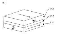
- the magnetoresistive element includes a magnetization free layer 113 whose magnetization direction changes according to an external magnetic field, a magnetization fixed layer 111 whose magnetization direction is fixed with respect to the external magnetic field, and a magnetization fixed layer. 111 and a nonmagnetic intermediate layer 112 sandwiched between the magnetization free layer 113 and the multilayer body.
- the magnetization of the magnetization free layer 113 is freely rotated within the film surface of the stacked body according to the external magnetic field.
- TMR tunnel magnetoresistive
- FIG. 8 shows how the conductance G changes with respect to the direction of the magnetic field applied from the outside to the TMR element.
- the horizontal axis indicates the rotation angle of the magnetic field
- the vertical axis indicates the conductance G.
- a TMR coupling body 116 and a TMR coupling body 117 in which eight TMR elements are coupled together constitute a half bridge (hereinafter referred to as a bridge), and this bridge is defined as an N pole
- a bridge this bridge is defined as an N pole
- the midpoint potential of the bridge is connected to the amplifier 119, which is disposed in front of the magnetic body 114 alternately magnetized to the S pole.
- the magnetization direction of the fixed layer of all TMR elements is in the direction of the arrow 118, and the direction 115 of the external magnetic field is as shown in FIG. Since the direction changes depending on the position as shown in the figure, the conductance G of the TMR connector 116 and the TMR connector 117 varies in a cosine wave shape.
- the conductance G of the TMR connector 116 and the TMR connector 117 is different in phase by 180 °.
- the midpoint potential of the bridge which is the connection point between the TMR connector 116 and the TMR connector 117, is calculated using the above Equation 2, and becomes the following Equation 3. (G0 + G1cos ⁇ ) / 2G0 (Equation 3)
- the voltage fluctuation of the midpoint potential has a cosine wave shape
- the output waveform of the output terminal 120 inverted and amplified by the amplifier 119 has a cosine wave shape like 121. In this way, it is possible to detect the movement of the magnetic body, which is the detected body, by converting the change in the magnetic field into a voltage.
- the nonmagnetic intermediate layer 112 is formed of an oxide film. Since the oxide film has only a thickness (several nm) at which the tunnel effect is generated, there is a concern that the oxide film may be destroyed due to an electrical factor or a physical factor due to foreign matter. Oxide film breakdown means that the TMR element becomes low resistance (or short).
- FIG. 10 shows a case where one connection 122 of 16 TMR elements connected fails. In this case, failure means low resistance (or short circuit). It is assumed that a magnetic field in the same direction is applied to 116 and 117 to which the TMR elements are connected. In this case, the output waveform 123 is offset to the high potential side as compared with the normal output waveform 124. For this reason, a failure can be detected from a deviation from a desired potential.
- a failure may not be detected depending on the number of TMR element failures connected.
- the configuration when it cannot be detected as a reference is shown in FIG. In FIG. 12, for example, if the resistance of the TMR element 1 connection is 2 K ⁇ and the normal voltage measurement value is 1.8 V, the six connections on the high potential side fail (short) across the midpoint potential, and the low potential The measured voltage when the side has two connected faults (short) is 1.8 V, and the fault may not be detected.
- the present invention has been made to solve the above-mentioned problems, and it is possible to reliably detect a low resistance (short circuit) or high resistance (unbreak) fault of a magnetoresistive element with a simpler configuration.
- An object of the present invention is to provide a magnetic detection device capable of performing the above.
- a bridge circuit is configured by connecting a first element and a second element, which are magnetoresistive elements whose resistance value changes with respect to an external magnetic field, in series.
- the other end of the bridge circuit is grounded, the connection point of the first element and the second element is connected to amplifying means, and one or more in series with the bridge circuit Switching means is connected, and one end of the output of the amplifying means is configured to be connected to the failure detection means.
- the magnetic detection device of the present invention it is possible to obtain a magnetic detection device that can reliably determine the failure of the magnetoresistive element with a simpler configuration without a small number of switches or switches.
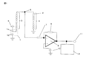
- FIG. 1 is a circuit configuration diagram showing a magnetic detection apparatus according to Embodiment 1 of the present invention.
- reference numeral 2 denotes one connection of TMR elements, and a bridge is constituted by TMR connectors 3 and 4 which are a set of eight connections.
- One end on the TMR connector 3 side is connected to the power source 5 via the switch 1.
- One end of the TMR connector 4 is grounded.
- a midpoint 6 of the bridge constituted by the TMR connector 3 and the TMR connector 4 is connected to a resistor 7.
- the resistors 7 and 8 are resistors that determine the magnification of an operational amplifier (hereinafter also referred to as an amplifier) 9.
- the positive side of the operational amplifier 9 is connected to the reference power supply 10.
- One end of the output of the operational amplifier 9 is connected to the failure detector 12.
- the present magnetic detection device When the switch 1 is connected to the power supply side contact 1a, the present magnetic detection device has the same circuit configuration as that of FIG. 9 described above, and the output terminal 11 with respect to the movement of the magnetic body 14 as described in the prior art. 9 has a cosine wave shape similar to the output waveform of FIG. 9, and the movement of the magnetic body 14 that is the detection target can be detected.
- the switch 1 is connected to the ground contact 1b.
- a magnetic field in the same direction is applied to the TMR connectors 3 and 4. This is because the TMR connectors 3 and 4 have the same resistance value.
- the positive electrode and the negative electrode of the operational amplifier 9 are imaginary shorted, the potential of the reference power source 10 of the positive electrode is applied to the series circuit of the resistor 7 and the combined resistance of the TMR connectors 3 and 4; Become.
- a current flowing in a series circuit constituted by the resistor 7 and the combined resistance of the TMR connectors 3 and 4 is converted into a voltage by the resistor 8 and output to the output terminal 11. This is a general current-voltage conversion circuit. If the resistance values of the resistors 7 and 8 are determined to be arbitrary values, the voltage of the output terminal 11 varies depending on the resistance value of the TMR connector 3 or the TMR connector 4. By measuring the voltage with the failure detector 12, the failure can be detected.
- the voltage value of the output terminal 11 is calculated using specific numerical values.
- One connection 2 of the TMR elements is 2 k ⁇ , the number of element connections of each of the TMR connections 3 and 4 is 8, the resistance value of the resistor 7 is 1 k ⁇ , the resistance value of the resistor 8 is 10 k ⁇ , and the voltage of the reference power supply 10 is 1V. Then, the voltage value of the output terminal 11 becomes 2.11V.
- the voltage value of the output terminal 11 is 2.25V. Since the voltage at the output terminal 11 changes in the case of such a failure, the failure of the TMR element can be detected by detecting the voltage change at the output terminal 11.
- the magnetic detection apparatus of the first embodiment of the present invention since one switch is provided and the current value flowing through the magnetoresistive element is converted into a voltage value using an amplifier, the TMR connection Even if the bodies 3 and 4 have the same number of connection failures, the failure can be detected.
- FIG. FIG. 2 is a circuit configuration diagram showing a magnetic detection apparatus according to Embodiment 2 of the present invention.
- reference numerals 13a and 13b denote switching devices. If the switch 1 of Embodiment 1 in FIG. 1 is omitted, the other configuration is the same as that in FIG.
- the magnetic detection device has the same circuit configuration as that of FIG. 9, and as described in the prior art, the waveform of the output terminal 11 is shown in FIG. It has a cosine wave shape similar to the output waveform, and can detect the movement of the magnetic body that is the detection target.
- the switch 13a is turned OFF. At this time, it is assumed that a magnetic field in the same direction is applied to the TMR connectors 3 and 4. Since the positive electrode and the negative electrode of the operational amplifier 9 are imaginary shorted, the potential of the reference power supply 10 of the positive electrode is applied to the series circuit of the resistor 7 and the TMR connector 4. The current flowing through the series circuit composed of the resistor 7 and the TMR connector 4 is converted into a voltage by the resistor 8 and output to the output terminal 11. Next, the switch 13a is turned on and 13b is turned off.
- the difference between the voltage of the power supply 5 and the voltage of the reference power supply 10 is applied to the series circuit of the TMR connector 3 and the resistor 7.
- the current flowing through the series circuit composed of the resistor 7 and the TMR connector 3 is converted into a voltage by the resistor 8 and output to the output terminal 11.
- the resistance values of the resistors 7 and 8 are determined to be arbitrary values, the voltage of the output terminal 11 changes depending on the resistance value of the TMR connector 3 or the TMR connector 4. Failure detection is possible.
- the voltage value of the output terminal 11 is calculated using specific numerical values.
- One connection 2 of the TMR element is 2 k ⁇ , the number of connections of the TMR connections 3 and 4 is eight, the resistance value of the resistor 7 is 1 k ⁇ , the resistance value of the resistor 8 is 10 k ⁇ , the voltage of the reference power supply 10 is 1 V, and the power supply 5 Is set to 2V.
- the switch 13a is turned off (the switch 13b is turned on)
- the voltage value of the output terminal 11 is 1.59V.
- the switch 13b is turned off (the switch 13a is turned on)
- the voltage value of the output terminal 11 is 0.41V.
- the voltage value of the output terminal 11 is 1.67V when the switch 13a is OFF and the output when the switch 13b is OFF.
- the voltage value of the terminal 11 is 0.33V.
- the magnetic detection device of the second embodiment of the present invention two switches are provided, and the current value flowing through the magnetoresistive element is converted into a voltage value using an amplifier. Even if the bodies 3 and 4 have the same number of connection failures, the failure can be detected.
- FIG. 3 is a circuit configuration diagram showing a magnetic detection device according to Embodiment 3 of the present invention.
- the magnetoresistive element has a so-called Wheatstone bridge configuration, which is substantially the same as that of the first embodiment except that a switch 14 is added.
- the waveform of the output terminal 11 with respect to the movement of the magnetic material is A cosine wave shape similar to that of the output waveform of FIG.
- the magnetoresistive element since the magnetoresistive element has a Wheatstone bridge configuration, the potential change at the connection point between 3a and 4a and the potential change at the connection point between the TMR connections 3b and 4b are different in phase by 180 °.
- Embodiment 1 FIG. As compared with the output 11, the output 11 can be doubled.
- the switch 1 is connected to the ground side contact 1b and the switch 14 is connected to 14b.
- a magnetic field in the same direction is applied to the TMR connectors 3a, 3b, 4a, and 4b. This is because the TMR connectors 3a, 3b, 4a, and 4b have the same resistance value. Since the positive electrode and the negative electrode of the operational amplifier 9 are imaginary shorted, the potential of the reference power supply 10 of the positive electrode is applied to the series circuit of the resistor 7a and the combined resistance of the TMR connectors 3a, 3b, 4a and 4b. It will be in the state.
- the current flowing through the series circuit formed by the resistor 7a and the combined resistance of the TMR connectors 3a, 3b, 4a, and 4b is converted into a voltage by the resistor 8a and output to the output terminal 11.
- the resistance values of the resistors 7a and 8a are set to arbitrary values, the voltage of the output terminal 11 varies depending on the resistance values of the TMR connectors 3a, 3b, 4a, and 4b. Therefore, failure detection becomes possible.
- the voltage value of the output terminal 11 is calculated using specific numerical values.
- the switch 1 is connected to the ground side contact 1b, and the switch 14 is connected to 14b.
- the resistor 7 a is 1 k ⁇
- the resistor 8 a is 10 k ⁇
- the reference power supply 10 is 1 V
- the output terminal 11 The voltage value of becomes 3V.
- the voltage value of the output terminal 11 is 3.11V.
- the magnetic detection device of the third embodiment of the present invention two switches are provided, and the current value flowing through the magnetoresistive element is converted into a voltage value using an amplifier. Even when the bodies 3a and 4a have the same number of connection failures, it is possible to detect the failure.
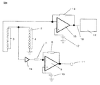
- FIG. 4 is a circuit configuration diagram showing a magnetic detection apparatus according to Embodiment 4 of the present invention.
- reference numeral 2 denotes one connection of TMR elements, and a bridge is constituted by TMR connectors 3 and 4 that are a set of eight connections.
- Reference numeral 19 denotes a buffer, and resistors 7 and 8 are resistors that determine the magnification of the operational amplifier 9.
- the power supply 10 is a reference potential of the output terminal 11 of the operational amplifier 9.
- the resistor 15, the operational amplifier 16 and the power supply 17 constitute a current-voltage conversion circuit.
- Reference numeral 12 denotes a failure detector.
- the waveform of the output terminal 11 becomes a cosine wave shape similar to the output waveform of FIG.
- the switching device is used.
- the configuration of the switching circuit may be difficult.
- the configuration of the fourth embodiment is effective when the configuration of such a switch is difficult.
- the TMR connectors 3 and 4 have the same number of connection failures. However, it is possible to detect a failure.
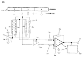
- FIG. 5 is a circuit configuration diagram showing a magnetic detection apparatus according to Embodiment 5 of the present invention.
- reference numeral 2 denotes one connection of TMR elements, and constitutes a TMR connection body 3 and a TMR connection body 4 which are a set of eight connections.
- the resistor 20, the operational amplifier 21, and the reference power supply 22 constitute a current-voltage conversion circuit.
- the resistor 23, the operational amplifier 24, and the reference power supply 25 constitute a current-voltage conversion circuit.
- the resistors 7a, 7b, 8a, 8b, the operational amplifier 9, and the reference power supply 10 constitute a differential amplifier.
- a failure detector 12 is connected to outputs 26 and 27 which are outputs of the operational amplifier 21 and the operational amplifier 24.
- FIG. 6 is a diagram for explaining the operation of the fifth embodiment.
- One end of the TMR connector 3 is connected to the negative side of the operational amplifier 21 that constitutes the current-voltage conversion circuit. Since the positive side and the negative side of the operational amplifier 21 are imaginary shorted, the potential of the reference power supply 22 is applied to the TMR connector 3.
- the TMR connector 4 has the same configuration, and the potential of the reference power supply 25 is applied to the TMR connector 4.
- Equation 3 the currents flowing in the TMR connector 3 and the TMR connector 4 are respectively expressed by the above-described Equation 1.
- Equation 3 the waveforms of the outputs 26 and 27 of the operational amplifiers 21 and 24 constituting the current-voltage conversion circuit have a cosine wave shape as shown by waveforms 33 and 34 in FIG.
- the outputs 26 and 27 of the operational amplifiers 21 and 24 are input to the operational amplifier 9 constituting differential amplification.
- the input waveform is amplified by the differential amplifier 9, and the waveform of the output terminal 11 becomes a cosine wave shape of 35 in FIG. 6, and thus the movement of the magnetic body as the detected body can be detected.
- a magnetic field 32 in the same direction is applied to the fixed layers of all the TMR elements of the TMR connector 3 and the TMR connector 4 in order to detect a failure of the TMR element.
- This is to make the TMR connectors 3 and 4 have a desired resistance value.
- the resistance values of the resistors 20 and 23 are assumed to be arbitrary values. Since the voltage of the output 26 or the output 27 changes depending on the resistance value of the TMR connector 3 or the TMR connector 4, the failure detector 12 can detect a failure by measuring the change in the voltage with the failure detector 12.
- the configuration of the switching circuit may be difficult, but the configuration of the fifth embodiment has a configuration of such a switch. Effective in difficult cases.
- the TMR connectors 3 and 4 have the same number of connection failures. However, it is possible to detect a failure.
- tunnel magnetoresistive element tunnel Magneto Resistance element
- the present invention is similarly implemented even when a giant magnetoresistive element (Giant Magneto Resistance element) is used. be able to.
- the embodiments can be appropriately modified and omitted within the scope of the invention.
- the present invention is a magnetic detection device that detects rotation of a detection target by a magnetic field change using a magnetoresistive element, and is suitable as a rotation sensor that detects rotation of a crankshaft or a camshaft of an automobile engine.
- 1 switch 2 connection of TMR elements, 3, 4 TMR connection body, 5 power supply, 6 bridge midpoint, 7, 8 resistors, 9 operational amplifier (amplifier), 10 reference power supply, 11 output terminal, 12 failure detectors, 13a, 13b, 14 switch, 15 resistors, 16 operational amplifiers, 17 power supplies, 18 output terminals, 19 buffers, 20 resistors, 21 operational amplifiers, 22 reference power supplies, 23 resistors, 24 operational amplifier, 25 reference power supply.
Landscapes
- Physics & Mathematics (AREA)
- Condensed Matter Physics & Semiconductors (AREA)
- General Physics & Mathematics (AREA)
- Measuring Magnetic Variables (AREA)
- Testing Of Short-Circuits, Discontinuities, Leakage, Or Incorrect Line Connections (AREA)
- Measurement Of Length, Angles, Or The Like Using Electric Or Magnetic Means (AREA)
- Transmission And Conversion Of Sensor Element Output (AREA)
- Hall/Mr Elements (AREA)
Abstract
Description
(非特許文献1の式(2)およびV.CONCLUSION欄参照。)
即ち、磁化固定層111の磁化方向に対して、磁化自由層113の磁化方向との相対角度をθとすると、コンダクタンスGは、次のように表される。ここで、磁化自由層113の磁化方向は、外部磁界の方向すなわち磁界の回転角θと一致する。
G=G0+G1cosθ ・・・・・・(数式1)
これを抵抗値で表現すると、数式1の逆数となる。
R=1/(G0+G1cosθ) ・・・・・(数式2)
図9において、磁性体114が紙面に向かって左方向に移動すれば、すべてのTMR素子の固定層の磁化方向は矢印118の方向にあり、図8に示したように外部磁界の方向115が図のように位置により方向が変わるため、TMR連結体116及びTMR連結体117のコンダクタンスGは余弦波形状に変動する。
(G0+G1cosθ)/2G0 ・・・・・(数式3)
中点電位の電圧変動は余弦波形状となり、増幅器119で反転増幅した出力端子120の出力波形は121のような余弦波形状になる。このようにして磁界の変化を電圧に変換して被検出体である磁性体の移動を検出できる。
(例えば、特許文献2参照。)
図10に16連結したTMR素子の1連結122が故障した場合を図示している。この場合故障とは低抵抗(乃至ショート)を意味する。TMR素子が連結された116と117は同一方向の磁界が印加されているとする。この場合、出力波形123は正常な出力波形124と比して、高電位側にオフセットしている。このため、所望の電位からのずれから故障を検出することができる。
図12において、例えば、TMR素子1連結の抵抗を2KΩとし、正常時の電圧測定値を1.8Vとすると、中点電位を挟んで高電位側の6連結が故障(ショート)し、低電位側が2連結故障(ショート)した場合の電圧測定値も1.8Vとなり、故障を検出できない場合がある。
なお、各図中、同一符号は、同一または相当部分を示すものとする。
図1は、この発明の実施の形態1に係る磁気検出装置を示す回路構成図である。
図1において、2はTMR素子の1連結で、8連結で一組としたTMR連結体3と4にてブリッジを構成している。TMR連結体3側の一端が電源5と切替器1を介して接続されている。またTMR連結体4の一端は接地されている。TMR連結体3とTMR連結体4で構成されるブリッジの中点6は抵抗器7に接続されている。抵抗器7と抵抗器8は、オペアンプ(以下増幅器ともいう。)9の倍率を決める抵抗器である。オペアンプ9のプラス側は基準電源10に接続されている。オペアンプ9の出力の一端は故障検出器12に接続されている。
TMR素子の1連結2を2kΩ、TMR連結体3と4各々の素子連結数を8個、抵抗器7の抵抗値を1kΩ、抵抗器8の抵抗値を10kΩ、基準電源10の電圧を1Vとすると、出力端子11の電圧値は2.11Vとなる。
ここで、TMR連結体3及び4の連結が故障によりそれぞれ1連結ずつ故障した場合、出力端子11の電圧値は2.25Vとなる。このように故障した場合に出力端子11の電圧が変化するため、出力端子11の電圧変化を検出することによってTMR素子の故障を検出することができる。
図2は、この発明の実施の形態2に係る磁気検出装置を示す回路構成図である。
図において13a、13bは切替器である。図1における実施の形態1の切替器1を省けば、その他の構成は図1と同一である。
抵抗器7と、TMR連結体4で構成される直列回路に流れる電流は抵抗器8により電圧に変換され、出力端子11に出力される。
次に、切替器13aをONにし、13bをOFFにする。オペアンプ9のプラス電極とマイナス電極はイマジナリーショートされているため、電源5の電圧と基準電源10の電圧との差がTMR連結体3と抵抗器7の直列回路に印加された状態となる。抵抗器7と、TMR連結体3で構成される直列回路に流れる電流は抵抗器8により電圧に変換され、出力端子11に出力される。ここで、抵抗器7及び抵抗器8の各々の抵抗値が任意の値に決められているものとすると、TMR連結体3もしくはTMR連結体4の抵抗値により、出力端子11の電圧が変わるため、故障検出が可能となる。
切替器13bをOFFにした場合(切替器13aはONにする)、出力端子11の電圧値は0.41Vとなる。ここでTMR連結体3及び4の連結が故障によりそれぞれ1連結ずつ故障した場合、切替器13aがOFFのとき、出力端子11の電圧値は1.67Vとなり、切替器13bがOFFのとき、出力端子11の電圧値は0.33Vとなる。
このように、故障した場合に出力端子11の電圧が変化するため、この電圧の変化を故障検出器12により測定することによって、故障を検出することができる。
図3は、この発明の実施の形態3に係る磁気検出装置を示す回路構成図である。
この発明の実施の形態3は、磁気抵抗素子がいわゆるホイートストンブリッジの構成となっており、実施の形態1に対して切替器14が追加されている以外はほぼ同じ構成となっている。図3において、切替器1が電源側接点1a側に、切替器14が14a側に接続されているときは、従来技術で説明したように、磁性体の動きに対して出力端子11の波形は図9の出力波形と同様の余弦波形状となり、被検出体である磁性体113の移動を検出できる。なお、実施の形態3では磁気抵抗素子がホイートストンブリッジの構成となっているため、3aと4aの接続点の電位変化とTMR連結3bと4bの接続点の電位変化は位相が180°異なるため、実施の形態1.と比して出力11は2倍の出力を得られる。
抵抗器7aと、TMR連結体3a、3b、4a、4bの合成抵抗で構成される直列回路に流れる電流は、抵抗器8aにより電圧に変換され、出力端子11に出力される。
ここで、抵抗器7a及び抵抗器8aの各々の抵抗値が任意の値に決められているものとすると、TMR連結体3a、3b、4a、4bの抵抗値により、出力端子11の電圧が変わるため、故障検出が可能となる。
このように、故障した場合に出力端子11の電圧が変化するため、この電圧の変化を故障検出器12により測定することによって、故障を検出することができる。
図4は、この発明の実施の形態4に係る磁気検出装置を示す回路構成図である。
図4において、2はTMR素子の1連結で、8連結で一組としたTMR連結体3と4にてブリッジを構成している。19はバッファであり、抵抗器7及び8はオペアンプ9の倍率を決める抵抗器である。電源10はオペアンプ9の出力端子11の基準電位である。また抵抗器15、オペアンプ16、電源17にて電流電圧変換回路を構成している。12は故障検出器である。
ここで、抵抗器15の抵抗値が任意の値に決められているものとすると、TMR連結体3もしくはTMR連結体4の抵抗値により、出力端子18の電圧が変わるため、この電圧の変化を故障検出器12により測定することによって、故障検出が可能となる。
図5は、この発明の実施の形態5に係る磁気検出装置を示す回路構成図である。
図5において、2はTMR素子の1連結で、8連結で一組としたTMR連結体3とTMR連結体4を構成している。抵抗器20、オペアンプ21、基準電源22は電流電圧変換回路を構成し、同様に抵抗器23、オペアンプ24、基準電源25は電流電圧変換回路を構成している。抵抗器7a、7b、8a、8b、オペアンプ9、基準電源10は差動増幅器を構成している。12は故障検出器であり、オペアンプ21とオペアンプ24の出力である出力26及び27とに接続される。
(G0+G1cosθ)VA ・・・・・・・・(数式3)
(G0+G1cos(θ+π))VA ・・・・・(数式4)
となる。ここで電流電圧変換回路を構成しているオペアンプ21、24の各々の出力26と27の波形は図6の波形33と34に示したように余弦波形状となる。
また、この発明は、その発明の範囲内において、実施の形態を適宜、変形、省略することが可能である。
5 電源、6 ブリッジの中点、7、8 抵抗器、
9 オペアンプ(増幅器)、10 基準電源、11 出力端子、
12 故障検出器、13a、13b、14 切替器、15 抵抗器、
16 オペアンプ、17電源、18 出力端子、19 バッファ、
20 抵抗器、21 オペアンプ、22 基準電源、23 抵抗器、
24 オペアンプ、25 基準電源。
Claims (7)
- 外部磁界に対して抵抗値が変化する磁気抵抗素子である第1の素子と第2の素子を直列に接続してブリッジ回路を構成し、
前記ブリッジ回路の一方の端は電源に接続され、
前記ブリッジ回路の他方の端は接地され、
前記第1の素子と前記第2の素子の接続点は増幅手段に接続され、
前記ブリッジ回路に直列に1つ以上の切替手段が接続され、
前記増幅手段の出力の一端は故障検出手段に接続されていることを特徴とする磁気検出装置。 - 外部磁界に対して抵抗値が変化する磁気抵抗素子である第1の素子と第2の素子が直列に接続され、前記磁気抵抗素子である第3の素子と第4の素子が直列に接続され、
前記第1と第2と第3と第4の素子はブリッジ回路を構成しており、
前記ブリッジ回路の一方の端は電源に接続され、
前記ブリッジ回路の他方の端は接地され、
前記第1の素子と前記第2の素子の接続点及び前記第3の素子と前記第4の素子の接続点は増幅手段に接続され、
前記ブリッジ回路に直列に1つ以上の切替手段が接続され、
前記ブリッジ回路と前記増幅手段との間に1つ以上の切替手段が接続され、
前記増幅手段の出力の一端は故障検出手段に接続されていることを特徴とする磁気検出装置。 - 外部磁界に対して抵抗値が変化する磁気抵抗素子である第1の素子と第2の素子が直列に接続されたブリッジ回路を構成しており、
前記ブリッジ回路の一方の端は電源に接続され、
前記ブリッジ回路の他方の端は接地され、
前記第1の素子と前記第2の素子の接続点は増幅手段に接続され、
前記電源と前記ブリッジ回路の中間には電流検出手段が接続され、
前記電流検出手段の出力の一端は故障検出手段に接続されていることを特徴とする磁気検出装置。 - 前記磁気抵抗素子は、外部磁界に対して磁化方向が固定された磁化固定層と、
外部磁界に応じて磁化方向が回転する磁化自由層と、前記磁化固定層と前記磁化自由層との間に挟まれた非磁性中間層からなることを特徴とする請求項1から請求項3の何れか1項に記載の磁気検出装置。 - 外部磁界に対して磁化方向が固定された磁化固定層と、
外部磁界に応じて磁化方向が回転する磁化自由層と、
前記磁化固定層と前記磁化自由層との間に挟まれた非磁性中間層からなる磁気抵抗素子であって、
前記磁気抵抗素子である第1の素子の一方の端は第1の電源に接続され、
前記第1の素子の他方の端は接地され、
前記磁気抵抗素子である第2の素子の一方の端は第2の電源に接続され、
前記第2の素子の他方の端は接地され、
前記各々の電源と前記第1の素子及び前記第2の素子の中間には各々電流検出手段が接続され、
前記各々の電流検出手段の出力が増幅手段に接続され、
前記電流検出手段の出力の一端は故障検出手段に接続されていることを
特徴とする磁気検出装置。 - 前記増幅手段は差動増幅手段であることを特徴とする請求項5に記載の磁気検出装置。
- 前記磁気抵抗素子は、トンネル効果磁気抵抗素子(TMR)であることを特徴とする磁気検出装置請求項1から請求項3および請求項5、請求項6のいずれか1項に記載の磁気検出装置。
Priority Applications (6)
| Application Number | Priority Date | Filing Date | Title |
|---|---|---|---|
| JP2015558644A JPWO2015111163A1 (ja) | 2014-01-23 | 2014-01-23 | 磁気検出装置 |
| CN201810794303.3A CN109001653B (zh) | 2014-01-23 | 2014-01-23 | 磁检测装置 |
| US14/915,476 US9983274B2 (en) | 2014-01-23 | 2014-01-23 | Magnetic detection device |
| CN201480072671.7A CN105899964B (zh) | 2014-01-23 | 2014-01-23 | 磁检测装置 |
| DE112014006248.0T DE112014006248T5 (de) | 2014-01-23 | 2014-01-23 | Magnetische Erfassungsvorrichtung |
| PCT/JP2014/051322 WO2015111163A1 (ja) | 2014-01-23 | 2014-01-23 | 磁気検出装置 |
Applications Claiming Priority (1)
| Application Number | Priority Date | Filing Date | Title |
|---|---|---|---|
| PCT/JP2014/051322 WO2015111163A1 (ja) | 2014-01-23 | 2014-01-23 | 磁気検出装置 |
Publications (1)
| Publication Number | Publication Date |
|---|---|
| WO2015111163A1 true WO2015111163A1 (ja) | 2015-07-30 |
Family
ID=53680994
Family Applications (1)
| Application Number | Title | Priority Date | Filing Date |
|---|---|---|---|
| PCT/JP2014/051322 WO2015111163A1 (ja) | 2014-01-23 | 2014-01-23 | 磁気検出装置 |
Country Status (5)
| Country | Link |
|---|---|
| US (1) | US9983274B2 (ja) |
| JP (1) | JPWO2015111163A1 (ja) |
| CN (2) | CN105899964B (ja) |
| DE (1) | DE112014006248T5 (ja) |
| WO (1) | WO2015111163A1 (ja) |
Families Citing this family (2)
| Publication number | Priority date | Publication date | Assignee | Title |
|---|---|---|---|---|
| EP3401646B1 (en) * | 2017-05-09 | 2020-04-15 | Melexis Technologies SA | Bridge sensor error check |
| CN113451995B (zh) * | 2021-08-31 | 2021-12-17 | 浙江大学杭州国际科创中心 | 一种短路和过流保护装置和方法 |
Citations (7)
| Publication number | Priority date | Publication date | Assignee | Title |
|---|---|---|---|---|
| JPH01128107U (ja) * | 1988-02-25 | 1989-09-01 | ||
| JPH10293040A (ja) * | 1997-04-17 | 1998-11-04 | Toyota Motor Corp | 検出装置 |
| JP3017061B2 (ja) * | 1994-11-04 | 2000-03-06 | インターナショナル・ビジネス・マシーンズ・コーポレイション | ブリッジ回路磁界センサー |
| JP2001194256A (ja) * | 1999-10-29 | 2001-07-19 | Denso Corp | センサ装置 |
| JP2004191189A (ja) * | 2002-12-11 | 2004-07-08 | Hitachi Unisia Automotive Ltd | ブリッジ型抵抗回路装置 |
| JP2008522146A (ja) * | 2004-11-25 | 2008-06-26 | コーニンクレッカ フィリップス エレクトロニクス エヌ ヴィ | 並列磁気センサーストリップを備えた磁気センサー |
| JP2013108887A (ja) * | 2011-11-22 | 2013-06-06 | Tokai Rika Co Ltd | 自己診断機能付センサ |
Family Cites Families (27)
| Publication number | Priority date | Publication date | Assignee | Title |
|---|---|---|---|---|
| JPS6070078U (ja) | 1983-10-21 | 1985-05-17 | 横河電機株式会社 | 警報回路 |
| GB2177561B (en) * | 1985-07-04 | 1989-05-10 | Terence Frank Hart | Electrical arc fault detector |
| US5351005A (en) * | 1992-12-31 | 1994-09-27 | Honeywell Inc. | Resetting closed-loop magnetoresistive magnetic sensor |
| JPH11194160A (ja) * | 1997-12-26 | 1999-07-21 | Teikoku Tsushin Kogyo Co Ltd | 磁気抵抗素子用増幅回路 |
| DE19834153A1 (de) * | 1998-07-29 | 2000-02-10 | Lust Antriebstechnik Gmbh | Verfahren zur Auswertung von Signalen magnetoresistiver Sensoren |
| US6343498B1 (en) | 1999-10-29 | 2002-02-05 | Denso Corporation | Physical quantity sensor having fault detection function |
| US6927566B2 (en) * | 2002-05-22 | 2005-08-09 | Ab Eletronik Gmbh | Device for generating output voltages |
| US6995957B2 (en) * | 2003-03-18 | 2006-02-07 | Hitachi Global Storage Technologies Netherland B.V. | Magnetoresistive sensor having a high resistance soft magnetic layer between sensor stack and shield |
| JP4405242B2 (ja) | 2003-11-20 | 2010-01-27 | NEC Avio赤外線テクノロジー株式会社 | センサの異常検出装置及びセンサの異常検出方法 |
| JP4302558B2 (ja) * | 2004-03-17 | 2009-07-29 | 三菱電機株式会社 | 回転状態検出装置及び回転状態検出方法 |
| FR2876800B1 (fr) * | 2004-10-18 | 2007-03-02 | Commissariat Energie Atomique | Procede et dispositif de mesure de champ magnetique a l'aide d'un capteur magnetoresitif |
| JP4486917B2 (ja) | 2005-10-24 | 2010-06-23 | アルプス電気株式会社 | 回転角検出センサ及びその故障検出回路 |
| US7262594B1 (en) * | 2006-03-24 | 2007-08-28 | Matsushita Electric Industrial Co., Ltd. | Rotation angle detector |
| JP4696994B2 (ja) * | 2006-03-24 | 2011-06-08 | パナソニック株式会社 | 回転角度検出装置 |
| EP2071350B1 (en) * | 2006-08-31 | 2015-03-25 | Alps Electric Co., Ltd. | Magnetism detecting apparatus |
| EP2153165B1 (en) * | 2007-05-29 | 2012-06-20 | Nxp B.V. | External magnetic field angle determination |
| JP5128399B2 (ja) * | 2008-07-18 | 2013-01-23 | 株式会社東海理化電機製作所 | 磁気センサデバイス |
| US8427144B2 (en) | 2009-07-28 | 2013-04-23 | Tdk Corporation | Magnetic sensor that includes magenetoresistive films and conductors that combine the magnetoresistive films |
| JP2011027683A (ja) * | 2009-07-29 | 2011-02-10 | Tdk Corp | 磁気センサ |
| JP5604652B2 (ja) * | 2010-02-23 | 2014-10-08 | アルプス・グリーンデバイス株式会社 | 電流センサ |
| JP5177197B2 (ja) * | 2010-10-13 | 2013-04-03 | Tdk株式会社 | 回転磁界センサ |
| US9013175B2 (en) * | 2010-11-26 | 2015-04-21 | Stmicroelectronics S.R.L. | Reading circuit for a magnetic field sensor with sensitivity calibration, and related reading method |
| JP5380425B2 (ja) * | 2010-12-28 | 2014-01-08 | 日立オートモティブシステムズ株式会社 | 磁界角計測装置,回転角計測装置およびそれを用いた回転機,システム,車両および車両駆動装置 |
| JP5832751B2 (ja) * | 2011-01-19 | 2015-12-16 | アルプス電気株式会社 | 自己診断可能な電子回路及び磁界検出装置 |
| JP6004758B2 (ja) * | 2012-06-07 | 2016-10-12 | エスアイアイ・セミコンダクタ株式会社 | 磁気センサ |
| JP2015049047A (ja) * | 2013-08-29 | 2015-03-16 | アルプス電気株式会社 | モータ制御装置 |
| US9506996B2 (en) * | 2013-10-17 | 2016-11-29 | Infineon Technologies Ag | Apparatus and method for detecting an error in a measurement of a quantity |
-
2014
- 2014-01-23 DE DE112014006248.0T patent/DE112014006248T5/de active Pending
- 2014-01-23 US US14/915,476 patent/US9983274B2/en active Active
- 2014-01-23 WO PCT/JP2014/051322 patent/WO2015111163A1/ja active Application Filing
- 2014-01-23 CN CN201480072671.7A patent/CN105899964B/zh active Active
- 2014-01-23 CN CN201810794303.3A patent/CN109001653B/zh active Active
- 2014-01-23 JP JP2015558644A patent/JPWO2015111163A1/ja active Pending
Patent Citations (7)
| Publication number | Priority date | Publication date | Assignee | Title |
|---|---|---|---|---|
| JPH01128107U (ja) * | 1988-02-25 | 1989-09-01 | ||
| JP3017061B2 (ja) * | 1994-11-04 | 2000-03-06 | インターナショナル・ビジネス・マシーンズ・コーポレイション | ブリッジ回路磁界センサー |
| JPH10293040A (ja) * | 1997-04-17 | 1998-11-04 | Toyota Motor Corp | 検出装置 |
| JP2001194256A (ja) * | 1999-10-29 | 2001-07-19 | Denso Corp | センサ装置 |
| JP2004191189A (ja) * | 2002-12-11 | 2004-07-08 | Hitachi Unisia Automotive Ltd | ブリッジ型抵抗回路装置 |
| JP2008522146A (ja) * | 2004-11-25 | 2008-06-26 | コーニンクレッカ フィリップス エレクトロニクス エヌ ヴィ | 並列磁気センサーストリップを備えた磁気センサー |
| JP2013108887A (ja) * | 2011-11-22 | 2013-06-06 | Tokai Rika Co Ltd | 自己診断機能付センサ |
Also Published As
| Publication number | Publication date |
|---|---|
| CN105899964B (zh) | 2019-09-24 |
| US9983274B2 (en) | 2018-05-29 |
| CN109001653A (zh) | 2018-12-14 |
| CN109001653B (zh) | 2021-09-14 |
| JPWO2015111163A1 (ja) | 2017-03-23 |
| CN105899964A (zh) | 2016-08-24 |
| US20160223625A1 (en) | 2016-08-04 |
| DE112014006248T5 (de) | 2016-10-13 |
Similar Documents
| Publication | Publication Date | Title |
|---|---|---|
| US8466676B2 (en) | Magnetic sensor with bridge circuit including magnetoresistance effect elements | |
| JP4807535B2 (ja) | 磁気センサ | |
| CN103376426B (zh) | 磁场传感器 | |
| US9910106B2 (en) | Magnetic field sensor with increased linearity | |
| JP6255902B2 (ja) | 磁界検出装置 | |
| US20100123458A1 (en) | Twin vertical hall sensor | |
| WO2015137277A1 (ja) | 磁気センサー | |
| WO2015111163A1 (ja) | 磁気検出装置 | |
| JP2015078949A (ja) | ホール起電力信号検出回路 | |
| US11243275B2 (en) | Magnetic field sensing device | |
| JP6309067B2 (ja) | 磁気検出装置 | |
| US20140125328A1 (en) | Magnetic detection device | |
| JP2016142652A (ja) | 電力センサー | |
| TWI703338B (zh) | 電流感測器 | |
| TWI714107B (zh) | 電流感測器 | |
| JP2011007569A (ja) | 磁気検出装置及び磁気検出装置のテスト方法 | |
| US10788342B2 (en) | Magnetic field sensor and magnetic field sensing method | |
| JPS6191577A (ja) | 回転磁界検出装置 | |
| JP2020041869A (ja) | 磁気センサ | |
| JP2014235080A (ja) | 磁気抵抗素子および磁気センサ | |
| JP2008527370A (ja) | 角度センサ | |
| JP2014066565A (ja) | 磁気センサ | |
| CN110857951A (zh) | 电流传感器 | |
| JP2016121944A (ja) | 磁気抵抗素子回路及びブリッジ回路 | |
| JP2011017614A (ja) | 磁気式位置検出装置 |
Legal Events
| Date | Code | Title | Description |
|---|---|---|---|
| 121 | Ep: the epo has been informed by wipo that ep was designated in this application |
Ref document number: 14879470 Country of ref document: EP Kind code of ref document: A1 |
|
| ENP | Entry into the national phase |
Ref document number: 2015558644 Country of ref document: JP Kind code of ref document: A |
|
| WWE | Wipo information: entry into national phase |
Ref document number: 14915476 Country of ref document: US |
|
| WWE | Wipo information: entry into national phase |
Ref document number: 112014006248 Country of ref document: DE |
|
| 122 | Ep: pct application non-entry in european phase |
Ref document number: 14879470 Country of ref document: EP Kind code of ref document: A1 |