WO2015102029A1 - コンピュータ装置用の識別子提供装置 - Google Patents
コンピュータ装置用の識別子提供装置 Download PDFInfo
- Publication number
- WO2015102029A1 WO2015102029A1 PCT/JP2013/085287 JP2013085287W WO2015102029A1 WO 2015102029 A1 WO2015102029 A1 WO 2015102029A1 JP 2013085287 W JP2013085287 W JP 2013085287W WO 2015102029 A1 WO2015102029 A1 WO 2015102029A1
- Authority
- WO
- WIPO (PCT)
- Prior art keywords
- conductive layer
- silver
- layer pattern
- thickness
- predetermined
- Prior art date
Links
Images


Classifications
-
- G—PHYSICS
- G06—COMPUTING; CALCULATING OR COUNTING
- G06F—ELECTRIC DIGITAL DATA PROCESSING
- G06F3/00—Input arrangements for transferring data to be processed into a form capable of being handled by the computer; Output arrangements for transferring data from processing unit to output unit, e.g. interface arrangements
- G06F3/01—Input arrangements or combined input and output arrangements for interaction between user and computer
- G06F3/03—Arrangements for converting the position or the displacement of a member into a coded form
- G06F3/041—Digitisers, e.g. for touch screens or touch pads, characterised by the transducing means
- G06F3/044—Digitisers, e.g. for touch screens or touch pads, characterised by the transducing means by capacitive means
- G06F3/0443—Digitisers, e.g. for touch screens or touch pads, characterised by the transducing means by capacitive means using a single layer of sensing electrodes
-
- G—PHYSICS
- G06—COMPUTING; CALCULATING OR COUNTING
- G06F—ELECTRIC DIGITAL DATA PROCESSING
- G06F3/00—Input arrangements for transferring data to be processed into a form capable of being handled by the computer; Output arrangements for transferring data from processing unit to output unit, e.g. interface arrangements
- G06F3/01—Input arrangements or combined input and output arrangements for interaction between user and computer
- G06F3/03—Arrangements for converting the position or the displacement of a member into a coded form
- G06F3/041—Digitisers, e.g. for touch screens or touch pads, characterised by the transducing means
- G06F3/044—Digitisers, e.g. for touch screens or touch pads, characterised by the transducing means by capacitive means
-
- G—PHYSICS
- G06—COMPUTING; CALCULATING OR COUNTING
- G06F—ELECTRIC DIGITAL DATA PROCESSING
- G06F3/00—Input arrangements for transferring data to be processed into a form capable of being handled by the computer; Output arrangements for transferring data from processing unit to output unit, e.g. interface arrangements
- G06F3/01—Input arrangements or combined input and output arrangements for interaction between user and computer
- G06F3/03—Arrangements for converting the position or the displacement of a member into a coded form
- G06F3/033—Pointing devices displaced or positioned by the user, e.g. mice, trackballs, pens or joysticks; Accessories therefor
- G06F3/039—Accessories therefor, e.g. mouse pads
- G06F3/0393—Accessories for touch pads or touch screens, e.g. mechanical guides added to touch screens for drawing straight lines, hard keys overlaying touch screens or touch pads
-
- G—PHYSICS
- G06—COMPUTING; CALCULATING OR COUNTING
- G06F—ELECTRIC DIGITAL DATA PROCESSING
- G06F3/00—Input arrangements for transferring data to be processed into a form capable of being handled by the computer; Output arrangements for transferring data from processing unit to output unit, e.g. interface arrangements
- G06F3/01—Input arrangements or combined input and output arrangements for interaction between user and computer
- G06F3/03—Arrangements for converting the position or the displacement of a member into a coded form
- G06F3/041—Digitisers, e.g. for touch screens or touch pads, characterised by the transducing means
- G06F3/044—Digitisers, e.g. for touch screens or touch pads, characterised by the transducing means by capacitive means
- G06F3/0448—Details of the electrode shape, e.g. for enhancing the detection of touches, for generating specific electric field shapes, for enhancing display quality
-
- H—ELECTRICITY
- H05—ELECTRIC TECHNIQUES NOT OTHERWISE PROVIDED FOR
- H05K—PRINTED CIRCUITS; CASINGS OR CONSTRUCTIONAL DETAILS OF ELECTRIC APPARATUS; MANUFACTURE OF ASSEMBLAGES OF ELECTRICAL COMPONENTS
- H05K1/00—Printed circuits
- H05K1/02—Details
- H05K1/0266—Marks, test patterns or identification means
-
- H—ELECTRICITY
- H05—ELECTRIC TECHNIQUES NOT OTHERWISE PROVIDED FOR
- H05K—PRINTED CIRCUITS; CASINGS OR CONSTRUCTIONAL DETAILS OF ELECTRIC APPARATUS; MANUFACTURE OF ASSEMBLAGES OF ELECTRICAL COMPONENTS
- H05K1/00—Printed circuits
- H05K1/02—Details
- H05K1/0275—Security details, e.g. tampering prevention or detection
-
- H—ELECTRICITY
- H05—ELECTRIC TECHNIQUES NOT OTHERWISE PROVIDED FOR
- H05K—PRINTED CIRCUITS; CASINGS OR CONSTRUCTIONAL DETAILS OF ELECTRIC APPARATUS; MANUFACTURE OF ASSEMBLAGES OF ELECTRICAL COMPONENTS
- H05K1/00—Printed circuits
- H05K1/02—Details
- H05K1/0286—Programmable, customizable or modifiable circuits
- H05K1/0292—Programmable, customizable or modifiable circuits having a modifiable lay-out, i.e. adapted for engineering changes or repair
-
- H—ELECTRICITY
- H05—ELECTRIC TECHNIQUES NOT OTHERWISE PROVIDED FOR
- H05K—PRINTED CIRCUITS; CASINGS OR CONSTRUCTIONAL DETAILS OF ELECTRIC APPARATUS; MANUFACTURE OF ASSEMBLAGES OF ELECTRICAL COMPONENTS
- H05K1/00—Printed circuits
- H05K1/02—Details
- H05K1/09—Use of materials for the conductive, e.g. metallic pattern
- H05K1/092—Dispersed materials, e.g. conductive pastes or inks
- H05K1/095—Dispersed materials, e.g. conductive pastes or inks for polymer thick films, i.e. having a permanent organic polymeric binder
-
- H—ELECTRICITY
- H05—ELECTRIC TECHNIQUES NOT OTHERWISE PROVIDED FOR
- H05K—PRINTED CIRCUITS; CASINGS OR CONSTRUCTIONAL DETAILS OF ELECTRIC APPARATUS; MANUFACTURE OF ASSEMBLAGES OF ELECTRICAL COMPONENTS
- H05K1/00—Printed circuits
- H05K1/02—Details
- H05K1/09—Use of materials for the conductive, e.g. metallic pattern
- H05K1/092—Dispersed materials, e.g. conductive pastes or inks
- H05K1/097—Inks comprising nanoparticles and specially adapted for being sintered at low temperature
-
- H—ELECTRICITY
- H05—ELECTRIC TECHNIQUES NOT OTHERWISE PROVIDED FOR
- H05K—PRINTED CIRCUITS; CASINGS OR CONSTRUCTIONAL DETAILS OF ELECTRIC APPARATUS; MANUFACTURE OF ASSEMBLAGES OF ELECTRICAL COMPONENTS
- H05K3/00—Apparatus or processes for manufacturing printed circuits
- H05K3/10—Apparatus or processes for manufacturing printed circuits in which conductive material is applied to the insulating support in such a manner as to form the desired conductive pattern
- H05K3/12—Apparatus or processes for manufacturing printed circuits in which conductive material is applied to the insulating support in such a manner as to form the desired conductive pattern using thick film techniques, e.g. printing techniques to apply the conductive material or similar techniques for applying conductive paste or ink patterns
- H05K3/1216—Apparatus or processes for manufacturing printed circuits in which conductive material is applied to the insulating support in such a manner as to form the desired conductive pattern using thick film techniques, e.g. printing techniques to apply the conductive material or similar techniques for applying conductive paste or ink patterns by screen printing or stencil printing
- H05K3/1233—Methods or means for supplying the conductive material and for forcing it through the screen or stencil
-
- G—PHYSICS
- G06—COMPUTING; CALCULATING OR COUNTING
- G06F—ELECTRIC DIGITAL DATA PROCESSING
- G06F2203/00—Indexing scheme relating to G06F3/00 - G06F3/048
- G06F2203/041—Indexing scheme relating to G06F3/041 - G06F3/045
- G06F2203/04103—Manufacturing, i.e. details related to manufacturing processes specially suited for touch sensitive devices
-
- G—PHYSICS
- G06—COMPUTING; CALCULATING OR COUNTING
- G06F—ELECTRIC DIGITAL DATA PROCESSING
- G06F2203/00—Indexing scheme relating to G06F3/00 - G06F3/048
- G06F2203/041—Indexing scheme relating to G06F3/041 - G06F3/045
- G06F2203/04104—Multi-touch detection in digitiser, i.e. details about the simultaneous detection of a plurality of touching locations, e.g. multiple fingers or pen and finger
-
- H—ELECTRICITY
- H05—ELECTRIC TECHNIQUES NOT OTHERWISE PROVIDED FOR
- H05K—PRINTED CIRCUITS; CASINGS OR CONSTRUCTIONAL DETAILS OF ELECTRIC APPARATUS; MANUFACTURE OF ASSEMBLAGES OF ELECTRICAL COMPONENTS
- H05K1/00—Printed circuits
- H05K1/02—Details
- H05K1/03—Use of materials for the substrate
- H05K1/0386—Paper sheets
-
- H—ELECTRICITY
- H05—ELECTRIC TECHNIQUES NOT OTHERWISE PROVIDED FOR
- H05K—PRINTED CIRCUITS; CASINGS OR CONSTRUCTIONAL DETAILS OF ELECTRIC APPARATUS; MANUFACTURE OF ASSEMBLAGES OF ELECTRICAL COMPONENTS
- H05K2201/00—Indexing scheme relating to printed circuits covered by H05K1/00
- H05K2201/02—Fillers; Particles; Fibers; Reinforcement materials
- H05K2201/0203—Fillers and particles
- H05K2201/0242—Shape of an individual particle
- H05K2201/0245—Flakes, flat particles or lamellar particles
-
- H—ELECTRICITY
- H05—ELECTRIC TECHNIQUES NOT OTHERWISE PROVIDED FOR
- H05K—PRINTED CIRCUITS; CASINGS OR CONSTRUCTIONAL DETAILS OF ELECTRIC APPARATUS; MANUFACTURE OF ASSEMBLAGES OF ELECTRICAL COMPONENTS
- H05K2201/00—Indexing scheme relating to printed circuits covered by H05K1/00
- H05K2201/03—Conductive materials
- H05K2201/032—Materials
- H05K2201/0326—Inorganic, non-metallic conductor, e.g. indium-tin oxide [ITO]
-
- H—ELECTRICITY
- H05—ELECTRIC TECHNIQUES NOT OTHERWISE PROVIDED FOR
- H05K—PRINTED CIRCUITS; CASINGS OR CONSTRUCTIONAL DETAILS OF ELECTRIC APPARATUS; MANUFACTURE OF ASSEMBLAGES OF ELECTRICAL COMPONENTS
- H05K2203/00—Indexing scheme relating to apparatus or processes for manufacturing printed circuits covered by H05K3/00
- H05K2203/01—Tools for processing; Objects used during processing
- H05K2203/0104—Tools for processing; Objects used during processing for patterning or coating
- H05K2203/0139—Blade or squeegee, e.g. for screen printing or filling of holes
-
- H—ELECTRICITY
- H05—ELECTRIC TECHNIQUES NOT OTHERWISE PROVIDED FOR
- H05K—PRINTED CIRCUITS; CASINGS OR CONSTRUCTIONAL DETAILS OF ELECTRIC APPARATUS; MANUFACTURE OF ASSEMBLAGES OF ELECTRICAL COMPONENTS
- H05K2203/00—Indexing scheme relating to apparatus or processes for manufacturing printed circuits covered by H05K3/00
- H05K2203/11—Treatments characterised by their effect, e.g. heating, cooling, roughening
- H05K2203/1131—Sintering, i.e. fusing of metal particles to achieve or improve electrical conductivity
Definitions
- the present invention relates to an identifier providing apparatus that provides a unique identifier as a command for causing an information processing apparatus including a computer apparatus to execute predetermined information processing.
- a capacitive touch panel or a capacitive touch pad (hereinafter also referred to as “capacitive touch device”).
- capacitive touch device There are computer devices such as tablets and smartphones (hereinafter referred to as “touch computer devices”).
- the touch computer device is configured to start execution of predetermined information processing when the user touches the touch panel with a predetermined number of fingers (multi-touch), for example.
- the touch computer apparatus acquires the number of touch points of the user's multi-touch and the coordinates of each touch point, and performs information processing set in advance according to the number of touch points of the multi-touch and the coordinates of each touch point. Perform the action.
- a separate independent (separate) driving device that is paired with an information processing device having a capacitive multi-touch display is brought into contact with the multi-touch display of the information processing device, thereby
- the present invention relates to an information processing system using a multi-touch function for causing a device to execute desired information processing, and more particularly, to a driving device for the information processing device, and an information processing system including the information processing device and the driving device.
- the present invention makes it possible to easily and reliably perform multi-touch on a multi-touch display, and even in the case of a small multi-touch display, a plurality of fingers can be touched accurately and simultaneously at a predetermined plurality of contact positions. The challenge is to do so.
- the present invention presses the information processing device against the opposing surface of the driving device, so that the contact portion of the predetermined arrangement mode has a contact area (screen) of the corresponding arrangement mode in the multi-touch display.
- the button storage area is set to contact the information processing device and the corresponding processing (content display processing, etc.) is executed, and the charge storage unit contacts the contact unit through the conduction unit. It is configured to allow charge transfer in the region and to reliably cause a capacitance change in the contact region.
- the invention of the drive device can also be applied to an identifier providing device that provides a unique identifier as a command for causing an information processing device including a computer device to execute predetermined information processing.
- a drive device that specifically implements the present invention provides a predetermined conductive layer pattern (described above) on the surface of a base or base made of an insulator. It is necessary to form a pattern of conductive layers formed by disposing the contact portions in a predetermined arrangement manner, and a predetermined capacitance is provided in the feeding area of the multi-touch display via the conductive layer pattern.
- the present inventors have confirmed in the course of earnest research and development that it is necessary to apply a considerable amount of silver paste to the base.
- the inventors of the present invention may have a relatively large thickness of the conductive layer pattern itself due to the large amount of silver paste on the base, and a considerable area of the conductive layer pattern may be required. This was confirmed by experiments and the like.
- the silver paste as the raw material of the conductive layer pattern is very expensive. In the above drive device invention, it is expected that the manufacturing cost will greatly increase even if mass production is attempted.
- a predetermined pattern of silver paste is applied on the base to form a conductive layer pattern, it is preferable to use screen printing or the like from the viewpoint of mass productivity.
- a large amount of silver is used on the base.
- the present inventors have confirmed that the quality after production may be uneven and the yield may be considerably reduced.
- the present invention provides a minimum required amount of silver paste on the surface of a base made of an insulator in order to provide a unique identifier as a command for causing an information processing device made of a computer device to execute predetermined information processing.
- a conductive layer pattern with an extremely small thickness and the minimum necessary area, the electrical conductivity (resistivity) necessary for causing the computer device to execute the predetermined information processing operation is achieved.
- the manufacturing cost can be greatly reduced, and even if a conductive layer pattern with a minimum thickness / minimum area is formed with the minimum required amount of silver paste, a sufficiently good yield can be achieved and mass production can be achieved. It is an object of the present invention to provide an identifier providing device that can be realized.
- An identifier providing device for a computer device is an identifier providing device that provides a unique identifier as a command for causing an information processing device including a computer device to execute predetermined information processing.
- the identifier providing device includes a base material as an insulator (typically a solid in a predetermined form made of an insulating material), and a predetermined surface (typically a predetermined range and / or a predetermined area) of the base material. And a conductive layer pattern formed by applying a silver paste to form a predetermined pattern by printing.
- the silver paste for forming the conductive layer pattern has a particle diameter d in the range of 3.0 to 5.0 ⁇ m (preferably 3.5 to 4.5 ⁇ m) as silver particles, and the thickness of the maximum thickness portion. Only silver flakes having T11 of 100 nm or less (preferably 50 nm or less) and the minimum thickness T13 of 50 nm or less (for example, 30 to 50 nm, preferably 20 to 30 nm) are contained.
- the conductive layer pattern is formed such that the film thickness T2 is within a range of 10 ⁇ m or less (preferably 5 to 6 ⁇ m) by laminating the silver flakes in the thickness direction (typically substantially parallel). Yes.
- the silver flakes forming the conductive layer are in a fused state or a cohesive contact state with each other at the minimum thickness portion.
- the present invention provides only a minimum amount of silver paste on the surface of a base including an insulator.
- the electrical conductivity (resistivity) necessary for causing the computer device to execute the predetermined information processing operation is achieved.
- the production cost can be greatly reduced, and even if the conductive layer pattern with the minimum thickness / minimum area is formed with the minimum required amount of silver paste, a sufficiently good yield can be achieved and mass production can be achieved. Can be planned.
- FIG. 1 is a plan view showing an identifier providing apparatus for a computer apparatus according to Embodiment 1 of the present invention.
- FIG. 2 is a bottom view showing the surface on the conductive layer pattern side of the identifier providing device for a computer device according to Embodiment 1 of the present invention.
- FIG. 3 is a bottom view showing a surface on the conductive layer pattern side of the identifier providing device for a computer device according to Embodiment 1 of the present invention, where (a) shows a state where a primary coat is formed, and (b) The state which formed the secondary coat is shown.
- FIG. 1 is a plan view showing an identifier providing apparatus for a computer apparatus according to Embodiment 1 of the present invention.
- FIG. 2 is a bottom view showing the surface on the conductive layer pattern side of the identifier providing device for a computer device according to Embodiment 1 of the present invention.
- FIG. 3 is a bottom view showing a surface on the conductive layer pattern side of the identifie
- FIG. 4 is a process diagram showing a process of forming an identifier providing apparatus for a computer device according to Embodiment 1 of the present invention, (a) showing a conductive pattern forming process, and (b) a primary coat forming process.
- FIG. 5 is a process diagram showing a process of forming an identifier providing apparatus for a computer apparatus according to Embodiment 1 of the present invention, (a) showing a secondary coat forming process, and (b) showing a pattern forming process.
- FIG. 6 is a cross-sectional view showing a cross section of the conductive layer pattern (and a cross section of the surface coating) of the identifier providing device for a computer device according to Embodiment 1 of the present invention.
- FIG. 7 is a sectional view showing an identifier providing apparatus for a computer apparatus according to Embodiment 1 of the present invention.
- FIG. 8 is a sectional view showing an identifier providing apparatus for a computer apparatus according to Embodiment 1 of the present invention.
- FIG. 9 is a sectional view showing an identifier providing device for a computer device according to Embodiment 1 of the present invention.
- FIG. 10 is a cross-sectional view showing an identifier providing device for a computer device according to Embodiment 1 of the present invention.
- FIG. 11 is a sectional view showing an identifier providing device for a computer device according to Embodiment 1 of the present invention.
- FIG. 12 is an explanatory diagram showing silver flakes for forming a conductive layer pattern of the identifier providing device for a computer device according to Embodiment 1 of the present invention.
- FIG. 13 is an explanatory diagram showing a partially fused structure of selected silver flakes in a stacked state in a conductive layer pattern of the identifier providing device for a computer device according to Embodiment 1 of the present invention.
- FIG. 14 is an explanatory diagram showing a conductive pattern forming step (screen printing) of the identifier providing device for a computer device according to the first embodiment of the present invention.
- FIG. 15 is an explanatory diagram showing manufacturing parameters (raw material viscosity, squeegee speed, printing pressure, attack angle) in the conductive pattern forming step (screen printing) of the identifier providing device for a computer device according to Embodiment 1 of the present invention. is there.
- FIG. 16 is an explanatory diagram showing screen printing in the conductive pattern forming step of the identifier providing device for a computer device according to the first embodiment of the present invention.
- FIG. 17 is an explanatory diagram showing a conductive pattern forming step (screen printing) of the identifier providing device for a computer device according to the first embodiment of the present invention.
- FIG. 18 is an explanatory diagram showing a conductive pattern forming step (screen printing) of the identifier providing device for a computer device according to the first embodiment of the present invention.
- FIG. 19 is a plan view showing an identifier providing apparatus for a computer apparatus according to Embodiment 2 of the present invention.
- FIG. 20 is a plan view showing an identifier providing apparatus for a computer apparatus according to Embodiment 3 of the present invention.
- the present invention can be embodied as the identifier providing apparatus of the embodiment (Embodiment 1) shown in FIGS.
- this identifier providing apparatus will be described with reference to FIGS.
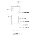
- the identifier providing apparatus according to the present embodiment is integrally formed with a base material 10 integrally formed to have a predetermined shape and a predetermined range of the surface of the base material 10 as shown in FIG.
- the conductive layer pattern 20 is provided.
- the configuration of each unit of the identifier providing device will be described in detail.
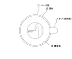
- the base material 10 is formed by integrally forming a tab 12 as a grip portion having a predetermined shape on a base portion 11 having a predetermined shape. More specifically, the base portion 11 has a perfect circular sheet shape.
- the tab 12 has a semi-track shape sheet shape obtained by cutting an oval or track-shaped sheet material in half in the length direction.
- the tab 12 is joined so that the base end thereof is integrally continuous with a predetermined angular position of the outer peripheral edge of the base portion 11, and is in the same plane as the base portion 11. Extends outward in the radial direction of the base 11.
- the base material 10 is integrally formed so as to have a sheet shape (shown in FIG. 1) composed of the base portion 11 and the tab 12 by a single sheet of paper having a predetermined paper quality.
- the base material 10 can be formed from an arbitrary insulator (a solid having a predetermined shape made of a non-conductive material or an insulating material), for example, an electrically insulating material (dielectric material) such as a paper material, a wood material, or a synthetic resin. In some cases, as long as it is an insulator, it can also be formed of an inorganic material such as a stone material. However, the base material 10 is typically formed in a thin sheet shape (a sheet shape having a wall thickness equivalent to that of a normal paper sheet) such as a paper sheet made of a paper material or a synthetic resin sheet made of a synthetic resin material. . As shown in FIG. 1, a predetermined pattern 13 is provided on the surface of the base portion 11 of the base material 10 by printing or the like. However, the pattern 13 may not be provided.
- the conductive layer pattern 20 includes a finger contact portion 21 as a human body side grounding portion, an extension portion 22 as a general-purpose conductor portion, a conduction portion 23 as an individual conductor portion, and a PC drive.
- This is a conductive layer having a predetermined pattern shape including the PC side contact portion 24 as a portion.
- the conductive layer pattern 20 is a predetermined scale-like, flake-like or flake-like silver particle (hereinafter referred to as “silver flake”), and is prepared and / or selected so as to have a uniform particle size with a minimum thickness.
- a slurry-like silver paste ink containing the obtained silver flakes (hereinafter sometimes referred to as “selected silver flakes”) is applied to the surface of the base portion 11 of the substrate 10 (typically screen printing or the like). Are applied to form a predetermined pattern). More specifically, the finger contact portion 21 is applied to the entire back surface of the tab 12 of the base material 10 by printing and integrally laminated to form a coating film shape corresponding to the tab 12.
- the extending portion 22 is integrally formed and laminated on the back surface of the base portion 11 of the base material 10 by printing so as to extend within a predetermined angle range on both sides in the circumferential direction (directions away from each other) with the tab 12 as the center.
- An arch-like coating film having a predetermined extending angle ⁇ is formed.
- the conductive portion 23 is formed in the direction parallel to the diameter direction of the base portion 11 (hereinafter, also referred to as “diameter parallel direction”) from the inner peripheral edge of the extending portion 22 on the back surface of the base portion 11 of the base material 10. It is applied by printing so as to extend linearly (and extend in a direction parallel to the major axis direction of the tab 11), and is integrally laminated to form a predetermined width d (hereinafter referred to as “conductor width d”). There is a linear thin line-like coating film.
- the PC-side contact portion 24 is integrally laminated by applying it to the front end of the conduction portion 23 on the back surface of the base portion 11 of the base material 10 by printing, and has a predetermined diameter W (hereinafter referred to as “contact portion diameter W”). It has a perfect circular film shape.
- the base material 10 includes the base portion 11 as a main portion and the grip portion 12 as an attachment portion formed continuously at one end of the base portion 11.
- the base portion 11 has a first dimension in the first direction (vertical direction in FIG. 2) (vertical dimension from the upper end to the lower end in FIG. 2, ie, a diameter in the vertical direction), and the first dimension.
- a second dimension (left and right dimension in FIG. 2 (excluding the grip portion 12) from the left end to the right end, that is, the diameter in the left and right direction) in a second direction (right and left direction in FIG. 2) orthogonal to the direction of have.
- the finger contact portion 21 of the conductive layer pattern 20 is formed on the back surface of the grip portion 12 and is electrically connected to the user's finger when the user's finger grips the grip portion 12 of the base material 10. It has a planar shape with a predetermined area as the conductive layer portion.
- the extending portion 22 extends on the back surface of the base portion 11 so as to intersect the first direction, and is a predetermined second conductive layer portion formed by being electrically connected to the finger contact portion 21. It has a surface shape.
- a plurality of predetermined conductive portions 23 are provided, each extending linearly from the extending portion 22 to the first direction of the base portion 11 on the back surface of the base portion 11.
- a conductive wire is formed as a third conductive layer portion formed by being electrically connected to the extended portion 22.
- the PC-side contact portion 24 is provided in the same plural number (three in the illustrated example) as the conductive portion 23, and each is formed by electrically connecting to the tip of the conductive portion 23 on the back surface of the base portion 11.
- the fourth conductive layer portion has a planar shape with a predetermined area. And the surface (back surface) by the side of the conductive layer pattern 20 of the base part 11 of the base material 10 was made to contact
- the PC-side contact portion 24 of the conductive layer pattern 20 is electrically connected to the user's finger through the conductive portion 23, the extending portion 22 and the finger contact portion 21 to cause a capacitance change in the touch panel.
- the extending portion 22 of the conductive layer pattern 20 is formed by replacing the two PC side contact portions 24 (the upper and lower PC side contact portions 24 in the example of FIG. 2) of the plurality of PC side contact portions 24 with the base portion 11. 2 of the conductive parts 23 formed at the leading ends of the two conductive parts 23 (in FIG. 2). Are extended at a predetermined extension angle so as to extend to the base end position of the upper and lower conductive portions 23).
- Extension angle ⁇ of extension part 22 (one of the features of the present invention)
- the extending portion 22 has an extending angle ⁇ within the range of the semicircular portion of one of the base portions 11 (that is, the tab 12 side) having a perfect circular shape.
- the base portion 11 is provided with a predetermined angle within the angular range of the outer peripheral edge of the semicircular portion (that is, within the angular range of 180 degrees on the tab 12 side).
- the extending angle ⁇ of the extending portion 22 is obtained by extending the linear conducting portion 23 from both ends in the circumferential direction of the extending portion 22 in a diameter parallel direction (parallel to the diameter direction of the base portion 11).
- the arrangement position of the PC-side contact portion 24 having a predetermined diameter W connected to the tip is set so as to cover the entire range of the back surface of the base portion 11.
- the diameter direction passing through the center of the tab 12 in the width direction (the left-right direction in FIG. 2, hereinafter referred to as the “left-right diameter direction”). )
- the PC side contact portions 24 are arranged at both upper and lower ends on the imaginary line in the vertical diameter direction of the base portion 11, the leading end of the conduction portion 23 is connected to the PC side contact portion 24, and the conduction portion 23 has a diameter.
- both ends in the circumferential direction of the extending portion 22 exist at a position where the base end of the conducting portion 23 intersects the outer peripheral edge of the base portion 11 when extending linearly toward the extending portion 22 in the parallel direction.
- the conductive portion 23 that linearly extends in the diameter parallel direction from the PC-side contact portion 24.
- the proximal end can be connected to the extended portion 22.
- the PC-side contact portion 24 is arranged at the upper and lower ends of the imaginary line in the vertical diameter direction of the base portion 11, and is a straight line extending in the left-right diameter direction from the center of the contact portion diameter W toward the extending portion 22. If the extending portion 22 is extended to the angular position where the end intersects with the outer peripheral edge of the base portion 11, the PC side contact portion 24 having a predetermined diameter W is formed so as to cover the entire range of the back surface of the base portion 11.
- the base portion 11 can be disposed at a desired position.
- the set value of the extending angle ⁇ depends on the contact portion diameter W of the PC-side contact portion 24 (and slightly depends on the conductive wire width d of the conducting portion 23).
- the predetermined diameter W is set so as to cover the entire back surface of the base portion 11.
- the PC-side contact part 24 can be arranged at a desired position of the base part 11.
- the extending angle ⁇ of the extending portion 22 is set to be in an angle range of 120 degrees.
- the extension part 22 has the same configuration (that is, the same arrangement position, the same coating film planar shape, and the same area), and is conductive. It is only necessary to change the configuration of only the portion 23 and the PC side contact portion 24 as necessary (that is, according to a desired arrangement position of the PC side contact portion 24).
- the configuration on the printer side (typically, the configuration of the mask and the mask opening in the case of screen printing) is the finger contact portion. 21 and the extended portion 22 have the same configuration, can cope with the change in the arrangement of all the PC side contact portions 24, reduce the manufacturing cost for the mask and the like, and work at the time of manufacturing related to the mask work Can contribute to the improvement of the overall manufacturing cost and workability.
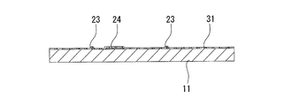
- the entire back surface of the base material 10 of the identifier providing device (that is, the entire back surface of the base portion 11 and the tab 12) is completely formed by the primary coat 31 and the secondary coat 32 as a shielding layer. Shielded by. Thereby, the whole conductive layer pattern 20 formed on the back surface of the substrate 10 is also completely shielded by the primary coat and the secondary coat as the shielding layer.
- the primary coat 31 covers the entire back surface of the base material 10 as the undercoat layer (covered with the conductive layer pattern 20 to be precise).
- the exposed portion) and the entire conductive layer pattern 20 on the base material 10 are applied and printed on the base material 10 and the conductive layer pattern 20 so as to cover the entire conductive layer pattern 20. And a lower shielding layer having the same outer shape.
- the primary coat 31 is a lattice-like or matrix-like coating film, in which a large number of rectangular openings are densely arranged at regular intervals in the vertical and horizontal directions of the substrate 10. That is, the back surface of the base material 10 and a part of the conductive layer pattern 20 are exposed from the opening of the primary coat 31.
- the primary coat 31 is formed in the above-mentioned lattice coating film shape by using blue (ultra blue, blue, etc.) printing ink.
- the secondary coat 32 has a back surface portion of the base material 10 and a conductive layer pattern on the base material 10 over the entire range of the back surface of the base material 10 as an overcoat layer or an exposed layer.
- 20 is applied by printing on the primary coat 31 so as to cover the entirety of the primary coat 31 from above, and is integrally laminated to form an upper shielding layer having the same outer shape as the outer shape of the substrate 10.
- the secondary coat 32 is a completely sealed sheet-like or film-like coating film (without gaps and openings). That is, from the secondary coat 32, the back surface of the substrate 10 and a part of the conductive layer pattern 20 are not exposed at all (via the lattice-shaped primary coat 31). The entire back surface including the conductive layer pattern 20 is completely shielded from the outside.
- the secondary coat 32 is also formed in the above-described film coating (or solid coating without pores) with the same (preferably the same) blue printing ink as the primary coating 31.
- the primary coat 31 and the secondary coat 32 are formed of blue printing ink, completely shield the silver-based conductive layer pattern 20 on the substrate 10 from the outside, and the internal conductive layer pattern. 20 is not easily visible from the outside.
- the primary coat 31 and the secondary coat 32 are formed with a blue printing ink
- the primary coat 31 has a lattice coating shape as described above and the secondary coat 32 has a film coating shape
- Efficiency hindering visual recognition of the silver-based conductive layer pattern 20 on the substrate 10 from the outside due to an optical effect (with respect to external light entering the shielding layer) due to a large number of lattices (and a large number of openings) of the primary coat 31. (Hereinafter, sometimes referred to as “visual shielding efficiency”) can be increased.
- the identifier providing device can also use white and / or gray printing ink as a shielding layer that shields the conductive layer pattern 20 on the substrate 10 from the outside.
- the primary coat as the undercoat layer of the shielding layer of another example is applied on the base material 10 and the conductive layer pattern 20 by printing so as to cover the entire area of the back surface of the base material 10 like the primary coat 31.
- they are integrally laminated to form a lower shielding layer having the same outer shape as the outer shape of the substrate 10.
- this primary coat forms gray (gray) printing ink as a completely sealed sheet-like or film-like coating film (no gaps and openings) similar to the secondary coat 32. That is, in this case, the back surface of the base material 10 and a part of the conductive layer pattern 20 are not exposed at all even from the primary coat as the undercoat layer, and the primary coat covers the entire back surface of the base material 10 with the conductive layer. The pattern 20 is completely shielded from the outside.
- the secondary coating as the overcoat layer of the shielding layer in another example is the same as the secondary coating 32, and the back surface portion of the base material 10 and the conductive layer pattern on the base material 10 over the entire back surface of the base material 10. 20 is applied by printing on the primary coat so as to cover the entire gray primary coat from above, and is integrally laminated to form an upper shielding layer having the same outer shape as that of the base material 10.
- the secondary coat is formed in the same film coating as the secondary coat 32 by white printing ink.
- the back surface of the base material 10 and a part of the conductive layer pattern 20 are not exposed at all, and the secondary coating covers the entire back surface of the base material 10 from above the primary coating.
- the conductive layer pattern 20 is completely shielded from the outside.
- the primary coat 31 and the secondary coat 32 are respectively formed of a gray-based and white-based printing ink, and completely shield the silver-based conductive layer pattern 20 on the substrate 10 from the outside.
- the internal conductive layer pattern 20 is not easily visible from the outside.
- the primary coat 31 and the secondary coat 32 are formed with a white and / or gray printing ink, the primary coat 31 is formed into a gray film coating as described above, and the secondary coat is white.
- the optical effect of the primary coat of the same color as that of the conductive layer paste 20 (with respect to the external light entering the shielding layer) and the white system that increases the gray brightness of the primary coat Due to a synergistic effect with the optical effect of the next coat, the efficiency of hindering visual recognition of the silver-based conductive layer pattern 20 on the substrate 10 from the outside (hereinafter sometimes referred to as “visual shielding efficiency”) is increased. be able to.
- the identifier providing apparatus of the present embodiment typically uses a paper material as a raw material of the base material 10, a silver paste ink as a conductive ink as a raw material of the conductive pattern 20, and a normal printing ink as a pattern portion 13. And as a raw material of the shielding layers 31 and 32, it can mass-produce using a screen printing technique.
- a base paper 100 made of a paper material constituting the base material is set on a screen printing machine (not shown) to form the next conductive pattern.
- the conductive pattern 20 is formed by printing with silver paste ink on one side of the base paper (that is, the back surface of the identifier providing device).
- the base paper 100 is divided into a plurality of lines in the width direction of the base paper 100 (vertical direction in FIG. 4A), and the length direction of the base paper 100 (left and right in FIG. 4A).
- a predetermined plurality of conductive patterns 20 are formed so as to have a plurality of rows in the direction).
- a two-dot chain line is an imaginary line (hereinafter referred to as “base”) that is a boundary line that becomes the outer peripheral edge (the outer peripheral edge of the base portion 11) of the identifier providing device (after the cutting process as the final process).
- the secondary coat forming step the entire area inside the substrate outline is covered from above each secondary coat 31 on the base paper 100 by a screen printer.
- the secondary coating 32 is formed by printing with a predetermined blue printing ink.
- the broken line in Fig.5 (a) is the outline of the inner periphery of the extension part 22 of the conductive layer pattern 20 under the secondary coat 32 (and primary coat 31), and the conduction
- each screen of the one side surface is formed on the other side surface of the base paper (that is, the surface serving as the surface of the identifier providing device) by a screen printer.
- the pattern portion 13 is formed by printing with a predetermined printing ink so as to match the material outline.
- the front side and the back side of the base paper 100 have a predetermined number of identifier providing devices on the front side of the printing unit (that is, the pattern unit 13) and the back side of the printing unit (that is, the conductive layer pattern 20, the primary coat 31, A secondary coat 32) can be formed by screen printing.
- FIG. 7 a cross-sectional view of the identifier providing device including the cross section of the conducting portion 23 and the PC-side contact portion 24
- FIG. 8 the identifier providing device including the cross section of the conducting portion 23
- FIG. 9 transverse cross section of the identifier providing device including the cross section of the conducting portion 23 and the PC side contact portion 24
- the conductive layer pattern 20 has a predetermined film thickness on the base material 10, and The layers are formed to have a predetermined wiring pattern.
- a primary coat 31 is laminated on the conductive layer pattern 20 as shown in FIGS. 7 to 10, but the above-mentioned (although not depicted in FIGS. 7 to 10) As described above, the secondary coat 32 is laminated on the primary coat 31.
- the silver paste ink that is the raw material ink for forming the conductive layer pattern 20 is obtained by dispersing the selected silver flakes 50 in a predetermined binder.
- a mixture of polyurethane resin and heat-resistant resin is used as a binder for dispersing.
- This binder is blended at a predetermined blending rate in silver pace ink as a raw material ink.
- the blending ratio of the binder is set according to the blending ratio (or content ratio) of the selected silver flakes 50 in the silver paste ink and the blending ratio (or addition ratio) of the diluent.
- the proportion of the selected silver flake 50 is an arbitrary value within the range of 30 to 45% by weight
- the proportion of the diluent is an arbitrary value within the range of 3 to 5% by weight.
- the blending ratio of the binder can be set as an arbitrary value within the range of 50 to 67% by weight.
- the identifier providing apparatus of the present invention prints the conductive layer paste 20 on the base material 10 by configuring the binder of the silver paste ink with a mixture of polyurethane resin and heat resistant resin (and In the product state in which the shielding layer is printed), even if the base material 10 is greatly bent (in an extreme case, it is bent 180 degrees), the conductive layer pattern 20 (in particular, is in an electrically connected state to each other as described later) The selected silver flake 50 and its connecting part) are not cracked or damaged, and the conductive layer pattern 20 maintains the original good conductivity. This is presumably because the conductive layer pattern 20 is given sufficient flexibility when the binder contains a polyurethane resin.
- the heat resistant resin in the binder exhibits heat resistance, and (and This is considered to be to maintain the flexibility of the polyurethane resin in the binder (which has become a product form) at a sufficient value and to improve the bending resistance of the conductive layer pattern 20 of the identifier providing device. That is, in the identifier providing device of the present invention, the binder in the silver paste ink imparts a very large bending resistance to the conductive layer pattern 20 due to the synergistic effect of the polyurethane resin and the heat resistant resin, and the conductive layer pattern 20 is disconnected. (That is, maintain a predetermined conductivity).
- the silver paste ink that is the raw material ink for forming the conductive layer pattern 20 is a conductive paste (that is, in the case of the present embodiment, The silver paste) is not diluted to a considerable dilution ratio (for example, several tens to several hundreds weight%) with a solvent, but only a very limited amount of diluent is added.
- a considerable dilution ratio for example, several tens to several hundreds weight
- a solvent for example, several tens to several hundreds weight
- the present inventors cannot obtain the desired electrical conductivity even if printing on the base paper 100 is possible, and the dilution rate is increased. It is confirmed that the conductivity decreases as the level increases, and the final conductive layer pattern 20 becomes non-conductive.
- the conductive layer pattern formed has a certain level of conductivity (conductivity), even if it can obtain a certain level of conductivity (conductivity). It is also confirmed that when the conductive layer pattern 20 of the identifier providing device of the present invention is in close contact with the capacitive touch device, sufficient capacitance cannot be obtained to drive the capacitive touch device. ing.
- the silver paste ink as a stock solution has a predetermined diluent added in a very limited amount (that is, at a very limited addition rate).
- ethylene glycol monobutyl ether also known as butyl cellosolve or buticello
- the addition rate of the diluent is a very limited (very small) addition rate in the range of 3 to 5% (% by weight).
- the conductivity of the conductive layer pattern 20 of the identifier providing device is lowered from an intended value, and the conductive layer pattern 20 is brought into close contact with the capacitive touch device. In such a case, there is a possibility that sufficient capacitance for driving the capacitive touch device cannot be obtained.
- the dilution ratio of this diluent is less than 3%, the viscosity of the silver paste ink as a stock solution is too high, and there are problems such as difficulty in printing on the base paper 100 and a decrease in mass productivity due to a decrease in printing speed. appear. With such a very small addition rate (3 to 5%), the present inventors can achieve a sufficient printing speed for mass production of the identifier providing device after manufacture and the desired conductivity of the identifier providing device. It is confirmed that both can be achieved.
- Silver paste inks generally contain silver particles (both spherical and flaky silver particles) in order to obtain a desired specific resistance (volume resistivity) of 10 ⁇ 5 ⁇ cm.
- the ratio is set in the range of 80 to 90%. If the content is lower than this, the desired specific resistance (volume resistivity) of 10 ⁇ 5 ⁇ cm cannot be obtained.
- the content of the selected silver flake 50 in the silver paste ink is set within the range of 30 to 45% (weight%). And the content rate of 30% is adopted as the minimum amount (lower limit). In consideration of variations in print quality and the like, as a safe content rate range for obtaining a desired specific resistance (volume resistivity) of 10 ⁇ 5 ⁇ cm, the content rate of the selected silver flake 50 is 40 to 45. % (% By weight) is preferable.
- the identifier providing apparatus of the present invention uses the silver paste ink having a small content of the selected silver flake 50 as described above, but the conductive layer pattern 20 manufactured using the silver paste ink has a certain conductivity.
- a ⁇ 10 ⁇ 5 ⁇ cm (where “a” is an arbitrary real number in the range of 1 to less than 10), for example, 1.0 ⁇ 10 ⁇
- the inventors have confirmed that 5 ⁇ cm or a value close to this can be obtained.
- the resistivity of bulk silver is 1.59 ⁇ 10 ⁇ 6 ⁇ cm
- the resistivity of the conductive layer pattern 20 of the identifier providing device of the present invention is the resistivity of bulk silver. It is a sufficiently good value compared to.
- the selected silver flake 50 is added to the binder having a predetermined mixing ratio made of polyurethane resin and heat-resistant resin as described above.
- a silver paste ink stock solution was prepared by blending with the above, and this silver paste ink stock solution was diluted with a predetermined diluent at a very limited dilution rate (after viscosity adjustment), using a silver paste ink Yes.
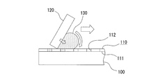
- a screen 110 having a predetermined mesh size for example, an arbitrary mesh size within a range of 100 to 500 mesh
- a mesh size screen 110 having an opening diameter through which the selected silver flake 50 having a maximum particle diameter (for example, 5 ⁇ m) passes is used.
- the screen 110 is masked by the mask portion 111 so as to form a predetermined conductive layer pattern 20. That is, the screen 110 forms a mask opening 112 corresponding to the predetermined conductive layer pattern 20 by the mask portion 111 of the screen 110.
- a squeegee 120 having a predetermined form for example, a flat shape
- a predetermined material for example, polyurethane rubber or silicon having an arbitrary hardness in the range of 60 to 90 degrees.
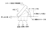
- the attack angle ⁇ 1 of the squeegee 120 is set to a predetermined angle.
- the attack angle ⁇ 1 can be set to an arbitrary value within a range of, for example, 70 degrees or less, and the silver paste ink of the present invention (including the present embodiment) having a high viscosity is applied to the mask opening 112 of the screen 110. Angles that are much smaller than 70 degrees, such as 30 to 35 degrees, 35 to 40 degrees, 40 to 45 degrees, 45 to 50 degrees, etc.
- the actual squeegee angle ⁇ 2 is set during printing in relation to the hardness of the squeegee 120 (and the elastic modulus determined depending on the hardness).
- the predetermined angle smaller than the attack angle ⁇ 1 is maintained.
- the actual squeegee angle ⁇ 2 is 30 to 30 instead of the attack angle ⁇ 1.
- a hardness of 120 may be set.
- the squeegee speed (print speed) V is set to a predetermined speed.
- the squeegee speed V can be in the range of 1 mm to 100 mm / sec.
- the balance between the two 1-5 mm / sec, 5-10 mm / sec, 10-15 mm / sec, 15-20 mm / sec, 20-25 mm / sec, 25-30 mm / sec, 30-35 mm / sec, 35-40 mm / sec, 40- The range can be 45 mm / sec or 45 to 50 mm / sec.
- raw material ink 130 made of silver paste ink is filled while rolling into the mask opening 112 of the screen 110 as the squeegee 120 moves.
- the raw material ink 130 rolls on the mask opening 112 from the position immediately before the mask opening 112 of the screen 110 (the position of FIG. 14A), It contacts the inner wall surface of the mask opening 112 and is filled from the inner wall surface portion by the contact resistance (that is, filling is started from the section 1L1 in FIG. 15).
- the raw material ink 130 rolls further on the mask opening 112 and is sequentially filled in place of the back side of the mask opening of the screen 110 in FIG.
- the raw material ink 130 is rolled (rolled) on the mask opening 112 to reduce its viscosity (due to its thixotropy), so that the raw material ink 130 can be easily and smoothly filled into the mask opening 112. Will be done.
- the squeegee speed V and the raw material ink height H are divided into sections. This greatly affects the filling efficiency of the raw material ink 130 into 1L1.
- the squeegee speed V, the attack angle ⁇ 1, and the actual squeegee angle ⁇ 2 greatly affect the filling efficiency of the raw material ink 130 into the section 3L3.
- the pressing amount st (determined by the printing pressure F and the flexibility of the screen 110 itself) and the printing pressure F are the section. It affects the filling efficiency of the raw material ink 130 into 2L2. Therefore, in the present invention (including this embodiment), in order to perform the ink filling operation in the section 1L1, the section 2L2, and the section 3L3 in the mask opening 112 of the screen 110 uniformly and efficiently, the sections L1, L2, Parameters such as the squeegee speed V, the attack angle ⁇ 1, and the actual squeegee angle ⁇ 2 at L3 are set to optimum values.
- the raw material ink 130 is filled in each mask opening 112 of the screen 110 while rolling, It is printed on the printing surface of the base paper 110 under the screen 110.
- the raw material ink 130 in the mask opening 112 of the screen 110 is in contact with the wall surface of the mask opening 112.
- the shear deformation portion 131 is generated by the shear stress in the shear direction between the two. Therefore, the raw material ink 130 is smoothly discharged from the mask opening 112 due to a decrease in viscosity (due to thixotropy) due to the shear deformation force in the shear deformation portion 131, and is printed on the surface of the base paper 100 as the conductive layer 20A. .
- the conductive layer 20A is printed in a predetermined pattern on the surface of the base paper 100. Finally, a predetermined pattern shape is formed on the base paper 100. The conductive layer pattern 20 is formed.
- the linear conductive portion 23 of the conductive layer pattern 20 is arranged in the length direction of the base paper 100 shown in FIG.
- the screen 110 is masked by the mask portion 111 so that the length directions coincide with each other to form a mask opening 112, and screen printing is performed by the screen 110.
- the moving direction of the squeegee 120 and the length direction of the conductive portion 23 portion of the mask opening 112 of the screen 110 coincide with each other. Can be printed with quality.
- the identifier providing device of the present embodiment is a silver flake made of scale-like, flake-like or flaky silver particles as shown in FIG. 12A as silver particles of the silver paste forming the conductive layer pattern 20.
- the selected silver flakes 50 prepared and / or selected to have a uniform particle size with a minimum thickness are used.
- the outer contour of the selected silver flake 50 shown in the figure is schematic, and the actual selected silver flake 50 has a scaly shape that has various outer contours and does not have a constant shape, as with normal silver flakes. It has become.
- the sorted silver flakes 50 are substantially 100% silver (pure silver) flaky particles (excluding impurities).
- these metal materials have characteristics equivalent to the pure silver flake 50 made of pure silver according to the present embodiment (mainly due to its thickness. It is difficult to obtain characteristics. That is, since pure silver has good malleability / ductility (after gold), the average thickness required for the conductive layer pattern 20 of the present invention is secured as a predetermined thickness (typically, an average thickness of about 50 nm) described later. An effect peculiar to the conductive layer pattern 20 of the present invention, which will be described later, can be exhibited. However, in other metal materials (excluding gold), the minimum thickness that requires the average thickness required for the conductive layer pattern 20 of the present invention. Can not be secured as.
- gold is more preferable than silver because it is more malleable / ductile than silver, but it is more preferable than the average thickness.
- gold is considerably more expensive than silver, so it is still necessary to use silver from the viewpoint of cost. Is preferred.
- the silver flakes forming the conductive layer pattern 20 of the identifier providing device of the present invention and the present embodiment have a predetermined small thickness and a substantially uniform particle size (very limited particle size range). It consists only of the selected silver flakes 50 prepared and / or sorted so as to have no silver particles other than the selected silver flakes 50.
- the selected silver flake 50 has an average thickness measured by observation with a scanning electron microscope (SEM), for example, which is the predetermined thickness (typically about 50 nm).
- the selected silver flake 50 having an average thickness of about 50 nm.
- 50 nm as the average thickness of the selected silver flakes 50 is very difficult to measure the thickness of one of the selected silver flakes 50 having such a very small thickness.
- the total thickness of the aggregate of the predetermined number (for example, 10) of the selected silver flakes 50 is measured by, for example, SEM observation, and the total thickness is the predetermined number.
- each of the selected silver flakes 50 has an average thickness of about 50 nm as a typical example of the predetermined average thickness. In some cases, 50 nm is practically used, such as a range of 50 nm to 60 nm, a range of 50 nm to 55 nm, or the like. In some cases, the average thickness has a predetermined range having a certain width above as a lower limit. Moreover, as shown in FIG.12 (b), each selection silver flake 50 is not necessarily the whole thickness including the center part and edge part uniformly, but according to a site
- the maximum thickness portion of the maximum thickness T1 is larger than the average thickness (about 50 nm) of the selected silver flakes 50, for example, about 100 nm at maximum (typically within a range of 50 nm to 100 nm).
- the minimum thickness T3 is smaller than the average thickness, for example, a minimum of about 25 nm (typically within a range of 30 to 50 nm, and a minimum is 20 to 40 nm, 25 nm to 35 nm, or Within the range of 20 nm to 30 nm).
- the minimum thickness portion of the minimum thickness T3 basically exists at the outer peripheral edge portion of the selected silver flake 50 as a minimum thickness portion, but is a portion closer to the center than the outer peripheral edge portion (in the extreme case, the central portion). It may be present in FIG. 12B is an explanatory diagram for schematically showing the thickness distribution of the selected silver flakes 50. For convenience of description, the central position of the selected silver flakes 50 is defined as the maximum thickness T1.
- the portion near the outer peripheral edge is set as the minimum thickness T3, and the portion at the intermediate position between the central position and the position near the outer peripheral edge is drawn as the intermediate thickness T2.
- the thickness T2 and the minimum thickness T3 are not necessarily present at the central position, the intermediate position, and the position near the outer peripheral edge, but may be present at different positions.
- the “partial melting” means that at least the “minimal thickness portion of the selected silver flake 50 is in a molten state” (that is, other thicker portions are not basically in a “melted” state). It is used in the meaning of. That is, the first heating temperature range is a temperature range in which at least the minimum thickness portion of the selected silver flake 50 is in a molten state (that is, in a “partial molten” state), and the lower limit is about 200 ° C. Typically, the upper limit is set to about 300 ° C., a temperature range of about 200 ° C. to about 300 ° C., a temperature range of about 200 ° C. to about 250 ° C., and a temperature of about 200 ° C.
- the first heating temperature range may be referred to as a “partial melting temperature range” for convenience of explanation.
- the partial melting temperature range in the temperature range of less than about 230 ° C. (that is, the temperature range of about 200 ° C.
- the portion where the “partial melting” state does not occur in the minimum thickness portion of the selected silver flake 50
- the present inventors have confirmed through experiments and the like that there is a possibility that there is a certain amount, but in a temperature range where the lower limit is about 230 ° C. (that is, a temperature range of about 230 ° C. or higher)
- the ratio at which the minimum thickness portion of the silver flake 50 is in the “partially melted” state can be greatly increased.
- sorting is performed in the temperature range where the lower limit is about 250 ° C. (that is, the temperature range of about 250 ° C. or more).
- the present inventors have confirmed through experiments and the like that the ratio at which the minimum thickness portion of the silver flake 50 is in the “partially melted” state can be made substantially 100% or 100%.
- the adjacent selected silver flakes 50 in the silver paste of the raw material ink 130 applied to the base paper 100 are partially melted at least in the minimum thickness portion by heating in the partial melting temperature range, and the minimum Electrical conductivity (and specific resistance characteristics) between the selected silver flakes 50 arranged adjacent to each other through the welded portions (partial welded portions) between the minimum thickness portions that are partially welded in the thickened portions (partial welded portions). ), And finally, the specific resistance of the conductive layer pattern 20 in a state where a large number of selected silver flakes 50 are laminated becomes a desired specific resistance value (specific resistance value on the order of 10 ⁇ 5 ⁇ cm). I am doing so.
- the minimum thickness portion of the selected silver flake 50 is typically the minimum thickness portion of the minimum thickness T3, and in addition to this, the intermediate thickness portion or a portion between the intermediate thickness portion and the minimum thickness portion.
- the portion where the thickness is 50 nm or less, and the portion where the thickness is 50 nm or less between the intermediate thickness portion and the maximum thickness portion are also the minimum thickness portions.
- the selected silver flake 50 of the present invention may be heated even in a predetermined second heating temperature range that is lower than the first heating temperature range.
- the minimum thickness portion is in a softened state (although it does not become the “partially molten” state) or in a state approaching the molten state, and the selected silver flakes 50 arranged adjacent to each other in the silver paste have at least their minimum thickness portions. And softened and deformed to cause partial aggregation (partial aggregation) at the minimum thickness portion, and between the adjacent silver flakes 50 arranged adjacent to each other via the aggregation portion (partial aggregation portion) between the minimum thickness portions.
- the electrical conductivity (and resistivity characteristics) are greatly improved (although lower than the above-mentioned “partial welding”), and finally the conductive layer pattern 20 in a state where a large number of selected silver flakes 50 are laminated.
- Resistivity Functions to reach the desired resistivity (10 -5 [Omega] cm resistivity of the order).
- the second heating temperature range is a temperature range in which at least the minimum thickness portion of the selected silver flake 50 is in a softened aggregate state (that is, a “partial aggregate” state), and an upper limit value thereof is less than 200 ° C.
- the second heating temperature range is another temperature range such as a temperature range of about 150 ° C. to about 200 ° C., a temperature range of about 150 ° C. to about 180 ° C., a temperature range of about 80 ° C. to about 130 ° C.
- the second heating temperature range may be referred to as a “partial aggregation temperature range” for convenience of explanation.
- all the portions of the selected silver flake 50 having a thickness in the range of 25 nm to 35 nm, 20 nm to 30 nm, or 20 nm to 35 nm (hereinafter, sometimes referred to as “ultra-minimal thickness portion”).
- the ultra-small thickness portion between the selected silver flakes 50 that are in a laminated state and are in contact with each other or in close contact with each other is more reliably partially melted in the partial melting temperature range (or
- One of the main features is to achieve welding between these ultra-minimum thickness portions by completely melting the ultra-minimum thickness portions.
- the ultra-minimum thickness portion of the selected silver flake 50 is typically the minimum thickness portion of the minimum thickness T3. However, as in the case of the minimum thickness portion, in addition to this, therefore, it is considered that there is no possibility that the intermediate thickness part and other parts become the ultra-small thickness part.
- the selected silver flake 50 of the silver paste forming the conductive layer pattern 20 has a very small particle diameter measured by, for example, observation with a scanning electron microscope (SEM) and a very limited particle size range (typical Is composed only of silver flakes that fit within a small particle size range of about 3.5 to about 4.5 ⁇ m (hereinafter sometimes referred to as “minimum limited particle size range”). No silver flakes other than the particle size range are contained at all, and only selected silver flakes 50 in the extremely limited particle size range (that is, a very small particle size and a very narrow particle size distribution) are used as silver particles. in use.
- SEM scanning electron microscope
- silver flakes generally have a certain particle size distribution as a product form after production, and the particle size distribution usually has a particle size distribution in the range of at least several ⁇ m (a variation of at least 3 ⁇ m or more or 4 ⁇ m or more).
- the present invention classifies silver flakes having such a particle size distribution and sorts the particle size, and selectively uses only silver flakes with a limited particle size within a predetermined range to constitute sorted silver flakes 50,
- the conductive layer pattern 50 is formed using a silver paste prepared only with the selected silver flakes 50 in the limited particle size range.
- the selected silver flake 50 (not shown) is a silver paste that is included in a very narrow particle size range (typically within a particle size range of about 1 ⁇ m) in the particle size distribution graph.
- the particle size distribution graph has very sharp rising and falling particle size distributions (specifically, in the case of the above limited particle size range, the particle size “3.5 ⁇ m” It has a particle size distribution that suddenly rises almost vertically from the vicinity and suddenly falls almost vertically in the vicinity of the particle diameter “4.5 ⁇ m”).
- the particle size of the selected silver flake 50 having such a limited particle size range can be confirmed by using, for example, measurement results obtained by a laser diffraction / scattering particle size / particle size distribution measurement method.
- the particle size of the selected silver flake 50 of the present invention is preferably in the range of about 3.5 to about 4.5 ⁇ m as described above, but besides this, the above-mentioned limited particle size range (about 1 ⁇ m) is preferable.
- the particle diameter is within the range, for example, the particle diameter is in the range of 3.0 to 4.0, and the particle diameter is in the range of 4.0 to 4.5 ⁇ m. It is also possible. However, from a practical point of view including limitations on the production technology of silver flakes, it is desirable that the particle size of the selected silver flakes 50 is in the range of about 3.5 to about 4.5 ⁇ m as described above.
- the selected silver flake 50 of the silver paste has a median value (4.0 ⁇ m) to a maximum value (4.0 ⁇ m) in the particle size range (3.5 to 4.5 ⁇ m).
- this point is also one of the features of the present invention from the viewpoint of obtaining the above-mentioned specific effects (realization of fine printing, etc.).
- the selected silver flakes 50 forming the layer pattern 20 have a very small particle size of about 3.5 ⁇ m to about 4.5 ⁇ m as described above, the particle size range thereof is the above-mentioned (about 1 ⁇ m range)
- Such a selected silver flake 50 is regarded as an aggregate of silver flakes having a substantially uniform particle size with the above-mentioned extremely small particle size (about 3.5 ⁇ m to about 4.5 ⁇ m). Can do. Since the selected silver flake 50 has a small particle size and a uniform particle size range, it is contained in a silver paste together with a binder and screen-printed on the substrate 10 in the conductive layer forming step of the conductive layer pattern 20.
- the content of the selected silver flakes in the silver paste is set to a predetermined content (substantially lower than the content of silver particles in the conventional silver paste), as described later, All of the selected silver flakes contained in the silver paste are contained inside the silver paste layer printed and formed on the base material 10 (that is, the content rate does not decrease).
- the original content of silver flakes in the conductive layer it is possible to maintain the packing density of the selected silver flakes 50 in the conductive layer at a predetermined density. Can be demonstrated.
- a screen having a large mesh number is used to perform fine printing, for example, when the conductive portion 23 of the conductive layer pattern 20 has a fine width (that is, the diameter of the mask opening of the screen is very large).
- the selected silver flakes 50 smoothly pass through the mask opening of the screen in the same manner as the spherical silver particles, even in the case of having a scale-like outer shape.
- the original content of the silver flakes in the silver paste to be formed can be maintained, the packing density of the selected silver flakes 50 in the conductive layer can be maintained at a predetermined density, and a very fine pattern as the conductive layer pattern 20 Printing becomes possible.
- the silver paste forming the conductive layer pattern 20 contains the selected silver flakes 50 at a predetermined content, but has a sufficiently excellent specific resistance as described above. While achieving (10 -5 ⁇ cm), its content is significantly reduced compared to conventional silver paste, reducing raw material costs (by reducing the relative amount of expensive silver used) It contributes to. Specifically, in the case of using, for example, spherical silver particles, the conventional silver paste needs to have a silver particle content of 80 to 90% in order to obtain a specific resistance of 10 ⁇ 5 ⁇ cm level. is there.
- the silver paste has a content of the selected silver flake 50 in the range of 30 to 45% (% by weight), but has a specific resistance of 10 ⁇ 5 ⁇ cm level.
- the selected silver flakes 50 have the minimum particle size and the limited particle size range as described above, and reliably maintain a predetermined content (and filling rate) in the conductive layer on the screen-printed substrate 10.
- a partial welded portion (and / or the partial aggregated portion depending on the temperature range) between adjacent selected silver flakes 50, as described later.
- the specific resistance of the conductive layer formed by the partially welded portion is drastically improved. Therefore, even if the silver flake content is significantly less than the conventional, It is considered that this is because the conductive layer can ensure a desired specific resistance.
- the content of the selected silver flakes 50 in the silver paste can be 30% (by weight) (as the minimum required amount or the lower limit), or 30 to 35%, 35 to 40 %, A range of 40 to 45%, etc., or any value within these ranges.
- the content of the selected silver flakes 50 in the silver paste is in the range of 40 to 45% in order to reliably obtain a desired specific resistance (specific resistance of at least 10 ⁇ 5 ⁇ cm level) in the formed conductive layer, or
- the value is preferably set to any value within the range (for example, 40% or 45%).
- the silver paste SP which is the raw material of the conductive layer pattern 20 contains the selected silver flakes 50 dispersed in the binder 60 at the predetermined content, and the screen In a state immediately after printing on the base paper 100 by printing (before heating and drying), a layer or film having a predetermined thickness is formed. Note that when the silver paste is printed on the base paper 100 via the screen by screen printing, the selected silver flakes 50 dispersed in the binder 60 are changed in the posture in the binder 60 due to their own scale shape and the like.
- the binder 60 As shown in (c), they are oriented in the binder 60 so as to be substantially parallel to each other. Then, when the layer of the silver paste SP on the base paper 100 is heated and dried, the volatile matter of the binder 60 (and the diluent when the silver paste SP contains the diluent) is volatilized, and the conductive layer of the conductive layer pattern 20 Form.
- the conductive layer is in the form of a thin film having the predetermined thickness and comprising the solid content of the binder and the selected silver flakes 50. At this time, in the conductive layer, adjacent sorted silver flakes 50 overlap at least partly due to shrinkage stress accompanying solidification shrinkage of the binder 60 (by heating or the like), and are in surface contact with each other at the overlapped part. Conduct.
- adjacent silver flakes 50 adjacent to each other are brought close to each other by contraction stress accompanying solidification shrinkage of the binder 60 (but not close to each other), and the solid content of the binder 60 is sandwiched between them.
- electrical conduction is ensured by the dielectric breakdown of the binder 60 between the adjacent selected silver flakes 50.
- the silver paste SP on the base paper 100 is heat-treated to form a conductive layer pattern 20 as a final conductive layer.
- the selected silver flakes 50 inside the conductive layer pattern 20 are: As described above, it has a thickness from the maximum thickness T1 to the minimum thickness T3.
- the selected silver flakes 50 inside the conductive layer pattern 20 are at least partially welded by heat treatment in the partial melting temperature region in the heating and drying step after screen printing at least in the minimum thickness portion where the thickness is 50 nm or less. Alternatively, they are fused (or at least partially aggregated by heat treatment in the partial aggregation temperature range).
- the silver paste SP on the base paper 100 is heated for a predetermined time at a heating temperature in a predetermined partial melting temperature range.
- the heating temperature in this heating and drying step is preferably lower than the temperature at which the base material 10 starts to change quality by heating during the heating and drying step (hereinafter sometimes referred to as “altering start temperature”) (below the change starting temperature). Temperature).
- altering start temperature the temperature at which the base material 10 starts to change quality by heating during the heating and drying step
- Temperature temperature at a paper material is used as the base material 10
- the temperature is set to a temperature range sufficiently lower than the ignition temperature or ignition point of the paper material.
- the ignition point is 450 ° C., for example, the temperature is less than 230 ° C., preferably less than 200 ° C., or less than 180 ° C.
- the heating temperature can be in the temperature range of 180 to 230 ° C., 180 to 220 ° C., 180 to 210 ° C., 180 to 200 ° C., or 180 to 190 ° C.
- the heating temperature may be a temperature range of 150 to 180 ° C., 150 to 170 ° C., or 150 to 160 ° C. as a lower temperature range.
- first low temperature region the temperature at which moisture in the paper material does not scatter (that is, in the case of an atmosphere of 1 atm, a temperature lower than 100 ° C., hereinafter referred to as “first low temperature region”).
- the heating temperature can be a temperature range of 70 to 90 ° C. or 75 to 85 ° C., or a temperature range of 75 to 80 ° C. or 80 to 85 ° C.
- a predetermined heating temperature in the heat drying step is set as a predetermined temperature within the partial melting temperature range.
- the selected silver flakes 50 are overlapped in the conductive layer 20 ⁇ / b> A printed on the base paper 100 in a state of being substantially parallel to each other.
- the sorting is performed.
- the silver flakes 50 will overlap each other (basically with a binder component in between), typically at their respective peripheries.
- the minimum thickness portion or the ultraminimum thickness portion of each of the selected silver flakes 50 is the minimum thickness (thickness of 50 nm or less) or the ultraminimum thickness (thickness of 25 to 35 nm, etc.) such as the minimum thickness T3, respectively.
- the minimum thickness T3 is the minimum thickness (thickness of 50 nm or less) or the ultraminimum thickness (thickness of 25 to 35 nm, etc.) such as the minimum thickness T3, respectively.
- a predetermined temperature within the partial melting temperature range hereinafter, sometimes referred to as a “relatively low temperature range” in the sense of a heating temperature range of a silver paste that is relatively lower than the conventional temperature.
- the present inventors have confirmed that a partially molten state is obtained. In this case, as shown in FIG.
- the volatile components of the binder evaporate with heating in the relatively low temperature region, and the adjacent selected silver flakes 50 are in close contact with each other.
- Opposing minimum thickness portions or super minimum thickness portions are melted and fused together to form a fused portion 52.
- portions other than the minimum thickness portion or the ultra-minimal thickness portion of the selected silver flakes 50 (the selected silver flakes 50 are not melted, but are softened and deformed by heat, etc.) It is considered that the contact portion 51 is in close contact with the surface.
- a large electrical conductivity can be obtained between the adjacent selected silver flakes 50, particularly via the fused portion 52, and a good electrical conductivity can be obtained also in the close contact portion 51.
- the resin component (solid content) of the binder remains between the selected silver flakes 50.
- the interval between the selected silver flakes 50 is (several In this case, the resin component of the binder between the selected silver flakes 50 breaks down, and the electrical conductivity can still be secured. It is done.
- the minimum thickness portion or the ultraminimum thickness portion of each of the selected silver flakes 50 is the minimum thickness (thickness of 50 nm or less) such as the minimum thickness T3 or the ultrathin thickness (thickness of 25 to 35 nm, etc.).
- the present inventors have confirmed that even in the relative low temperature range, the melt is caused by the size effect.
- the volatile components of the binder evaporate along with the heating in the relatively low temperature region, and the adjacent sorted silver flakes 50 are in close contact with each other. Opposing minimum thickness portions or super minimum thickness portions are melted and fused together to form a fused portion 52.
- parts other than the minimum thickness part or the ultra-minimum thickness part of the selected silver flakes 50 are close contact parts 51 in which the surfaces are in close contact with each other.
- large electrical conductivity can be obtained between the adjacent selected silver flakes 50, particularly via the fused portion 52, and good electrical conductivity can be obtained also in the close contact portion 51.
- the minimum thickness portion or the ultra minimum thickness portion overlaps each other (basically with the binder component in between) at each peripheral portion. Therefore, also in this case, the minimum thickness portion or the ultraminimum thickness portion of each of the selected silver flakes 50 is the minimum thickness (thickness of 50 nm or less) such as the minimum thickness T3 or the ultrathin thickness (thickness of 25 to 35 nm, etc.).
- the present inventors have confirmed that even in the relative low temperature range, the melt is caused by the size effect. In this case, as shown in FIG.
- the volatile components of the binder evaporate along with the heating in the relatively low temperature region, and the adjacent sorted silver flakes 50 are in close contact with each other. Opposing minimum thickness portions or super minimum thickness portions are melted and fused together to form a fused portion 52.
- parts other than the minimum thickness part or the ultra-minimum thickness part of the selected silver flakes 50 are close contact parts 51 in which the surfaces are in close contact with each other.
- large electrical conductivity can be obtained between the adjacent selected silver flakes 50, particularly via the fused portion 52, and good electrical conductivity can be obtained also in the close contact portion 51.
- the selected silver flake 50 as the silver particle component of the silver paste ink is substantially 100% silver (pure silver) (excluding impurities).
- the fine average thickness is maintained by the good malleability and ductility, and the minimum thickness and the ultra-minimum thickness are secured. Therefore, the selected silver flake 50 is particularly at the minimum thickness portion and the ultra-minimum thickness portion. , At least partially melt at a temperature within a predetermined relative low temperature range (due to the so-called size effect).
- the selected silver flakes 50 start to melt as a whole at a temperature equal to or higher than the lower limit of the relative low temperature range, for example, about 200 ° C. At this temperature, the entire sorted silver flake 50 is completely melted.
- ⁇ Thickness of conductive layer> In the identifier providing apparatus according to the present invention (including the present embodiment), in the screen printing process, silver is used so that the thickness of the conductive layer pattern 20 is in the range of 5 ⁇ m to 6 ⁇ m in the final state after printing and heating.
- the coating thickness of paste ink is set.
- a conductive layer using a conventional silver paste does not operate unless the thickness of the conductive layer is not less than a predetermined thickness. That is, it is said that sufficient conductivity cannot be obtained unless the aspect ratio (thickness / width) of the conductive layer is a large value such as about 1: 1.
- the thickness of the conductive layer is required to be at least about 10 ⁇ m.
- the average thickness of the conductive layer pattern 20 is about 5 ⁇ m (or 5 to 6 ⁇ m), which is about half of the conventional minimum value of 10 ⁇ m. Range).
- the average thickness of the conductive layer pattern 20 can be made smaller, such as in the range of 1 to 2 ⁇ m and in the range of 1 to 3 ⁇ m.
- the average thickness of the conductive layer pattern 20 is 5 to 6 ⁇ m, the inside thereof is typically several tens to hundreds of layers (calculated from the average thickness of the selected silver flakes 50) in the thickness direction.
- the sorted silver flakes 50 that are less than the layer are in a partially fused state (and the other portions are in close contact) and are stacked on each other. Even when the average thickness of the conductive layer pattern 20 is 1 ⁇ m, about 10 or more layers (or about 10 to 20 layers) of selected silver flakes 50 are partially fused in the thickness direction ( And other portions are in close contact with each other) and are stacked on each other. Although the present inventors have confirmed that sufficient conductivity can be obtained even in the conductive layer pattern 20 having such a very small average thickness, as described above, the selected silver flakes 50 It is considered that it is highly dependent on being fused at least partially (forming the fused portion 52).
- the conductive layer pattern 20 has an extremely small average thickness (for example, 5 ⁇ m to 6 ⁇ m).
- a shielding layer primary coat and secondary coat
- the first layer is primary coated with the mesh-like blue ink as described above. If the second layer is 31 and the secondary coating is made of blue solid ink, the shielding effect can be improved.
- the shielding layer is formed by printing with white ink and the conductive layer pattern 20 on the base material 10 is shielded from the outside, it is possible to use only one layer of shielding layer. In order to shield reliably, it is preferable that the shielding layer has a two-layer structure. In this case, it is not necessary to make the first layer mesh like the case of blue ink.
- the average thickness of the conductive layer pattern 20 becomes 10 ⁇ m, it becomes about twice (5-6 ⁇ m of the average thickness of the present invention).
- the contour will protrude in a convex shape, making it impossible to shield with printing ink. Therefore, in this case, a thicker shielding film or shielding sheet needs to be applied from above the conductive layer pattern 20 of the base material 10 to conceal the conductive layer pattern 20 from the outside, and work efficiency is greatly reduced. Manufacturing costs increase significantly.
- the conductive layer pattern 20 (presenting silver color) of the substrate 10 is shielded by printing with white ink
- a gray ink of the same color is applied on the conductive layer pattern 20 exhibiting silver color.
- the first shielding layer can be applied to form a second shielding layer by printing a white ink on the first shielding layer.
- the white ink layer of the second shielding layer can be formed.
- the gray color of the first shielding layer may be transmitted, and the entire back surface of the substrate 10 (surface on which the conductive layer pattern 20 is formed) may appear gray.
- a white layer is further applied as the third shielding layer, and the entire back surface of the base material 10 (surface on which the conductive layer pattern 20 is formed) is made white. Designability can also be improved. Furthermore, when a transparent protective film is applied and formed on the second shielding layer or the third shielding layer with a varnish or the like, peeling of the shielding layer can be effectively prevented. Since the cost increases, such a transparent protective film is formed (when the cost is appropriate) according to the use of the identifier providing device.
- the identifier providing apparatus of the present invention (including this embodiment) completely shields (blindfolds) with the printing ink when it is necessary to shield (blind) the conductive layer pattern 20 of the substrate 10 from the outside. Therefore, the manufacturing cost can be greatly reduced as compared with the case where a shielding film, a shielding paper, or the like is attached and shielded.
- the conductive layer pattern 20 of the base material 10 is shielded (blindfolded), if the number of shielding layers by printing is increased too much, the manufacturing cost also increases correspondingly, and the appearance of the identifier providing device Zenda Since the influence cannot be neglected, it is preferable to blindfold (shield with 2 to 3 layers) several times.
- the conductive layer pattern 20 of the substrate 10 can be completely blinded by laminating by printing with printing ink once or twice.
- the printing ink layer (first coat 31, second coat, etc.) as a shielding layer
- the printing ink is on the conductive layer pattern 20 of the substrate 10 at a level of several tens to several hundreds of nanometers or several microns. It is thought that this is because it is formed by coating. That is, when the thickness of the conductive layer is large as in the prior art, the contour of the conductive layer inevitably appears to the outside. Therefore, the smaller the thickness of the conductive layer, the more advantageous when shielding from the outside.
- the average thickness is about 30 ⁇ m, and even if the thick conductive layer is shielded with printing ink to be blinded, it cannot be completely blinded. .
- a predetermined small amount (for example, about 2%) of silicon particles is further added to the printing ink as the shielding layer of the conductive layer pattern 20 of the substrate 10. can do.
- the shielding layer is formed with this printing ink, the light passing through the shielding layer is irregularly reflected by the silicon particles dispersed inside the shielding layer, and the shielding effect can be further improved. That is, as described above, in order to shield the conductive layer pattern 20 of the base material 10 from the outside and make it difficult to see, it is better to increase the number of shielding layers of the printing ink (for example, preferably 5 to 6 layers).
- the cost is high. Therefore, instead of increasing the number of shielding layers, a predetermined small amount of silicon particles are added to the printing ink for the shielding layer, and the diffused light reflection effect is utilized.
- the present inventors have confirmed that visual recognition from the outside of the conductive layer pattern 20 can be completely suppressed by adding 2% silicon particles to the blue ink for the first coat 31 described above.
- the electrical reaction Is likely to worsen.
- the ratio of silicon particles added to the printing ink for shielding is preferably a small amount in the range of 1 to 3% by weight, and more preferably 2% by weight.
- the proportion of silicon particles added to the printing ink for shielding can be 1 to 2% by weight. However, as the proportion approaches 1%, the effect of diffused light reflection becomes small. A value close to 2% is preferable.
- the size of the conductive layer pattern 20 in the surface direction is, for example, a width of the conductive portion 23 of 1 mm and a diameter of the PC side contact portion 24 of 7 mm. be able to.
- all necessary conductive layers can be mass-produced by a printing technique (such as screen printing).
- a printing technique such as screen printing
- a technique for forming a conductive layer by printing a conductive paste containing a conventional silver paste on a base material (such as paper) hereinafter, sometimes referred to as “conventional conductive layer forming technique on a base material”.
- the conductive layer may not react sufficiently (that is, the conductive layer is not energized).
- the inventors have confirmed. This is because when the conductive layer is printed on the base material by silver paste or the like, the conductive layer on the base material is uneven, or it is difficult to deposit ink on the screen. This is probably because there was a problem. For example, when the conductive layer is uneven, the reactivity of the conductive layer is reduced and the yield is reduced. Furthermore, when forming an electroconductive layer on a base material by printing, the kneading
- the present invention solves these problems in printing technology and enables mass production.
- the present invention for example, dramatically improves the conductivity of the conductive layer pattern 20 so that the PC-side contact portion 24 has a very small diameter of 7 mm. A sufficient change in capacitance can be obtained.
- the identifier providing apparatus of the present invention can use other printing techniques in addition to using the screen printing technique as described above, for example, the gravure printing technique. It can also be used.
- the average thickness of the conductive layer pattern 20 formed on the substrate 10 can be made smaller than that in the case of screen printing (the above average thickness of 5 to 6 ⁇ m) (for example, the average thickness can be 1 ⁇ m). .)
- the particle size of the selected silver flakes 50 is in the range of 3.5 to 4.5 ⁇ m as in the case of screen printing so that the filling rate of the selected silver flakes 50 in each cell is in the range of 10 to 20. It is preferable to be inside.
- the user grips the tab 12 as a gripping portion of the base material 10 by hand, and the back surface of the base portion 11 (the surface facing the touch panel of the touch computer device).
- the PC-side contact portions 24 are in surface contact with the corresponding contact areas of the touch panel, and the plurality of PC-side contact portions 24 are connected to the touch panel (a plurality of pre-selected As a contact area) (at the same time or with a slight time lag).
- the user's finger and the selected plurality of buttons on the touch panel are: Electrical connection (electrical conduction) is made through the conductive portion 23.
- Electrical connection electrical conduction
- the electric charge moves between the user's finger and the button on which the PC-side contact portion 24 contacts, the button capacitance changes, and a unique process set in advance corresponding to the combination of the buttons Is executed by the touch-type computer device.
- the present invention can be embodied as the identifier providing apparatus of the embodiment (Embodiment 2) shown in FIG.
- the identifier providing device includes a base material 210 that is integrally formed to have a predetermined shape, and a conductive layer pattern 220 that is integrally formed within a predetermined range of the surface of the base material 210.
- the base member 210 is formed as a whole in the form of a single sheet and has a vertically long rectangular shape.
- the base portion 211 is a rectangular portion that is a main portion on one end side in the length direction, and is the remaining portion. A rectangular portion on the other end side in the length direction is used as the grip portion 212.
- the base material 210 is integrally formed of a single sheet of predetermined paper quality so as to have a sheet shape (shown in FIG. 19) including the base portion 211 and the grip portion 212.
- the conductive layer pattern 220 includes a finger contact part 221 as a human body side grounding part, an extension part 222 as a general-purpose conductor part, a conduction part 223 as an individual conductor part, and a PC side contact part 224 as a PC drive part.
- the conductive layer pattern 220 becomes a predetermined pattern on the back surface of the base portion 211 of the base 210 using slurry-like silver paste ink containing predetermined selected silver flakes. It is formed by coating.
- the finger contact portion 221 is a conductive layer having a predetermined film thickness that is applied and formed on the entire back surface of the grip portion 212, similar to the finger contact portion 21 on the back surface of the tab 12 of the first embodiment. This is a part that operates in the same manner as the unit 21 and is electrically connected to the user's finger when the user grips the grip 221 with the finger.
- the conduction unit 222 has the same configuration as the conduction unit 23 of the first embodiment and operates in the same manner as the conduction unit 23.
- the PC side contact portion 223 has the same configuration as the PC side contact portion 24 of the first embodiment, and operates in the same manner as the PC side contact portion 24.
- the conductive portion 222 and the PC-side contact portion 223 are applied and formed in a predetermined arrangement manner at predetermined positions and predetermined portions on the back surface of the base portion 211 (the same film thickness as the finger contact portion 212).
- the conductive layer has a predetermined thickness.
- the length of the base portion 211 of the substrate 210 is, for example, about 60 to 90% of the entire length of the substrate 210, preferably about 60 to 80%, more preferably
- the length of the grip 212 is, for example, about 10-40% of the total length of the substrate 210, preferably about 20-40%.
- the conductive layer pattern 220 is formed in the same manner as in the first embodiment using the same raw material ink as that of the conductive layer pattern 20 in the first embodiment.
- the identifier providing apparatus of the second embodiment can be manufactured in the same manner as the identifier providing apparatus of the first embodiment, and exhibits the same operations and effects as the identifier providing apparatus of the first embodiment.
- the present invention can be embodied as an identifier providing apparatus of the embodiment (Embodiment 3) shown in FIG.
- the identifier providing device includes a base material 310 that is integrally formed to have a predetermined shape, and a conductive layer pattern 320 that is integrally formed within a predetermined range of the surface of the base material 310.
- the base material 310 is formed as an integral sheet as a whole, has a vertically long fan shape or a rounded isosceles triangular shape, and has a substantially trapezoidal portion which is a main portion on one end side in the length direction as a base portion.
- the base material 310 is integrally formed so as to have a sheet shape (shown in FIG. 20) composed of the base portion 311 and the grip portion 312 by a single sheet of paper having a predetermined paper quality.
- the surface of the grip portion 312 is a pattern portion 313 similar to the pattern portion 13 of the first embodiment.
- FIG. 20A shows the configuration of the back side of the identifier providing device, but for convenience of explanation, a state in which no shielding layer is provided on the back surface of the substrate 310 (that is, the conductive layer pattern 320 is exposed). Is drawn). That is, the back surface of the substrate 310 is covered with the same shielding layer as that in the first embodiment after the conductive layer pattern 320 is formed.
- the conductive layer pattern 320 includes a finger contact portion 321 as a human body side grounding portion, an extended portion 322 as a general-purpose conductor portion, a conduction portion 323 as an individual conductor portion, and a PC side contact portion 324 as a PC drive portion.
- the conductive layer pattern 320 has a predetermined pattern on the back surface of the base portion 311 of the base 310 using slurry-like silver paste ink containing predetermined selected silver flakes. It is formed by coating.
- the finger contact portion 321 is almost the same as the finger contact portion 21 on the back surface of the tab 12 of the first embodiment (in the example of FIG.
- the conduction unit 322 has the same configuration as that of the conduction unit 23 of the first embodiment and operates in the same manner as the conduction unit 23.
- the PC side contact portion 323 has the same configuration as the PC side contact portion 24 of the first embodiment, and operates in the same manner as the PC side contact portion 24.
- the conductive portion 322 and the PC-side contact portion 323 are applied and formed in a predetermined arrangement manner at a predetermined position and a predetermined portion on the back surface of the base portion 311 (the same film thickness as the finger contact portion 312).
- the conductive layer has a predetermined thickness.
- the length of the base portion 311 of the base material 310 is, for example, about 50 to 80% of the total length of the base material 310, preferably about 60 to 70%, more preferably , while the length of the gripper 312 is, for example, about 20-50% of the total length of the substrate 210, preferably about 30-40%. However, in order to reduce the amount of silver paste used, it is preferable to shorten the length of the grip portion 311 to reduce the area thereof. .
- the conductive layer pattern 320 is formed in the same manner as in the first embodiment using the same raw material ink as that of the conductive layer pattern 20 in the first embodiment.
- the identifier providing apparatus according to the third embodiment can be manufactured in the same manner as the identifier providing apparatus according to the first embodiment, and exhibits the same operations and effects as the identifier providing apparatus according to the first embodiment.
- this invention can respond also to a paper raw material as the base material 10,210,310. That is, according to the present invention, a conventional conductive ink can be diverted to a paper material (material is changed) to form a device. Moreover, this invention can produce a desired identifier (ID) on a base material easily and reliably by printing. Furthermore, according to the present invention, a conductive layer having a predetermined pattern made of silver paste can be formed on a substrate by printing. Therefore, identification information (ID) used in software processing of a computer device can be individually set as necessary. It can be easily formed by patterning (so as to be unique).
- the pattern of the conductive layer pattern 20, 220, 320 itself does not have a specific meaning (like a conventional electronic circuit), and is read into a computer device like a barcode. Providing a unique identifier to the computer device and causing the computer device to execute a process or operation corresponding to the unique identifier.
- a device that provides such an identifier is manufactured by printing technology. To do. Therefore, basically, the conductive layer pattern 20, 220, 320 itself of the identifier providing device does not become a specific content (although it can be configured as such), the conductive layer pattern 20, 220 is not included.
- 320 function only as unique identifiers, and the processing by the computer apparatus is executed as separate processing based on the unique identifier.
- the present invention can use any material other than paper as long as it is a highly versatile electrical insulating material, such as acrylic resin, wood, plastic, and PET. Materials can also be used, and even pottery and stone can be used (although it is less versatile).
- the conductive layer pattern 20, 220, 320 on the base material 10, 210, 310 is basically blinded by the shielding layer from the outside as described above, but the shielding layer is provided. Sometimes it is not.
- the identifier providing device of the present invention can be applied to an electronic device or a computer device configured to be driven using a specific pattern shape of a conductive layer in addition to the capacitive touch device. For example, NFC ( It is also possible to apply to short-range wireless communication.
- the present invention can be applied to various identifier providing apparatuses that form a desired identifier (ID) in various patterns on various substrates made of an insulating material by printing.
- ID desired identifier
Abstract
Description
本発明の識別子提供装置を適用可能なコンピュータ装置の一例として、典型的には、静電容量式タッチパネルや静電容量式タッチパッド(以下、「静電容量式タッチ装置」ということがある。)を備えたタブレットやスマートフォン等のコンピュータ装置(以下、「タッチ式コンピュータ装置」という。)がある。このタッチ式コンピュータ装置は、例えば、使用者がタッチパネルを所定の指の本数でタッチ(マルチタッチ)することで、所定の情報処理を実行開始するように構成されている。この場合、タッチ式コンピュータ装置は、使用者のマルチタッチのタッチポイント数及び各タッチポイントの座標を取得し、マルチタッチのタッチポイント数及び各タッチポイントの座標に応じて、あらかじめ設定された情報処理動作を実行する。
一方、本発明者らは、使用者がタッチパネルに直接指を触れることなく、タッチ式コンピュータ装置に上記のようなマルチタッチによる情報処理動作を実行させるための駆動装置の発明を考案し、更に研究開発を継続した結果、低コスト化及び量産化を図ることができる駆動装置の発明を完成した。この駆動装置に関する発明は、下記特許出願(特願2010-208419号)として出願されている。
[識別子提供装置の全体構成]
本発明は、図1~図11に示す実施の形態(実施の形態1)の識別子提供装置として具体化することができる。以下、この識別子提供装置について図1~図11を参照して説明する。本実施の形態の識別子提供装置は、図1に示すように、所定形状となるよう一体形成された基材10と、図2に示すように、基材10の面の所定の範囲に一体形成された導電層パターン20とを備える。以下、識別子提供装置の各部の構成について詳述する。
<基材>
詳細には、下図(図1)に示すように、基材10は、所定形状のベース部11に、所定形状の把持部としてのタブ12を一体形成してなるものである。より詳細には、ベース部11は、正円形状状のシート形状を有している。また、タブ12は、長円形状又はトラック形状のシート材を長さ方向で半分に切断した半トラック形状のシート形状を有している。タブ12は、その基端が、ベース部11の外周縁の所定角度位置に一体的に連続するよう接合され、ベース部11と同一面内を(面一となって)外方に(正確には、ベース部11の放射方向外方に)延びている。基材10は、所定の紙質の1枚の紙材により前記ベース部11及びタブ12からなる(図1に示す)シート形状となるよう一体形成されている。
導電層パターン20は、図2(a)に示すように、人体側接地部としての指接触部21、汎用導線部としての延設部22、個別導線部としての導通部23、及び、PC駆動部としてのPC側接触部24からなる所定パターン形状の導電層である。導電層パターン20は、所定の鱗片状、薄片状又はフレーク状の銀粒子(以下、「銀フレーク」という。)であって、極小厚みで均一粒径を有するように調製及び/又は選別して得られた銀フレーク(以下、「選別銀フレーク」ということがある。)を含有するスラリー状の銀ペーストインキを、前記基材10のベース部11の面に(典型的には、スクリーン印刷等の印刷技術により)所定のパターンとなるように塗布して形成される。詳細には、指接触部21は、基材10のタブ12の裏面の全体に、印刷により塗布して一体的に積層形成され、タブ12に対応する形状の塗膜状をなしている。延設部22は、基材10のベース部11の裏面において、タブ12を中心として円周方向両側(互いに離間する方向)に所定角度範囲延びるよう、印刷により塗布して一体的に積層形成され、所定の延設角θのアーチ状の塗膜状をなしている。導通部23は、基材10のベース部11の裏面において、延設部22の内周縁から、ベース部11の直径方向と平行な方向(以下、「直径平行方向」ということがある。)に直線的に延びるよう(そして、前記タブ11の長軸方向と平行な方向に延びるよう)、印刷により塗布して一体的に積層形成され、所定幅d(以下、「導線幅d」ということがある。)の直線的細線状の塗膜状をなしている。PC側接触部24は、基材10のベース部11の裏面において、導通部23の先端に、印刷により塗布して一体的に積層形成され、所定の直径W(以下、「接触部径W」ということがある。)の正円形状の塗膜状をなしている。
ここで、図2(a)に示すように、延設部22は、延設角θが、正円形状をなすベース部11の一方の(即ち、タブ12側の)半円部分の範囲内において、当該半円部分の外周縁の角度範囲内(即ち、タブ12側の180度の角度範囲内)の所定角度となるよう、ベース部11に設けられる。延設部22の延設角θは、延設部22の円周方向の両端から直線状の導通部23を(ベース部11の直径方向と平行な)直径平行方向に延設した場合において、その先端に接続される所定直径WのPC側接触部24の配設位置が、ベース部11の裏面の全範囲を網羅するように設定される。
<一次コート>
下図(図3)に示すように、識別子提供装置の基材10の裏面全体(即ち、ベース部11及びタブ12の裏面の全体)は、遮蔽層としての一次コート31及び二次コート32により完全に遮蔽される。これにより、基材10の裏面に形成した導電層パターン20の全体も、遮蔽層としての一次コート及び二次コートにより完全に遮蔽される。詳細には、一次コート31は、図3(a)に示すように、下塗り層として、基材10の裏面の全範囲にわたって、基材10の裏面部分(正確には、導電層パターン20により覆われていない露出部分)及び基材10上の導電層パターン20の全体を覆うよう、基材10及び導電層パターン20の上に印刷により塗布して一体的に積層形成され、基材10の外形と同一外形の下側遮蔽層となる。一次コート31は、格子状又はマトリックス状の塗膜であり、多数の矩形状の開口部を基材10の上下方向及び左右方向に一定間隔で密に配設したものである。即ち、一次コート31の開口部からは、基材10の裏面及び導電層パターン20の一部が露出している。なお、一次コート31は、青色系(ウルトラブルー、ブルー等)の印刷インキにより、上記の格子塗膜状に形成される。
一方、二次コート32は、図3(b)に示すように、上塗り層又は露出層として、基材10の裏面の全範囲にわたって、基材10の裏面部分及び基材10上の導電層パターン20の全体を、一次コート31の更に上から覆うよう、一次コート31の上に印刷により塗布して一体的に積層形成され、基材10の外形と同一外形の上側遮蔽層となる。二次コート32は、(隙間及び開口部のない)完全密閉状のシート状又はフィルム状の塗膜である。即ち、二次コート32からは、(格子状の一次コート31を介して)基材10の裏面及び導電層パターン20の一部が露出することは全くなく、二次コート32が、基材10の裏面の全体を、導電層パターン20を含めて、完全に外部から遮蔽している。なお、二次コート32も、一次コート31と同様の(好ましくは、同一の)青色系の印刷インキにより、上記のフィルム塗膜状(又は孔なしのべた塗り塗膜状)に形成される。
上記の例では、一次コート31及び二次コート32は、青色系の印刷インキにより形成され、基材10上の銀系色の導電層パターン20を外部から完全に遮蔽し、内部の導電層パターン20が外部から容易には視認できないようにしている。ここで、一次コート31及び二次コート32を青色系の印刷インキにより形成する場合において、一次コート31を上記のような格子塗膜状とし、二次コート32をフィルム塗膜状とすると、特に一次コート31の多数の格子(及び多数の開口)による(遮蔽層に進入する外部光に対する)光学的効果により、基材10上の銀系色の導電層パターン20の外部からの視認を妨げる効率(以下、「視覚遮蔽効率」ということがある。)を増大することができる。
<一次コート>
一方、前記識別子提供装置は、基材10上の導電層パターン20を外部から遮蔽する遮蔽層として、白色系及び/又は灰色系の印刷インキを使用することもできる。この場合、別例の遮蔽層の下塗り層としての一次コートは、前記一次コート31と同様、基材10の裏面の全範囲を覆うよう、基材10及び導電層パターン20の上に印刷により塗布して一体的に積層形成され、基材10の外形と同一外形の下側遮蔽層となる。一方、この一次コートは、グレー系(灰色系)の印刷インキを、前記二次コート32と同様の(隙間及び開口部のない)完全密閉状のシート状又はフィルム状の塗膜として形成する。即ち、この場合、下塗り層としての一次コートからも、基材10の裏面及び導電層パターン20の一部が露出することは全くなく、一次コートが、基材10の裏面の全体を、導電層パターン20を含めて、完全に外部から遮蔽している。
更に、別例の遮蔽層の上塗り層としての二次コートは、前記二次コート32と同様、基材10の裏面の全範囲にわたって、基材10の裏面部分及び基材10上の導電層パターン20の全体を、グレー系の一次コートの更に上から覆うよう、その一次コートの上に印刷により塗布して一体的に積層形成され、基材10の外形と同一外形の上側遮蔽層となる。一方、この二次コートは、白色系の印刷インキにより、前記二次コート32と同様のフィルム塗膜状に形成される。即ち、この二次コートからも、基材10の裏面及び導電層パターン20の一部が露出することは全くなく、二次コートが、一次コートの更に上から、基材10の裏面の全体を、導電層パターン20を含めて、完全に外部から遮蔽している。
上記の例では、一次コート31及び二次コート32は、それぞれ、グレー系及び白色系の印刷インキにより形成され、基材10上の銀系色の導電層パターン20を外部から完全に遮蔽し、内部の導電層パターン20が外部から容易には視認できないようにしている。ここで、一次コート31及び二次コート32を白色系及び/又は灰色系の印刷インキにより形成する場合において、一次コート31を上記のようなグレー系のフィルム塗膜状とし、二次コートを白色系のフィルム塗膜状とすると、特に、導電層ペースト20と同系色の一次コートによる(遮蔽層に進入する外部光に対する)光学的効果と、一次コートの灰色の明度を増大する白色系の二次コートによる光学的効果との相乗効果により、基材10上の銀系色の導電層パターン20の外部からの視認を妨げる効率(以下、「視覚遮蔽効率」ということがある。)を増大することができる。
<裏面の導電層パターン20の印刷>
本実施の形態の識別子提供装置は、典型的には、紙素材を基材10の原材料とし、導電性インキとしての銀ペーストインキを導電性パターン20の原材料とし、通常の印刷インキを模様部13及び遮蔽層31,32の原材料として、スクリーン印刷技術を利用して大量生産することができる。
次に、図4(b)に示すように、一次コート形成工程において、スクリーン印刷機により、原紙100上の各導電層パターン20の上から、前記基材輪郭線の内側の領域全体を覆うよう、所定の青系の印刷インキにより前記一次コート31を印刷して形成する。
次に、図5(a)に示すように、二次コート形成工程において、スクリーン印刷機により、原紙100上の各二次コート31の上から、前記基材輪郭線の内側の領域全体を覆うよう、所定の青系の印刷インキにより前記二次コート32を印刷して形成する。なお、図5(a)中の破線は、二次コート32(及び一次コート31)の下側にある導電層パターン20の延設部22の内周縁の輪郭線、並びに、導通部23及びPC側接触部24の輪郭線を示す隠れ線である。
次に、図5(b)に示すように、模様形成工程において、スクリーン印刷機により、原紙の他側面(即ち、識別子提供装置の表面となる面)に、前記一側面(裏面)の各基材輪郭線に整合するよう、所定の印刷インキにより前記模様部13を印刷して形成する。このようにして、原紙100の表面及び裏面に、所定数の識別子提供装置の表側の印刷部(即ち、模様部13)、並びに、裏側の印刷部(即ち、導電層パターン20、一次コート31、二次コート32)をスクリーン印刷により形成することができる。
次に、図5(b)に示す所定数の識別子提供装置を、前記基材輪郭線で所定の(図示しない)切り抜き装置(又は打ち抜き装置)により切り抜く(又は打ち抜く)。これにより、最終製品としての識別子提供装置が完成する。このようにして、完成した識別子提供装置は、図7(導通部23及びPC側接触部24の断面を含む識別子提供装置の横断面図)、図8(導通部23の断面を含む識別子提供装置の横断面図)、図9(導通部23及びPC側接触部24の断面を含む識別子提供装置の横断面図)、図10(指接触部21の断面を含む識別子提供装置の縦断面図)、図11(導通部23及びPC側接触部24の断面を含む識別子提供装置の縦断面図))に示すように、基材10上に導電層パターン20が、所定の膜厚で、かつ、所定の配線パターンとなるよう積層形成されている。なお、導電層パターン20の上には、図7~図10に示すように、一次コート31が積層形成されているが、更に、(図7~図10には描画していないが)上記のように、一次コート31の上には二次コート32が積層形成される。
<銀ペーストインキのバインダー>
本実施の形態の識別子提供装置の製造において、導電層パターン20形成用の原料インキとなる銀ペーストインキは、前記選別銀フレーク50を所定のバインダーに分散させたものであり、前記選別銀フレーク50を分散させるバインダーとして、ポリウレタン樹脂及び耐熱性樹脂の混合物を使用している。このバインダーは、原料インキとしての銀ペースインキ中に、所定の配合率で配合される。バインダーの配合率は、銀ペーストインキ中の選別銀フレーク50の配合率(又は含有率)と、希釈剤の配合率(又は添加率)とに応じて設定される。例えば、後述するように、選別銀フレーク50の配合率が、30~45重量%の範囲内の任意の値で、希釈剤の配合率が、3~5重量%の範囲内の任意の値のとき、バインダーの配合率は、50~67重量%の範囲内の任意の値として設定することができる。(本実施の形態を含む)本発明の識別子提供装置は、前記銀ペーストインキのバインダーをポリウレタン樹脂及び耐熱性樹脂の混合物により構成したことで、基材10に導電層ペースト20を印刷した(及び、遮蔽層を印刷した)製品状態で、基材10を大きく折り曲げても(極端な場合は、180度折り曲げても)、導電層パターン20(特に、後述するように互いに電気的接続状態にある選別銀フレーク50、及び、その接続部位)に亀裂や損傷等が発生することがなく、導電層パターン20が本来の良好な導電性を維持する。これは、主に、バインダーがポリウレタン樹脂を含有することにより、導電層パターン20に十分な可撓性が付与されるためであると考えられる。また、これは、原紙100に印刷した銀ペーストインキを後述する加熱乾燥工程において加熱して導電層を形成するときに、バインダー中の耐熱性樹脂が耐熱性を発揮し、加熱後の(及び、製品形態となった)バインダー中のポリウレタン樹脂の可撓性を十分な値に維持し、識別子提供装置の導電層パターン20の折り曲げ耐性を向上するためであると考えられる。即ち、本発明の識別子提供装置は、銀ペーストインキ中のバインダーが、ポリウレタン樹脂及び耐熱性樹脂の相乗効果により、導電層パターン20に非常に大きな折り曲げ耐性を付与して、導電層パターン20が断線しない(即ち、所定の導電率を維持する)ようにしている。
本実施の形態の識別子提供装置の製造において、導電層パターン20形成用の原料インキとなる銀ペーストインキは、従来の導電ペーストインキのように、導電ペースト(即ち、本実施の形態の場合は、銀ペースト)を溶剤により相当の希釈倍率(例えば、数十重量%~数百重量%)まで希釈したものではなく、希釈剤を非常に限定された量のみ添加している。詳細には、原液としての銀ペーストインキの粘度が高いため、そのままでは印刷速度が大きく低下することから、原液としての銀ペーストインキを従来と同様の希釈率で希釈することの要望がある。しかし、本発明者らは、このように従来と同様の希釈率で原液を希釈した場合、原紙100への印刷はできても、所期の導電率をえることができず、希釈率が上がれば上がるほど、導電率が低下して、最終的な導電層パターン20が非導通となることを確認している。また、銀ペーストインキを従来と同様の希釈率で原液を希釈した場合、形成した導電層パターンは、ある程度の導電率(導通度)を得ることができた場合でも、タッチ式コンピュータ装置の静電容量式タッチ装置に本発明の識別子提供装置の導電層パターン20を対向状態で密接させた場合に、静電容量式タッチ装置を駆動するために十分な静電容量が得られないことも確認している。
従来の銀ペーストインキにおいて、一般的に、所望の比抵抗(体積抵抗率)である10-5Ωcmを得るために、(球状銀粒子及びフレーク状銀粒子のいずれの場合も)銀粒子の含有率は80~90%の範囲に設定されており、これよりも低い含有率では、所望の比抵抗(体積抵抗率)である10-5Ωcmを得ることができない。
次に、本発明では、下図(図14)に示すように、前記導電性パターン形成工程において、スクリーン印刷機により、原紙100上に、銀ペーストインキにより導電性パターン20をスクリーン印刷するときに、原料インキ(所定の希釈剤を所定の限定された添加率で添加した銀ペーストインキ)の粘度等のインキ条件、スクリーンのメッシュ等のスクリーン条件、並びに、印刷速度(スキージ速度)、印圧及び(スキージの)アタック角等の印刷条件を含め、スクリーン印刷の製造パラメータを所定の値に設定している。
(本実施の形態を含む)本発明では、上記スクリーン印刷において、図4(a)に示す原紙100の長さ方向(図中左右方向)に、導電層パターン20の直線状の導通部23の長さ方向が一致するよう、スクリーン110をマスク部111によりマスクして、マスク開口部112を形成し、そのスクリーン110によりスクリーン印刷を行う。これにより、スクリーン印刷時には、スキージ120の移動方向とスクリーン110のマスク開口部112における導通部23部分の長さ方向とが一致するため、原紙100に多数の導電層パターン20を円滑、かつ、高品質で印刷することができる。
<銀ペーストの銀粒子の素材>
本実施の形態の識別子提供装置は、導電層パターン20を形成する銀ペーストの銀粒子として、図12(a)に示すような鱗片状、薄片状又はフレーク状の銀粒子からなる銀フレークであって、極小厚みで均一粒径を有するように調製及び/又は選別して得られた選別銀フレーク50を使用する。なお、同図に示す選別銀フレーク50の外形輪郭は模式的なものであり、実際の選別銀フレーク50は、通常の銀フレークと同様に、外形輪郭が様々で一定に定まることのない鱗片状となっている。この選別銀フレーク50は、(不純物を除いて)実質的に銀100%(純銀)のフレーク状粒子である。なお、導電層パターン20を形成する銀ペーストの選別銀フレーク50を、純銀(銀100%)以外の銀素材(即ち、銀合金)により形成することは好ましくない。即ち、そのような(純銀以外)銀素材では、銀フレークの形状を後述する所定のフレーク形状に維持することが困難であるため、導電層パターン20を形成する銀ペーストの選別銀フレーク50は、銀100%の銀素材により形成する必要がある。また、銀以外の高導電材料として、銅又は銅含有銀合金があるが、これらの金属素材では、本実施の形態の純銀製の選別銀フレーク50と同等の特性(主にその厚みに起因する特性)を得ることが困難である。即ち、純銀は(金に次いで)展性/延性が良好なため、本発明の導電層パターン20に要求される平均厚みを後述する所定厚み(典型的には、平均厚み約50nm)として確保し、後述する本発明の導電層パターン20に特有の効果を発揮することができるが、その他の(金を除く)金属素材では、本発明の導電層パターン20に要求される平均厚みをかかる極小厚みとして確保することができない。一方、金は、銀よりも展性/延性に富むため平均厚みを極小厚みとする点からはより好ましいが、金は銀よりも相当高価となるため、コスト面から、やはり銀を使用することが好ましい。更に、比抵抗(抵抗率)は、銀の方が金よりも若干良好であるため、導電性の点からも銀を使用することが好ましい。(比抵抗:金=2.21×10-8Ωm(2.21×10-6Ωcm)、銀=1.59×10-8Ωm(1.59×10-6Ωcm)。)
本発明及び本実施の形態の識別子提供装置の導電層パターン20を形成する銀フレークは、上記のように、所定の小さい厚み、かつ、略均一粒径(非常に限定された粒径範囲)を有するように調製及び/又は選別して得られた選別銀フレーク50のみからなり、選別銀フレーク50以外の銀粒子は全く含有していない。この選別銀フレーク50は、例えば走査型電子顕微鏡(SEM)観察により測定した平均厚みが、前記所定厚み(典型的には、約50nm)となっている。なお、選別銀フレーク50として、50nmよりも小さい平均厚みの銀フレークを使用することも理論上は可能であるが、実用的には、50nmよりも小さい厚みの銀フレークを製造する困難性(製造困難性)、製造コスト、量産性等の観点から、選別銀フレーク50としては、平均厚み約50nmのものを使用することが好ましい。ここで、選別銀フレーク50の平均厚みとしての50nmは、このように非常に小さい厚みの選別銀フレーク50の1枚の厚みを計測することが非常に困難であることから、多数枚の積層状態にある選別銀フレーク50のうち、所定枚数(例えば、10枚)だけの積層状態の選別銀フレーク50の集合体の合計厚みを、例えばSEM観察により計測して、その合計厚みを前記所定枚数で除することにより算出している。例えば、積層枚数10枚の選別銀フレーク50の集合体の合計厚みが、SEM観察により約500nmとなることから、1枚の選別銀フレーク50の平均厚みが(500nm/10=)約50nmであると算出している。
前記各選別銀フレーク50は、前記所定の平均厚みの典型例として約50nmの平均厚みを有しているが、場合によっては、50nm~60nmの範囲、50nm~55nmの範囲等、50nmを実用的な下限値として上方にある程度の幅を有する所定範囲を、前記平均厚みとして有する場合もある。また、各選別銀フレーク50は、図12(b)に示すように、基本的には、その中央部や端部を含めた全体が均一な厚みとなっているわけではなく、部位に応じて異なる厚みを有している。具体的には、各選別銀フレーク50は、模式的に単純化して説明すると、最大厚T1の最大厚み部分、最小厚T3の最小厚み部分、及び、(最大厚T1及び最小厚T3の中間的な厚みである)中間厚T2の中間厚み部分を有している。前記最大厚T1は、選別銀フレーク50の前記平均厚み(約50nm)よりも大きく、例えば、最大で100nm程度となる(典型的には、50nm~100nmの範囲内)。また、前記最小厚T3は、前記平均厚みよりも小さく、例えば、最小で25nm程度となる(典型的には、30~50nmの範囲内であり、小さいものでは20~40nm、25nm~35nm、若しくは、20nm~30nmの範囲内)。この最小厚みT3の最小厚み部分は、極小厚部分として、基本的には、選別銀フレーク50の外周縁部に存在するが、外周縁部よりも中央側の部分(極端な場合は中央部)に存在する場合もあると考えられる。なお、図12(b)は、かかる選別銀フレーク50の厚み分布を模式的に単純化して示すための説明図であり、説明の便宜上、選別銀フレーク50の中央位置の部位を最大厚T1として、外周縁近傍位置の部位を最小厚T3とすると共に、中央位置と外周縁近傍位置との間の中間位置の部位を中間厚T2として描画しているが、上記のとおり、最大厚T1、中間厚T2及び最小厚T3は、それぞれ、中央位置、中間位置及び外周縁近傍位置に存在するとは限らず、別の位置に存在する場合もある。
いずれにしても、後述するように、(本実施の形態を含む)本発明では、選別銀フレーク50において厚みが前記平均厚み以下(好ましくは、上記のように、50nm以下)となる全ての部分(以下、「極小厚み部分」ということがある。)の極小厚みを利用して、互いに積層状態にあり隣接して当接又は密着する選別銀フレーク50間の前記極小厚み部分を、(銀ペーストの加熱処理用の)所定の第1の加熱温度域での加熱によって部分溶融させることで、それらの極小厚み部分間の溶着を達成することを主要な特徴の一つとしている。なお、この「部分溶融」とは、選別銀フレーク50の少なくとも前記「極小厚み部分が溶融」状態となる(即ち、その他のより厚みの大きい部分は基本的には「溶融」状態にならない)との意味で使用している。即ち、前記第1の加熱温度域は、少なくとも選別銀フレーク50の前記極小厚み部分が溶融状態となる(即ち、「部分溶融」状態となる)温度域であって、その下限値が約200℃であり、典型的には、その上限値を約300℃に設定し、約200℃~約300℃の温度範囲、約200℃~約250℃の温度範囲、約200℃~約230℃の温度範囲、約230℃~約300℃の温度範囲、約230℃~約250℃の温度範囲、約250℃~約300℃の温度範囲等の種々の温度範囲とすることができる。なお、かかる第1の加熱温度域を、以下、説明の便宜上、「部分溶融温度域」ということがある。また、当該部分溶融温度域において、約230℃未満の温度域(即ち、約200℃~約230℃の温度域)では、選別銀フレーク50の極小厚み部分において前記「部分溶融」状態とならない部分が多少なりとも存在する可能性があることを本発明者らは実験等により確認しているが、約230℃を下限値とする温度域(即ち、約230℃以上の温度域)では、選別銀フレーク50の極小厚み部分が前記「部分溶融」状態となる割合を大きく高めることができ、更に、約250℃を下限値とする温度域(即ち、約250℃以上の温度域)では、選別銀フレーク50の極小厚み部分が前記「部分溶融」状態となる割合をほぼ100%又は100%にすることができることを、本発明者らは実験等により確認している。
前記導電層パターン20を形成する銀ペーストの選別銀フレーク50は、例えば走査型電子顕微鏡(SEM)観察により測定した粒子径が、非常に小さく、かつ、非常に限定された粒径範囲(典型的には、約3.5~約4.5μmの小さな粒径範囲、以下、「極小限定粒径範囲」ということがある。)に収まる銀フレークのみから構成され、基本的には、かかる極小限定粒径範囲以外の銀フレークは全く含有しておらず、当該極小限定粒径範囲(即ち、非常に小さい粒径で、かつ、非常に狭い粒度分布の)の選別銀フレーク50のみが銀粒子として使用されている。即ち、銀フレークは、一般に、製造後の製品形態として必ずある程度の粒度分布を有し、その粒度分布は、通常、少なくとも数μmの範囲の粒度分布(少なくとも3μm以上又は4μm以上のばらつき)を有する。しかし、本発明は、かかる粒度分布を有する銀フレークを分級してその粒度を選別し、所定範囲の限定された粒径の銀フレークのみを選択的に使用して選別銀フレーク50を構成し、当該限定粒径範囲の選別銀フレーク50のみで調製した銀ペーストを使用して導電層パターン50を形成している。換言すれば、選別銀フレーク50は、(図示はしないが)粒度分布グラフにおいて粒子径が非常に狭い粒子径範囲内(典型的には、1μm程度の粒子径範囲内)に包含される銀ペーストのみを選別して使用しており、粒度分布グラフにおいて非常にシャープな立ち上がり及び立下りの粒度分布を有する(具体的には、上記限定粒径範囲の場合は、粒子径「3.5μm」の近辺からほぼ垂直に急激に立ち上がり、粒子径「4.5μm」の近辺でほぼ垂直に急激に立ち下がる粒度分布を有している)。かかる限定粒径範囲を有する選別銀フレーク50の粒径は、例えばレーザー回折・散乱式粒子径・粒度分布測定法による測定結果を利用して確認することができる。
ところで、本発明の選別銀フレーク50の粒径は、上記のように約3.5~約4.5μmの範囲とすることが望ましいが、これ以外にも、前記限定粒径範囲(1μm程度の範囲)内に粒径を収める限りにおいて、例えば、3.0~4.0の範囲内の粒径、4.0~4.5μmの範囲内の粒径とする等、他の粒径とすることも可能である。ただ、銀フレークの製造技術上の制限等を含む実用的な見地からは、選別銀フレーク50の粒径は、上記のように約3.5~約4.5μmの範囲とすることが望ましい。
また、(本実施の形態を含む)本発明では、銀ペーストの選別銀フレーク50は、前記粒径範囲(3.5~4.5μm)のうち、中央値(4.0μm)から最大値(4.5μm)までの幅(比率)が、(0.5/4.0=)12.5%であり、中央値(4.0μm)から最小値(3.5μm)までの幅(比率)が、同じく、(0.5/4.0=)12.5%であり、中央値の上下にそれぞれ12.5%の幅(全体で25%の幅)を備える粒度分布を有することになるが、この点も、上記のような特有の効果(微細印刷の実現等)を得る観点からは、本発明の特徴の一つとなる。
上記のように、本発明では、上記限定粒径範囲内に粒子径が限定された選別銀フレーク50のみを銀ペーストに含有し、その銀ペーストによって前記導電層パターン20を形成することで、導電層パターン20を形成する選別銀フレーク50が、上記の約3.5μm~約4.5μmという非常に小さな粒径を有する一方で、その粒径範囲が、上記の(約1μmの範囲という)非常に狭い範囲に集中しており、かかる選別銀フレーク50は、実質的に粒径が前記極小粒径(約3.5μm~約4.5μm)でほぼ均一化した銀フレークの集合体とみなすことができる。かかる選別銀フレーク50は、その小さな粒径と均一化された粒径範囲を有することにより、導電層パターン20の導電層形成工程において、バインダーと共に銀ペーストに含有されて基材10にスクリーン印刷されるときに、鱗片状の外形を有するにもかかわらず、スクリーン(メッシュ版)のマスク開口部を容易かつ円滑に通過し、マスク開口部周縁にあるメッシュ(紗)に干渉してマスク開口部の通過を妨げられることがない。したがって、このとき、銀ペーストに含有される選別銀フレークの一部がスクリーンを通過できずにスクリーンに目詰まりする不具合を生じることはない。その結果、銀ペーストに含有される選別銀フレークの全てが、基材10上に印刷形成された(導電層を形成することになる)銀ペースト層の内部に含有され、銀ペースト中の銀フレークの本来の充填密度を維持することができる。
(本実施の形態を含む)本発明では、導電層パターン20を形成する銀ペーストは、前記選別銀フレーク50を所定の含有率で含有しているが、上記のように十分に優れた比抵抗(10-5Ωcm)を達成する一方で、従来の銀ペーストと比較してその含有率を大幅に少なくしており、(高価な銀の相対的使用量を低減することで)原料コストの低減に寄与している。詳細には、従来の銀ペーストは、例えば、球状の銀粒子を使用する場合、10-5Ωcmレベルの比抵抗を得るためには、銀粒子の含有率は、80~90%とする必要がある。一方、(本実施の形態を含む)本発明では、銀ペーストは、前記選別銀フレーク50の含有率を30~45%(重量%)の範囲内としているが、10-5Ωcmレベルの比抵抗を得ている。これは、選別銀フレーク50が、上記のような極小粒径及び限定粒径範囲を有し、スクリーン印刷された基材10上の導電層において所定の含有率(及び充填率)を確実に維持しており、かつ、上記の極小厚み部分又は超極小厚み部分を有することで、後述するように、隣接する選別銀フレーク50間に部分溶着部(及び/又は、温度域によっては前記部分凝集部)が形成されて、特にその部分溶着部により形成された導電層の比抵抗が飛躍的に向上しているため、従来よりも大幅に少ない銀フレークの含有率であっても、その銀ペーストによる導電層が所望の比抵抗を確保することができるためであると考えられる。ここで、銀ペースト中の選別銀フレーク50の含有率は、(最低必要量又は下限値として)30%(重量%)の含有率とすることができ、又は、30~35%、35~40%、40~45%等の範囲、若しくは、それらの範囲内の任意の値とすることもできる。一方、銀ペースト中の選別銀フレーク50の含有率は、形成した導電層において所望の比抵抗(少なくとも10-5Ωcmレベルの比抵抗)を確実に得るために、40~45%の範囲、又は、当該範囲内の任意の値(例えば、40%又は45%)とすることが好ましい。
図12(c)の模式図に示すように、導電層パターン20の原材料である銀ペーストSPは、バインダー60中に選別銀フレーク50を前記所定の含有率で分散して含有しており、スクリーン印刷により原紙100上に印刷された直後の(加熱乾燥前の)状態では、所定厚みの層状又は膜状をなしている。なお、スクリーン印刷により銀ペーストをスクリーンを介して原紙100上に印刷したときに、バインダー中60に分散する選別銀フレーク50は、自身の鱗片形状等によるバインダー60中での姿勢変更により、図12(c)に示すように、バインダー60中で互いにほぼ平行となるよう配向される。そして、原紙100上の銀ペーストSPの層を加熱乾燥すると、バインダー60の揮発分(及び、銀ペーストSPが希釈剤を含有する場合の希釈剤)が揮発し、前記導電層パターン20の導電層を形成する。この導電層は、バインダーの固形分及び選別銀フレーク50からなる前記所定厚みの薄膜状をなしている。このとき、導電層の内部では、隣接する選別銀フレーク50が、(加熱等による)バインダー60の固化収縮に伴う収縮応力によって少なくとも一部を重なり合わせ、その重なり合い部分で相互に面接触して電気伝導する。或いは、導電層の内部では、隣接する選別銀フレーク50が、バインダー60の固化収縮に伴う収縮応力によって(密接するまでは至らないが)近接し、バインダー60の固形分を間に挟んで近距離で対向する場合もあるが、この場合でも、近接状態の選別銀フレーク50間のバインダー60が絶縁破壊することにより電気伝導が確保される。
更に、本発明では、上記原紙100上の銀ペーストSPを加熱処理することで、最終的な導電層としての導電層パターン20を形成するが、この導電層パターン20内部の選別銀フレーク50は、上記のように、最大厚T1から最小厚T3までの厚みを有する。そして、導電層パターン20内部の選別銀フレーク50は、少なくとも、厚み50nm以下となる極小厚み部分では、スクリーン印刷後の加熱乾燥工程における前記部分溶融温度域での加熱処理により、少なくとも部分的に溶着又は融着している(或いは、前記部分凝集温度域での加熱処理により、少なくとも部分的に凝集している)。詳細には、原紙100上の銀ペーストSPを所定の部分溶融温度域の加熱温度で所定時間だけ加熱処理する。この加熱乾燥工程における加熱温度は、好ましくは、基材10が加熱乾燥工程中の加熱により変質開始する温度(以下、「変質開始温度」ということがある。)よりも低い温度(変質開始温度未満の温度)とする。例えば、基材10として紙素材を使用する場合、紙素材の発火温度又は発火点よりも十分に低い温度域の温度とする。例えば、紙素材が模造紙等の一般的な洋紙の場合、発火点が450℃であることから、例えば、230℃未満の温度とし、好ましくは200℃未満の温度、又は、180度未満の温度とすることができる。或いは、この場合、加熱温度は、180~230℃、180~220℃、180~210℃、180~200℃、又は、180~190℃の温度範囲とすることができる。或いは、この場合、加熱温度は、更に低い温度域として、150~180℃、150~170℃、又は、150~160℃の温度範囲とすることもできる。更に、基材10が紙素材の場合、紙素材中の水分が飛散しない温度(即ち、1気圧の雰囲気の場合、100℃未満の温度、以下、「第1の低温度域」ということがある。)、或いは、第1の低温度域よりも更に所定温度(例えば、10~15℃程度)低い第2の低温度域とすることもできる。こうすると、加熱乾燥工程における紙素材からなる基材10の変質を効果的に防止して、最終製品としての識別子提供装置の品質を良好に維持する点で望ましい。例えば、この場合、加熱温度は、70~90℃、75~85℃の温度範囲としたり、75~80℃又は80~85℃の温度範囲としたりすることができる。
(本実施の形態を含む)本発明の識別子提供装置において、印刷及び加熱後の最終状態で、導電層パターン20は、厚みが5μm~6μmの範囲内となるよう、前記スクリーン印刷プロセスにおいて、銀ペーストインキの塗布厚みを設定している。ここで、従来の銀ペーストを利用した導電層では、導電層の厚みが所定厚み以上ないと動作しないことが知られている。即ち、導電層のアスペクト比(厚み/幅)が、1:1程度等の大きな値でないと、十分な導電性を得られないとされている。また、従来、導電層に凹凸があると反応性が低下すると共に、歩留まりが低下することも知られている。そして、従来は、導電層に比抵抗10-5Ωcmを得るために、最低でも導電層の厚みが10μm程度は必要となっていた。
(本実施の形態を含む)本発明の識別子提供装置では、上記のとおり、導電層パターン20の平均厚みが非常に小さい厚み(例えば、5μm~6μm)であるため、基材10の導電層パターン20の上から遮蔽層(一次コート及び二次コート)を塗布して導電層パターン20を外部から遮蔽する場合に、導電層パターン20の輪郭が浮き出て目立つことがなく、外部からの視認に対する遮蔽性を非常に向上することができる。
(本実施の形態を含む)本発明は、上記のように、基材10の導電層パターン20の遮蔽層としての印刷インキに、更に、シリコン粒子を所定の少量(例えば、2%程度)添加することができる。こうすると、この印刷インキにより遮蔽層を形成した場合において、遮蔽層の内部に分散するシリコン粒子により、遮蔽層を通過する光が乱反射され、遮蔽効果を更に向上することができる。即ち、上記のとおり、基材10の導電層パターン20を外部から遮蔽して見え難くするには、印刷インキの遮蔽層の数を増やすほどよいが(例えば、5~6層にすることが好ましいが)、この場合、コスト高となる。よって、遮蔽層の数を増やす代わりに、遮蔽層用の印刷インキにシリコン粒子を所定の少量だけ添加して、その光乱反射効果を利用する。なお、上記の第1コート31用の青インキに2%のシリコン粒子を添加することで、導電層パターン20の外部からの視認を完全に抑制できることを、本発明者らは確認している。なお、遮蔽用の印刷インキに添加するシリコン粒子の量が多すぎると、シリコン粒子が、導電層パターン20の(選別銀フレーク50による)導電作用を阻害する可能性が大きくなるため、電気的反応が悪化する可能性が大きくなる。したがって、遮蔽用の印刷インキに添加するシリコン粒子の割合は、1~3重量%の範囲の少量とすることが好ましく、2重量%とすることが更に好ましい。なお、遮蔽用の印刷インキに添加するシリコン粒子の割合は、1~2重量%とすることも可能であるが、割合が1%に近付くにつれ、光乱反射効果が小さくなるため、やはり。2%に近い値とすることが好ましい。
(本実施の形態を含む)本発明の識別子提供装置において、導電層パターン20の面方向のサイズとしては、例えば、導通部23を1mmの幅とし、PC側接触部24を7mmの直径とすることができる。この場合、導通部23の部分では、厚み:幅=5μm:1mm(1000μm)=1:200となり、アスペクト比(厚みに対する幅の割合)が200となる。ここで、従来の導電ペーストを利用した導電層による回路パターン形成の場合、導電層の幅に対する厚みが所定厚み以上ないと、即ち、そのアスペクト比がかなり小さい値でないと所定の導電動作を行うことができないとされている(典型的には、厚み:幅=1:1のアスペクト比1程度が望ましい値であるとされる場合もある)。
(本実施の形態を含む)本発明は、必要な導電層(即ち、導電層パターン20)を、全て、(スクリーン印刷等の)印刷技術によって量産することができる。従来の銀ペーストを含む導電ペーストを(紙等の)基材に印刷して導電層を形成する技術(以下、「従来の基材上導電層形成技術」ということがある。)では、(本実施の形態を含む)本発明のように、(プロトタイプは可能であるとしても)小ロット、大ロットを含めて、上記のように非常に小さい平均厚みの導電層を量産することは、非常に困難であった。即ち、従来の基材上導電層形成技術では、基材上に導電層を印刷形成しても、その導電層が十分に反応しない(即ち、導電層が通電していない)場合もあることを本発明者らは確認している。これは、基材上に銀ペースト等により導電層を印刷形成する場合は、基材上の導電層が凸凹になったり、スクリーン上のインクの盛り方が難しい等、解決すべき印刷技術上の課題があったためであると考えられる。例えば、導電層に凹凸がある場合、導電層の反応性が低下し、また、歩留まりが低下する。更に、印刷により基材上に導電層を形成する場合、印刷インキ(即ち、銀ペーストインキ)の特性に応じた混練方法も必要となる。(本実施の形態を含む)本発明は、上記のとおり、これらの印刷技術上の課題を解決し、量産化を可能にしている。そして、本発明は、例えば、導電層パターン20の導電性を飛躍的に向上することで、PC側接触部24を7mmという非常に小さな直径としても、タッチ式コンピュータ装置の静電容量式タッチ装置に対して十分な静電容量の変化を得ることができる。
(本実施の形態を含む)本発明の識別子提供装置は、その製造において、上記のようにスクリーン印刷技術を利用する以外に、その他の印刷技術を利用することもでき、例えば、グラビア印刷技術を利用することも可能である。グラビア印刷の場合、基材10に形成する導電層パターン20の平均厚みを、スクリーン印刷の場合(上記平均厚み5~6μm)よりも小さくすることができる(例えば、平均厚み1μmとすることができる。)。ただし、グラビア印刷の場合、グラビア印刷用のシリンダーのセル(凹型の窪み)の内部に、10~20個の選別銀フレーク50を充填する必要があり、各セルの内部における選別銀フレーク50の充填率がこれ以下の場合、形成した導電層が断線する可能性がある。よって、各セルの内部における選別銀フレーク50の充填率が、10~20の範囲となるよう、選別銀フレーク50の粒径は、スクリーン印刷の場合と同様、3.5~4.5μmの範囲内とすることが好ましい。
本実施の形態の識別子提供装置は、使用者が手で基材10の把持部としてのタブ12を把持して、ベース部11の(タッチ式コンピュータ装置のタッチパネル等との対向面である)裏面側をタッチパネルに接近して当接させると、PC側接触部24がタッチパネルの対応する接触領域にそれぞれ面的に接触状態となり、前記複数のPC側接触部24がタッチパネルの(予め選択された複数の接触領域としての)ボタンに(同時に、或いは、若干のタイムラグを置いて)接触する。このとき、使用者が、識別子提供装置のタブ12を把持したときから(少なくとも、識別子提供装置をタッチパネルに押し当てたときに)、使用者の指とタッチパネルの前記選択した複数のボタンとが、導通部23を介して電気的に接続(電気的に導通)する。これにより、使用者の指とPC側接触部24が接触するボタンとの間で電荷が移動して、ボタンの静電容量が変化し、ボタンの組み合わせに対応して予め設定された固有の処理をタッチ式コンピュータ装置が実行する。
本発明は、図19に示す実施の形態(実施の形態2)の識別子提供装置として具体化することができる。この識別子提供装置は、図19に示すように、所定形状となるよう一体形成された基材210と、基材210の面の所定の範囲に一体形成された導電層パターン220とを備える。基材210は、全体として一体のシート状に形成され、縦長長方形状の外形を有しており、その長さ方向一端側の主要部分である長方形部分をベース部211とし、残りの部分である長さ方向他端側の長方形部分を把持部212としている。基材210は、所定の紙質の1枚の紙材により前記ベース部211及び把持部212からなる(図19に示す)シート形状となるよう一体形成されている。
本発明は、図20に示す実施の形態(実施の形態3)の識別子提供装置として具体化することができる。この識別子提供装置は、図20に示すように、所定形状となるよう一体形成された基材310と、基材310の面の所定の範囲に一体形成された導電層パターン320とを備える。基材310は、全体として一体のシート状に形成され、縦長扇形状又は角丸二等辺三角形状の外形を有しており、その長さ方向一端側の主要部分である略台形部分をベース部311とし、残りの部分である長さ方向他端側の短い扇形状又は小さい二等辺三角形状部分を把持部312としている。基材310は、所定の紙質の1枚の紙材により前記ベース部311及び把持部312からなる(図20に示す)シート形状となるよう一体形成されている。なお、把持部312の表面は、実施の形態1の模様部13と同様の模様部313とされている。ここで、図20(a)は、この識別子提供装置の裏面側の構成を示しているが、説明の便宜上、基材310の裏面に遮蔽層を設けない状態(即ち、導電層パターン320を露出した状態)を描画している。即ち、基材310の裏面は、導電層パターン320を形成した後に、実施の形態1と同様の遮蔽層により被覆される。
本発明は、上記のように構成したため、基材10,210,310として紙素材にも対応することができる。即ち、本発明は、従来の導電インクを、紙素材へ転用し(マテリアルを変更し)、デバイス化することができる。また、本発明は、印刷により基材上に所望の識別子(ID)を容易かつ確実に作成することができる。更に、本発明は、銀ペーストによる所定パターンの導電層を印刷により基材に形成することができるため、コンピュータ装置のソフトウエア処理で利用される識別情報(ID)を、必要に応じて個別に(一意となるよう)パターン化して容易に形成することができる。なお、本発明の識別子提供装置は、導電層パターン20,220,320のパターン自体が(従来の電子回路のように)特定の意味を持つものではなく、バーコードと同様に、コンピュータ装置に読み込まれて、そのコンピュータ装置に一意の識別子を提供し、そのコンピュータ装置に対して、その一意の識別子に対応する処理又は動作を実行させるものであり、かかる識別子を提供する装置を、印刷技術により製造するものである。したがって、基本的には、識別子提供装置の導電層パターン20,220,320自体が特定のコンテンツとなることはなく(そのように構成することは可能であるが)、その導電層パターン20,220,320は、あくまで一意の識別子として機能するものであり、コンピュータ装置による処理は、その一意の識別子に基づく別個の処理として実行される。
20:導電層パターン、21:指接触部、22:延設部、23:導通部
24:PC側接触部、31:遮蔽層、32:遮蔽層、50:選別銀フレーク
210:基材、211:ベース部、212:把持部
220:導電層パターン、221:指接触部、222:導通部、223:PC側接触部
310:基材、311:ベース部、312:把持部、313:模様部
320:導電層パターン、321:指接触部、322:導通部、323:PC側接触部
Claims (6)
- コンピュータ装置からなる情報処理装置に、所定の情報処理を実行させるための指令として一意の識別子を提供する識別子提供装置であって、
絶縁体としての基材と、
前記基材の所定の面に、銀ペーストを印刷により所定のパターンとなるよう塗布して形成された導電層パターンとを備え、
前記導電層パターンを形成する銀ペーストは、銀粒子として、粒子径が3.0~5.0μmの範囲内にあり、かつ、最大厚み部分の厚みが100nm以下で最小厚み部分の厚みが50nm以下の範囲内にある銀フレークのみを含有し、
前記導電層パターンは、前記銀フレークを厚み方向に積層することにより、膜厚が10μm以下の範囲内となるよう形成され、
前記導電層を形成する銀フレークは、少なくとも前記最小厚み部分で互いに融着状態又は凝集密着状態にあることを特徴とする識別子提供装置。 - 前記基材は、第1の方向における第1の寸法と、前記第1の方向と直交する第2の方向における第2の寸法とを有する主要部としてのベース部と、前記ベース部の前記第1の方向における一端に連続して形成される付属部としての把持部とを有し、
前記導電層パターンは、前記把持部の裏面に形成されて使用者の指が前記基材の把持部を把持したときに前記使用者の指と導通する第1の導電層部としての所定面積の面状の指接触部と、前記ベース部の裏面において前記第1の方向と交差するように延びると共に前記指接触部に電気的に接続して形成される第2の導電層部としての所定面積の面状の延設部と、前記ベース部の裏面において前記延設部から前記ベース部の第1の方向に直線的に延びるよう前記延設部に電気的に接続して形成される第3の導電層部としての導線状の所定の複数の導通部と、前記ベース部の裏面において前記導通部の各々の先端に電気的に接続して形成された第4の導電層部としての所定面積の面状の所定の複数のPC側接触部尾を含み、
使用者の指が前記基材の把持部を把持した状態で、前記基材のベース部の導電層パターン側の面をタッチ式コンピュータ装置のタッチパネルに当接させたときに、前記導電層パターンのPC側接触部が、前記導通部、前記延設部及び前記指接触部を介して使用者の指と導通し、前記タッチパネルに静電容量変化を生起させるようにし、
前記導電層パターンの延設部は、前記複数のPC側接触部のうちの2つのPC側接触部を前記ベース部の第2の方向の両端部に配置したときに、前記導通部のうち当該2つのPC側接触部を先端に形成した2つの導通部の基端位置まで延びるよう所定の延設角度で延設されることを特徴とする請求項1記載の識別子提供装置。 - 更に、前記基材の裏面に形成した前記導電層パターンの全体を完全に遮蔽する遮蔽層としての一次コート及び二次コートを備え、
前記一次コートは、下塗層として前記基材の裏面に形成した前記導電層パターンの上に形成される格子状の塗膜からなり、
前記二次コートは、上塗層として前記一次コートの上に形成される完全密閉状のフィルム状の塗膜からなることを特徴とする請求項1記載の識別子提供装置。 - 前記導電層パターンは、前記銀フレークを所定のバインダーに分散させた銀ペーストインキから形成され、前記銀フレークを分散させるバインダーとして、ポリウレタン樹脂及び耐熱性樹脂の混合物を含有することを特徴とする請求項1記載の識別子提供装置。
- 前記導電層パターンは、前記銀ペーストインクにおける前記銀フレークの含有率を30~45重量%の範囲内としたものであることを特徴とする請求項4記載の識別子提供装置。
- 前記導電層パターンは、厚みが5μm~6μmの範囲内であることを特徴とする請求項5記載の識別子提供装置。
Priority Applications (8)
| Application Number | Priority Date | Filing Date | Title |
|---|---|---|---|
| PCT/JP2013/085287 WO2015102029A1 (ja) | 2013-12-30 | 2013-12-30 | コンピュータ装置用の識別子提供装置 |
| JP2015555851A JP6310945B2 (ja) | 2013-12-30 | 2013-12-30 | コンピュータ装置用の識別子提供装置 |
| CN201380082080.3A CN106062682B (zh) | 2013-12-30 | 2013-12-30 | 用于计算机装置的标识符提供装置 |
| EP13900828.8A EP3091424B1 (en) | 2013-12-30 | 2013-12-30 | Identifier-providing device for computer device |
| KR1020187018639A KR101989764B1 (ko) | 2013-12-30 | 2013-12-30 | 컴퓨터 장치용 식별자 제공 장치 |
| KR1020167020942A KR101876107B1 (ko) | 2013-12-30 | 2013-12-30 | 컴퓨터 장치용 식별자 제공 장치 |
| US15/197,839 US10139970B2 (en) | 2013-12-30 | 2016-06-30 | Identifier-providing device for computer device |
| US16/162,388 US10545621B2 (en) | 2013-12-30 | 2018-10-17 | Identifier-providing device for computer device |
Applications Claiming Priority (1)
| Application Number | Priority Date | Filing Date | Title |
|---|---|---|---|
| PCT/JP2013/085287 WO2015102029A1 (ja) | 2013-12-30 | 2013-12-30 | コンピュータ装置用の識別子提供装置 |
Related Child Applications (1)
| Application Number | Title | Priority Date | Filing Date |
|---|---|---|---|
| US15/197,839 Continuation US10139970B2 (en) | 2013-12-30 | 2016-06-30 | Identifier-providing device for computer device |
Publications (1)
| Publication Number | Publication Date |
|---|---|
| WO2015102029A1 true WO2015102029A1 (ja) | 2015-07-09 |
Family
ID=53493382
Family Applications (1)
| Application Number | Title | Priority Date | Filing Date |
|---|---|---|---|
| PCT/JP2013/085287 WO2015102029A1 (ja) | 2013-12-30 | 2013-12-30 | コンピュータ装置用の識別子提供装置 |
Country Status (6)
| Country | Link |
|---|---|
| US (2) | US10139970B2 (ja) |
| EP (1) | EP3091424B1 (ja) |
| JP (1) | JP6310945B2 (ja) |
| KR (2) | KR101989764B1 (ja) |
| CN (1) | CN106062682B (ja) |
| WO (1) | WO2015102029A1 (ja) |
Cited By (1)
| Publication number | Priority date | Publication date | Assignee | Title |
|---|---|---|---|---|
| WO2018174109A1 (ja) | 2017-03-20 | 2018-09-27 | 株式会社I・Pソリューションズ | 薄板状の装置 |
Families Citing this family (2)
| Publication number | Priority date | Publication date | Assignee | Title |
|---|---|---|---|---|
| GB2564166B8 (en) * | 2017-07-05 | 2022-11-30 | Haydale Tech Thailand Company Limited | Information carriers, and methods for encoding and reading such information carriers |
| CN111078063A (zh) * | 2018-10-19 | 2020-04-28 | 昆山工研院新型平板显示技术中心有限公司 | 一种触控传感器及其制备方法 |
Citations (3)
| Publication number | Priority date | Publication date | Assignee | Title |
|---|---|---|---|---|
| JP2010208419A (ja) | 2009-03-09 | 2010-09-24 | Bridgestone Corp | 空気入りタイヤ |
| JP2011134298A (ja) | 2009-11-30 | 2011-07-07 | Takashi Yamamoto | 情報処理装置用の駆動装置及びマルチタッチ機能を利用した情報処理システム |
| JP2013017590A (ja) * | 2011-07-08 | 2013-01-31 | Wiz Co Ltd | 玩具 |
Family Cites Families (17)
| Publication number | Priority date | Publication date | Assignee | Title |
|---|---|---|---|---|
| US20060042076A1 (en) * | 2004-08-24 | 2006-03-02 | Fry's Metals, Inc. | Bus bar system for heatable glass |
| JP2009170897A (ja) * | 2007-12-21 | 2009-07-30 | Sanyo Electric Co Ltd | 固体電解コンデンサ |
| JP5376808B2 (ja) * | 2008-01-25 | 2013-12-25 | Dic株式会社 | 透明導電性フィルムの製造方法、透明導電性フィルム及びタッチパネル |
| KR101492306B1 (ko) * | 2008-02-01 | 2015-02-11 | 도레이 카부시키가이샤 | 적층 필름 및 성형체, 반사체 |
| EP2335184A1 (de) * | 2008-10-15 | 2011-06-22 | Printechnologics GmbH | Flächiger datenträger |
| KR101099237B1 (ko) * | 2008-12-10 | 2011-12-27 | 엘에스전선 주식회사 | 전도성 페이스트와 이를 이용한 전도성 기판 |
| JP2011065783A (ja) * | 2009-09-15 | 2011-03-31 | Dowa Electronics Materials Co Ltd | 導電性ペーストおよびそれを用いた配線基板 |
| US8636823B2 (en) * | 2009-09-26 | 2014-01-28 | Ames Advanced Materials Corporation | Silver ribbons, methods of their making and applications thereof |
| JP5540708B2 (ja) * | 2010-01-06 | 2014-07-02 | 東レ株式会社 | 導電ペーストおよび導電パターンの製造方法 |
| JP5412357B2 (ja) * | 2010-04-01 | 2014-02-12 | 株式会社フジクラ | メンブレン配線板 |
| JP2012099093A (ja) * | 2010-10-08 | 2012-05-24 | Ag Ltd | タッチパッド用の入力デバイス、プログラム、データ処理方法およびデータ処理装置 |
| CN107273021A (zh) * | 2010-11-22 | 2017-10-20 | 株式会社Ip舍路信 | 信息输入系统、程序、介质 |
| JP2012230866A (ja) * | 2011-04-27 | 2012-11-22 | Dainippon Printing Co Ltd | 導電性ペースト |
| MY185528A (en) * | 2011-11-18 | 2021-05-19 | Sumitomo Metal Mining Co | Silver powder, method for producing silver powder, and conductive paste |
| WO2013161966A1 (ja) * | 2012-04-27 | 2013-10-31 | 太陽インキ製造株式会社 | 導電性組成物 |
| CN105050755B (zh) * | 2013-06-25 | 2017-03-15 | 化研科技株式会社 | 薄片状银粉、导电性糊剂及薄片状银粉的制造方法 |
| US10100171B2 (en) * | 2013-12-16 | 2018-10-16 | Mitsubishi Chemical Corporation | Resin composition, resin sheet, and resin laminate |
-
2013
- 2013-12-30 KR KR1020187018639A patent/KR101989764B1/ko active IP Right Grant
- 2013-12-30 EP EP13900828.8A patent/EP3091424B1/en active Active
- 2013-12-30 KR KR1020167020942A patent/KR101876107B1/ko active IP Right Grant
- 2013-12-30 CN CN201380082080.3A patent/CN106062682B/zh active Active
- 2013-12-30 JP JP2015555851A patent/JP6310945B2/ja active Active
- 2013-12-30 WO PCT/JP2013/085287 patent/WO2015102029A1/ja active Application Filing
-
2016
- 2016-06-30 US US15/197,839 patent/US10139970B2/en active Active
-
2018
- 2018-10-17 US US16/162,388 patent/US10545621B2/en active Active
Patent Citations (3)
| Publication number | Priority date | Publication date | Assignee | Title |
|---|---|---|---|---|
| JP2010208419A (ja) | 2009-03-09 | 2010-09-24 | Bridgestone Corp | 空気入りタイヤ |
| JP2011134298A (ja) | 2009-11-30 | 2011-07-07 | Takashi Yamamoto | 情報処理装置用の駆動装置及びマルチタッチ機能を利用した情報処理システム |
| JP2013017590A (ja) * | 2011-07-08 | 2013-01-31 | Wiz Co Ltd | 玩具 |
Cited By (2)
| Publication number | Priority date | Publication date | Assignee | Title |
|---|---|---|---|---|
| WO2018174109A1 (ja) | 2017-03-20 | 2018-09-27 | 株式会社I・Pソリューションズ | 薄板状の装置 |
| KR20190129958A (ko) | 2017-03-20 | 2019-11-20 | 가부시키가이샤 아이피 솔루션즈 | 박판상의 장치 |
Also Published As
| Publication number | Publication date |
|---|---|
| US20190155414A1 (en) | 2019-05-23 |
| EP3091424B1 (en) | 2019-08-21 |
| US10139970B2 (en) | 2018-11-27 |
| KR101876107B1 (ko) | 2018-07-06 |
| KR101989764B1 (ko) | 2019-06-14 |
| EP3091424A1 (en) | 2016-11-09 |
| KR20180079465A (ko) | 2018-07-10 |
| KR20160105492A (ko) | 2016-09-06 |
| JPWO2015102029A1 (ja) | 2017-03-23 |
| CN106062682B (zh) | 2019-05-21 |
| US20170031478A1 (en) | 2017-02-02 |
| US10545621B2 (en) | 2020-01-28 |
| CN106062682A (zh) | 2016-10-26 |
| JP6310945B2 (ja) | 2018-04-11 |
| EP3091424A4 (en) | 2018-03-14 |
Similar Documents
| Publication | Publication Date | Title |
|---|---|---|
| TWI613572B (zh) | 電極構件及包含其之觸控面板 | |
| JP4968414B2 (ja) | 透明導電層付き基体及びその製造方法、並びにタッチパネル用透明導電膜積層体、タッチパネル | |
| CN103389843B (zh) | 电极元件以及包含该电极元件的触摸屏 | |
| CN104991688B (zh) | 基板及其制作方法、显示器件 | |
| US10545621B2 (en) | Identifier-providing device for computer device | |
| JP5974147B1 (ja) | 配線体アセンブリ、導体層付き構造体、及びタッチセンサ | |
| CN104345976B (zh) | 触控窗以及包括该触控窗的触控装置 | |
| CN103425302A (zh) | 触控面板及其制作方法 | |
| CN106873820A (zh) | 导电膜及触摸屏 | |
| JP6473838B2 (ja) | 導電装置 | |
| KR101878858B1 (ko) | 입력 장치 및 그의 제조 방법 | |
| CN104380232B (zh) | 电阻膜式触摸面板以及触摸面板装置 | |
| CN106133847B (zh) | 具有纳米结构的图案的透光性导电体及其制造方法 | |
| CN106598318A (zh) | 触控面板以及触控面板的制备方法 | |
| KR101926529B1 (ko) | 터치 패널 및 그 제조 방법 | |
| CN108777911B (zh) | 电性连接结构及其形成方法 | |
| CN206489549U (zh) | 导电膜及触摸屏 | |
| US20150138138A1 (en) | Touch panel and formation of electrode | |
| CN109947299A (zh) | 可折叠的膜层结构及其制备方法、触控模组和触控屏 | |
| CN104508607A (zh) | 触摸板用面板及制造方法 | |
| TWI511256B (zh) | Electrode structure for touch panel and method for manufacturing the same | |
| KR20160073717A (ko) | 터치 패널 |
Legal Events
| Date | Code | Title | Description |
|---|---|---|---|
| 121 | Ep: the epo has been informed by wipo that ep was designated in this application |
Ref document number: 13900828 Country of ref document: EP Kind code of ref document: A1 |
|
| ENP | Entry into the national phase |
Ref document number: 2015555851 Country of ref document: JP Kind code of ref document: A |
|
| NENP | Non-entry into the national phase |
Ref country code: DE |
|
| REEP | Request for entry into the european phase |
Ref document number: 2013900828 Country of ref document: EP |
|
| WWE | Wipo information: entry into national phase |
Ref document number: 2013900828 Country of ref document: EP |
|
| ENP | Entry into the national phase |
Ref document number: 20167020942 Country of ref document: KR Kind code of ref document: A |
|
| WWE | Wipo information: entry into national phase |
Ref document number: IDP00201605048 Country of ref document: ID |