WO2015087608A1 - 撮像装置 - Google Patents
撮像装置 Download PDFInfo
- Publication number
- WO2015087608A1 WO2015087608A1 PCT/JP2014/076992 JP2014076992W WO2015087608A1 WO 2015087608 A1 WO2015087608 A1 WO 2015087608A1 JP 2014076992 W JP2014076992 W JP 2014076992W WO 2015087608 A1 WO2015087608 A1 WO 2015087608A1
- Authority
- WO
- WIPO (PCT)
- Prior art keywords
- unit
- comparison
- reference signal
- input terminal
- capacitive element
- Prior art date
- Legal status (The legal status is an assumption and is not a legal conclusion. Google has not performed a legal analysis and makes no representation as to the accuracy of the status listed.)
- Ceased
Links
Images



Classifications
-
- H—ELECTRICITY
- H03—ELECTRONIC CIRCUITRY
- H03M—CODING; DECODING; CODE CONVERSION IN GENERAL
- H03M1/00—Analogue/digital conversion; Digital/analogue conversion
- H03M1/06—Continuously compensating for, or preventing, undesired influence of physical parameters
- H03M1/08—Continuously compensating for, or preventing, undesired influence of physical parameters of noise
-
- H—ELECTRICITY
- H04—ELECTRIC COMMUNICATION TECHNIQUE
- H04N—PICTORIAL COMMUNICATION, e.g. TELEVISION
- H04N25/00—Circuitry of solid-state image sensors [SSIS]; Control thereof
- H04N25/70—SSIS architectures; Circuits associated therewith
- H04N25/76—Addressed sensors, e.g. MOS or CMOS sensors
- H04N25/77—Pixel circuitry, e.g. memories, A/D converters, pixel amplifiers, shared circuits or shared components
-
- H—ELECTRICITY
- H04—ELECTRIC COMMUNICATION TECHNIQUE
- H04N—PICTORIAL COMMUNICATION, e.g. TELEVISION
- H04N25/00—Circuitry of solid-state image sensors [SSIS]; Control thereof
- H04N25/60—Noise processing, e.g. detecting, correcting, reducing or removing noise
- H04N25/65—Noise processing, e.g. detecting, correcting, reducing or removing noise applied to reset noise, e.g. KTC noise related to CMOS structures by techniques other than CDS
-
- H—ELECTRICITY
- H04—ELECTRIC COMMUNICATION TECHNIQUE
- H04N—PICTORIAL COMMUNICATION, e.g. TELEVISION
- H04N25/00—Circuitry of solid-state image sensors [SSIS]; Control thereof
- H04N25/70—SSIS architectures; Circuits associated therewith
- H04N25/76—Addressed sensors, e.g. MOS or CMOS sensors
- H04N25/7795—Circuitry for generating timing or clock signals
-
- H—ELECTRICITY
- H04—ELECTRIC COMMUNICATION TECHNIQUE
- H04N—PICTORIAL COMMUNICATION, e.g. TELEVISION
- H04N25/00—Circuitry of solid-state image sensors [SSIS]; Control thereof
- H04N25/70—SSIS architectures; Circuits associated therewith
- H04N25/76—Addressed sensors, e.g. MOS or CMOS sensors
- H04N25/78—Readout circuits for addressed sensors, e.g. output amplifiers or A/D converters
-
- H—ELECTRICITY
- H04—ELECTRIC COMMUNICATION TECHNIQUE
- H04N—PICTORIAL COMMUNICATION, e.g. TELEVISION
- H04N5/00—Details of television systems
- H04N5/63—Generation or supply of power specially adapted for television receivers
-
- H—ELECTRICITY
- H03—ELECTRONIC CIRCUITRY
- H03M—CODING; DECODING; CODE CONVERSION IN GENERAL
- H03M1/00—Analogue/digital conversion; Digital/analogue conversion
- H03M1/12—Analogue/digital converters
- H03M1/1205—Multiplexed conversion systems
- H03M1/123—Simultaneous, i.e. using one converter per channel but with common control or reference circuits for multiple converters
-
- H—ELECTRICITY
- H03—ELECTRONIC CIRCUITRY
- H03M—CODING; DECODING; CODE CONVERSION IN GENERAL
- H03M1/00—Analogue/digital conversion; Digital/analogue conversion
- H03M1/12—Analogue/digital converters
- H03M1/50—Analogue/digital converters with intermediate conversion to time interval
- H03M1/56—Input signal compared with linear ramp
Definitions
- the present invention relates to an imaging apparatus. This application claims priority on December 13, 2013 based on Japanese Patent Application No. 2013-258287 for which it applied to Japan, and uses the content here.
- Patent Document 1 A configuration described in Patent Document 1 or Patent Document 2 is known as an imaging apparatus using a lamp-type AD converter according to the prior art. First, the configuration and operation of an imaging apparatus according to the related art will be described.
- FIG. 4 shows a schematic configuration of an imaging apparatus using a lamp type AD converter according to the prior art.
- the imaging apparatus 1001 includes an imaging unit 1002, a vertical selection unit 1012, a horizontal selection unit 1014, a column processing unit 1015, a reference signal generation unit 1016, an output unit 1017, and a timing control unit 1020.
- the timing control unit 1020 controls each unit such as a vertical selection unit 1012, a horizontal selection unit 1014, a column processing unit 1015, a reference signal generation unit 1016, and an output unit 1017.
- the imaging unit 1002 includes a plurality of unit pixels 1003 having photoelectric conversion elements arranged in a matrix. The unit pixel 1003 generates a pixel signal corresponding to the magnitude of the incident electromagnetic wave, and outputs the pixel signal to the vertical signal line 1013 provided for each column.
- the vertical selection unit 1012 controls the row address and row scanning of the imaging unit 1002 via the row control line 1011 when driving each unit pixel 1003 of the imaging unit 1002.
- the horizontal selection unit 1014 controls the column address and column scanning of the column AD conversion unit 1030 of the column processing unit 1015.
- the column processing unit 1015 includes a column AD conversion unit 1030 provided for each column of the imaging unit 1002.
- the column AD conversion unit 1030 converts an analog signal that is a pixel signal output for each column from each unit pixel 1003 of the imaging unit 1002 into digital data and outputs the digital data.
- the reference signal generation unit 1016 includes, for example, an integration circuit or a DAC circuit, and generates a reference signal whose level changes in an inclined manner with time.
- each column AD conversion unit 1030 includes a comparison unit 1031 and a measurement unit 1032.
- the comparison unit 1031 is a comparator circuit whose basic configuration is a generally well-known differential amplifier.
- the comparison unit 1031 compares the pixel signal output from the unit pixel 1003 of the imaging unit 1002 with the reference signal. For example, when the reference signal is larger than the pixel signal, the comparison unit 1031 is high level, for example, the reference signal is smaller than the pixel signal. When it becomes, it outputs Low level.
- the measuring unit 1032 is composed of an up / down counter circuit, measures the comparison time from when the comparison unit 1031 starts the comparison until the comparison is completed, and generates data corresponding to the comparison time. Thereby, data corresponding to the magnitude of the pixel signal is obtained.
- the horizontal selection unit 1014 includes a shift register, a decoder, and the like, and controls the column address and column scanning of each column AD conversion unit 1030 in the column processing unit 1015. Thus, the AD converted digital data is sequentially output to the output unit 1017 via the horizontal signal line.
- the unit pixel 1003 outputs a reset level and a signal level as pixel signals.
- the comparison unit 1031 compares the reference signal with the reset level, and ends the comparison process at a timing when the reference signal satisfies a predetermined condition with respect to the reset level.
- the measurement unit 1032 measures the comparison time in the down count mode. The measured value at the end of the comparison process becomes digital data at the reset level.
- the comparison unit 1031 compares the reference signal with the signal level, and performs comparison processing at a timing when the reference signal satisfies a predetermined condition with respect to the signal level. finish.
- the measurement unit 1032 measures the comparison time in the up-count mode. The measured value at the end of the comparison process becomes digital data of a signal component (a signal obtained by subtracting the reset level from the signal level).
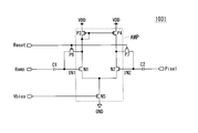
- FIG. 5 shows a specific circuit configuration of the comparison unit 1031 according to the related art.
- the comparison unit 1031 includes a differential amplifier AMP, capacitive elements C1 and C2, and transistors P6 and P7.
- the differential amplifier AMP includes transistors N1 and N2 composed of NMOSs whose sources are connected in common, and PMOSs connected between the drains of these transistors N1 and N2 and the power supply VDD, and whose gates are commonly connected. And NMOS current sources N5 connected between a node commonly connected to the sources of the transistors N1 and N2 and the ground GND.
- Transistors P6 and P7 made of PMOS are connected between the gates and drains of the transistors N1 and N2, respectively.
- the transistors P6 and P7 are turned on when a low active reset pulse Reset is given to each gate from the timing control unit 1020, and the gates and drains of the transistors N1 and N2 are short-circuited, and the transistors N1 and N2 are It functions as a reset unit that resets the voltage of the gate, that is, the voltage of the two input terminals (first input terminal IN1 and second input terminal IN2) of the differential amplifier.
- the first terminals of capacitive elements C1 and C2 for cutting the DC level are connected to the gates of the transistors N1 and N2, respectively.
- the reference signal Ramp from the reference signal generation unit 1016 is given to the second terminal of the capacitive element C1.
- a pixel signal Pixel output from each unit pixel 1003 of the imaging unit 1002 is given to the second terminal of the capacitive element C2.
- a bias voltage Vbias for controlling the current value is applied to the gate of the current source N5.
- the imaging apparatus using the lamp type AD converter according to the prior art has the following problems.
- the reference signal is shared by the large number of AD converters. For this reason, when the reference signal changes due to the influence from the comparison circuit (comparison unit 1031 in FIG. 4) according to the operation of a certain AD converter, other AD converters are affected by the influence and cause an error in the AD conversion result.
- FIG. 6 schematically shows an example of an image captured by the CMOS image sensor.
- the image shown in FIG. 6 shows an example in which a bright region (regions R0 and R2) and a dark region (region R1) are mixed.
- the signal indicating the comparison result in the comparison circuit is inverted first in the region R1 between the region R1 and the region R2.
- the reference signal is changed by feedthrough (kickback) from the comparison circuit of the region R1, and a bright region (region R2, particularly a portion adjacent to the region R1) An error occurs in the AD conversion result of the column. As a result, the image quality deteriorates.
- Method I is a method of reducing the error factor transmitted from the comparison circuit to the reference signal by the isolation capability of the buffer circuit by adding the buffer circuit to the input of each comparison circuit.
- current consumption and noise increase due to the insertion of the buffer circuit.
- Method II corresponds to reducing the resistance value of the DAC circuit.
- the current value of the current source necessary for generating the same reference signal for example, a reference voltage of 1 [V]
- the above disadvantages are the same in the reference signal generation unit using an integration circuit composed of an operational amplifier.
- the present invention provides an imaging apparatus using a lamp type AD converter that can reduce an error given to a reference signal and suppress an AD conversion error and image quality deterioration without causing an increase in current consumption and noise.
- an imaging device includes an imaging unit in which a plurality of unit pixels having photoelectric conversion elements are arranged in a matrix, and a reference signal generation that generates a reference signal that increases or decreases over time.
- Unit a first input terminal electrically connected to the reference signal generation unit, and a second input terminal electrically connected to the unit pixel, the first input terminal and the A differential amplifier that compares the voltage of the second input terminal, and a comparison unit arranged for each column or a plurality of columns of the pixel array of the imaging unit and a comparison from the comparison start to the comparison end by the comparison unit
- a measurement unit that measures time and generates data according to the comparison time
- the comparison unit includes a first capacitive element, and the first terminal of the first capacitive element is the The second terminal of the first capacitive element is electrically connected to the first input terminal. It is electrically connected to the voltage source.
- the comparison unit includes a second capacitive element, and the first terminal of the second capacitive element is the first capacitive element.
- the second terminal of the second capacitor is electrically connected to the input terminal, and the second terminal of the second capacitor is electrically connected to the first terminal of the reference signal generation unit and the first capacitor,
- the capacitance value of the capacitive element may be smaller than the capacitance value of the second capacitive element.
- the predetermined voltage source may be either a power supply or a ground.
- a first capacitive element in which the first terminal is electrically connected to the first input terminal and the second terminal is electrically connected to a predetermined voltage source.
- FIG. 1 shows an example of the configuration of the imaging apparatus according to the present embodiment.
- An imaging apparatus 1 illustrated in FIG. 1 includes an imaging unit 2, a vertical selection unit 12, a horizontal selection unit 14, a column processing unit 15, a reference signal generation unit 16, an output unit 17, and a timing control unit 20.
- the imaging unit 2 is configured by arranging a plurality of unit pixels 3 having photoelectric conversion elements in a matrix.
- the unit pixel 3 generates a pixel signal corresponding to the magnitude of the incident electromagnetic wave, and outputs the pixel signal to the vertical signal line 13 provided for each column.
- the vertical selection unit 12 selects each row of the imaging unit 2.
- the reference signal generator 16 generates a reference signal (ramp wave) that increases or decreases over time.
- the column processing unit 15 includes a column AD conversion unit 30 that performs AD conversion on the pixel signal output from the unit pixel 3.
- the horizontal selection unit 14 reads the AD-converted digital data to the horizontal signal line.
- the output unit 17 outputs the digital data read by the horizontal selection unit 14 to a subsequent circuit.
- the timing control unit 20 controls each unit.
- the imaging unit 2 configured by unit pixels 3 of 4 rows ⁇ 6 columns is described, but the number of rows and columns of the array of unit pixels 3 is an arbitrary natural number of 2 or more If it is good. Actually, tens to tens of thousands of unit pixels 3 are arranged in each row and each column of the imaging unit 2.
- the unit pixel 3 constituting the imaging unit 2 is constituted by a photoelectric conversion element such as a photodiode / photogate / phototransistor, and a transistor circuit.
- the unit pixels 3 are two-dimensionally arranged by 4 rows and 6 columns.
- a row control line 11 is wired for each row with respect to the pixel array of 4 rows and 6 columns.
- Each one end of the row control line 11 is connected to each output end corresponding to each row of the vertical selection unit 12.
- the vertical selection unit 12 includes a shift register or a decoder, and controls the row address and row scanning of the imaging unit 2 via the row control line 11 when driving each unit pixel 3 of the imaging unit 2.
- a vertical signal line 13 is wired for each column with respect to the pixel array of the imaging unit 2.
- the column processing unit 15 includes, for example, a column AD conversion unit 30 provided for each column of the pixel array of the imaging unit 2, that is, for each vertical signal line 13.
- the column AD conversion unit 30 converts an analog pixel signal read from each unit pixel 3 of the imaging unit 2 via the vertical signal line 13 for each column into digital data.
- the column AD conversion unit 30 is arranged in a one-to-one correspondence with one column of the pixel array of the imaging unit 2, but this is only an example and is limited to this arrangement relationship. is not.
- one column AD conversion unit 30 is arranged for a plurality of columns in the pixel array of the imaging unit 2, and the one column AD conversion unit 30 is used in a time-sharing manner between the plurality of columns. Is also possible.
- the column processing unit 15, together with a reference signal generation unit 16 to be described later, is an analog-digital conversion unit (AD conversion circuit) that converts an analog pixel signal read from the unit pixel 3 in the selected row of the imaging unit 2 into digital pixel data. Is configured.
- AD conversion circuit analog-digital conversion unit
- the reference signal generation unit 16 is configured by, for example, an integration circuit, generates a reference signal, a so-called ramp wave, whose level changes in an inclined manner as time elapses according to control by the timing control unit 20, and passes through the reference signal line.
- the reference signal is supplied to the column AD conversion unit 30.
- the reference signal generation unit 16 is not limited to the one using an integration circuit, and a DAC circuit may be used. However, in the case of adopting a configuration in which a ramp wave is generated digitally using a DAC circuit, it is necessary to make the step of the ramp wave fine or a configuration equivalent thereto.
- the horizontal selection unit 14 includes a shift register or a decoder, and controls the column address and column scanning of the column AD conversion unit 30 of the column processing unit 15. According to the control by the horizontal selection unit 14, the digital data AD-converted by the column AD conversion unit 30 is sequentially read out to the output unit 17 through the horizontal signal line.
- the timing control unit 20 is a TG that supplies a clock necessary for the operation of each unit such as the vertical selection unit 12, the reference signal generation unit 16, the horizontal selection unit 14, the column processing unit 15, and the output unit 17, and a pulse signal with a predetermined timing.
- Timing Generator timing generator
- Output unit 17 outputs binarized digital data.
- the output unit 17 may include a signal processing function such as black level adjustment, column variation correction, and color processing. Further, the output unit 17 may convert n-bit parallel digital data into serial data and output the serial data.
- the vertical selection unit 12, the horizontal selection unit 14, the output unit 17, and the timing control unit 20 are not characteristic configurations of the lamp type AD converter. Further, these configurations are not indispensable for obtaining the characteristic effects of the imaging apparatus 1 according to the present embodiment.
- Each of the column AD conversion units 30 compares an analog pixel signal read from each unit pixel 3 of the imaging unit 2 via the vertical signal line 13 with a reference signal for AD conversion supplied from the reference signal generation unit 16 As a result, a pulse signal having a magnitude (pulse width) in the time axis direction corresponding to the magnitude of the pixel signal is generated.
- the column AD conversion unit 30 performs AD conversion by converting the data corresponding to the pulse width period of the pulse signal into digital data corresponding to the magnitude of the pixel signal.
- the column AD conversion unit 30 is arranged for each column of the pixel array of the imaging unit 2. In FIG. 1, six column AD conversion units 30 are arranged.
- the column AD conversion unit 30 of each column is configured identically.
- the column AD conversion unit 30 includes a comparison unit 31 and a measurement unit 32. In this example, the comparison unit 31 and the measurement unit 32 are arranged for each column of the pixel array of the imaging unit 2, but the comparison unit 31 and the measurement unit 32 are arranged for each of the plurality of columns of the pixel arrangement of the imaging unit 2. It may be.
- the comparison unit 31 calculates a signal voltage corresponding to an analog pixel signal output from the unit pixel 3 of the imaging unit 2 via the vertical signal line 13, and a ramp voltage of the reference signal supplied from the reference signal generation unit 16. By comparing, the magnitude of the pixel signal is converted into information in the time axis direction (pulse width of the pulse signal).
- the comparison output of the comparison unit 31 becomes, for example, a high level (H level) when the lamp voltage is higher than the signal voltage, and becomes a low level (L level) when the lamp voltage is equal to or lower than the signal voltage.
- the comparison unit 31 ends the comparison process at a timing when the reference signal satisfies a predetermined condition with respect to the pixel signal (in this example, a timing at which the voltages of the reference signal and the pixel signal substantially match).
- the comparison output of the comparison unit 31 is inverted at the timing when the comparison unit 31 finishes the comparison process.
- the measurement unit 32 is configured by, for example, an n-bit up / down counter circuit that measures the comparison time from the comparison start to the comparison end by the comparison unit 31 and generates data corresponding to the comparison time.
- the n bits are, for example, 10 bits.
- the n bits are 10 examples, and the n bits may be less than 10 bits (for example, 8 bits), more than 10 bits (for example, 12 bits), and the like.
- the circuit constituting the measuring unit 32 need not be limited to the up / down counter circuit.
- the unit pixel 3 outputs a reset level and a signal level.
- AD conversion is performed as follows. For example, the voltage of the reference signal that falls at a predetermined inclination is compared with the voltage at the reset level or the signal level that is the pixel signal from the unit pixel 3. For example, by measuring the period from when the reference signal used in the comparison processing is generated until the signal voltage corresponding to the reset level or the signal level matches the ramp voltage of the reference signal, the reset level Alternatively, digital data corresponding to each signal level is obtained.
- the reset level including the noise of the pixel signal is read out as an analog pixel signal in the first reading operation, and then in the second reading operation.
- the signal level is read out.
- the reset level and the signal level are input to the column AD conversion unit 30 through the vertical signal line 13 in time series.
- the timing control unit 20 supplies the reference signal generation unit 16 with reference signal generation control data.
- the reference signal generator 16 outputs a reference signal whose waveform changes in a ramp shape as a whole as a comparison voltage to be applied to the first input terminal of the comparator 31.
- the comparison unit 31 compares the voltage at the first input terminal to which the reference signal from the reference signal generation unit 16 is given with the voltage at the second input terminal to which the reset level is given. When they match, the comparison output is inverted.
- the measurement unit 32 starts measurement in the down-count mode based on the comparison start in the comparison unit 31, and holds the measurement value when the comparison output of the comparison unit 31 is inverted. That is, the measuring unit 32 holds digital data corresponding to the reset level.
- the timing control unit 20 stops supplying control data to the reference signal generation unit 16 and outputting a reference clock when a predetermined period has elapsed. Thereby, the reference signal generation unit 16 stops generating the reference signal.
- the timing control unit 20 refers to the reference signal generation unit 16 Supply control data for signal generation.
- the reference signal generator 16 outputs a reference signal.
- the comparison unit 31 compares the voltage at the first input terminal to which the reference signal from the reference signal generation unit 16 is given with the voltage at the second input terminal to which the signal level is given. When they match, the comparison output is inverted.
- the timing control unit 20 stops supplying control data to the reference signal generation unit 16 and outputting a reference clock when a predetermined period has elapsed. Thereby, the reference signal generation unit 16 stops generating the reference signal.
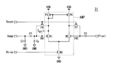
- FIG. 2 shows an example of the configuration of the comparison unit 31.
- the comparison unit 31 includes a differential amplifier AMP, transistors P6 and P7, and capacitive elements C1, C2, and C3.
- the differential amplifier AMP includes transistors N1 and N2 composed of NMOSs whose sources are connected in common, and PMOSs connected between the drains of these transistors N1 and N2 and the power supply VDD, and whose gates are commonly connected. And NMOS current sources N5 connected between a node commonly connected to the sources of the transistors N1 and N2 and the ground GND.
- the differential amplifier AMP includes a first input terminal IN1 (gate of the transistor N1) electrically connected to the reference signal generation unit 16, and a second input terminal IN2 electrically connected to the unit pixel 3. (The gate of the transistor N2) and compare the voltages of the first input terminal IN1 and the second input terminal IN2.
- Transistors P6 and P7 made of PMOS are connected between the gates and drains of the transistors N1 and N2, respectively. These transistors P6 and P7 are turned on when a low active reset pulse Reset is given to each gate from the timing controller 20, and the gates and drains of the transistors N1 and N2 are short-circuited. It functions as a reset unit that resets the voltage of the gate, that is, the voltage of the two input terminals of the differential amplifier AMP.
- the first terminals of the capacitive elements C1 and C2 for cutting the DC level are connected to the gates of the transistors N1 and N2, that is, the first input terminal IN1 and the second input terminal IN2 of the differential amplifier AMP, respectively.
- a second terminal of the capacitive element C1 (second capacitive element) is electrically connected to the reference signal generation unit 16, and is supplied with the reference signal Ramp from the reference signal generation unit 16.
- a second terminal of the capacitive element C2 is electrically connected to the unit pixel 3 of the imaging unit 2, and a pixel signal Pixel output from each unit pixel 3 is given.
- the first terminal of the capacitive element C3 (first capacitive element) is connected to the second terminal of the capacitive element C1. That is, the first terminal of the capacitive element C3 is electrically connected to the first input terminal IN1 of the differential amplifier AMP via the capacitive element C1.
- the second terminal of the capacitive element C3 is connected to the ground GND.
- a bias voltage Vbias for controlling the current value is applied to the gate of the current source N5.
- the first terminal of the capacitive element C3 is electrically connected to the first input terminal IN1 via the capacitive element C1, and the second terminal of the capacitive element C3 is connected to a predetermined voltage source (ground GND). Electrically connected.
- the first terminal of the capacitor C1 is electrically connected to the first input terminal IN1
- the second terminal of the capacitor C1 is electrically connected to the reference signal generator 16 and the first terminal of the capacitor C3. It is connected to the.
- the transistor polarity may be reversed and the power supply VDD and ground GND may be reversed. Therefore, the second terminal of the capacitive element C3 may be connected to the power supply VDD.
- the transistors P6 and P7 and the capacitive elements C1 and C2 are not essential components for obtaining the characteristic effects of the imaging device 1 according to the present embodiment.
- the timing controller 20 Before the comparison unit 31 starts comparison, the reset pulse Reset is activated (Low active). As a result, the transistors P6 and P7 are turned on to short-circuit the gates and drains of the transistors N1 and N2, and the voltages at the two input terminals are reset with the operating point of these transistors N1 and N2 as the drain voltage.
- the voltage at the two input terminals of the differential amplifier AMP that is, the offset components of the gate voltages of the transistors N1 and N2, are almost canceled at the operating point determined by this reset. That is, the voltages at the two input terminals of the differential amplifier AMP are reset so as to be substantially the same voltage. After reset, the transistors P6 and P7 are turned off.
- the voltage of the reference signal Ramp applied to the first input terminal IN1 changes in a ramp shape.
- the comparison output of the comparison unit 31 is inverted at the timing when the voltage at the first input terminal IN1 to which the reference signal Ramp is applied and the voltage at the second input terminal IN2 to which the reset level is applied substantially coincide.
- An overlap capacitance exists between the gate terminal and the drain terminal of the transistor N1 constituting the differential pair, and an input capacitance (capacitance value: C P ) is present at the gate terminal of the transistor N1.
- the capacitance value of the capacitive element C1 is C DAC
- the capacitance value of the capacitive element C3 is C LPF
- the number of column columns is n
- the current-voltage conversion resistance of the reference signal generation unit 16 is Let the resistance value be R DAC .
- the feedthrough coefficient includes the overlap capacitance (capacitance value: C gd ), the input capacitance of the gate terminal (capacitance value: C P ), and the capacitive element C3. It depends on the ratio of the capacity value to the total capacity of (capacitance value: C LPF ).
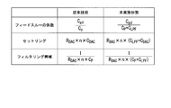
- FIG. 3 shows the feedthrough coefficient, set ring (set ring time), and filtering band in the prior art and this embodiment.
- the capacitance value C LPF of the capacitive element C3 is added to the denominator of the feedthrough coefficient in the prior art, the value of the feedthrough coefficient becomes smaller. That is, in this embodiment, the error given to the reference signal is reduced as compared with the prior art, so that AD conversion error and image quality degradation can be suppressed.
- R DAC 50 [ ⁇ ], n: 5000 [column], C DAC : 240 [fF], C LPF : 60 [fF], C P : 2 [fF] (C gs : ⁇ ⁇ 0.7C P , C gd : ⁇ ⁇ 0.3 C P )
- the value of the feedthrough coefficient can be reduced to about 1/30 compared to the prior art.
- the above C gs is an overlap capacitance between the gate terminal and the source terminal of the transistor N1.
- the filtering band of the reference signal generator 16 is reduced. As a result, there is a possibility of noise reduction.
- the capacitance value C LPF of the capacitive element C3 may be equal to or larger than the capacitive value C DAC of the capacitive element C1. That is, the imaging device 1 according to the present embodiment is not limited to the condition of the expression (1).
- the imaging unit 2 in which a plurality of unit pixels 3 having photoelectric conversion elements are arranged in a matrix, the reference signal generation unit 16 that generates a reference signal that increases or decreases over time, and the reference It has a first input terminal IN1 electrically connected to the signal generation unit 16, and a second input terminal IN2 electrically connected to the unit pixel 3, and the first input terminal IN1 and the second input terminal Comparing from the comparison unit 31 having the differential amplifier AMP for comparing the voltage of the input terminal IN2 and arranged for every one or a plurality of columns of the pixel arrangement of the imaging unit 2 from the comparison start to the comparison end by the comparison unit 31
- a measurement unit 32 that measures time and generates data according to the comparison time, and the comparison unit 31 includes a first capacitor element (capacitor element C3), and includes a first capacitor element The first terminal is electrically connected to the first input terminal IN1, and the second terminal of the first capacitor is connected to a predetermined voltage source (ground GND).
- the imaging device is configured, wherein electrically connected to
- the predetermined voltage source to which the second terminal of the capacitive element C3 is connected is the ground GND or the predetermined power source, it is not necessary to prepare a separate voltage source.
- the present invention can be widely applied to imaging devices, uses a lamp type AD converter that can reduce an error given to a reference signal, and can suppress an AD conversion error and image quality deterioration without increasing current consumption and noise.
- An imaging device is provided.
Landscapes
- Engineering & Computer Science (AREA)
- Multimedia (AREA)
- Signal Processing (AREA)
- Theoretical Computer Science (AREA)
- Transforming Light Signals Into Electric Signals (AREA)
Abstract
撮像装置は、光電変換素子を有する複数の単位画素が行列状に配置された撮像部と、参照信号を生成する参照信号生成部と、前記参照信号生成部と電気的に接続された第1の入力端子と、前記単位画素と電気的に接続された第2の入力端子とを有し、前記第1の入力端子および前記第2の入力端子の電圧を比較する差動アンプを有し、前記撮像部の画素配列の1列または複数列毎に配置された比較部と、前記比較部による比較開始から比較終了までの比較時間を計測し、前記比較時間に応じたデータを生成する計測部と、を有する。前記比較部は、第1の容量素子を有する。前記第1の容量素子の第1の端子は前記第1の入力端子に電気的に接続される。前記第1の容量素子の第2の端子は所定の電圧源に電気的に接続される。
Description
本発明は、撮像装置に関する。
本願は、2013年12月13日に、日本に出願された特願2013-258287号に基づき優先権を主張し、その内容をここに援用する。
本願は、2013年12月13日に、日本に出願された特願2013-258287号に基づき優先権を主張し、その内容をここに援用する。
従来技術に係るランプ型AD変換器を用いた撮像装置として、特許文献1あるいは特許文献2に記載された構成が知られている。初めに、従来技術に係る撮像装置の構成および動作について説明する。
図4は、従来技術に係るランプ型AD変換器を用いた撮像装置の概略構成を示している。撮像装置1001は、撮像部1002、垂直選択部1012、水平選択部1014、カラム処理部1015、参照信号生成部1016、出力部1017、タイミング制御部1020を有する。
タイミング制御部1020は、垂直選択部1012、水平選択部1014、カラム処理部1015、参照信号生成部1016、出力部1017などの各部を制御する。撮像部1002は、光電変換素子を有する複数の単位画素1003が行列状に配置されて構成されている。単位画素1003は、入射される電磁波の大きさに応じた画素信号を生成し、列毎に設けられた垂直信号線1013へ画素信号を出力する。
垂直選択部1012は、撮像部1002の各単位画素1003の駆動に際して、行制御線1011を介して撮像部1002の行アドレスや行走査の制御を行う。水平選択部1014は、カラム処理部1015の列AD変換部1030の列アドレスや列走査の制御を行う。
カラム処理部1015は、撮像部1002の列毎に設けられた列AD変換部1030を有する。列AD変換部1030は、撮像部1002の各単位画素1003から列毎に出力される画素信号であるアナログ信号をデジタルデータに変換して出力する。参照信号生成部1016は、例えば積分回路やDAC回路で構成され、時間の経過とともにレベルが傾斜状に変化する参照信号を生成する。
次に、列AD変換部1030の構成について説明する。列AD変換部1030は全て略同一に構成され、各々の列AD変換部1030は、比較部1031および計測部1032を有する。
比較部1031は、一般的に良く知られている差動アンプを基本構成とするコンパレータ回路である。比較部1031は、撮像部1002の単位画素1003から出力される画素信号と参照信号とを比較し、例えば参照信号が画素信号よりも大なるときはHighレベル、例えば参照信号が画素信号よりも小なるときはLowレベルを出力する。
計測部1032は、アップ/ダウンカウンタ回路で構成され、比較部1031が比較を開始してから比較を終了するまでの比較時間を計測し、比較時間に応じたデータを生成する。これにより、画素信号の大きさに応じたデータが得られる。水平選択部1014は、シフトレジスタやデコーダなどによって構成され、カラム処理部1015における各列AD変換部1030の列アドレスや列走査の制御を行う。これにより、AD変換されたデジタルデータは順に水平信号線を経由して出力部1017に出力される。
次に、AD変換動作について説明する。単位画素1003の具体的な動作については説明を省略するが、単位画素1003からは画素信号としてリセットレベルと信号レベルとが出力される。
まず、単位画素1003から読み出されたリセットレベルが安定した後、比較部1031を構成する差動アンプの2つの入力端子の電圧のリセットが行われる。その後、比較部1031は、参照信号とリセットレベルとの比較を行い、参照信号がリセットレベルに対して所定の条件を満たしたタイミングで比較処理を終了する。計測部1032はダウンカウントモードで比較時間の計測を実施する。比較処理の終了時点の計測値がリセットレベルのデジタルデータとなる。
続いて、単位画素1003からの信号レベルの読出し時には、比較部1031におけるリセット動作は行わない。単位画素1003から読み出された信号レベルが安定した後、比較部1031は、参照信号と信号レベルとの比較を行い、参照信号が信号レベルに対して所定の条件を満たしたタイミングで比較処理を終了する。計測部1032はアップカウントモードで比較時間の計測を実施する。比較処理の終了時点の計測値が信号成分(信号レベルからリセットレベルを減算した信号)のデジタルデータとなる。
図5は、従来技術に係る比較部1031の具体的な回路構成を示している。比較部1031は、差動アンプAMP、容量素子C1,C2、トランジスタP6,P7を有する。
差動アンプAMPは、ソースが共通に接続されたNMOSで構成されるトランジスタN1,N2と、これらトランジスタN1,N2の各ドレインと電源VDDとの間に接続され、ゲートが共通に接続されたPMOSで構成されるトランジスタP3,P4と、トランジスタN1,N2のソースに共通に接続されたノードとグランドGNDとの間に接続されたNMOSの電流源N5とを有する。
トランジスタN1,N2の各ゲートとドレインとの間に、PMOSで構成されるトランジスタP6,P7がそれぞれ接続されている。これらトランジスタP6,P7は、各ゲートにLowアクティブのリセットパルスResetがタイミング制御部1020から与えられることでON状態となり、トランジスタN1,N2の各ゲートとドレインとを短絡し、トランジスタN1,N2の各ゲートの電圧、即ち差動アンプの2つの入力端子(第1の入力端子IN1および第2の入力端子IN2)の電圧をリセットするリセット部として機能する。
トランジスタN1,N2の各ゲートには、DCレベルをカットするための容量素子C1,C2の第1の端子がそれぞれ接続されている。容量素子C1の第2の端子には、参照信号生成部1016からの参照信号Rampが与えられる。容量素子C2の第2の端子には、撮像部1002の各単位画素1003から出力される画素信号Pixelが与えられる。また、電流源N5のゲートには、電流値を制御するためのバイアス電圧Vbiasが与えられる。
しかしながら、従来技術に係るランプ型AD変換器を用いた撮像装置には、以下の課題がある。
CMOSイメージセンサのカラムパラレルなランプ型AD変換器に代表されるように、多数のランプ型AD変換器を構成する場合には、参照信号はこれらの多数のAD変換器で共通化される。そのため、あるAD変換器の動作に応じて比較回路(図4の比較部1031)からの影響により参照信号が変化すると、他のAD変換器がその影響を受けてAD変換結果に誤差を生じる。
図6は、CMOSイメージセンサが撮像する画像の例を模式的に示している。図6に示す画像は、明るい領域(領域R0,R2)と暗い領域(領域R1)とが混在する例を示している。この例では、比較回路における比較結果を示す信号は、領域R1と領域R2とでは、領域R1のほうが先に反転する。領域R1の比較結果を示す信号が先に反転すると、領域R1の比較回路からのフィードスルー(キックバック)により、参照信号が変化させられ、明るい領域(領域R2、特に領域R1に隣接する部分)のカラムのAD変換結果に誤差を生じる。その結果、画質が劣化する。
この影響を改善する方法として、以下の方法が考えられる。
I) ソースフォロワ回路に代表されるようなバッファ回路を各比較回路の入力に加える方法
II) 参照信号生成部(そのDAC回路)の出力インピーダンスを低減する方法
I) ソースフォロワ回路に代表されるようなバッファ回路を各比較回路の入力に加える方法
II) 参照信号生成部(そのDAC回路)の出力インピーダンスを低減する方法
I)の方法は、バッファ回路を各比較回路の入力に加えることで、比較回路から参照信号へと伝達される誤差要因をバッファ回路のアイソレーション能力によって低減する方法である。しかし、この方法ではバッファ回路の挿入によって、消費電流・雑音が増大する。
II)の方法は、DAC回路の抵抗値を低減することに相当する。この結果、同一の参照信号(例えば1[V]の参照電圧)を生成するために必要な電流源の電流値が増大する。したがって、消費電流が増大する。演算増幅器から構成される積分回路を用いた参照信号生成部においても上記の不利益は同様である。
本発明は、参照信号に与える誤差を低減でき、消費電流、雑音の増大を招くことなくAD変換誤差や画質劣化を抑圧することができるランプ型AD変換器を用いた撮像装置を提供する。
本発明の第1態様によれば、撮像装置は、光電変換素子を有する複数の単位画素が行列状に配置された撮像部と、時間の経過とともに増加あるいは減少する参照信号を生成する参照信号生成部と、前記参照信号生成部と電気的に接続された第1の入力端子と、前記単位画素と電気的に接続された第2の入力端子とを有し、前記第1の入力端子および前記第2の入力端子の電圧を比較する差動アンプを有し、前記撮像部の画素配列の1列または複数列毎に配置された比較部と、前記比較部による比較開始から比較終了までの比較時間を計測し、前記比較時間に応じたデータを生成する計測部と、を有し、前記比較部は、第1の容量素子を有し、前記第1の容量素子の第1の端子は前記第1の入力端子に電気的に接続され、前記第1の容量素子の第2の端子は所定の電圧源に電気的に接続される。
また、本発明の第2態様によれば、第1態様の撮像装置において、前記比較部は、第2の容量素子を有し、前記第2の容量素子の第1の端子は前記第1の入力端子に電気的に接続され、前記第2の容量素子の第2の端子は前記参照信号生成部および前記第1の容量素子の前記第1の端子に電気的に接続され、前記第1の容量素子の容量値は、前記第2の容量素子の容量値よりも小さな値であってもよい。
また、本発明の第3態様によれば、第1態様または第2態様の撮像装置において、前記所定の電圧源は、電源およびグランドのいずれかであってもよい。
本発明の各態様によれば、第1の端子が第1の入力端子に電気的に接続され、第2の端子が所定の電圧源に電気的に接続された第1の容量素子を設けることによって、参照信号に与える誤差を低減でき、消費電流、雑音の増大を招くことなくAD変換誤差や画質劣化を抑圧することができる。
以下、図面を参照し、本発明の実施形態を説明する。図1は、本実施形態に係る撮像装置の構成の一例を示している。図1に示す撮像装置1は、撮像部2、垂直選択部12、水平選択部14、カラム処理部15、参照信号生成部16、出力部17、タイミング制御部20を有する。
撮像部2は、光電変換素子を有する複数の単位画素3が行列状に配置されて構成されている。単位画素3は、入射される電磁波の大きさに応じた画素信号を生成し、列毎に設けられた垂直信号線13へ画素信号を出力する。垂直選択部12は、撮像部2の各行を選択する。参照信号生成部16は、時間の経過とともに増加または減少する参照信号(ランプ波)を生成する。カラム処理部15は、単位画素3から出力された画素信号をAD変換する列AD変換部30を有する。水平選択部14は、AD変換されたデジタルデータを水平信号線に読み出す。出力部17は、水平選択部14によって読み出されたデジタルデータを後段の回路に出力する。タイミング制御部20は各部を制御する。
図1では、簡単のため4行×6列の単位画素3から構成される撮像部2の場合について説明しているが、単位画素3の配列の行数および列数は2以上の任意の自然数であれば良い。現実には、撮像部2の各行や各列には、数十から数万の単位画素3が配置される。図示を割愛するが、撮像部2を構成する単位画素3は、フォトダイオード/フォトゲート/フォトトランジスタなどの光電変換素子、およびトランジスタ回路によって構成されている。
以下では、各部のより詳細な説明を行う。撮像部2では、単位画素3が4行6列分だけ2次元に配置されている。また、この4行6列の画素配列に対して行毎に行制御線11が配線されている。行制御線11の各一端は、垂直選択部12の各行に対応した各出力端に接続されている。垂直選択部12は、シフトレジスタあるいはデコーダなどによって構成され、撮像部2の各単位画素3の駆動に際して、行制御線11を介して撮像部2の行アドレスや行走査の制御を行う。また、撮像部2の画素配列に対して列毎に垂直信号線13が配線されている。
カラム処理部15は、例えば撮像部2の画素配列の列毎、即ち垂直信号線13毎に設けられた列AD変換部30を有する。列AD変換部30は、撮像部2の各単位画素3から列毎に垂直信号線13を介して読み出されるアナログの画素信号をデジタルデータに変換する。本例では、撮像部2の画素配列の1列に対して1対1の対応関係で列AD変換部30が配置されているが、これは一例に過ぎず、この配置関係に限定されるものではない。例えば、撮像部2の画素配列の複数の列に対して列AD変換部30を1つ配置し、この1つの列AD変換部30を複数の列間で時分割にて使用する構成をとることも可能である。カラム処理部15は、後述する参照信号生成部16と共に、撮像部2の選択行の単位画素3から読み出されるアナログの画素信号をデジタルの画素データに変換するアナログ-デジタル変換手段(AD変換回路)を構成している。
参照信号生成部16は、例えば積分回路によって構成され、タイミング制御部20による制御に従って、時間が経過するにつれてレベルが傾斜状に変化する、参照信号、いわゆるランプ波を生成し、参照信号線を介して列AD変換部30に参照信号を供給する。参照信号生成部16としては、積分回路を用いたものに限られるものではなく、DAC回路を用いても構わない。ただし、DAC回路を用いてデジタル的にランプ波を生成する構成をとる場合には、ランプ波のステップを細かくする、あるいはそれと同等な構成をとる必要がある。
水平選択部14は、シフトレジスタあるいはデコーダなどによって構成され、カラム処理部15の列AD変換部30の列アドレスや列走査の制御を行う。この水平選択部14による制御に従って、列AD変換部30でAD変換されたデジタルデータは順に水平信号線を介して出力部17に読み出される。
タイミング制御部20は、垂直選択部12、参照信号生成部16、水平選択部14、カラム処理部15、出力部17などの各部の動作に必要なクロックや所定タイミングのパルス信号を供給するTG(=Timing Generator:タイミングジェネレータ)の機能ブロックと、このTGと通信を行うための機能ブロックとを備える。
出力部17は、2進化したデジタルデータを出力する。また、出力部17は、バッファリング機能以外に、例えば黒レベル調整、列バラツキ補正、色処理などの信号処理機能を内蔵しても構わない。更に、出力部17がnビットパラレルのデジタルデータをシリアルデータに変換して出力するようにしても構わない。
撮像装置1における構成のうち、垂直選択部12、水平選択部14、出力部17、タイミング制御部20は、ランプ型AD変換器の特徴的な構成ではない。また、これらの構成は、本実施形態に係る撮像装置1の特徴的な効果を得るために必須の構成ではない。
次に、列AD変換部30の構成について説明する。列AD変換部30は各々、撮像部2の各単位画素3から垂直信号線13を介して読み出されるアナログの画素信号を、参照信号生成部16から与えられる、AD変換するための参照信号と比較することにより、画素信号の大きさに対応した時間軸方向の大きさ(パルス幅)を持つパルス信号を生成する。そして、列AD変換部30は、このパルス信号のパルス幅の期間に対応したデータを画素信号の大きさに応じたデジタルデータとすることによってAD変換を行う。
以下では、列AD変換部30の構成の詳細について説明する。列AD変換部30は撮像部2の画素配列の列毎に配置されている。図1では6個の列AD変換部30が配置されている。各列の列AD変換部30は同一に構成されている。列AD変換部30は、比較部31および計測部32を有する。本例では、比較部31および計測部32は撮像部2の画素配列の1列毎に配置されているが、比較部31および計測部32が撮像部2の画素配列の複数列毎に配置されていてもよい。
比較部31は、撮像部2の単位画素3から垂直信号線13を介して出力されるアナログの画素信号に応じた信号電圧と、参照信号生成部16から供給される参照信号のランプ電圧とを比較することによって、画素信号の大きさを、時間軸方向の情報(パルス信号のパルス幅)に変換する。比較部31の比較出力は、例えばランプ電圧が信号電圧よりも大なるときにはHighレベル(Hレベル)になり、ランプ電圧が信号電圧以下のときにはLowレベル(Lレベル)になる。比較部31は、参照信号が画素信号に対して所定の条件を満たしたタイミング(本例では参照信号と画素信号との電圧が略一致したタイミング)で比較処理を終了する。比較部31が比較処理を終了するタイミングで比較部31の比較出力が反転する。
計測部32は、比較部31による比較開始から比較終了までの比較時間を計測し、比較時間に応じたデータを生成する、例えばnビットのアップ/ダウンカウンタ回路で構成される。nビットは例えば10ビットである。nビットが10ビットであるのは一例であって、nビットが10ビット未満のビット数(例えば、8ビット)や10ビットを超えるビット数(例えば、12ビット)などであっても構わない。また、計測部32を構成する回路はアップ/ダウンカウンタ回路に限る必要もない。
次に、本例の動作について説明する。ここでは、単位画素3の具体的な動作については説明を省略するが、周知のように単位画素3からはリセットレベルと信号レベルとが出力される。
AD変換は、以下のようにして行われる。例えば所定の傾きで下降する参照信号の電圧と、単位画素3からの画素信号であるリセットレベルあるいは信号レベルの電圧とが比較される。この比較処理で用いる参照信号が生成された時点から、リセットレベルや信号レベルに応じた信号電圧と参照信号のランプ電圧とが一致するまでの期間を、例えば基準クロックで計測することによって、リセットレベルあるいは信号レベルの各大きさに対応したデジタルデータが得られる。
ここで、撮像部2の選択行の各単位画素3からは、アナログの画素信号として、1回目の読出し動作で画素信号の雑音を含むリセットレベルが読み出され、その後、2回目の読出し動作で信号レベルが読み出される。そして、リセットレベルと信号レベルとが垂直信号線13を通して列AD変換部30に時系列で入力される。
<1回目の読出し>
撮像部2の画素配列の任意の行の単位画素3から垂直信号線13へ出力された画素信号(リセットレベル)が安定した後、比較部31のリセット動作が行われる。その後、タイミング制御部20は、参照信号生成部16に対して、参照信号生成の制御データを供給する。これを受けて参照信号生成部16は、比較部31の第1の入力端子に与える比較電圧として、波形が全体として時間的にランプ状に変化する参照信号を出力する。比較部31は、参照信号生成部16からの参照信号が与えられた第1の入力端子の電圧と、リセットレベルが与えられた第2の入力端子の電圧とを比較し、双方の電圧が略一致したときに、比較出力を反転させる。
撮像部2の画素配列の任意の行の単位画素3から垂直信号線13へ出力された画素信号(リセットレベル)が安定した後、比較部31のリセット動作が行われる。その後、タイミング制御部20は、参照信号生成部16に対して、参照信号生成の制御データを供給する。これを受けて参照信号生成部16は、比較部31の第1の入力端子に与える比較電圧として、波形が全体として時間的にランプ状に変化する参照信号を出力する。比較部31は、参照信号生成部16からの参照信号が与えられた第1の入力端子の電圧と、リセットレベルが与えられた第2の入力端子の電圧とを比較し、双方の電圧が略一致したときに、比較出力を反転させる。
計測部32は、比較部31での比較開始に基づいてダウンカウントモードで計測を開始し、比較部31の比較出力が反転した時点の計測値を保持する。つまり、計測部32は、リセットレベルに応じたデジタルデータを保持する。タイミング制御部20は、所定の期間を経過すると、参照信号生成部16への制御データの供給と、基準クロックの出力とを停止する。これにより、参照信号生成部16は、参照信号の生成を停止する。
<2回目の読出し>
続いて、2回目の読出し時には、単位画素3毎の入射光量に応じた信号レベルが読み出される。この2回目の読出し時には、比較部31のリセット動作は行わない。
続いて、2回目の読出し時には、単位画素3毎の入射光量に応じた信号レベルが読み出される。この2回目の読出し時には、比較部31のリセット動作は行わない。
撮像部2の画素配列の任意の行の単位画素3から垂直信号線13へ出力された画素信号(信号レベル)が安定した後、タイミング制御部20は、参照信号生成部16に対して、参照信号生成の制御データを供給する。これを受けて参照信号生成部16は参照信号を出力する。比較部31は、参照信号生成部16からの参照信号が与えられた第1の入力端子の電圧と、信号レベルが与えられた第2の入力端子の電圧とを比較し、双方の電圧が略一致したときに、比較出力を反転させる。
計測部32は、比較部31での比較開始に基づいてアップカウントモードで計測を開始し、比較部31の比較出力が反転した時点の計測値を保持する。つまり、計測部32は、信号レベルからリセットレベルを減算(CDS(=Correlated Double Sampling:相関2重サンプリング)処理)した信号成分に応じたデジタルデータを保持する。タイミング制御部20は、所定の期間を経過すると、参照信号生成部16への制御データの供給と、基準クロックの出力とを停止する。これにより、参照信号生成部16は、参照信号の生成を停止する。
次に、比較部31の詳細な構成について説明する。図2は比較部31の構成の一例を示している。比較部31は、差動アンプAMP、トランジスタP6,P7、容量素子C1,C2,C3を有する。
差動アンプAMPは、ソースが共通に接続されたNMOSで構成されるトランジスタN1,N2と、これらトランジスタN1,N2の各ドレインと電源VDDとの間に接続され、ゲートが共通に接続されたPMOSで構成されるトランジスタP3,P4と、トランジスタN1,N2のソースに共通に接続されたノードとグランドGNDとの間に接続されたNMOSの電流源N5とを有する。また、差動アンプAMPは、参照信号生成部16と電気的に接続された第1の入力端子IN1(トランジスタN1のゲート)と、単位画素3と電気的に接続された第2の入力端子IN2(トランジスタN2のゲート)とを有し、第1の入力端子IN1および第2の入力端子IN2の電圧を比較する。
トランジスタN1,N2の各ゲートとドレインとの間に、PMOSで構成されるトランジスタP6,P7がそれぞれ接続されている。これらトランジスタP6,P7は、各ゲートにLowアクティブのリセットパルスResetがタイミング制御部20から与えられることでON状態となり、トランジスタN1,N2の各ゲートとドレインとを短絡し、トランジスタN1,N2の各ゲートの電圧、即ち差動アンプAMPの2つの入力端子の電圧をリセットするリセット部として機能する。
トランジスタN1,N2の各ゲート、即ち差動アンプAMPの第1の入力端子IN1および第2の入力端子IN2には、DCレベルをカットするための容量素子C1,C2の第1の端子がそれぞれ接続されている。容量素子C1(第2の容量素子)の第2の端子は、参照信号生成部16に電気的に接続され、参照信号生成部16からの参照信号Rampが与えられる。容量素子C2の第2の端子は、撮像部2の単位画素3に電気的に接続され、各単位画素3から出力される画素信号Pixelが与えられる。
容量素子C3(第1の容量素子)の第1の端子は容量素子C1の第2の端子に接続されている。即ち、容量素子C3の第1の端子は、容量素子C1を介して差動アンプAMPの第1の入力端子IN1に電気的に接続されている。容量素子C3の第2の端子はグランドGNDに接続されている。また、電流源N5のゲートには、電流値を制御するためのバイアス電圧Vbiasが与えられる。
言い換えると、容量素子C3の第1の端子は、容量素子C1を介して第1の入力端子IN1に電気的に接続され、容量素子C3の第2の端子は所定の電圧源(グランドGND)に電気的に接続されている。また、容量素子C1の第1の端子は第1の入力端子IN1に電気的に接続され、容量素子C1の第2の端子は参照信号生成部16および容量素子C3の第1の端子に電気的に接続されている。
図2において、トランジスタの極性を逆にし、電源VDDとグランドGNDとを逆にしてもよい。したがって、容量素子C3の第2の端子は電源VDDに接続されていてもよい。
比較部31における構成のうち、トランジスタP6,P7、容量素子C1,C2は、本実施形態に係る撮像装置1の特徴的な効果を得るために必須の構成ではない。
次に、比較部31の動作について説明する。単位画素3からの画素信号Pixelとしてリセットレベルが第2の入力端子IN2に与えられ、参照信号生成部16から第1の入力端子IN1に与えられる参照信号Rampが安定した後、タイミング制御部20が比較部31の比較開始前にリセットパルスResetを活性化(Lowアクティブ)する。これにより、トランジスタP6,P7がON状態となってトランジスタN1,N2の各ゲートとドレインとを短絡し、これらトランジスタN1,N2の動作点をドレイン電圧として2つの入力端子の電圧がリセットされる。
このリセットによって決定された動作点で、差動アンプAMPの2つの入力端子の電圧、即ちトランジスタN1,N2の各ゲート電圧のオフセット成分がほぼキャンセルされる。即ち、差動アンプAMPの2つの入力端子の電圧が、略同一の電圧になるようにリセットされる。リセット後、トランジスタP6,P7はOFF状態となる。
続いて、第1の入力端子IN1に与えられる参照信号Rampの電圧がランプ状に変化する。参照信号Rampが与えられた第1の入力端子IN1の電圧と、リセットレベルが与えられた第2の入力端子IN2の電圧とが略一致したタイミングで比較部31の比較出力が反転する。
単位画素3からの画素信号Pixelとして信号レベルが第2の入力端子IN2に与えられたときの動作は、トランジスタP6,P7によるリセットが行われない点を除いて上記の動作と同様であるので、説明を省略する。
<従来技術と本実施形態におけるフィードスルーおよびその比較>
以下では、比較部31の比較出力が反転したときのフィードスルー、つまり比較部31から参照信号へと伝達される誤差要因について述べる。
以下では、比較部31の比較出力が反転したときのフィードスルー、つまり比較部31から参照信号へと伝達される誤差要因について述べる。
差動対を構成するトランジスタN1のゲート端子とドレイン端子との間にはオーバーラップ容量(容量値:Cgd)が存在し、トランジスタN1のゲート端子には入力容量(容量値:CP)、が存在する。また、容量素子C1の容量値をCDAC、容量素子C3の容量値をCLPF、カラム列数(列AD変換部30の数)をn、参照信号生成部16を構成する電流電圧変換抵抗の抵抗値をRDAC、とする。ここで、容量素子C1(容量値:CDAC)、容量素子C3(容量値:CLPF)、ゲート端子の入力容量(容量値:CP)、との間に、以下の(1)式の関係を成立させることが可能である。
CDAC > CLPF> CP ・・・(1)
CDAC > CLPF> CP ・・・(1)
比較部31の比較出力が反転すると、反転に係るトランジスタN1のドレイン電圧の変化が、オーバーラップ容量(容量値:Cgd)を介して参照信号Ramp側に伝達される(フィードスルー)。容量素子C3を設けない従来技術におけるフィードスルーの係数は、オーバーラップ容量(容量値:Cgd)と、ゲート端子の入力容量(容量値:CP)との容量値の比に依存する。これに対して、容量素子C3を設けた本実施形態における、フィードスルーの係数は、オーバーラップ容量(容量値:Cgd)と、ゲート端子の入力容量(容量値:CP)および容量素子C3(容量値:CLPF)の合計容量との容量値の比に依存する。
図3は、従来技術と本実施形態とにおけるフィードスルーの係数、セットリング(セットリング時間)、フィルタリング帯域を示している。本実施形態では、従来技術におけるフィードスルーの係数の分母に対して容量素子C3の容量値CLPFが加わるため、フィードスルーの係数の値がより小さくなる。つまり、本実施形態では、従来技術と比較して、参照信号に与える誤差が低減されるので、AD変換誤差や画質劣化を抑圧することができる。例えば、RDAC:50[Ω]、n:5000[列]、CDAC:240[fF]、CLPF:60[fF]、CP:2[fF](Cgs:~×0.7CP 、Cgd:~×0.3 CP )である場合、本実施形態では、従来技術に比較してフィードスルーの係数の値を1/30程度に低減することが可能である。上記のCgsはトランジスタN1のゲート端子とソース端子との間のオーバーラップ容量である。
容量素子C3を設けることで、比較部31のリセット(バランス)時のセットリングが長くなることが懸念される。しかし、容量素子C3の容量値CLPFが(1)式の条件を満たすように容量素子C3を構成することで、上記の効果を維持しつつ、セットリングの増大を抑圧することができる。
容量素子C3を設けることに付随する効果として、参照信号生成部16のフィルタリング帯域が低減する。結果的に、ノイズ低減の可能性がある。
セットリングへの影響を無視できる場合、容量素子C3の容量値CLPFは容量素子C1の容量値CDAC以上であってもよい。つまり、本実施形態に係る撮像装置1は、(1)式の条件に限定されない。
本実施形態によれば、光電変換素子を有する複数の単位画素3が行列状に配置された撮像部2と、時間の経過とともに増加あるいは減少する参照信号を生成する参照信号生成部16と、参照信号生成部16と電気的に接続された第1の入力端子IN1と、単位画素3と電気的に接続された第2の入力端子IN2とを有し、第1の入力端子IN1および第2の入力端子IN2の電圧を比較する差動アンプAMPを有し、撮像部2の画素配列の1列または複数列毎に配置された比較部31と、比較部31による比較開始から比較終了までの比較時間を計測し、比較時間に応じたデータを生成する計測部32と、を有し、比較部31は、第1の容量素子(容量素子C3)を有し、第1の容量素子の第1の端子は第1の入力端子IN1に電気的に接続され、第1の容量素子の第2の端子は所定の電圧源(グランドGNDまたは所定の電源)に電気的に接続される、ことを特徴とする撮像装置が構成される。
本実施形態では、前述したI)およびII)の方法を用いることなく、フィードスルーを低減することが可能となる。したがって、参照信号に与える誤差を低減でき、消費電流、雑音の増大を招くことなくAD変換誤差や画質劣化を抑圧することができる。
また、(1)式のように、容量素子C3の容量値を容量素子C1の容量値よりも小さな値にすることによって、上記の効果を維持したまま、リセット時のセットリング時間の増大を抑圧することができる。
また、容量素子C3の第2の端子が接続される所定の電圧源をグランドGNDまたは所定の電源とすることによって、別途電圧源を用意する必要がなくなる。
以上、図面を参照して本発明の実施形態について詳述してきたが、具体的な構成は上記の実施形態に限られるものではなく、本発明の要旨を逸脱しない範囲の設計変更等も含まれる。
本発明は、撮像装置に広く適用でき、参照信号に与える誤差を低減でき、消費電流、雑音の増大を招くことなくAD変換誤差や画質劣化を抑圧することができるランプ型AD変換器を用いた撮像装置を提供する。
1,1001 撮像装置
2,1002 撮像部
3,1003 単位画素
11,1011 行制御線
12,1012 垂直選択部
13,1013 垂直信号線
14,1014 水平選択部
15,1015 カラム処理部
16,1016 参照信号生成部
17,1017 出力部
20,1020 タイミング制御部
30,1030 列AD変換部
31,1031 比較部
32,1032 計測部
2,1002 撮像部
3,1003 単位画素
11,1011 行制御線
12,1012 垂直選択部
13,1013 垂直信号線
14,1014 水平選択部
15,1015 カラム処理部
16,1016 参照信号生成部
17,1017 出力部
20,1020 タイミング制御部
30,1030 列AD変換部
31,1031 比較部
32,1032 計測部
Claims (3)
- 光電変換素子を有する複数の単位画素が行列状に配置された撮像部と、
時間の経過とともに増加あるいは減少する参照信号を生成する参照信号生成部と、
前記参照信号生成部と電気的に接続された第1の入力端子と、前記単位画素と電気的に接続された第2の入力端子とを有し、前記第1の入力端子および前記第2の入力端子の電圧を比較する差動アンプを有し、前記撮像部の画素配列の1列または複数列毎に配置された比較部と、
前記比較部による比較開始から比較終了までの比較時間を計測し、前記比較時間に応じたデータを生成する計測部と、
を有し、
前記比較部は、第1の容量素子を有し、
前記第1の容量素子の第1の端子は前記第1の入力端子に電気的に接続され、前記第1の容量素子の第2の端子は所定の電圧源に電気的に接続される、
撮像装置。 - 前記比較部は、第2の容量素子を有し、
前記第2の容量素子の第1の端子は前記第1の入力端子に電気的に接続され、前記第2の容量素子の第2の端子は前記参照信号生成部および前記第1の容量素子の前記第1の端子に電気的に接続され、
前記第1の容量素子の容量値は、前記第2の容量素子の容量値よりも小さな値である、
請求項1に係る撮像装置。 - 前記所定の電圧源は、電源およびグランドのいずれかである、
請求項1および請求項2の何れか一項に係る撮像装置。
Priority Applications (1)
| Application Number | Priority Date | Filing Date | Title |
|---|---|---|---|
| US14/817,821 US9462204B2 (en) | 2013-12-13 | 2015-08-04 | Analog to digital converter for imaging device |
Applications Claiming Priority (2)
| Application Number | Priority Date | Filing Date | Title |
|---|---|---|---|
| JP2013-258287 | 2013-12-13 | ||
| JP2013258287A JP5771673B2 (ja) | 2013-12-13 | 2013-12-13 | 撮像装置 |
Related Child Applications (1)
| Application Number | Title | Priority Date | Filing Date |
|---|---|---|---|
| US14/817,821 Continuation US9462204B2 (en) | 2013-12-13 | 2015-08-04 | Analog to digital converter for imaging device |
Publications (1)
| Publication Number | Publication Date |
|---|---|
| WO2015087608A1 true WO2015087608A1 (ja) | 2015-06-18 |
Family
ID=53370927
Family Applications (1)
| Application Number | Title | Priority Date | Filing Date |
|---|---|---|---|
| PCT/JP2014/076992 Ceased WO2015087608A1 (ja) | 2013-12-13 | 2014-10-08 | 撮像装置 |
Country Status (3)
| Country | Link |
|---|---|
| US (1) | US9462204B2 (ja) |
| JP (1) | JP5771673B2 (ja) |
| WO (1) | WO2015087608A1 (ja) |
Citations (2)
| Publication number | Priority date | Publication date | Assignee | Title |
|---|---|---|---|---|
| JP2013172270A (ja) * | 2012-02-20 | 2013-09-02 | Sony Corp | 比較器、ad変換器、固体撮像装置、カメラシステム、および電子機器 |
| JP2013187744A (ja) * | 2012-03-08 | 2013-09-19 | Olympus Corp | 撮像装置 |
Family Cites Families (5)
| Publication number | Priority date | Publication date | Assignee | Title |
|---|---|---|---|---|
| JP2006020171A (ja) * | 2004-07-02 | 2006-01-19 | Fujitsu Ltd | 差動型コンパレータ、アナログ・デジタル変換装置、撮像装置 |
| JP4442515B2 (ja) | 2005-06-02 | 2010-03-31 | ソニー株式会社 | 固体撮像装置、固体撮像装置におけるアナログ−デジタル変換方法および撮像装置 |
| JP5407264B2 (ja) | 2008-10-09 | 2014-02-05 | ソニー株式会社 | 固体撮像素子およびカメラシステム |
| JP5178458B2 (ja) * | 2008-10-31 | 2013-04-10 | キヤノン株式会社 | 固体撮像装置、撮像システム、および、固体撮像装置の駆動方法 |
| WO2012143982A1 (ja) * | 2011-04-21 | 2012-10-26 | パナソニック株式会社 | ランプ生成回路、並びにそれを備えたイメージセンサーおよび撮像装置 |
-
2013
- 2013-12-13 JP JP2013258287A patent/JP5771673B2/ja active Active
-
2014
- 2014-10-08 WO PCT/JP2014/076992 patent/WO2015087608A1/ja not_active Ceased
-
2015
- 2015-08-04 US US14/817,821 patent/US9462204B2/en active Active
Patent Citations (2)
| Publication number | Priority date | Publication date | Assignee | Title |
|---|---|---|---|---|
| JP2013172270A (ja) * | 2012-02-20 | 2013-09-02 | Sony Corp | 比較器、ad変換器、固体撮像装置、カメラシステム、および電子機器 |
| JP2013187744A (ja) * | 2012-03-08 | 2013-09-19 | Olympus Corp | 撮像装置 |
Also Published As
| Publication number | Publication date |
|---|---|
| JP5771673B2 (ja) | 2015-09-02 |
| US20150341583A1 (en) | 2015-11-26 |
| JP2015115872A (ja) | 2015-06-22 |
| US9462204B2 (en) | 2016-10-04 |
Similar Documents
| Publication | Publication Date | Title |
|---|---|---|
| JP5067011B2 (ja) | 固体撮像装置、撮像装置、電子機器 | |
| JP5704939B2 (ja) | 撮像装置 | |
| JP4725608B2 (ja) | 比較器、比較器の校正方法、固体撮像素子、およびカメラシステム | |
| KR101241485B1 (ko) | 고체 촬상 장치, 고체 촬상 장치에서의 아날로그-디지털변환 방법 및 촬상 장치 | |
| JP7562262B2 (ja) | 比較装置及びそれを含むイメージセンサ | |
| JP6164797B2 (ja) | 信号受信部テスト回路、撮像装置、信号受信部テスト方法、撮像装置のテスト方法 | |
| JP6249881B2 (ja) | 固体撮像装置および撮像装置 | |
| WO2017179319A1 (ja) | 固体撮像素子、電子機器、および、固体撮像素子の制御方法 | |
| JP5941816B2 (ja) | Ad変換回路および固体撮像装置 | |
| KR20090014103A (ko) | 참조 전압 회로 및 촬상 회로 | |
| JP5953074B2 (ja) | 撮像装置 | |
| JP5941783B2 (ja) | 撮像装置 | |
| CN111193881A (zh) | 低条带噪声的比较器及包括其的cmos图像传感器 | |
| CN115514904A (zh) | 固态图像感测设备 | |
| US11363225B2 (en) | Image sensor | |
| US10757356B2 (en) | Comparison device and CMOS image sensor including the same | |
| JP5771673B2 (ja) | 撮像装置 | |
| JP5070945B2 (ja) | 固体撮像装置、撮像装置 | |
| WO2018173196A1 (ja) | シングルエンド型ad変換器、ad変換回路、およびイメージセンサ |
Legal Events
| Date | Code | Title | Description |
|---|---|---|---|
| 121 | Ep: the epo has been informed by wipo that ep was designated in this application |
Ref document number: 14869182 Country of ref document: EP Kind code of ref document: A1 |
|
| NENP | Non-entry into the national phase |
Ref country code: DE |
|
| 122 | Ep: pct application non-entry in european phase |
Ref document number: 14869182 Country of ref document: EP Kind code of ref document: A1 |