WO2015083456A1 - 高周波用電線およびコイル - Google Patents
高周波用電線およびコイル Download PDFInfo
- Publication number
- WO2015083456A1 WO2015083456A1 PCT/JP2014/078345 JP2014078345W WO2015083456A1 WO 2015083456 A1 WO2015083456 A1 WO 2015083456A1 JP 2014078345 W JP2014078345 W JP 2014078345W WO 2015083456 A1 WO2015083456 A1 WO 2015083456A1
- Authority
- WO
- WIPO (PCT)
- Prior art keywords
- copper
- wire
- frequency
- outer layer
- layer
- Prior art date
Links
Images


Classifications
-
- H—ELECTRICITY
- H01—ELECTRIC ELEMENTS
- H01B—CABLES; CONDUCTORS; INSULATORS; SELECTION OF MATERIALS FOR THEIR CONDUCTIVE, INSULATING OR DIELECTRIC PROPERTIES
- H01B7/00—Insulated conductors or cables characterised by their form
- H01B7/0009—Details relating to the conductive cores
-
- H—ELECTRICITY
- H01—ELECTRIC ELEMENTS
- H01B—CABLES; CONDUCTORS; INSULATORS; SELECTION OF MATERIALS FOR THEIR CONDUCTIVE, INSULATING OR DIELECTRIC PROPERTIES
- H01B5/00—Non-insulated conductors or conductive bodies characterised by their form
- H01B5/02—Single bars, rods, wires, or strips
-
- H—ELECTRICITY
- H01—ELECTRIC ELEMENTS
- H01B—CABLES; CONDUCTORS; INSULATORS; SELECTION OF MATERIALS FOR THEIR CONDUCTIVE, INSULATING OR DIELECTRIC PROPERTIES
- H01B7/00—Insulated conductors or cables characterised by their form
- H01B7/02—Disposition of insulation
-
- H—ELECTRICITY
- H01—ELECTRIC ELEMENTS
- H01B—CABLES; CONDUCTORS; INSULATORS; SELECTION OF MATERIALS FOR THEIR CONDUCTIVE, INSULATING OR DIELECTRIC PROPERTIES
- H01B7/00—Insulated conductors or cables characterised by their form
- H01B7/17—Protection against damage caused by external factors, e.g. sheaths or armouring
-
- H—ELECTRICITY
- H01—ELECTRIC ELEMENTS
- H01B—CABLES; CONDUCTORS; INSULATORS; SELECTION OF MATERIALS FOR THEIR CONDUCTIVE, INSULATING OR DIELECTRIC PROPERTIES
- H01B7/00—Insulated conductors or cables characterised by their form
- H01B7/30—Insulated conductors or cables characterised by their form with arrangements for reducing conductor losses when carrying alternating current, e.g. due to skin effect
-
- H—ELECTRICITY
- H01—ELECTRIC ELEMENTS
- H01F—MAGNETS; INDUCTANCES; TRANSFORMERS; SELECTION OF MATERIALS FOR THEIR MAGNETIC PROPERTIES
- H01F27/00—Details of transformers or inductances, in general
- H01F27/28—Coils; Windings; Conductive connections
- H01F27/2823—Wires
-
- H—ELECTRICITY
- H01—ELECTRIC ELEMENTS
- H01F—MAGNETS; INDUCTANCES; TRANSFORMERS; SELECTION OF MATERIALS FOR THEIR MAGNETIC PROPERTIES
- H01F5/00—Coils
-
- H—ELECTRICITY
- H01—ELECTRIC ELEMENTS
- H01F—MAGNETS; INDUCTANCES; TRANSFORMERS; SELECTION OF MATERIALS FOR THEIR MAGNETIC PROPERTIES
- H01F5/00—Coils
- H01F5/06—Insulation of windings
Definitions
- the present invention relates to a high-frequency electric wire and coil, for example, a high-frequency electric wire and coil used for windings, cables and the like of various high-frequency devices.
- a high-frequency electric wire and coil for example, a high-frequency electric wire and coil used for windings, cables and the like of various high-frequency devices.
- Patent Document 5 proposes a coil using a strand made of a material having a lower electrical conductivity than copper, as the AC resistance can be reduced more than copper.
- this coil can reduce the proximity effect, but the resistance increases, so that the application is limited only when the proximity effect is large.
- Patent Document 4 Non-Patent Document 1, and Non-Patent Document 2 propose a structure that reduces the proximity effect by suppressing the magnetic field from entering the copper wire by covering the copper wire with a magnetic layer. ing.
- this structure has a problem that the skin effect increases at high frequencies because current concentrates in the magnetic layer.
- Patent Document 6 discloses a copper-coated aluminum wire. However, with a copper-coated aluminum wire, it is difficult to reduce the AC resistance as compared with a copper wire having the same wire diameter.
- the present invention has been made in view of the above circumstances, and an object of the present invention is to provide a high-frequency electric wire and coil that can suppress the skin effect and the proximity effect and reduce the AC resistance at low cost.
- the inventor determines the lower limit value and the upper limit value of the frequency region in which the AC resistance Rac due to the skin effect and the proximity effect is smaller than the AC resistance Rac of the copper wire in relation to the skin thickness ⁇ of the reference copper wire.
- the present invention has been completed by paying attention to the fact that this is possible. That is, the present invention has the following configuration.
- the electric wire for high frequency has a conductor portion including an inner layer formed of a material having a lower conductivity than copper, and an outer layer covering the inner layer and formed of copper,
- ⁇ ⁇ (2 / ⁇ ) in the frequency range of the alternating current in which the high-frequency electric wire is used
- the outer layer The thickness t [m] satisfies 1.1 ⁇ ⁇ t ⁇ 2.7 ⁇ .
- ⁇ is the angular frequency of the current expressed by 2 ⁇ f
- ⁇ is the permeability of the copper wire [H / m]
- ⁇ is the conductivity of the copper wire [ ⁇ ⁇ 1 m ⁇ 1 ]
- f is the frequency [Hz]. It is.
- the thickness t of the outer layer may satisfy 1.3 ⁇ ⁇ t ⁇ 2.7 ⁇ .
- the thickness t of the outer layer may satisfy 2.0 ⁇ ⁇ t ⁇ 2.7 ⁇ .
- An insulating coating layer may be provided on the outer peripheral surface of the conductor portion.
- the high frequency coil according to the second aspect of the present invention includes the high frequency wire according to the first aspect.
- the litz wire which concerns on the 3rd aspect of this invention is equipped with the electric wire for high frequencies which concerns on the said 1st aspect twisted together.
- the cable which concerns on the 4th aspect of this invention is equipped with the litz wire which concerns on the said 3rd aspect with which insulation coating was given.
- the coil which concerns on the 5th aspect of this invention is equipped with the litz wire which concerns on the said 3rd aspect, or the cable which concerns on the said 4th aspect.
- the thickness of the outer layer is within the predetermined range, the AC resistance is lower than the AC resistance of the copper wire. Therefore, the Q value of the coil can be improved.
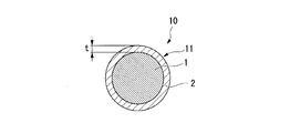
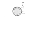
- FIG. 17 is a cross-sectional view showing a high-frequency electric wire 10 (hereinafter referred to as an electric wire 10) according to an embodiment of the present invention.
- the electric wire 10 shown here is an electric wire used in a specific frequency band, and is a conductor composed of a two-layer structure conductor provided with an inner layer 1 and an outer layer 2 formed so as to cover the outer peripheral surface of the inner layer 1. Part 11.
- the inner layer 1 is formed of a material having a lower conductivity than copper (a material having a higher volume resistivity than copper).
- a metal having a lower conductivity than copper can be used as a material of the inner layer 1.
- the material of the inner layer 1 may be an insulator.
- the material of the inner layer 1 may be a magnetic material or a nonmagnetic material.
- the inner layer 1 may have a circular cross-sectional shape.
- a cross section means a surface perpendicular
- the material of the inner layer for example, an aluminum-containing material, an iron-containing material, a nickel-containing material, and the like are suitable.
- the inner layer 1 is preferably made of a uniform material.
- the inner layer 1 may be a composite material composed of a plurality of materials. In that case, the conductivity (also referred to as electrical conductivity or electrical conductivity) is obtained based on the cross-sectional area ratio of the plurality of materials. Can do.
- aluminum-containing material aluminum (Al) or an aluminum alloy can be used.
- electrical aluminum (EC aluminum), Al—Mg—Si alloys (JIS6000 series), etc. can be used.
- a two-layer structure conductor in which the inner layer is made of an aluminum wire and the outer layer is made of copper is called a copper-covered aluminum wire.
- iron (Fe) or an iron alloy can be used as the iron-containing material.
- the iron alloy include a material containing one or more of carbon, silicon, nickel, tungsten, and chromium.
- a steel wire (steel wire), a stainless steel wire, or the like can be suitably used as the inner layer 1.
- a two-layer structure conductor whose inner layer is made of steel wire and whose outer layer is made of copper is called a copper-covered steel wire.
- nickel-containing material nickel, a nickel alloy, or the like can be used.
- Nickel alloys include nickel chromium alloys.
- a nichrome wire can be used as the inner layer 10.
- a two-layer structure conductor in which the inner layer is made of nichrome wire and the outer layer is made of copper is called a copper-covered nichrome wire.
- the inner layer 1 is not limited to the exemplified materials, and may be pure metal such as magnesium, tungsten, titanium, iron, brass, phosphor bronze, quartz bronze, copper / beryllium alloy, and copper / nickel / silicon alloy.
- a copper alloy such as Further, it may be an insulator such as rubber or plastic.
- the outer layer 2 is made of copper, and its cross-sectional area is desirably 50% or less with respect to the cross-sectional area of the entire conductor portion 11 including the inner layer 1 and the outer layer 2.
- the cross-sectional area ratio (the cross-sectional area ratio of the outer layer 2 with respect to the cross-sectional area of the entire conductor portion 11) can be set to 5% to 50%, for example. By making the cross-sectional area ratio of the outer layer 2 within this range, it contributes to the reduction of AC resistance.
- the outer layer 2 may have a constant thickness.
- the diameter of the entire electric wire 10 (the diameter of the conductor portion 11) can be set to 0.05 mm to 3.2 mm, for example.
- one or more insulating layers such as resin and enamel may be formed on the outer peripheral side of the outer layer in the high frequency electric wire of the present embodiment.
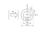
- FIG. 16A a two-layer structure conductor having a circular cross section, each layer made of a different material, and extending uniformly in the z-axis direction was modeled.
- Outer diameter the conductivity of the i-th layer of the layers from the inside, respectively relative permeability 2r i, sigma i, and mu i, the time factor and e j? T.
- ⁇ 0 represents the magnetic permeability in vacuum.
- i is a natural number.
- j is an imaginary unit
- FIG. 16B when a current having an amplitude I flows in the z-axis direction of the conducting wire, the z component E z of the electric field satisfies the following wave equation.
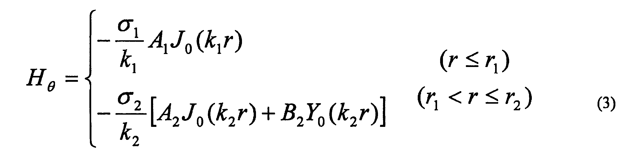
- equation (1) is a zero-order Bessel equation, it has the following solution.
- k i 2 is expressed by the following equation.
- k i 2 ⁇ j ⁇ 0 ⁇ i ⁇ i J n and Y n are n-order Bessel functions and Neumann functions, respectively, and A i and B i are constants determined by the following boundary conditions.
- the magnetic field H ⁇ represents the ⁇ direction component.
- ⁇ k 2 r 2 .
- a resistance R s and an internal inductance L i when an alternating current is passed through a two-layer structure conductor having a unit length are expressed by the following equations.
- the frequency of the alternating current is preferably a frequency within a specific frequency region defined (set) as a range in which the electric wire (product) is used.
- each layer is a magnetic material and exhibits magnetic loss due to magnetic hysteresis or the like
- the loss can be expressed by introducing an imaginary part into the magnetic permeability. For example, the following equation holds.
- Equation (8) has the following solution.
- C i and D i are constants determined by the following boundary conditions.
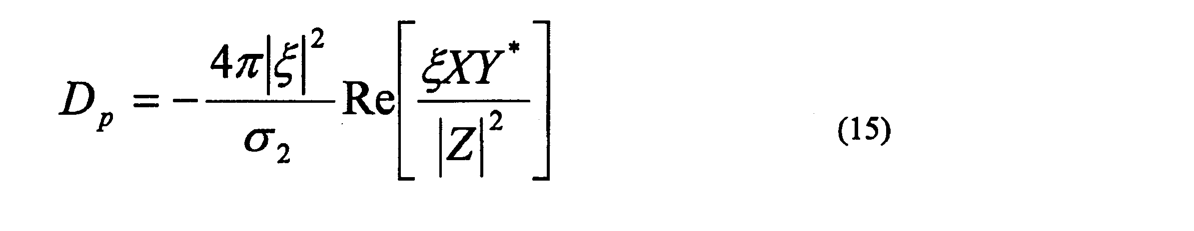
- the power consumption in the conducting wire is equal to the real part of the value obtained by integrating the pointing vector flowing in from the conducting wire surface on the conducting wire surface S. Therefore, when a magnetic field having an amplitude H 0 is applied, the time average of the eddy current loss generated in the conductor is expressed by the following equation.
- H 0 Since the magnetic field near the coil is generated by the current I flowing through the coil, the magnetic field amplitude H 0 is proportional to the amplitude of I. If this proportionality coefficient is ⁇ , H 0 is expressed as follows.
- D p is expressed as follows.
- Example 1 A two-layer structure conductor (copper-covered aluminum wire) (Example 1) in which the inner layer is formed of an alloy aluminum wire and the outer layer is formed of copper, and the two layers in which the inner layer is formed of a steel wire and the outer layer is formed of copper Regarding the structure conductor (copper-covered steel wire) (Example 2) and the two-layer structure conductor (copper-covered nichrome wire) (Example 3) in which the inner layer is formed of nichrome wire and the outer layer is formed of copper, the following Calculated. For comparison, the same calculation was performed for a copper wire having a single layer structure (single layer structure) (Comparative Example 1).
- the copper wire may be circular in cross section.
- a single layer structure means a structure made of a uniform material.
- the two-layer structure conductor or the copper wire may be simply referred to as “conductive wire”.
- the aluminum alloy is sometimes simply referred to as “aluminum”.
- the outer diameter of the conducting wires was 1.0 mm.
- the cross-sectional area ratio of the outer layer to the entire conductor was set to 25%.
- the resistance R s and the internal inductance L i shown in the above equation (5) were obtained by calculation. Moreover, was determined by calculating the D p shown in equation (15) described above.
- the volume resistivity (20 ° C.) of copper, alloy aluminum, steel, and nichrome is 1.72 ⁇ 10 ⁇ 8 [ ⁇ ⁇ m], 3.02 ⁇ 10 ⁇ 8 [ ⁇ ⁇ m], respectively. 1.57 ⁇ 10 ⁇ 7 [ ⁇ ⁇ m] and 1.50 ⁇ 10 ⁇ 6 [ ⁇ ⁇ m] were set.
- the volume resistivity of aluminum alloy was based on the JEC-3405a aluminum alloy electric wire standard of the Institute of Electrical Engineers of Japan.
- the electrical conductivity (20 ° C.) of copper, alloy aluminum, steel, and nichrome is 5.8 ⁇ 10 7 [ ⁇ ⁇ 1 ⁇ m ⁇ 1 ], 3.3 ⁇ 10 7 [ ⁇ ⁇ 1 ⁇ m ⁇ 1 ], respectively. , 6.4 ⁇ 10 6 [ ⁇ ⁇ 1 ⁇ m ⁇ 1 ] and 6.6 ⁇ 10 6 [ ⁇ ⁇ 1 ⁇ m ⁇ 1 ].
- the relative magnetic permeability of copper, alloy aluminum, steel, and nichrome was 1, 1, 100, and 1, respectively.
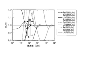
- Figure 1 shows the calculation results of the resistance R s.
- Comparative Example 1 copper wire
- Example 1 has a lower resistance Rs. That is, in the low-frequency side than the first frequency, carried out in the resistance R s is higher than the resistance R s of Comparative Example 1 (Copper), the first frequency of Examples 1-3 (two-layer structure conductive)
- the resistances R s of 1 to 3 and Comparative Example 1 are the same.
- Figure 2 shows the calculated results of the D p.
- Comparative Example 1 copper wire
- Example 1 to 3 double-layer structure conductor
- Comparative Example 1 copper wire
- FIG. 3 shows the calculation result of the internal inductance L i .
- Comparative Example 1 copper wire
- Comparative Example 1 copper wire
- Li was higher than. That is, in the low-frequency side than the first frequency, implemented in internal inductance L i is lower than L i of Comparative Example 1 (Copper), the first frequency of Examples 1-3 (two-layer structure conductive) Example L i and Comparative examples 1 and 1-3 match.
- FIG. 4 shows the ratio of the resistance R s of Examples 1 to 3 and Comparative Example 1 (Copper) (Examples 1-3 / Comparative Example 1)
- FIG. This figure shows the following.
- Example 1 copper clad aluminum wire
- Comparative Example 1 copper
- Example 2 copper-covered steel wire
- Example 3 Dokutsugae nichrome wire
- Example 3 Comparative Example 1 (copper)
- the resistance R s was reduced to about 7% at the maximum.
- FIG. 2 shows the ratio of D p of the Examples 1-3 and Comparative Example 1 (Copper) (Examples 1-3 / Comparative Example 1)
- FIG. This figure shows the following.
- Example 1 copper clad aluminum wire
- Comparative Example 1 Comparative Example 1
- Example 2 Yamatsugae steel wire
- Example 3 Determination of Comparative Example 1 (Copper)
- FIG. 6 shows the ratio of the internal inductance Li between Examples 1 to 3 and Comparative Example 1 (copper wire) (Examples 1 to 3 / Comparative Example 1) in order to make the calculation results shown in FIG. 3 easier to understand.
- FIG. This figure shows the following.
- Example 1 copper-covered aluminum wire
- Example 2 copper-covered steel wire
- Example 3 copper-covered nichrome wire
- the internal inductance Li was increased by up to about 2% compared to Comparative Example 1 (copper wire).
- Example 4 Other than that the cross-sectional area ratio of the outer layer is 75% in Example 2 and the same two-layer structure conductive (Dokutsugae steel wire), for Comparative Example 1 (copper), the ratio of R s, the ratio of D p, and to determine the ratio of L i.
- the results are shown in FIG. 7A.
- the ratio of R s to Comparative Example 1 (copper wire) is “R s (75% CS / Cu)”
- the ratio of D p is “D p (75% CS / Cu)”
- L i The ratio was described as “L i (75% CS / Cu)”.
- Example 2 also shows for Comparative Example 1 (copper), the ratio of R s, the ratio of D p, the ratio of L i in Figure 7A.
- Example 5 For except that the cross-sectional area ratio of the outer layer and 5% Example 2 the same two-layer structure conductive (Dokutsugae steel wire), for Comparative Example 1 (copper), the ratio of R s, the ratio of D p, to determine the ratio of L i.
- the results are shown in FIG. 7A.
- the ratio was described as “L i (5% CS / Cu)”.
- Example 4 As shown in FIG. 7A, in the frequency domain A1, R s of Example 4 (Dokutsugae steel wire) is less than R s of Comparative Example 1 (Copper). Therefore, in the frequency domain A1, relates R s, Example 4 is superior to Comparative Example 1. Further, in the frequency domain A1, the D p of Example 4 is smaller than the D p of Comparative Example 1 relates to D p, Example 4 is superior to Comparative Example 1. A region in the frequency domain A1, the narrow frequency area B1 from the frequency domain A1, greater than L i for the L i of Example 4 Comparative Example 1 relates to L i, to Example 4 Comparative Example 1 Is superior. Thus, in the frequency domain A1, Example 4 is superior with respect to R s and D p, the narrower frequency range than the area A1 B1, also becomes dominant with respect to L i.
- Example 2 is superior with respect to R s and D p, the narrower frequency range than the area A2 B2, also the advantage with respect to L i.
- the frequency domain A3, Example 5 is superior with respect to R s and D p, the narrower frequency range than the region A3 B3, also becomes dominant with respect to L i.
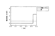
- FIG. 8A to 8C show a copper-covered nichrome wire (Example 3, cross-sectional area ratio of outer layer 25%, outer diameter 1.0 mm), frequency 1 kHz (FIG. 8A), 3 MHz (FIG. 8B), or 10 MHz (FIG. 8C). It is a figure which shows the real part of the current density distribution of the radial direction of a copper clad nichrome wire at the time of flowing the electric current of. The current density distribution was similarly calculated for Comparative Example 1 (copper wire). This current density distribution was calculated by multiplying equation (2) by the conductivity.
- the resistance in a specific frequency region can be suppressed more than the copper wire. Therefore, the Q value of the coil can be improved.
- FIGS. 9A to 9C show a conductive wire perpendicular to an external magnetic field when a uniform magnetic field is applied to a copper-covered nichrome wire (Example 3, cross-sectional area ratio of outer layer 25%, outer diameter 1.0 mm) from the outside ( It is a figure which shows the absolute value of the eddy current density of the surface which passes along the center of a copper covering nichrome wire.
- 9A shows the absolute value of the eddy current density when the frequency of the magnetic field is 500 kHz
- FIG. 9B shows the absolute value of the eddy current density when the frequency of the magnetic field is 2 MHz
- FIG. 9C shows the case where the frequency of the magnetic field is 10 MHz.
- the absolute value of the eddy current density was similarly calculated. This current density distribution was calculated by multiplying Equation (11) by the conductivity.
- FIG. 9A it can be seen that at 500 kHz, the eddy current in the copper-covered nichrome wire flows to the outer layer, and thus the current density distribution in the copper-covered nichrome wire is more strongly biased than in the copper wire.
- FIG. 9B at 2 MHz, the current density on the surface of the conductive wire is larger in the copper wire than in the copper-covered nichrome wire, and therefore the current density distribution of the copper wire is more biased than in the copper-covered nichrome wire. I understand.
- FIG. 9C it can be seen that at 10 MHz, the current density distribution of the copper nichrome wire is close to the current density distribution of the copper wire.
- the eddy current deviation of the copper wire is larger than the eddy current deviation of the copper-covered nichrome wire, so the loss of the copper nichrome wire is smaller than that of the copper wire.
- the outer layer is made of copper and the inner layer is made of a material having a lower conductivity than copper (a material having a high volume resistivity)
- the eddy current loss in a specific frequency region is reduced by copper wire. Than can be suppressed.
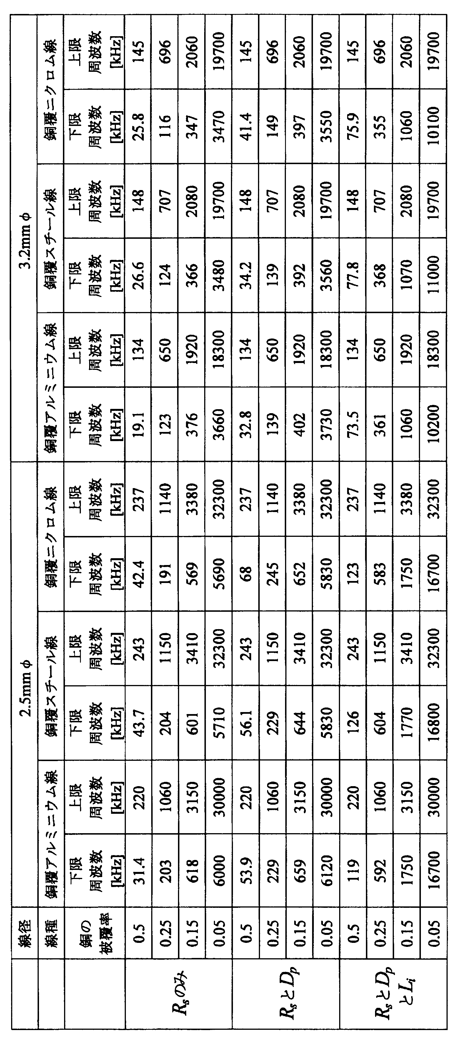
- Example 6 Copper-clad aluminum wire (Example 6), copper-clad steel wire (Example 7), and copper-clad nichrome wire (Example 8), which are two-layer structure conductors having an outer diameter of 0.1 mm, 1.0 mm, or 3.2 mm
- the frequency region in which the resistance R s is smaller than the resistance R s of the copper wire was obtained by simulation.
- the cross-sectional area ratio of the outer layer was 5%, 15%, 25%, and 50%.
- the lower limit value and upper limit value of the frequency domain are shown in FIGS. 10A to 10C.
- FIGS. 10A to 10C show the results when the outer diameter is 0.1 mm, 1.0 mm, and 3.2 mm, respectively.
- Example 6 Copper clad aluminum wire (Example 6), Dokutsugae steel wire (Example 7), Dokutsugae nichrome wire (Example 8), R s is smaller than R s of copper, and D p is the copper wire D
- R s is smaller than R s of copper
- D p is the copper wire D
- FIGS. 11A to 11C show the results when the outer diameter is 0.1 mm, 1.0 mm, and 3.2 mm, respectively.
- the cross section area ratio of the outer layer (copper) is changed, the two-layer structure conductors R s is smaller than R s of copper, and two-layer structure conductors D p copper wire D
- the frequency region smaller than p changes. Therefore, by adjusting the cross-sectional area ratio of the outer layer (copper), the resistance and proximity effect of the two-layer structure conductor can be reduced over the copper wire in a wide frequency region. Therefore, the Q value of the coil can be further improved.
- Example 6 Copper clad aluminum wire (Example 6), Dokutsugae steel wire (Example 7), Dokutsugae nichrome wire (Example 8), R s is smaller than R s of copper, and D p is the copper wire D smaller than p, moreover obtained by simulating a larger frequency range than the internal inductance L i of internal inductance L i copper wire.
- the lower limit value and upper limit value of the frequency domain are shown in FIGS. 12A to 12C. 12A to 12C show the results when the outer diameter is 0.1 mm, 1.0 mm, and 3.2 mm, respectively.
- Tables 1 to 3 show (1) resistance R s of copper wire resistance R for copper-clad aluminum wire (Example 6), copper-clad steel wire (Example 7), and copper-clad nichrome wire (Example 8). lower limit and the upper limit of the smaller becomes the frequency domain than s, (2) R s is smaller than R s of copper, and lower and upper limits of the smaller becomes the frequency domain than the D p of D p is copper, (3 ) R s is smaller than R s of copper, and D p is smaller than D p of copper, moreover internal inductance L i is the lower limit and the upper limit value of the larger frequency range than the internal inductance L i of copper, Indicates.
- Two-layer structure conductive of R s, D p, L i is copper R s, D p, different from the L i, since the electrical conductivity is less likely current flows through the lower inner layer, the current distribution due to the skin effect This is because the two-layer structure conductor and the copper wire are different.
- the lower limit frequency and the upper limit frequency of the above-described frequency region can be determined in association with the skin thickness ⁇ [m] of the reference copper wire.
- the “reference copper wire” has a conductor portion made of pure copper (formed only of pure copper).
- the copper wire preferably has the same wire diameter as the two-layer structure conductor, but may have a different wire diameter.
- FIG. 13 shows the ratio between the skin thickness ⁇ of the copper wire and the radius r 2 of the two-layer structure conductor at the lower limit frequency and the upper limit frequency in the frequency region where R s of the two-layer structure conductor is lower than R s of the copper wire. indicates the ratio of the radius r 2 of the thickness t and the two-layer structure conductive two-layered conductor layer (copper), the correlation.
- a solid line is a regression analysis line for the lower limit frequency
- a broken line is a regression analysis line for the upper limit frequency.
- the skin thickness ⁇ [m] in the copper wire is expressed by the following formula (18).
- the thickness t of the outer layer (copper) of the two-layer structure conductor is 0.92 times the skin thickness ⁇ of the copper wire, and at the upper limit frequency, the thickness t is equal to the skin thickness ⁇ . It became 0.37 times. Therefore, when the outer layer thickness t of the (copper) [m] is in the range of the following equation (19), R s two-layered conductor is lower than R s of copper. Therefore, the Q value of the coil can be improved.
- the thickness t of the outer layer (copper) of the two-layer structure conductor is 0.76 times the skin thickness ⁇ of the copper wire, and at the upper limit frequency, the thickness t is equal to the skin thickness ⁇ . It became 0.37 times. Therefore, when the thickness t of the outer layer (copper) [m] is in the range of the following equation (21), the two-layer structure conductive R s is smaller than R s of copper, and D p is the copper wire smaller than D p. Therefore, the Q value of the coil can be further improved.
- two-layer structure conductors R s is lower than R s of copper, and D p of the two-layer structure conductive is smaller than D p of copper, moreover L i is than L i Copper
- the ratio of the skin thickness ⁇ of the copper wire to the radius r 2 of the two-layer structure conductor, the thickness t of the outer layer (copper) of the two-layer structure conductor, and the two-layer structure at the lower limit frequency and the upper limit frequency The correlation with the ratio of the radius r 2 of the conductor is shown.
- a solid line is a regression analysis line for the lower limit frequency
- a broken line is a regression analysis line for the upper limit frequency.
- the thickness t of the outer layer (copper) of the two-layer structure conductor is 0.51 times the skin thickness ⁇ of the copper wire, and at the upper limit frequency, the thickness t is equal to the skin thickness ⁇ . It became 0.37 times. Therefore, when the thickness t of the outer layer (copper) [m] is in the range of the following equation (23), the two-layer structure conductive R s is smaller than R s of copper, and D p is the copper wire becomes smaller than D p, moreover L i is larger than L i of copper. Therefore, the Q value of the coil can be further improved.
- the frequency of current flowing in a cable or coil is determined by an external factor such as a device in which the cable or coil is used.
- the equipment used include an induction heating device, a non-contact power feeding device, a plasma generator, a switching power supply, a microwave filter, an antenna, and facilities associated therewith.
- the thickness of the conductor is determined by a size factor, a balance between R s and D p , and the like.
- the resistance can be reduced as compared with the copper wire by selecting the thickness and the cross-sectional area ratio of the outer layer (copper) according to the equation (19).
- the resistance and the proximity effect can be reduced more than the copper wire by selecting the thickness and the cross-sectional area ratio of the outer layer (copper) according to the equation (21). Further, when increasing the Q value of the coil, the apparent power with respect to the power consumption of the coil can be increased by selecting the thickness and cross-sectional area ratio of the outer layer (copper) according to the equation (23).
- the electric wire of the present invention has a structure in which the outer layer is made of copper and the inner layer is made of a material having a lower conductivity than copper (a material having a high volume resistivity. For example, a metal or an insulator having a lower conductivity than copper).
- the constituent material of the inner layer is not limited to the exemplified materials.
- FIG. 18 shows an electric wire 10 ⁇ / b> A that is a modification of the electric wire 10.
- the insulating coating layer 3 that covers the outer peripheral surface of the conductor portion 11 is provided on the outer peripheral surface of the conductor portion 11 (the outer peripheral surface of the outer layer 2).
- the insulating coating layer 3 is the outermost layer of the electric wire 10A.
- the insulating coating layer 3 can be formed by applying an enamel paint such as polyester, polyurethane, polyimide, polyesterimide, or polyamideimide.
- the electric wire 10A in which the insulating coating layer 3 is formed by the enamel paint is an enameled wire.
- FIG. 19 shows a litz wire 60 which is an example of a litz wire using the electric wire 10A shown in FIG.
- the litz wire 60 is configured by bundling a plurality of electric wires 10A and twisting them together.
- FIG. 20 shows a cable 80 which is an example of a cable in which an insulation coating is applied to the litz wire 60.
- the cable 80 is provided with an insulating coating layer 81 formed of polyethylene or the like on the outer peripheral surface of the litz wire 60.
- FIG. 21 shows a coil 70 which is an example of a coil (high frequency coil) using the electric wire 10A shown in FIG.
- the coil 70 includes an electric wire 10 ⁇ / b> A and a support body 73 having a body portion 71 and flange portions 72 formed at both ends thereof.
- the electric wire 10 ⁇ / b> A is wound around the trunk portion 71.
- a litz wire 60 shown in FIG. 19 or a cable 80 may be used instead of the electric wire 10A.
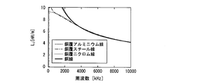
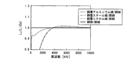
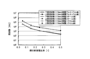
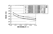
- Example 9 A coil (number of turns 3) was prepared using a copper-covered aluminum wire (outer layer cross-sectional area ratio 25%, outer diameter 1.8 mm), and AC resistance was measured. The results are shown in FIG. For comparison, the same calculation was performed for a copper wire having a single layer structure (Comparative Example 2). In the figure, the copper-clad aluminum wire is described as “CA”, and the copper wire is described as “Cu”. The ratio of R s (copper clad aluminum wire / copper) was evaluated as "CA / Cu”. As shown in FIG.
- Example 10 A coil (number of turns 1) was prepared using a copper-clad steel wire (cross-sectional area ratio of outer layer: 25%, outer diameter: 2.0 mm), and AC resistance was measured. The results are shown in FIG. In the figure, the copper-clad steel wire is described as “CS”, and the copper wire is described as “Cu”. The ratio of Rs (copper-covered steel wire / copper wire) was defined as “CS / Cu”. As shown in FIG. 23, in the frequency domain A5, R s of Example 10 (Dokutsugae steel wire) falls below the R s in Comparative Example 2 (Copper), the ratio of R s is smaller than 1.
- an outer layer made of copper is formed on the outer peripheral surface of the inner layer body by performing TIG welding or plasma welding or the like by vertically attaching copper tape to the surface of the inner layer body made of aluminum alloy, steel, nichrome alloy or the like.
- Use as a base material By drawing this base material through a plurality of drawing dies, an electric wire 10 having an inner layer 1 and an outer layer 2 can be obtained.
- the inner layer 1 is obtained by drawing a base material obtained by inserting an inner layer body formed of an aluminum alloy or the like into a copper tube produced by a general-purpose pipe making method using a plurality of wire drawing dies.
- the electric wire 10 having the outer layer 2 can be obtained.
- the outer layer 2 may be formed on the outer peripheral surface of the inner layer 1 by copper plating.
- the manufacturing method shown here does not limit the scope of the present invention.
- the high-frequency electric wire according to the embodiment of the present invention can be manufactured by a manufacturing method other than the method exemplified here.
- the above embodiments exemplify apparatuses and methods for embodying the technical idea of the present invention.
- the technical idea of the present invention is based on the material, shape, structure, arrangement, etc. of the component parts. Not specific.
- the present invention does not exclude the structure having the third layer in addition to the inner layer and the outer layer. Further, the least square method may be employed for the regression analysis using the above-mentioned linear function.
- the high-frequency electric wire and high-frequency coil of the present invention include a high-frequency transformer, a motor, a reactor, a choke coil, an induction heating device, a magnetic head, a high-frequency power supply cable, a DC power supply unit, a switching power supply, an AC adapter, and an eddy current detection method.
- the present invention can be used in the electronic equipment industry including the manufacturing industry of various devices such as non-contact power supply devices or high-frequency current generators such as displacement sensors / flaw detection sensors, IH cooking heaters, coils, and power supply cables.
Landscapes
- Engineering & Computer Science (AREA)
- Power Engineering (AREA)
- Non-Insulated Conductors (AREA)
- Insulated Conductors (AREA)
- Coils Of Transformers For General Uses (AREA)
- Communication Cables (AREA)
Abstract
Description
本願は、2013年12月2日に、日本に出願された特願2013-249685号に基づき優先権を主張し、その内容をここに援用する。
表皮効果および近接効果を抑制する対策としては、素線の細径化、および各素線を絶縁被覆したリッツ線の採用などがある(特許文献1~3を参照)。
しかし、リッツ線を採用しても、素線の細径化による表皮効果および近接効果を抑制することには限界がある。また、高周波では近接効果による抵抗増大が起こりやすいという問題を解決できない。
また、特許文献4、非特許文献1および非特許文献2には、銅線に磁性層を被覆形成することで、銅線内部への磁界の入り込みを抑制し近接効果を低減する構造が提案されている。しかしながら、この構造では、磁性層に電流が集中するため、高周波では表皮効果が増大するという問題がある。
特許文献6には、銅被覆アルミニウム線が開示されている。しかし、銅被覆アルミニウム線では、同じ線径の銅線と比較して、交流抵抗を低くするのは難しい。
前記外層の厚さtは、1.3δ<t<2.7δを満たしてもよい。
前記外層の厚さtは、2.0δ<t<2.7δを満たしてもよい。
前記導体部の外周面には、絶縁被覆層が設けられてもよい。
本発明の第2態様に係る高周波用コイルは、上記第1態様に係る高周波用電線を備える。
本発明の第3態様に係るリッツ線は、複数撚り合わされた上記第1態様に係る高周波用電線を備える。
本発明の第4態様に係るケーブルは、絶縁被覆が施された上記第3態様に係るリッツ線を備える。
本発明の第5態様に係るコイルは、上記第3態様に係るリッツ線または上記第4態様に係るケーブルを備える。
図17は、本発明の一実施形態に係る高周波用電線10(以下、電線10という)を示す断面図である。
ここに示す電線10は、特定の周波数帯域で使用される電線であって、内層1と、内層1の外周面を被覆して形成された外層2と、を備えた二層構造導体からなる導体部11を有する。
なお、本実施形態において断面とは、導体部11の軸方向に対して垂直な面をいう。
内層1は均一材料からなることが望ましい。内層1は複数の材料からなる複合材であってもよいが、その場合には、導電率(電気伝導率、電気伝導度ともいう)は、前記複数の材料の断面積比に基づいて求めることができる。
内層がアルミニウム線からなり、外層が銅からなる二層構造導体を、銅覆アルミニウム線と呼ぶ。
内層がスチール線からなり、外層が銅からなる二層構造導体を、銅覆スチール線と呼ぶ。
ニッケル合金としては、ニッケルクロム系合金がある。この場合、例えば、内層10としてニクロム線が使用できる。
内層がニクロム線からなり、外層が銅からなる二層構造導体を、銅覆ニクロム線と呼ぶ。
外層2は、一定厚さであってもよい。
電線10全体の直径(導体部11の直径)は、例えば0.05mm~3.2mmとすることができる。
図16Aに示すように、断面が円形であって、各層が互いに異なる素材で構成され、z軸方向に一様に延在する二層構造導体をモデル化した。内側からi層目の層の外径、導電率、比透磁率をそれぞれ2ri、σi、μiとし、時間因子をejωtとする。μ0は真空中の透磁率を表す。iは自然数である。また、jは虚数単位であり、ωはfを周波数とした場合にω=2πfで規定される角周波数である。
図16Bに示すように、この導線のz軸方向に振幅Iの電流を流したとき、電界のz成分Ezは、次の波動方程式を満たす。


またJn,Ynはそれぞれn次のベッセル関数とノイマン関数とであり、Ai,Biは次の境界条件により決定される定数である。


交流電流を単位長さの二層構造導体に通電したときの抵抗Rsおよび内部インダクタンスLiは、次の式で表される。
なお、前記交流電流の周波数は、その電線(製品)が使用される範囲として規定(設定)された、特定の周波数領域内の周波数であることが望ましい。


図16Aに示すように、H=∇×Aを満たすベクトルポテンシャルを導入すると、z軸方向のベクトルポテンシャルA2=H0rsinθは、x軸方向からの一様な振幅H0の磁界を与える。
導線にこの磁界を作用させたとき、Azは以下の波動方程式を満たす。


内層が合金アルミニウム線で形成され、外層が銅で形成される二層構造導体(銅覆アルミニウム線)(実施例1)と、内層がスチール線で形成され、外層が銅で形成される二層構造導体(銅覆スチール線)(実施例2)と、内層がニクロム線で形成され、外層が銅で形成される二層構造導体(銅覆ニクロム線)(実施例3)とについて、以下の計算を行った。
比較のため、単層構造(一層構造)の銅線についても同様の計算を行った(比較例1)。銅線は断面円形としてよい。単層構造とは均一材料からなる構造をいう。
以下の説明において、二層構造導体または銅線を、単に「導線」ということがある。また、合金アルミニウムを単に「アルミニウム」ということがある。
導線(実施例1~3および比較例1)の外径は1.0mmとした。また、実施例1~3(二層構造導体)では、導線の全体に対する外層の断面積比率は25%とした。
なお、計算にあたり、銅、合金アルミニウム、スチール、及びニクロムの体積抵抗率(20℃)をそれぞれ1.72×10⁻⁸[Ω・m]、3.02×10⁻⁸[Ω・m]、1.57×10⁻⁷[Ω・m]、及び1.50×10⁻⁶[Ω・m]とした。なお、合金アルミニウムの体積抵抗率は、電気学会電気規格調査会標準規格JEC-3405イ号アルミ合金電線を参考にした。銅、合金アルミニウム、スチール、及びニクロムの導電率(20℃)は、それぞれ5.8×10⁷[Ω-1・m-1]、3.3×10⁷[Ω-1・m-1]、6.4×10⁶[Ω-1・m-1]、及び6.6×10⁶[Ω-1・m-1]とした。
銅、合金アルミニウム、スチール、及びニクロムの比透磁率は、それぞれ1、1、100、及び1とした。
すなわち、第1の周波数よりも低周波側では、実施例1~3(二層構造導体)の抵抗Rsは比較例1(銅線)の抵抗Rsより高く、第1の周波数において実施例1~3と比較例1との抵抗Rsは一致する。そして、第1の周波数よりも高周波側でかつ第2の周波数未満の範囲では実施例1~3の抵抗Rsは比較例1の抵抗Rsより低く、第2の周波数において実施例1~3と比較例1との抵抗Rsは再び一致し、第2の周波数よりも高周波側では実施例1~3の抵抗Rsは比較例1の抵抗Rsより高くなった。
すなわち、第1の周波数よりも低周波側では、実施例1~3(二層構造導体)のDpは比較例1(銅線)のDpより高く、第1の周波数において実施例1~3と比較例1とのDpは一致する。そして、第1の周波数よりも高周波側でかつ第2の周波数未満の範囲では実施例1~3のDpは比較例1のDpより低く、第2の周波数において実施例1~3と比較例1とのDpは再び一致し、第2の周波数よりも高周波側では実施例1~3のDpは比較例1のDpより高くなった。
すなわち、第1の周波数よりも低周波側では、実施例1~3(二層構造導体)の内部インダクタンスLiは比較例1(銅線)のLiより低く、第1の周波数において実施例1~3と比較例1とのLiは一致する。そして、第1の周波数よりも高周波側でかつ第2の周波数未満の範囲では実施例1~3のLiは比較例1のLiより高くなり、第2の周波数において実施例1~3と比較例1とのLiは再び一致し、第2の周波数よりも高周波側では実施例1~3のLiは比較例1のLiより低くなった。
実施例1(銅覆アルミニウム線)では、比較例1(銅線)に対し、抵抗Rsを最大で約1%低減できた。
実施例2(銅覆スチール線)では、比較例1(銅線)に対し、抵抗Rsを最大で約7%低減できた。
実施例3(銅覆ニクロム線)では、比較例1(銅線)に対し、抵抗Rsを最大で約7%低減できた。
実施例1(銅覆アルミニウム線)では、比較例1(銅線)に対し、Dpを最大で約1%低減できた。
実施例2(銅覆スチール線)では、比較例1(銅線)に対し、Dpを最大で約7%低減できた。
実施例3(銅覆ニクロム線)では、比較例1(銅線)に対し、Dpを最大で約7%低減できた。
実施例1(銅覆アルミニウム線)では、比較例1(銅線)に対し、内部インダクタンスLiを最大で約0.3%高くできた。
実施例2(銅覆スチール線)では、比較例1(銅線)に対し、内部インダクタンスLiを最大で約2%高くできた。
実施例3(銅覆ニクロム線)では、比較例1(銅線)に対し、内部インダクタンスLiを最大で約2%高くできた。
外層の断面積比率を75%としたこと以外は実施例2と同様の二層構造導体(銅覆スチール線)について、比較例1(銅線)に対する、Rsの比、Dpの比、およびLiの比を求めた。結果を図7Aに示す。
図7A中、比較例1(銅線)に対するRsの比を「Rs(75%CS/Cu)」とし、Dpの比を「Dp(75%CS/Cu)」とし、Liの比を「Li(75%CS/Cu)」と記載した。
図中、比較例1(銅線)に対するRsの比を「Rs(25%CS/Cu)」とし、Dpの比を「Dp(25%CS/Cu)」とし、Liの比を「Li(25%CS/Cu)」と記載した。
外層の断面積比率を5%としたこと以外は実施例2と同様の二層構造導体(銅覆スチール線)について、比較例1(銅線)に対する、Rsの比、Dpの比、Liの比を求めた。結果を図7Aに示す。
図7A中、比較例1(銅線)に対するRsの比を「Rs(5%CS/Cu)」とし、Dpの比を「Dp(5%CS/Cu)」とし、Liの比を「Li(5%CS/Cu)」と記載した。
また、周波数領域A1では、実施例4のDpは比較例1のDpより小さいため、Dpに関し、実施例4は比較例1に対して優位である。
周波数領域A1内の領域であって、周波数領域A1より狭い周波数領域B1では、実施例4のLiは比較例1のLiより大きいため、Liに関し、実施例4は比較例1に対して優位である。
このように、周波数領域A1では、実施例4はRsとDpに関して優位であり、領域A1より狭い周波数領域B1では、Liに関しても優位となる。
図7Cに示すように、周波数領域A3では、実施例5はRsとDpに関して優位であり、領域A3より狭い周波数領域B3では、Liに関しても優位となる。
図8A~8Cは、銅覆ニクロム線(実施例3、外層の断面積比率25%、外径1.0mm)に、周波数が1kHz(図8A)、3MHz(図8B)、または10MHz(図8C)の電流を流した場合の、銅覆ニクロム線の半径方向の電流密度分布の実部を示す図である。
比較例1(銅線)についても、同様に電流密度分布を計算した。
この電流密度分布は、式(2)に導電率を乗じることによって計算した。
損失は電流の二乗関数であるので、電流分布の偏りが大きいほど損失が大きくなる。このため、銅覆ニクロム線は、銅線よりも抵抗が大きくなる。
銅線では還流が起こるため、正方向の電流は強く偏るために、銅覆ニクロム線に比べ、抵抗が大きくなる。
図9Aは磁界の周波数が500kHzである場合、図9Bは磁界の周波数が2MHzである場合、図9Cは磁界の周波数が10MHzである場合の渦電流密度の絶対値を示す。
比較例1(銅線)についても、同様に渦電流密度の絶対値を計算した。
この電流密度分布は、式(11)に導電率を乗じることによって計算した。
図9Bより、2MHzでは、導線の表面における電流密度は、銅覆ニクロム線よりも銅線のほうが大きいことから、銅線の方が、銅覆ニクロム線よりも電流密度分布が強く偏っていることがわかる。
図9Cより、10MHzでは、銅ニクロム線の電流密度分布は銅線の電流密度分布に近くなることがわかる。
これらの結果から、2MHzを含む周波数領域では、銅線の渦電流の偏りが、銅覆ニクロム線の渦電流の偏りよりも大きくなるため、銅線より銅ニクロム線のほうが、損失が小さくなることがわかった。
外径0.1mm、1.0mm、または3.2mmの二層構造導体である銅覆アルミニウム線(実施例6)、銅覆スチール線(実施例7)、銅覆ニクロム線(実施例8)において、抵抗Rsが銅線の抵抗Rsより小さくなる周波数領域をシミュレーションにより求めた。
外層の断面積比率は、5%、15%、25%、50%とした。
前記周波数領域の下限値と上限値を図10A~10Cに示す。
図10A~10Cは、それぞれ外径0.1mm、1.0mm、および3.2mmの場合の結果である。
前記周波数領域の下限値と上限値を図11A~11Cに示す。
図11A~11Cは、それぞれ外径0.1mm、1.0mm、および3.2mmの場合の結果である。
前記周波数領域の下限値と上限値を図12A~12Cに示す。
図12A~12Cは、それぞれ外径0.1mm、1.0mm、および3.2mmの場合の結果である。
このため、外層(銅)の断面積比率を調整することによって、広い周波数領域で、銅線よりも二層構造導体の抵抗および近接効果を低減し、かつ内部インダクタンスを大きくすることができる。
従って、コイルのQ値をさらに向上させることができる。


上述の周波数領域の下限周波数および上限周波数は、基準となる銅線における表皮厚さδ[m]に関連づけて定めることができる。
「基準とする銅線」は、純銅からなる(純銅のみで形成される)導体部を有する。銅線は、二層構造導体と同じ線径が好ましいが、異なる線径であってもよい。
これらの結果について1次関数で回帰分析を行ったところ、図13に示す回帰分析直線が得られた。実線は下限周波数についての回帰分析直線であり、破線は上限周波数についての回帰分析直線である。
δ=√(2/ωσμ) (18)
(ω:電流の角周波数(=2πf)、μ:銅線の透磁率[H/m]、σ:銅線の導電率[Ω-1m-1]、f:周波数[Hz])
このため、外層(銅)の厚さt[m]が以下の式(19)の範囲にあるとき、二層構造導体のRsは銅線のRsよりも低くなる。従って、コイルのQ値を向上させることができる。
1.1δ<t<2.7δ (19)
式(18)より、銅の導電率を5.8×10⁷[Ω-1・m-1]、銅の透磁率を真空の透磁率と等しい4π×10-7[H/m]とおけば、式(19)で与えられるt[m]は周波数f[Hz]に依存する関係式として、以下の式(20)のように表される。
86×10-3×f-0.5<t<178×10-3×f-0.5 (20)
これらの結果について1次関数で回帰分析を行ったところ、図14に示す回帰分析直線が得られた。実線は下限周波数についての回帰分析直線であり、破線は上限周波数についての回帰分析直線である。
このため、外層(銅)の厚さt[m]が以下の式(21)の範囲にあるとき、二層構造導体のRsは銅線のRsより小さく、かつDpは銅線のDpより小さくなる。従って、コイルのQ値をさらに向上させることができる。
1.3δ<t<2.7δ (21)
式(18)より、銅の導電率を5.8×10⁷[Ω-1・m-1]、銅の透磁率を真空の透磁率に等しい4π×10-7[H/m]とおけば、式(21)で与えられるt[m]は周波数f[Hz]に依存する関係式として、以下の式(22)のように表される。
86×10-3×f-0.5<t<178×10-3×f-0.5 (22)
これらの結果について1次関数で回帰分析を行ったところ、図15に示す回帰分析直線が得られた。実線は下限周波数についての回帰分析直線であり、破線は上限周波数についての回帰分析直線である。
このため、外層(銅)の厚さt[m]が以下の式(23)の範囲にあるとき、二層構造導体のRsは銅線のRsより小さく、かつDpは銅線のDpより小さくなり、しかもLiは銅線のLiよりも大きくなる。従って、コイルのQ値をさらに向上させることができる。
2.0δ<t<2.7δ (23)
式(18)より、銅の導電率を5.8×10⁷[Ω-1・m-1]、銅の透磁率を真空の透磁率に等しい4π×10-7[H/m]とおけば、式(23)で与えられるt[m]は周波数f[Hz]に依存する関係式として、以下の式(24)のように表される。
132×10-3×f-0.5<t<178×10-3×f-0.5 (24)
周波数が決定されたときに、導線の太さはサイズ的な要因や、RsとDpのバランスなどによって決定される。また、周波数と導線の太さが決まれば、外層(銅)の厚さおよび断面積比率を式(19)にしたがって選ぶことで、銅線よりも抵抗を低減することができる。
また、コイルのQ値を大きくする場合には、式(23)にしたがって外層(銅)の厚さおよび断面積比率を選ぶことで、コイルの消費電力に対する皮相電力を大きくすることができる。
絶縁被覆層3は、ポリエステルや、ポリウレタン、ポリイミド、ポリエステルイミド、ポリアミドイミド等のエナメル塗料を塗布することにより形成することができる。エナメル塗料により絶縁被覆層3を形成した電線10Aは、エナメル線である。
図19は、図18に示す電線10Aを用いたリッツ線の例であるリッツ線60を示す。リッツ線60は、電線10Aを複数本束ねて撚り合わせることにより構成されている。
図20は、リッツ線60に絶縁被覆が施されたケーブルの例であるケーブル80を示す。ケーブル80は、リッツ線60の外周面に、ポリエチレンなどで形成される絶縁被覆層81が設けられている。
図21は、図18に示す電線10Aを用いたコイル(高周波用コイル)の例であるコイル70を示す。コイル70は、電線10Aと、胴部71及びその両端に形成された鍔部72を有する支持体73とを備える。
電線10Aは、胴部71に巻きつけられている。
コイル70では、電線10Aに代えて、図19に示すリッツ線60を用いてもよいし、ケーブル80を用いてもよい。
銅覆アルミニウム線(外層の断面積比率25%、外径1.8mm)を用いてコイル(巻き数3)を作製し、交流抵抗を測定した。結果を図22に示す。
比較のため、単層構造の銅線についても同様の計算を行った(比較例2)。
図中、銅覆アルミニウム線を「CA」と記載し、銅線を「Cu」と記載した。Rsの比(銅覆アルミニウム線/銅線)を「CA/Cu」とした。
図22に示すように、周波数領域A4において、実施例9(銅覆アルミニウム線)のRsが比較例2(銅線)のRsを下回り、Rsの比(銅覆アルミニウム線/銅線)(CA/Cu)が1より小さくなった。
銅覆スチール線(外層の断面積比率25%、外径2.0mm)を用いてコイル(巻き数1)を作製し、交流抵抗を測定した。結果を図23に示す。
図中、銅覆スチール線を「CS」と記載し、銅線を「Cu」と記載した。Rsの比(銅覆スチール線/銅線)を「CS/Cu」とした。
図23に示すように、周波数領域A5において、実施例10(銅覆スチール線)のRsが比較例2(銅線)のRsを下回り、Rsの比が1より小さくなった。
次に、電線10の製造方法の一例について説明する。
例えば、アルミニウム合金や、スチール、ニクロム合金などからなる内層体の表面に、銅テープを縦添えしてTIG溶接又はプラズマ溶接等を行うことにより、内層体の外周面に銅からなる外層を形成し母材とする。この母材を複数段の伸線ダイスを通して伸線することによって、内層1と外層2とを有する電線10を得ることができる。
外層2は、内層1の外周面に銅めっきによって形成してもよい。
なお、ここに示す製造方法は本発明の範囲を限定するものではない。本発明の実施の形態に係る高周波用電線は、ここに例示した方法以外の製造方法により製造することもできる。
Claims (8)
- 銅よりも導電率が低い材料で形成される内層と、前記内層を被覆しかつ銅で形成される外層とを備えた導体部を有する高周波用電線であって、
前記高周波用電線が使用される交流電流の周波数の範囲において、純銅からなる導体部を備える銅線における表皮厚さδ[m]をδ=√(2/ωσμ)と規定した場合に、前記外層の厚さt[m]は、1.1δ<t<2.7δを満たす高周波用電線。ここで、ωは2πfで表される電流の角周波数、μは銅線の透磁率[H/m]、σは銅線の導電率[Ω-1m-1]、fは周波数[Hz]である。 - 前記外層の厚さtは、1.3δ<t<2.7δを満たす請求項1に記載の高周波用電線。
- 前記外層の厚さtは、2.0δ<t<2.7δを満たす請求項1または2に記載の高周波用電線。
- 前記導体部の外周面に、絶縁被覆層が設けられる請求項1~3のうちいずれか1項に記載の高周波用電線。
- 請求項4に記載の高周波用電線を備える高周波用コイル。
- 複数撚り合わされた請求項4に記載の高周波用電線を備えるリッツ線。
- 絶縁被覆が施された請求項6に記載のリッツ線を備えるケーブル。
- 請求項6に記載のリッツ線または請求項7に記載のケーブルを備えるコイル。
Priority Applications (5)
| Application Number | Priority Date | Filing Date | Title |
|---|---|---|---|
| JP2015551424A JP6194369B2 (ja) | 2013-12-02 | 2014-10-24 | 高周波用電線およびコイル |
| US15/100,765 US20160307666A1 (en) | 2013-12-02 | 2014-10-24 | High-frequency wire and coil |
| CN201480065335.XA CN105793932A (zh) | 2013-12-02 | 2014-10-24 | 高频用电线以及线圈 |
| EP14867830.3A EP3079158A4 (en) | 2013-12-02 | 2014-10-24 | High-frequency electrical wire and coil |
| KR1020167011803A KR20160065959A (ko) | 2013-12-02 | 2014-10-24 | 고주파용 전선 및 코일 |
Applications Claiming Priority (2)
| Application Number | Priority Date | Filing Date | Title |
|---|---|---|---|
| JP2013-249685 | 2013-12-02 | ||
| JP2013249685 | 2013-12-02 |
Publications (1)
| Publication Number | Publication Date |
|---|---|
| WO2015083456A1 true WO2015083456A1 (ja) | 2015-06-11 |
Family
ID=53273231
Family Applications (1)
| Application Number | Title | Priority Date | Filing Date |
|---|---|---|---|
| PCT/JP2014/078345 WO2015083456A1 (ja) | 2013-12-02 | 2014-10-24 | 高周波用電線およびコイル |
Country Status (6)
| Country | Link |
|---|---|
| US (1) | US20160307666A1 (ja) |
| EP (1) | EP3079158A4 (ja) |
| JP (1) | JP6194369B2 (ja) |
| KR (1) | KR20160065959A (ja) |
| CN (1) | CN105793932A (ja) |
| WO (1) | WO2015083456A1 (ja) |
Cited By (1)
| Publication number | Priority date | Publication date | Assignee | Title |
|---|---|---|---|---|
| JP2019044248A (ja) * | 2017-09-06 | 2019-03-22 | 電気興業株式会社 | 金属作製物の製造方法 |
Families Citing this family (6)
| Publication number | Priority date | Publication date | Assignee | Title |
|---|---|---|---|---|
| CN106205839A (zh) * | 2016-08-31 | 2016-12-07 | 株洲市科达电机技术有限公司 | 高频导线及其制作方法 |
| FR3063829B1 (fr) * | 2017-03-08 | 2021-05-21 | Safran Aircraft Engines | Cable electrodynamique compact pour propulsion de satellite en orbite de planetes possedant un champ magnetique |
| TWI658472B (zh) * | 2017-04-28 | 2019-05-01 | 吳政雄 | 複合導電體結合之電導體及其製造方法 |
| WO2019152813A1 (en) * | 2018-02-02 | 2019-08-08 | Averatek Corporation | Maximizing surfaces and minimizing proximity effects for electric wires and cables |
| US20220090774A1 (en) * | 2020-01-08 | 2022-03-24 | Van Straten Enterprises, Inc. | Heater and Electromagnetic Illuminator Heater |
| US11955754B2 (en) * | 2020-02-27 | 2024-04-09 | Rolls-Royce Corporation | Conductor for vehicle systems |
Citations (9)
| Publication number | Priority date | Publication date | Assignee | Title |
|---|---|---|---|---|
| JPS6276216A (ja) | 1985-09-30 | 1987-04-08 | 株式会社フジクラ | 高周波電線 |
| JP2003147583A (ja) | 2001-11-15 | 2003-05-21 | Totoku Electric Co Ltd | 銅被覆アルミニウム線 |
| JP2005108654A (ja) | 2003-09-30 | 2005-04-21 | Canon Inc | リッツ線、それを用いた励磁コイルおよび誘導加熱装置 |
| JP2006049328A (ja) * | 1995-03-06 | 2006-02-16 | W L Gore & Assoc Inc | 改良された高周波信号伝送特性を有する複合導体 |
| WO2006046358A1 (ja) | 2004-10-28 | 2006-05-04 | Shinshu University | 高周波コイルを備えた機器 |
| JP2009129550A (ja) | 2007-11-20 | 2009-06-11 | Totoku Electric Co Ltd | クラッド電線、リッツ線、集合線およびコイル |
| WO2012023378A1 (ja) | 2010-08-20 | 2012-02-23 | 株式会社フジクラ | 電線、コイル、電線の設計装置及び電気モータ |
| JP2013012637A (ja) * | 2011-06-30 | 2013-01-17 | Yazaki Corp | 給電システム |
| WO2013042671A1 (ja) * | 2011-09-22 | 2013-03-28 | 株式会社フジクラ | 電線及びコイル |
Family Cites Families (9)
| Publication number | Priority date | Publication date | Assignee | Title |
|---|---|---|---|---|
| US4686153A (en) * | 1984-12-08 | 1987-08-11 | Fujikura Ltd. | Electrode wire for use in electric discharge machining and process for preparing same |
| JPH0731939B2 (ja) * | 1985-10-11 | 1995-04-10 | 住友電気工業株式会社 | 高強度、良屈曲性導体 |
| US5223349A (en) * | 1992-06-01 | 1993-06-29 | Sumitomo Electric Industries, Ltd. | Copper clad aluminum composite wire |
| GB0113928D0 (en) * | 2001-06-08 | 2001-08-01 | Koninkl Philips Electronics Nv | Radio frequency suppressing cable |
| EP2071588A3 (en) * | 2007-12-12 | 2011-11-23 | Alcatel Lucent | Bi-material radio frequency transmission line and the associated manufacturing method |
| CN101430949B (zh) * | 2008-12-15 | 2011-03-30 | 中国移动通信集团设计院有限公司 | 一种同轴电缆及制作同轴电缆的方法 |
| US20120080970A1 (en) * | 2010-02-22 | 2012-04-05 | General Electric Company | High voltage and high temperature winding insulation for esp motor |
| JP5266340B2 (ja) * | 2010-03-23 | 2013-08-21 | 株式会社フジクラ | 高周波電線及び高周波コイル |
| CN102324276B (zh) * | 2011-06-02 | 2017-02-22 | 杭州震达五金机械有限公司 | 铜包铝镁双金属导线生产工艺 |
-
2014
- 2014-10-24 WO PCT/JP2014/078345 patent/WO2015083456A1/ja active Application Filing
- 2014-10-24 JP JP2015551424A patent/JP6194369B2/ja not_active Expired - Fee Related
- 2014-10-24 EP EP14867830.3A patent/EP3079158A4/en not_active Withdrawn
- 2014-10-24 US US15/100,765 patent/US20160307666A1/en not_active Abandoned
- 2014-10-24 CN CN201480065335.XA patent/CN105793932A/zh active Pending
- 2014-10-24 KR KR1020167011803A patent/KR20160065959A/ko not_active Application Discontinuation
Patent Citations (9)
| Publication number | Priority date | Publication date | Assignee | Title |
|---|---|---|---|---|
| JPS6276216A (ja) | 1985-09-30 | 1987-04-08 | 株式会社フジクラ | 高周波電線 |
| JP2006049328A (ja) * | 1995-03-06 | 2006-02-16 | W L Gore & Assoc Inc | 改良された高周波信号伝送特性を有する複合導体 |
| JP2003147583A (ja) | 2001-11-15 | 2003-05-21 | Totoku Electric Co Ltd | 銅被覆アルミニウム線 |
| JP2005108654A (ja) | 2003-09-30 | 2005-04-21 | Canon Inc | リッツ線、それを用いた励磁コイルおよび誘導加熱装置 |
| WO2006046358A1 (ja) | 2004-10-28 | 2006-05-04 | Shinshu University | 高周波コイルを備えた機器 |
| JP2009129550A (ja) | 2007-11-20 | 2009-06-11 | Totoku Electric Co Ltd | クラッド電線、リッツ線、集合線およびコイル |
| WO2012023378A1 (ja) | 2010-08-20 | 2012-02-23 | 株式会社フジクラ | 電線、コイル、電線の設計装置及び電気モータ |
| JP2013012637A (ja) * | 2011-06-30 | 2013-01-17 | Yazaki Corp | 給電システム |
| WO2013042671A1 (ja) * | 2011-09-22 | 2013-03-28 | 株式会社フジクラ | 電線及びコイル |
Non-Patent Citations (3)
| Title |
|---|
| MIZONO TSUTOMU: "Reduction in Eddy Current Loss in Conductor Using Magnetoplated Wire", JOURNAL A OF THE INSTITUTE OF ELECTRICAL ENGINEERING, vol. 127, no. 10, 2007, pages 611 - 620 |
| MIZONO TSUTOMU: "Reduction of eddy current loss in magnetoplated wire", THE INTERNATIONAL JOURNAL COMPUTATION AND MATHEMATICS IN ELECTRICAL AND ELECTRONIC ENGINEERING, vol. 28, no. 1, 2009, pages 57 - 66 |
| See also references of EP3079158A4 |
Cited By (1)
| Publication number | Priority date | Publication date | Assignee | Title |
|---|---|---|---|---|
| JP2019044248A (ja) * | 2017-09-06 | 2019-03-22 | 電気興業株式会社 | 金属作製物の製造方法 |
Also Published As
| Publication number | Publication date |
|---|---|
| JP6194369B2 (ja) | 2017-09-06 |
| US20160307666A1 (en) | 2016-10-20 |
| EP3079158A1 (en) | 2016-10-12 |
| KR20160065959A (ko) | 2016-06-09 |
| JPWO2015083456A1 (ja) | 2017-03-16 |
| CN105793932A (zh) | 2016-07-20 |
| EP3079158A4 (en) | 2017-05-10 |
Similar Documents
| Publication | Publication Date | Title |
|---|---|---|
| JP6194369B2 (ja) | 高周波用電線およびコイル | |
| JP5061259B2 (ja) | 電線及びコイル | |
| JP5407004B2 (ja) | 電線及びコイル | |
| WO2015046153A1 (ja) | 高周波電線および高周波コイル | |
| JP2012169288A5 (ja) | ||
| JP2012147670A5 (ja) | ||
| WO2011118054A1 (ja) | 高周波電線及び高周波コイル | |
| JP2012151127A5 (ja) | ||
| Shinagawa et al. | Theoretical analysis of AC resistance in coil using magnetoplated wire | |
| WO2014148430A1 (ja) | 電線及びコイル | |
| JP6360930B1 (ja) | 電線およびその製造方法 | |
| Mizuno et al. | Reduction of eddy current loss in magnetoplated wire |
Legal Events
| Date | Code | Title | Description |
|---|---|---|---|
| 121 | Ep: the epo has been informed by wipo that ep was designated in this application |
Ref document number: 14867830 Country of ref document: EP Kind code of ref document: A1 |
|
| ENP | Entry into the national phase |
Ref document number: 2015551424 Country of ref document: JP Kind code of ref document: A |
|
| ENP | Entry into the national phase |
Ref document number: 20167011803 Country of ref document: KR Kind code of ref document: A |
|
| WWE | Wipo information: entry into national phase |
Ref document number: 15100765 Country of ref document: US |
|
| NENP | Non-entry into the national phase |
Ref country code: DE |
|
| REEP | Request for entry into the european phase |
Ref document number: 2014867830 Country of ref document: EP |
|
| WWE | Wipo information: entry into national phase |
Ref document number: 2014867830 Country of ref document: EP |