WO2015079875A1 - 半導体装置 - Google Patents
半導体装置 Download PDFInfo
- Publication number
- WO2015079875A1 WO2015079875A1 PCT/JP2014/079310 JP2014079310W WO2015079875A1 WO 2015079875 A1 WO2015079875 A1 WO 2015079875A1 JP 2014079310 W JP2014079310 W JP 2014079310W WO 2015079875 A1 WO2015079875 A1 WO 2015079875A1
- Authority
- WO
- WIPO (PCT)
- Prior art keywords
- transistor
- normally
- electrode
- semiconductor device
- voltage
- Prior art date
- Legal status (The legal status is an assumption and is not a legal conclusion. Google has not performed a legal analysis and makes no representation as to the accuracy of the status listed.)
- Ceased
Links
Images


Classifications
-
- H—ELECTRICITY
- H10—SEMICONDUCTOR DEVICES; ELECTRIC SOLID-STATE DEVICES NOT OTHERWISE PROVIDED FOR
- H10D—INORGANIC ELECTRIC SEMICONDUCTOR DEVICES
- H10D89/00—Aspects of integrated devices not covered by groups H10D84/00 - H10D88/00
- H10D89/60—Integrated devices comprising arrangements for electrical or thermal protection, e.g. protection circuits against electrostatic discharge [ESD]
- H10D89/601—Integrated devices comprising arrangements for electrical or thermal protection, e.g. protection circuits against electrostatic discharge [ESD] for devices having insulated gate electrodes, e.g. for IGFETs or IGBTs
- H10D89/811—Integrated devices comprising arrangements for electrical or thermal protection, e.g. protection circuits against electrostatic discharge [ESD] for devices having insulated gate electrodes, e.g. for IGFETs or IGBTs using FETs as protective elements
- H10D89/817—FETs in a Darlington configuration
-
- H—ELECTRICITY
- H10—SEMICONDUCTOR DEVICES; ELECTRIC SOLID-STATE DEVICES NOT OTHERWISE PROVIDED FOR
- H10D—INORGANIC ELECTRIC SEMICONDUCTOR DEVICES
- H10D30/00—Field-effect transistors [FET]
- H10D30/80—FETs having rectifying junction gate electrodes
- H10D30/83—FETs having PN junction gate electrodes
-
- H—ELECTRICITY
- H10—SEMICONDUCTOR DEVICES; ELECTRIC SOLID-STATE DEVICES NOT OTHERWISE PROVIDED FOR
- H10D—INORGANIC ELECTRIC SEMICONDUCTOR DEVICES
- H10D30/00—Field-effect transistors [FET]
- H10D30/80—FETs having rectifying junction gate electrodes
- H10D30/87—FETs having Schottky gate electrodes, e.g. metal-semiconductor FETs [MESFET]
-
- H—ELECTRICITY
- H10—SEMICONDUCTOR DEVICES; ELECTRIC SOLID-STATE DEVICES NOT OTHERWISE PROVIDED FOR
- H10D—INORGANIC ELECTRIC SEMICONDUCTOR DEVICES
- H10D62/00—Semiconductor bodies, or regions thereof, of devices having potential barriers
- H10D62/80—Semiconductor bodies, or regions thereof, of devices having potential barriers characterised by the materials
- H10D62/82—Heterojunctions
- H10D62/824—Heterojunctions comprising only Group III-V materials heterojunctions, e.g. GaN/AlGaN heterojunctions
-
- H—ELECTRICITY
- H10—SEMICONDUCTOR DEVICES; ELECTRIC SOLID-STATE DEVICES NOT OTHERWISE PROVIDED FOR
- H10D—INORGANIC ELECTRIC SEMICONDUCTOR DEVICES
- H10D62/00—Semiconductor bodies, or regions thereof, of devices having potential barriers
- H10D62/80—Semiconductor bodies, or regions thereof, of devices having potential barriers characterised by the materials
- H10D62/85—Semiconductor bodies, or regions thereof, of devices having potential barriers characterised by the materials being Group III-V materials, e.g. GaAs
- H10D62/8503—Nitride Group III-V materials, e.g. AlN or GaN
-
- H—ELECTRICITY
- H10—SEMICONDUCTOR DEVICES; ELECTRIC SOLID-STATE DEVICES NOT OTHERWISE PROVIDED FOR
- H10D—INORGANIC ELECTRIC SEMICONDUCTOR DEVICES
- H10D89/00—Aspects of integrated devices not covered by groups H10D84/00 - H10D88/00
- H10D89/60—Integrated devices comprising arrangements for electrical or thermal protection, e.g. protection circuits against electrostatic discharge [ESD]
- H10D89/601—Integrated devices comprising arrangements for electrical or thermal protection, e.g. protection circuits against electrostatic discharge [ESD] for devices having insulated gate electrodes, e.g. for IGFETs or IGBTs
- H10D89/611—Integrated devices comprising arrangements for electrical or thermal protection, e.g. protection circuits against electrostatic discharge [ESD] for devices having insulated gate electrodes, e.g. for IGFETs or IGBTs using diodes as protective elements
-
- H—ELECTRICITY
- H10—SEMICONDUCTOR DEVICES; ELECTRIC SOLID-STATE DEVICES NOT OTHERWISE PROVIDED FOR
- H10D—INORGANIC ELECTRIC SEMICONDUCTOR DEVICES
- H10D89/00—Aspects of integrated devices not covered by groups H10D84/00 - H10D88/00
- H10D89/60—Integrated devices comprising arrangements for electrical or thermal protection, e.g. protection circuits against electrostatic discharge [ESD]
- H10D89/601—Integrated devices comprising arrangements for electrical or thermal protection, e.g. protection circuits against electrostatic discharge [ESD] for devices having insulated gate electrodes, e.g. for IGFETs or IGBTs
- H10D89/711—Integrated devices comprising arrangements for electrical or thermal protection, e.g. protection circuits against electrostatic discharge [ESD] for devices having insulated gate electrodes, e.g. for IGFETs or IGBTs using bipolar transistors as protective elements
-
- H—ELECTRICITY
- H10—SEMICONDUCTOR DEVICES; ELECTRIC SOLID-STATE DEVICES NOT OTHERWISE PROVIDED FOR
- H10D—INORGANIC ELECTRIC SEMICONDUCTOR DEVICES
- H10D89/00—Aspects of integrated devices not covered by groups H10D84/00 - H10D88/00
- H10D89/60—Integrated devices comprising arrangements for electrical or thermal protection, e.g. protection circuits against electrostatic discharge [ESD]
- H10D89/601—Integrated devices comprising arrangements for electrical or thermal protection, e.g. protection circuits against electrostatic discharge [ESD] for devices having insulated gate electrodes, e.g. for IGFETs or IGBTs
- H10D89/811—Integrated devices comprising arrangements for electrical or thermal protection, e.g. protection circuits against electrostatic discharge [ESD] for devices having insulated gate electrodes, e.g. for IGFETs or IGBTs using FETs as protective elements
-
- H—ELECTRICITY
- H10—SEMICONDUCTOR DEVICES; ELECTRIC SOLID-STATE DEVICES NOT OTHERWISE PROVIDED FOR
- H10D—INORGANIC ELECTRIC SEMICONDUCTOR DEVICES
- H10D89/00—Aspects of integrated devices not covered by groups H10D84/00 - H10D88/00
- H10D89/60—Integrated devices comprising arrangements for electrical or thermal protection, e.g. protection circuits against electrostatic discharge [ESD]
- H10D89/601—Integrated devices comprising arrangements for electrical or thermal protection, e.g. protection circuits against electrostatic discharge [ESD] for devices having insulated gate electrodes, e.g. for IGFETs or IGBTs
- H10D89/911—Integrated devices comprising arrangements for electrical or thermal protection, e.g. protection circuits against electrostatic discharge [ESD] for devices having insulated gate electrodes, e.g. for IGFETs or IGBTs using passive elements as protective elements
Definitions
- the present invention relates to a semiconductor device in which a normally-off transistor and a normally-on transistor are cascode-connected, and more particularly to a semiconductor device having an overvoltage protection function.
- the device structure of the transistor in the device is improved to a structure that can withstand the overvoltage, or A device has been devised to install an overvoltage protection circuit in the device.
- ESD electrostatic discharge
- the application of ESD to the semiconductor device will be described. This is because high-voltage static electricity charged on an object (for example, a human body or a transport device) outside the semiconductor device flows into the semiconductor device due to contact between the object and the semiconductor device.
- an object for example, a human body or a transport device
- the rise time until the discharge current applied to the semiconductor device reaches a peak is 10 nsec, and the discharge current
- the peak value of is about several A.
- Patent Document 1 in a semiconductor device in which a normally-on type heterojunction field-effect transistor having a high breakdown voltage and a normally-off type insulated gate field-effect transistor are monolithically formed, and they are cascode-connected, a normally-off type insulated gate field-effect field is disclosed.
- An avalanche diode is connected in parallel to the effect transistor. This prevents a normally-off type insulated gate field effect transistor from being destroyed by applying a high voltage to the normally-off type insulated gate field effect transistor.
- the following two proposals can be considered as countermeasures for overvoltage applied to the normally-on transistor.
- the first proposal is a method in which the off breakdown voltage of the normally-on type transistor is set higher than the voltage applied between the drain and source (or between the collector and emitter) of the normally-on type transistor.
- the normally-on transistor is turned on before the voltage applied between the drain and source (or between the collector and emitter) of the normally-on transistor reaches the off-withstand voltage of the normally-on transistor.
- This is a method for avoiding that the potential difference between the drain and source (or between collector and emitter) of the type transistor exceeds the off-breakdown voltage of the transistor.
- the off-breakdown voltage of a transistor is the maximum value of the drain-source voltage (collector-emitter voltage) allowed when the transistor is off.
- the normally-on transistor used in the cascode-connected semiconductor device has an off breakdown voltage of about 1 kV, which is much lower than the voltage applied by ESD of about 2 kV. Therefore, even if the off breakdown voltage of the normally-on transistor is improved, if the ESD applied to the power supply terminal of the device is directly applied to the drain (or collector) of the normally-on transistor, the normally-on transistor The transistor is destroyed. For this reason, the first plan is not a realistic improvement measure.
- the turn-on time of a normally-on transistor used as a high-power power transistor (power transistor having a maximum power consumption of about 10 W or more) in the cascode-connected semiconductor device is about 30 nsec. Since the rise time in ESD is about 10 nsec as described above, it is difficult to realize as long as the normally-on transistor is a high-power transistor.
- the transistor turn-on time is the time required for the transistor to turn on after the voltage signal (or current signal) for turning the transistor on is input to the gate (or base) of the transistor. That means.
- an object of the present invention is to provide a semiconductor device in which a normally-off type transistor and a normally-on type transistor are cascode-connected, and capable of improving breakdown resistance against overvoltage.
- a semiconductor device includes a normally-off type first transistor, a normally-on type second transistor, and a normally-on type third transistor.
- the transistor and the second transistor are cascode-connected, the third transistor is connected in parallel to the second transistor, and each of the second transistor and the third transistor is turned off.
- the breakdown voltage is higher than the off breakdown voltage of the first transistor and the turn-on time of the third transistor is shorter than the turn-on time of the second transistor (first structure).
- the semiconductor device having the first structure further includes a diode, a power supply terminal, and a ground terminal, and each of the first transistor, the second transistor, and the third transistor includes a first electrode, a second transistor, and a third transistor.
- Two electrodes and a control electrode, and the power supply terminal is connected to the first electrode of the second transistor and the first electrode of the third transistor.
- the second electrode and the second electrode of the third transistor are connected to the first electrode of the first transistor, and the second electrode of the first transistor is the ground terminal.
- the cathode electrode of the diode is connected to the power supply terminal side, and the anode power of the diode is connected to the control electrode side of the third transistor.
- the diode is provided between the power supply terminal and the control electrode of the third transistor so that the avalanche voltage of the diode is between the power supply terminal and the ground terminal. It is also possible to adopt a configuration (second configuration) that is larger than the rated voltage between them and not more than the off breakdown voltage of the third transistor.
- the second transistor and the third transistor may be formed by the same wafer process (third configuration).
- the second transistor and the third transistor may be formed on one semiconductor chip (fourth configuration).
- the semiconductor device having any one of the first to fifth configurations may have a configuration (sixth configuration) in which each of the second transistor and the third transistor is a transistor using a wide bandgap semiconductor.
- the transistor using the wide band gap semiconductor may be a gallium nitride (GaN) transistor (seventh configuration).
- FIG. 1 is a diagram showing a configuration of a semiconductor device according to a first embodiment of the present invention. It is a figure which shows the structure of the semiconductor device which concerns on 2nd Embodiment of this invention. It is a top view which shows schematic structure of the semiconductor device which concerns on 3rd Embodiment of this invention.
- FIG. 1 is a diagram showing a configuration of a semiconductor device 1 according to the present embodiment.
- the semiconductor device 1 according to this embodiment includes a normally-off transistor Q1, normally-on transistors Q2 and Q3, resistors R1 and R2, a ground terminal T1, a power supply terminal T2, and a control terminal T3.
- the normally-on type transistors Q2 and Q3 are transistors whose off breakdown voltage is higher than that of the normally-off type transistor Q1, and the normally-on type transistor Q3 is a transistor whose turn-on time is shorter than that of the normally-on type transistor Q2.
- the normally-on transistor Q2 is a high-power transistor (power transistor with a maximum power consumption of about 10 W or more), and the normally-on transistor Q3 is a power transistor not intended for a large power (a power transistor with a maximum power consumption of less than about 10 W).
- the turn-on time of the normally-on transistor Q3 can be made shorter than the turn-on time of the normally-on transistor Q2.
- the normally-off transistor Q1 is an N-channel MOSFET (Metal Oxide Semiconductor Field Effect Transistor), and the normally-on transistors Q2 and Q3 are gallium nitride (GaN) N-channel heterojunction field effect transistors.
- MOSFET Metal Oxide Semiconductor Field Effect Transistor
- GaN gallium nitride
- a normally-off type transistor Q1 and a normally-on type transistor Q2 are cascade-connected, and are provided between the ground terminal T1 and the power supply terminal T2. That is, the ground terminal T1 is connected to the source electrode of the normally-off transistor Q1, the drain electrode of the normally-off transistor Q1 is connected to the source electrode of the normally-on transistor Q2, and the drain electrode of the normally-on transistor Q2 is It is connected to the power supply terminal T2.
- the gate electrode of the normally-off transistor Q1 is connected to the control terminal T3, and the gate electrode of the normally-on transistor Q2 is connected to the ground terminal T1 via the resistor R1.
- a normally-on transistor Q3 is connected in parallel to the normally-on transistor Q2. That is, the source electrode of normally-on type transistor Q3 is connected to the source electrode of normally-on type transistor Q2, and the drain electrode of normally-on type transistor Q3 is connected to the drain electrode of normally-on type transistor Q2.
- the gate electrode of the normally-off transistor Q3 is connected to the ground terminal T1 via the resistor R2.
- ground terminal T1 and the source electrode of the normally-off transistor Q1 may be formed of separate conductive members, or may be formed of the same conductive member.
- power supply terminal T2 and the drain electrodes of the normally-on transistors Q2 and Q3 may be composed of separate conductive members, or may be composed of the same conductive member.
- control terminal T3 and the gate electrode of the normally-off transistor Q1 may be formed of separate conductive members, or may be formed of the same conductive member.
- the semiconductor device 1 according to the present embodiment responds to on / off of voltage application to the control terminal T3. Performs switching operation. Instead of switching on / off the voltage application to the control terminal T3, the level of the voltage signal supplied to the control terminal T3 may be switched between two types, a high level and a low level.
- the gate-source voltage of the normally-off transistor Q1 becomes higher than the threshold voltage and lower than the threshold voltage, and the normally-off transistor Q1 shifts from the on state to the off state.
- the drain current does not flow to the normally-off transistor Q1, but the normally-on transistors Q2 and Q3 are kept on, so the drain electrode of the normally-off transistor Q1 and the sources of the normally-on transistors Q2 and Q3.
- the potential between the electrodes increases.
- the gate-source voltages of the normally-on transistors Q2 and Q3 change from the threshold voltage to less than the threshold voltage, and the normally-on transistors Q2 and Q3 shift from the on state to the off state.
- the threshold voltage is a gate-source voltage when the transistor reaches the on state, and is a positive voltage in the case of a normally-off transistor, and a negative voltage in the case of a normally-on transistor.
- the semiconductor device 1 since the semiconductor device 1 according to this embodiment includes normally-on transistors Q2 and Q3 with high off breakdown voltage, the power supply terminal T2 when the normally-off transistor Q1 and the normally-on transistors Q2 and Q3 are in the off state. Even if a high voltage is applied between the capacitor and the ground terminal, it is not destroyed.
- the normally-off transistor Q1 a power transistor not having a rated voltage equal to or lower than 1/10 of the rated voltage of the semiconductor device 1 according to the present embodiment (a power transistor having a maximum power consumption of less than about 10 W).
- the normally-on transistor Q2 has superior switching characteristics and conduction characteristics, and the semiconductor device 1 as a whole according to the present embodiment has the advantages of the normally-on type transistor Q2 such as high breakdown voltage and good switching characteristics and conduction characteristics.
- a semiconductor device for high power that performs a normally-off operation capable of interrupting a current flowing between the power supply terminal T2 and the ground terminal T1 without applying voltage to the control terminal T3 can be obtained.
- an overvoltage such as ESD that instantaneously becomes much larger than the off-breakdown voltage of normally-on transistors Q2 and Q3 may be applied to power supply terminal T2.
- this overvoltage countermeasure is realized by a normally-on transistor Q3.
- the potential of the drain electrode of the mullion transistor Q2 starts to drop.
- the normally-on transistor Q2 which is a high power transistor, has a long turn-on time. Therefore, if the normally-on transistor Q3 is not provided, the normally-on transistor Q2 is turned on before the normally-on transistor Q2 is turned on. The drain-source voltage of the transistor Q2 exceeds the off breakdown voltage of the normally-on transistor Q2.
- the normally-on transistor Q3 When the potential between the gate electrode of the normally-on transistor Q3 and the resistor R2 rises and the gate-source voltage of the normally-on transistor Q3 becomes equal to or higher than the threshold voltage, the normally-on transistor Q3 is turned on.
- an avalanche diode may be connected in parallel to the normally-off transistor Q1.
- the turn-on time of the normally-on transistor Q3 is shorter than the time required for the drain-source voltage of the normally-on transistor Q2 to reach the off-breakdown voltage of the normally-on transistor Q2 due to the assumed rise of the overvoltage. desirable. As a result, it is possible to prevent the normally-on transistor Q2 from being destroyed by application of an assumed overvoltage (for example, an ESD human body model).
- an assumed overvoltage for example, an ESD human body model
- the turn-on time of the normally-on transistor Q3 is limited to a time shorter than the time required for the drain-source voltage of the normally-on transistor Q2 to reach the off-breakdown voltage of the normally-on transistor Q2 due to the assumed overvoltage rise. It is not necessary that the turn-on time of the normally-on transistor Q2 be shorter. If the turn-on time of normally-on transistor Q3 is shorter than the turn-on time of normally-on transistor Q2, the normally-on transistor Q2 is turned on when an overvoltage is applied without providing the normally-on transistor Q3 (described above) Compared with the second plan), it is possible to reduce the possibility of the normally-on transistor Q2 being destroyed by the application of an overvoltage.
- a MOSFET is used as the normally-off transistor Q1, but an IGBT (Insulated Gate Bipolar Transistor) or the like may be used instead of the MOSFET.
- the normally-off transistor Q1 performs a switching operation in accordance with the voltage or current applied to the control terminal T3. If the transistor is a normally-off transistor whose off breakdown voltage is lower than that of the normally-on transistors Q2 and Q3, It is not limited.
- a gallium nitride (GaN) -based heterojunction field effect transistor is used as the normally-on transistor Q2.
- a gallium nitride (GaN) -based heterojunction field effect transistor instead of a gallium nitride (GaN) -based heterojunction field effect transistor, a J-FET ( Junction-Field Effect Transistor) or the like may be used.
- the normally-on transistor Q2 is not limited to the transistors exemplified above as long as the normally-off transistor Q2 has a higher off breakdown voltage than the normally-off transistor Q1.
- a transistor using a wide band gap semiconductor such as gallium nitride (GaN) or silicon carbide (SiC) is suitable for the normally-on transistor Q2 because it has a high off breakdown voltage.
- a gallium nitride (GaN) transistor has a high saturation electron velocity and can operate at high speed. Therefore, by using the normally-on transistors Q2 and Q3 as gallium nitride (GaN) transistors, the semiconductor device 1 according to the present embodiment can have a high breakdown voltage and a high speed operation.
- the wide band gap semiconductor means a semiconductor having a wider band gap than silicon (Si).
- a gallium nitride (GaN) -based heterojunction field effect transistor is used as the normally-on transistor Q3 similarly to the normally-on transistor Q2, but a gallium nitride (GaN) -based heterojunction field effect transistor is used.
- GaN gallium nitride
- J-FET J-FET or the like, it may be used.
- the normally-on transistor Q3 is not limited to the transistors exemplified above as long as the normally-on transistor Q3 has a higher off breakdown voltage than the normally-off transistor Q1 and has a shorter turn-on time than the normally-on transistor Q2.
- the semiconductor device 1 includes the resistors R1 and R2 as electronic components other than the transistors and the terminals, the semiconductor device 1 may be configured not to include the resistor R1. Further, when an overvoltage is applied to the power supply terminal T2 when the normally-off transistor Q1 and the normally-on transistors Q2 and Q3 are off, it is possible to secure a function of increasing the potential of the gate electrode of the normally-on transistor Q3. In such a case, the resistor R2 may be omitted.
- a resistor other than the resistors R1 and R2 a capacitor, a diode, a wire, and the like may be provided. Electronic components that can be added to the semiconductor device 1 according to the present embodiment are not limited to the electronic components exemplified above.
- FIG. 2 A semiconductor device according to a second embodiment of the present invention will be described with reference to FIG. In FIG. 2, the same parts as those in FIG.
- FIG. 2 is a diagram showing a configuration of the semiconductor device 2 according to the present embodiment.
- the semiconductor device 2 according to the present embodiment has a configuration in which a diode D1 is added to the semiconductor device 1 according to the first embodiment.
- the cathode electrode of the diode D1 is connected to the power supply terminal T2, and the anode electrode of the diode D1 is connected to the normally-on transistor Q3.
- the avalanche voltage of the diode D1 is larger than the rated voltage (rated voltage between the power supply terminal T2 and the ground terminal T1) of the semiconductor device 2 according to this embodiment, and is not more than the off breakdown voltage of the normally-on transistor Q3.
- the cathode electrode of the diode D1, the power supply terminal T2, and the drain electrodes of the normally-on transistors Q2 and Q3 may be composed of separate conductive members, or may be composed of the same conductive member. .
- the anode electrode of the diode D1 and the gate electrode of the normally-on transistor Q3 may be formed of separate conductive members, or may be formed of the same conductive member.
- the semiconductor device 2 In a state where the ground terminal T1 is held at the ground potential and the power supply voltage is applied to the power supply terminal T2, the semiconductor device 2 according to the present embodiment responds to on / off of voltage application to the control terminal T3. Performs switching operation.
- the cathode electrode of the diode D1 No current flows between the anode electrodes.
- the semiconductor device 2 according to the present embodiment performs the same switching operation as the semiconductor device 1 according to the first embodiment. . That is, when the voltage application to the control terminal T3 shifts from on to off, the normally-off transistor Q1 and the normally-on transistors Q2 and Q3 shift from the on state to the off state. When the voltage application to the control terminal T3 shifts from off to on, the normally-off transistor Q1 and the normally-on transistors Q2 and Q3 shift from the off state to the on state.
- the semiconductor device 2 includes the normally-on transistors Q2 and Q3 having high off breakdown voltage, and thus the normally-off transistor Q1 and the normally-on transistor Q2 are provided.
- the normally-off transistor Q1 and the normally-on transistor Q2 are provided.
- the semiconductor device 2 according to the present embodiment realizes the countermeasure against overvoltage by the normally-on transistor Q3, as in the semiconductor device 1 according to the first embodiment of the present invention.
- the voltage between the cathode electrode and the anode electrode of the diode D1 becomes equal to or higher than the avalanche voltage, and a current flows between the cathode electrode and the anode electrode of the diode D1 and the gate of the normally-on transistor Q3.
- the potential of the electrode rises. Since the normally-on transistor Q3 shifts from the off state to the on state due to the rise in the potential of the gate electrode, the normally-on transistor Q2 is normally turned on before the drain-source voltage exceeds the off-breakdown voltage of the normally-on transistor Q2.
- the potential of the drain electrode of the type transistor Q2 can be lowered. As a result, it is possible to prevent the normally-on transistor Q2 from being destroyed because the drain-source voltage of the normally-on transistor Q2 exceeds the OFF breakdown voltage of the normally-on transistor Q2.
- a semiconductor device according to a third embodiment of the present invention will be described with reference to FIG.
- the semiconductor device according to the third embodiment of the present invention has the same configuration as the semiconductor device 1 according to the first embodiment shown in FIG. In FIG. 3, the same parts as those in FIG.
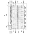
- FIG. 3 is a top view showing a schematic structure of the semiconductor device 3 according to the present embodiment.
- the normally-on transistors Q2 and Q3 of the semiconductor device 3 according to this embodiment are formed by the same wafer process.
- the electrical characteristics of normally-on type transistors Q2 and Q3 can be made comparable.
- the normally-on transistor Q3 is turned on so that the breakdown voltage of the normally-on transistor Q2 does not break down. It is easy to adjust the timing.
- the switching characteristics of the normally-on transistors Q2 and Q3 can be set to the same level, the difference between the turn-on time of the normally-on transistor Q2 and the turn-on time of the normally-on transistor Q3 can be set according to the set value. It becomes easy.
- the wafer process refers to a process of forming elements constituting a semiconductor device on a semiconductor wafer substrate, and the same wafer process refers to a process of the same type performed simultaneously on the same semiconductor wafer. That means.
- normally-on transistors Q2 and Q3 are formed on one semiconductor chip 4 as shown in FIG.
- the normally-on transistors Q2 and Q3 in the semiconductor device 3 according to the present embodiment at a low cost and in a small space.
- the normally-on transistors Q2 and Q3 can be arranged side by side on one semiconductor chip 4, the electrical characteristics of the normally-on transistors Q2 and Q3 can be made more similar.
- the gate electrode of the normally-on transistor Q2 is composed of a lower gate electrode Q2DG and an upper gate electrode Q2UG.
- the rectangular region 5 as viewed from above is a conductive portion between the lower gate electrode Q2DG and the upper gate electrode Q2UG, and is formed between the lower gate electrode Q2DG and the upper gate electrode Q2UG in the thickness direction of the semiconductor chip 4.
- the source electrode of the normally-on transistor Q2 is composed of a lower source electrode Q2DS and an upper source electrode Q2US.
- the rectangular region 6 in a top view is a conductive portion between the lower source electrode Q2DS and the upper source electrode Q2US, and is formed between the lower source electrode Q2DS and the upper source electrode Q2US in the thickness direction of the semiconductor chip 4.
- the drain electrode of the normally-on transistor Q2 is composed of a lower drain electrode Q2DD and an upper drain electrode Q2UD.
- the rectangular region 7 in a top view is a conductive portion between the lower drain electrode Q2DD and the upper drain electrode Q2UD, and is formed between the lower drain electrode Q2DD and the upper drain electrode Q2UD in the thickness direction of the semiconductor chip 4.
- the gate electrode of the normally-on transistor Q3 is composed of a lower gate electrode Q3DG and an upper gate electrode Q3UG.
- the rectangular region 8 when viewed from above is a conductive portion between the lower gate electrode Q3DG and the upper gate electrode Q3UG, and is formed between the lower gate electrode Q3DG and the upper gate electrode Q3UG in the thickness direction of the semiconductor chip 4.
- the source electrode of the normally-on transistor Q3 is composed of a lower source electrode Q3DS and an upper source electrode Q3US.
- the rectangular region 9 as viewed from above is a conductive portion between the lower source electrode Q3DS and the upper source electrode Q3US, and is formed between the lower source electrode Q3DS and the upper source electrode Q3US in the thickness direction of the semiconductor chip 4.
- the drain electrode of the normally-on transistor Q3 is composed of a lower drain electrode Q3DD and an upper drain electrode Q3UD.
- the rectangular region 10 in a top view is a conductive portion between the lower drain electrode Q3DD and the upper drain electrode Q3UD, and is formed between the lower drain electrode Q3DD and the upper drain electrode Q3UD in the thickness direction of the semiconductor chip 4.
- the upper source electrode Q2US of the normally-on transistor Q2 and the upper source electrode Q3US of the normally-on transistor Q3 are formed of the same conductive layer (the same member), and the upper drain electrode Q2UD of the normally-on transistor Q2 and the The upper drain electrode Q3UD of the mullion transistor Q3 is formed by the same conductive layer (same member). That is, all of the electrical connection paths for connecting the normally-on type transistors Q2 and Q3 in parallel are formed on the semiconductor chip 4.
- the semiconductor device described above includes a normally-off type first transistor (Q1), a normally-on type second transistor (Q2), and a normally-on type third transistor (Q3).
- the transistor (Q1) and the second transistor (Q2) are cascode-connected, the third transistor (Q3) is connected in parallel to the second transistor (Q3), and
- the off breakdown voltages of the second transistor (Q2) and the third transistor (Q3) are higher than the off breakdown voltage of the first transistor (Q1), and the turn-on time of the third transistor (Q3) is the second
- This is a configuration (first configuration) that is shorter than the turn-on time of the transistor (Q2).
- the third transistor when an overvoltage is applied to the semiconductor device, the third transistor can be quickly shifted from the off state to the on state, so that the connection point between the first transistor and the second transistor The potential can be lowered before the potential becomes too large. Accordingly, it is possible to prevent the voltage applied to the second transistor from exceeding the off-breakdown voltage and destroying the second transistor.
- the semiconductor device having the first configuration further includes a diode (D1), a power supply terminal (T2), and a ground terminal (T1), and the first transistor (Q1) and the second transistor (Q2).
- the third transistor (Q3) each have a first electrode, a second electrode, and a control electrode, and the power supply terminal (T2) is the first electrode of the second transistor (Q2).
- the second electrode of the first transistor (Q1) is connected to the ground terminal (T1), and the power supply end
- the cathode terminal of the diode (D1) is connected to the (T2) side
- the anode terminal of the diode (D1) is connected to the control electrode side of the third transistor (Q3).
- T2) and the control electrode of the third transistor (Q3) are provided with the diode (D1), and the avalanche voltage of the diode (D1) is the same as the power supply terminal (T2) and the A configuration (second configuration) that is larger than the rated voltage with respect to the ground terminal (T1) and not more than the off breakdown voltage of the third transistor (Q3) may be employed.
- the semiconductor device when the semiconductor device performs a switching operation within the rated voltage range, current can be prevented from flowing between the cathode electrode and the anode electrode of the diode.
- a current flows between the cathode electrode and the anode electrode of the diode, and the third transistor can be automatically shifted from the off state to the on state.
- the potential of the connection point between the first transistor and the second transistor can be lowered before the potential becomes too large. Accordingly, it is possible to prevent the voltage applied to the second transistor from exceeding the off-breakdown voltage and destroying the second transistor.
- the second transistor (Q2) and the third transistor (Q3) are formed by the same wafer process (third configuration). ).
- the electrical characteristics of the second transistor and the third transistor in particular, the off-breakdown voltage between the source electrode and the drain electrode of the second transistor and the third transistor are approximately the same. It is easy to adjust the timing at which the third transistor is turned on so that the breakdown voltage breakdown of the second transistor does not occur.
- the switching characteristics of the second transistor and the third transistor can be made comparable, the difference between the turn-on time of the second transistor and the turn-on time of the third transistor can be set according to the set value. It becomes easy.
- the second transistor (Q2) and the third transistor (Q3) are formed on one semiconductor chip (fourth Configuration).
- the second transistor and the third transistor in the semiconductor device with low cost and a small space.
- the second transistor and the third transistor can be arranged side by side on one semiconductor chip, the electrical characteristics of the second transistor and the third transistor can be made more similar.
- the second transistor (Q2) and the third transistor (Q3) are transistors each using a wide band gap semiconductor (sixth Configuration).
- a transistor using a wide bandgap semiconductor has a high off-breakdown voltage, so that the off-breakdown voltage of the second transistor and the third transistor and thus the breakdown voltage of the semiconductor device can be increased.
- the transistor using the wide band gap semiconductor may be a gallium nitride (GaN) transistor (seventh configuration).
- the gallium nitride (GaN) -based transistor has a high saturation electron velocity and can operate at high speed, so that it is possible to easily increase the breakdown voltage and the high-speed operation of the semiconductor device.
Landscapes
- Semiconductor Integrated Circuits (AREA)
- Junction Field-Effect Transistors (AREA)
- Metal-Oxide And Bipolar Metal-Oxide Semiconductor Integrated Circuits (AREA)
Abstract
Description
本発明の第1実施形態に係る半導体装置について図1を参照して説明する。
本発明の第2実施形態に係る半導体装置について図2を参照して説明する。なお、図2において図1と同一の部品については同一の符号を付してその説明を省略する。
本発明の第3実施形態に係る半導体装置について図3を参照して説明する。本発明の第3実施形態に係る半導体装置は図1に示す第1実施形態に係る半導体装置1と同一の構成である。なお、図3において図1と同一の部品については同一の符号を付してその説明を省略する。
以上、本発明の実施形態につき説明したが、本発明の範囲はこれに限定されるものではなく、発明の主旨を逸脱しない範囲で種々の変更を加えて実施することができる。
2 第2実施形態に係る半導体装置
3 第3実施形態に係る半導体装置
4 半導体チップ
5~10 上面視矩形領域
Q1 ノーマリオフ型トランジスタ
Q2、Q3 ノーマリオン型トランジスタ
Q2DG トランジスタQ2の下部ゲート電極
Q2UG トランジスタQ2の上部ゲート電極
Q2DS トランジスタQ2の下部ソース電極
Q2US トランジスタQ2の上部ソース電極
Q2DD トランジスタQ2の下部ドレイン電極
Q2UD トランジスタQ2の上部ドレイン電極
Q3DG トランジスタQ3の下部ゲート電極
Q3UG トランジスタQ3の上部ゲート電極
Q3DS トランジスタQ3の下部ソース電極
Q3US トランジスタQ3の上部ソース電極
Q3DD トランジスタQ3の下部ドレイン電極
Q3UD トランジスタQ3の上部ドレイン電極
R1、R2 抵抗
T1 グランド端子
T2 電源端子
T3 制御端子
D1 ダイオード
Claims (5)
- ノーマリオフ型の第1のトランジスタと、
ノーマリオン型の第2のトランジスタと、
ノーマリオン型の第3のトランジスタとを備え、
前記第1のトランジスタと前記第2のトランジスタとがカスコード接続されており、
前記第3のトランジスタが前記第2のトランジスタに対して並列に接続されており、
前記第2のトランジスタ及び前記第3のトランジスタの各オフ耐圧が前記第1のトランジスタのオフ耐圧より高く、
前記第3のトランジスタのターンオン時間が前記第2のトランジスタのターンオン時間より短いことを特徴とする半導体装置。 - ダイオードと、電源端子と、グランド端子とをさらに備え、
前記第1のトランジスタ、前記第2のトランジスタ、及び前記第3のトランジスタそれぞれが第1の電極、第2の電極、及び制御電極を有し、
前記電源端子が前記第2のトランジスタの前記第1の電極及び前記第3のトランジスタの前記第1の電極に接続されており、
前記第2のトランジスタの前記第2の電極及び前記第3のトランジスタの前記第2の電極が前記第1のトランジスタの前記第1の電極に接続されており、
前記第1のトランジスタの前記第2の電極が前記グランド端子に接続されており、
前記電源端子側に前記ダイオードのカソード電極が接続され、前記第3のトランジスタの前記制御電極側に前記ダイオードのアノード電極が接続されるように、前記電源端子と、前記第3のトランジスタの前記制御電極との間に、前記ダイオードが設けられており、
前記ダイオードのアバランシェ電圧は、前記電源端子と前記グランド端子との間の定格電圧より大きく、前記第3のトランジスタのオフ耐圧以下であることを特徴とする請求項1に記載の半導体装置。 - 前記第2のトランジスタ及び前記第3のトランジスタが、一つの半導体チップ上に形成されていることを特徴とする請求項1又は請求項2に記載の半導体装置。
- 前記第2のトランジスタ及び前記第3のトランジスタそれぞれがワイドバンドギャップ半導体を用いたトランジスタであることを特徴とする請求項1から請求項3のいずれか一項に記載の半導体装置。
- 前記ワイドバンドギャップ半導体を用いたトランジスタが窒化ガリウム(GaN)系のトランジスタであることを特徴とする請求項4に記載の半導体装置。
Priority Applications (3)
| Application Number | Priority Date | Filing Date | Title |
|---|---|---|---|
| CN201480059057.7A CN105684136A (zh) | 2013-11-26 | 2014-11-05 | 半导体器件 |
| US15/026,546 US20160233209A1 (en) | 2013-11-26 | 2014-11-05 | Semiconductor device |
| JP2015550627A JP6096932B2 (ja) | 2013-11-26 | 2014-11-05 | 半導体装置 |
Applications Claiming Priority (2)
| Application Number | Priority Date | Filing Date | Title |
|---|---|---|---|
| JP2013-244133 | 2013-11-26 | ||
| JP2013244133 | 2013-11-26 |
Publications (1)
| Publication Number | Publication Date |
|---|---|
| WO2015079875A1 true WO2015079875A1 (ja) | 2015-06-04 |
Family
ID=53198823
Family Applications (1)
| Application Number | Title | Priority Date | Filing Date |
|---|---|---|---|
| PCT/JP2014/079310 Ceased WO2015079875A1 (ja) | 2013-11-26 | 2014-11-05 | 半導体装置 |
Country Status (4)
| Country | Link |
|---|---|
| US (1) | US20160233209A1 (ja) |
| JP (1) | JP6096932B2 (ja) |
| CN (1) | CN105684136A (ja) |
| WO (1) | WO2015079875A1 (ja) |
Citations (4)
| Publication number | Priority date | Publication date | Assignee | Title |
|---|---|---|---|---|
| JPH0410317B2 (ja) * | 1984-01-28 | 1992-02-24 | ||
| JPH07263465A (ja) * | 1994-03-24 | 1995-10-13 | Nec Corp | 半導体素子 |
| JP2010530616A (ja) * | 2007-06-13 | 2010-09-09 | ノースロップ グラマン システムズ コーポレーション | 改良された電力用スイッチングトランジスター |
| JP2012235378A (ja) * | 2011-05-06 | 2012-11-29 | Sharp Corp | 半導体装置および電子機器 |
Family Cites Families (7)
| Publication number | Priority date | Publication date | Assignee | Title |
|---|---|---|---|---|
| US5536958A (en) * | 1995-05-02 | 1996-07-16 | Motorola, Inc. | Semiconductor device having high voltage protection capability |
| JP2004266173A (ja) * | 2003-03-04 | 2004-09-24 | Toshiba Corp | 半導体装置 |
| US7202528B2 (en) * | 2004-12-01 | 2007-04-10 | Semisouth Laboratories, Inc. | Normally-off integrated JFET power switches in wide bandgap semiconductors and methods of making |
| US9076853B2 (en) * | 2011-03-18 | 2015-07-07 | International Rectifie Corporation | High voltage rectifier and switching circuits |
| US20120262220A1 (en) * | 2011-04-13 | 2012-10-18 | Semisouth Laboratories, Inc. | Cascode switches including normally-off and normally-on devices and circuits comprising the switches |
| JP5757223B2 (ja) * | 2011-12-02 | 2015-07-29 | 住友電気工業株式会社 | 炭化珪素半導体装置およびその製造方法 |
| KR101922117B1 (ko) * | 2012-08-16 | 2018-11-26 | 삼성전자주식회사 | 트랜지스터를 포함하는 전자소자 및 그 동작방법 |
-
2014
- 2014-11-05 CN CN201480059057.7A patent/CN105684136A/zh active Pending
- 2014-11-05 WO PCT/JP2014/079310 patent/WO2015079875A1/ja not_active Ceased
- 2014-11-05 JP JP2015550627A patent/JP6096932B2/ja not_active Expired - Fee Related
- 2014-11-05 US US15/026,546 patent/US20160233209A1/en not_active Abandoned
Patent Citations (4)
| Publication number | Priority date | Publication date | Assignee | Title |
|---|---|---|---|---|
| JPH0410317B2 (ja) * | 1984-01-28 | 1992-02-24 | ||
| JPH07263465A (ja) * | 1994-03-24 | 1995-10-13 | Nec Corp | 半導体素子 |
| JP2010530616A (ja) * | 2007-06-13 | 2010-09-09 | ノースロップ グラマン システムズ コーポレーション | 改良された電力用スイッチングトランジスター |
| JP2012235378A (ja) * | 2011-05-06 | 2012-11-29 | Sharp Corp | 半導体装置および電子機器 |
Also Published As
| Publication number | Publication date |
|---|---|
| JPWO2015079875A1 (ja) | 2017-03-16 |
| JP6096932B2 (ja) | 2017-03-15 |
| CN105684136A (zh) | 2016-06-15 |
| US20160233209A1 (en) | 2016-08-11 |
Similar Documents
| Publication | Publication Date | Title |
|---|---|---|
| JP6201422B2 (ja) | 半導体装置 | |
| US9653449B2 (en) | Cascoded semiconductor device | |
| US8624662B2 (en) | Semiconductor electronic components and circuits | |
| US9447767B2 (en) | Single chip igniter and internal combustion engine ignition device | |
| JP6203097B2 (ja) | 半導体装置 | |
| EP2549650A1 (en) | Method for driving IGBT | |
| KR20120098667A (ko) | 낮은 emi 회로를 위한 패키지 구성 | |
| JPWO2017010554A1 (ja) | 半導体装置 | |
| JP2020109909A (ja) | 半導体装置及び半導体パッケージ | |
| JP6251387B2 (ja) | 複合型半導体装置 | |
| US9972992B2 (en) | Protection circuit of semiconductor device | |
| JPWO2014034346A1 (ja) | 複合型半導体装置 | |
| US11682719B2 (en) | Vertical insulated gate bipolar transistor (IGBT) with two type control gates | |
| JPWO2016006376A1 (ja) | 半導体装置 | |
| CN107667422A (zh) | 复合型半导体装置 | |
| US8854112B2 (en) | FET drive circuit and FET module | |
| CN205609525U (zh) | 电子设备与集成电路 | |
| US8917117B2 (en) | Composite semiconductor device reducing malfunctions of power semiconductor element switching operation | |
| JP6096932B2 (ja) | 半導体装置 | |
| US20140055192A1 (en) | Saturation current limiting circuit topology for power transistors | |
| CN108735730B (zh) | 电力开关及其半导体装置 | |
| CN102738143B (zh) | 半导体装置、dc-dc 转换器和保护元件 | |
| TW202523143A (zh) | 共源共柵半導體裝置 | |
| JP2007305956A (ja) | 半導体集積回路 | |
| JP2012160495A (ja) | 複合半導体装置 |
Legal Events
| Date | Code | Title | Description |
|---|---|---|---|
| 121 | Ep: the epo has been informed by wipo that ep was designated in this application |
Ref document number: 14866602 Country of ref document: EP Kind code of ref document: A1 |
|
| ENP | Entry into the national phase |
Ref document number: 2015550627 Country of ref document: JP Kind code of ref document: A |
|
| WWE | Wipo information: entry into national phase |
Ref document number: 15026546 Country of ref document: US |
|
| NENP | Non-entry into the national phase |
Ref country code: DE |
|
| 122 | Ep: pct application non-entry in european phase |
Ref document number: 14866602 Country of ref document: EP Kind code of ref document: A1 |