WO2015079707A1 - エポキシ樹脂組成物、半導体封止剤および半導体装置 - Google Patents
エポキシ樹脂組成物、半導体封止剤および半導体装置 Download PDFInfo
- Publication number
- WO2015079707A1 WO2015079707A1 PCT/JP2014/005966 JP2014005966W WO2015079707A1 WO 2015079707 A1 WO2015079707 A1 WO 2015079707A1 JP 2014005966 W JP2014005966 W JP 2014005966W WO 2015079707 A1 WO2015079707 A1 WO 2015079707A1
- Authority
- WO
- WIPO (PCT)
- Prior art keywords
- epoxy resin
- component
- resin composition
- bleed
- average particle
- Prior art date
- Legal status (The legal status is an assumption and is not a legal conclusion. Google has not performed a legal analysis and makes no representation as to the accuracy of the status listed.)
- Ceased
Links
Images


Classifications
-
- H—ELECTRICITY
- H10—SEMICONDUCTOR DEVICES; ELECTRIC SOLID-STATE DEVICES NOT OTHERWISE PROVIDED FOR
- H10W—GENERIC PACKAGES, INTERCONNECTIONS, CONNECTORS OR OTHER CONSTRUCTIONAL DETAILS OF DEVICES COVERED BY CLASS H10
- H10W74/00—Encapsulations, e.g. protective coatings
- H10W74/40—Encapsulations, e.g. protective coatings characterised by their materials
- H10W74/47—Encapsulations, e.g. protective coatings characterised by their materials comprising organic materials, e.g. plastics or resins
- H10W74/473—Encapsulations, e.g. protective coatings characterised by their materials comprising organic materials, e.g. plastics or resins containing a filler
-
- C—CHEMISTRY; METALLURGY
- C08—ORGANIC MACROMOLECULAR COMPOUNDS; THEIR PREPARATION OR CHEMICAL WORKING-UP; COMPOSITIONS BASED THEREON
- C08G—MACROMOLECULAR COMPOUNDS OBTAINED OTHERWISE THAN BY REACTIONS ONLY INVOLVING UNSATURATED CARBON-TO-CARBON BONDS
- C08G59/00—Polycondensates containing more than one epoxy group per molecule; Macromolecules obtained by polymerising compounds containing more than one epoxy group per molecule using curing agents or catalysts which react with the epoxy groups
- C08G59/18—Macromolecules obtained by polymerising compounds containing more than one epoxy group per molecule using curing agents or catalysts which react with the epoxy groups ; e.g. general methods of curing
- C08G59/20—Macromolecules obtained by polymerising compounds containing more than one epoxy group per molecule using curing agents or catalysts which react with the epoxy groups ; e.g. general methods of curing characterised by the epoxy compounds used
- C08G59/22—Di-epoxy compounds
- C08G59/24—Di-epoxy compounds carbocyclic
- C08G59/245—Di-epoxy compounds carbocyclic aromatic
-
- C—CHEMISTRY; METALLURGY
- C08—ORGANIC MACROMOLECULAR COMPOUNDS; THEIR PREPARATION OR CHEMICAL WORKING-UP; COMPOSITIONS BASED THEREON
- C08G—MACROMOLECULAR COMPOUNDS OBTAINED OTHERWISE THAN BY REACTIONS ONLY INVOLVING UNSATURATED CARBON-TO-CARBON BONDS
- C08G59/00—Polycondensates containing more than one epoxy group per molecule; Macromolecules obtained by polymerising compounds containing more than one epoxy group per molecule using curing agents or catalysts which react with the epoxy groups
- C08G59/18—Macromolecules obtained by polymerising compounds containing more than one epoxy group per molecule using curing agents or catalysts which react with the epoxy groups ; e.g. general methods of curing
- C08G59/40—Macromolecules obtained by polymerising compounds containing more than one epoxy group per molecule using curing agents or catalysts which react with the epoxy groups ; e.g. general methods of curing characterised by the curing agents used
- C08G59/50—Amines
-
- C—CHEMISTRY; METALLURGY
- C08—ORGANIC MACROMOLECULAR COMPOUNDS; THEIR PREPARATION OR CHEMICAL WORKING-UP; COMPOSITIONS BASED THEREON
- C08J—WORKING-UP; GENERAL PROCESSES OF COMPOUNDING; AFTER-TREATMENT NOT COVERED BY SUBCLASSES C08B, C08C, C08F, C08G or C08H
- C08J3/00—Processes of treating or compounding macromolecular substances
- C08J3/20—Compounding polymers with additives, e.g. colouring
- C08J3/22—Compounding polymers with additives, e.g. colouring using masterbatch techniques
-
- C—CHEMISTRY; METALLURGY
- C08—ORGANIC MACROMOLECULAR COMPOUNDS; THEIR PREPARATION OR CHEMICAL WORKING-UP; COMPOSITIONS BASED THEREON
- C08K—Use of inorganic or non-macromolecular organic substances as compounding ingredients
- C08K3/00—Use of inorganic substances as compounding ingredients
- C08K3/34—Silicon-containing compounds
- C08K3/36—Silica
-
- C—CHEMISTRY; METALLURGY
- C08—ORGANIC MACROMOLECULAR COMPOUNDS; THEIR PREPARATION OR CHEMICAL WORKING-UP; COMPOSITIONS BASED THEREON
- C08K—Use of inorganic or non-macromolecular organic substances as compounding ingredients
- C08K9/00—Use of pretreated ingredients
- C08K9/04—Ingredients treated with organic substances
- C08K9/06—Ingredients treated with organic substances with silicon-containing compounds
-
- C—CHEMISTRY; METALLURGY
- C08—ORGANIC MACROMOLECULAR COMPOUNDS; THEIR PREPARATION OR CHEMICAL WORKING-UP; COMPOSITIONS BASED THEREON
- C08L—COMPOSITIONS OF MACROMOLECULAR COMPOUNDS
- C08L63/00—Compositions of epoxy resins; Compositions of derivatives of epoxy resins
-
- H—ELECTRICITY
- H10—SEMICONDUCTOR DEVICES; ELECTRIC SOLID-STATE DEVICES NOT OTHERWISE PROVIDED FOR
- H10H—INORGANIC LIGHT-EMITTING SEMICONDUCTOR DEVICES HAVING POTENTIAL BARRIERS
- H10H20/00—Individual inorganic light-emitting semiconductor devices having potential barriers, e.g. light-emitting diodes [LED]
- H10H20/80—Constructional details
- H10H20/85—Packages
- H10H20/852—Encapsulations
- H10H20/854—Encapsulations characterised by their material, e.g. epoxy or silicone resins
-
- H—ELECTRICITY
- H10—SEMICONDUCTOR DEVICES; ELECTRIC SOLID-STATE DEVICES NOT OTHERWISE PROVIDED FOR
- H10W—GENERIC PACKAGES, INTERCONNECTIONS, CONNECTORS OR OTHER CONSTRUCTIONAL DETAILS OF DEVICES COVERED BY CLASS H10
- H10W72/00—Interconnections or connectors in packages
- H10W72/30—Die-attach connectors
-
- C—CHEMISTRY; METALLURGY
- C08—ORGANIC MACROMOLECULAR COMPOUNDS; THEIR PREPARATION OR CHEMICAL WORKING-UP; COMPOSITIONS BASED THEREON
- C08K—Use of inorganic or non-macromolecular organic substances as compounding ingredients
- C08K2201/00—Specific properties of additives
- C08K2201/002—Physical properties
- C08K2201/005—Additives being defined by their particle size in general
-
- C—CHEMISTRY; METALLURGY
- C08—ORGANIC MACROMOLECULAR COMPOUNDS; THEIR PREPARATION OR CHEMICAL WORKING-UP; COMPOSITIONS BASED THEREON
- C08K—Use of inorganic or non-macromolecular organic substances as compounding ingredients
- C08K2201/00—Specific properties of additives
- C08K2201/014—Additives containing two or more different additives of the same subgroup in C08K
-
- H—ELECTRICITY
- H10—SEMICONDUCTOR DEVICES; ELECTRIC SOLID-STATE DEVICES NOT OTHERWISE PROVIDED FOR
- H10W—GENERIC PACKAGES, INTERCONNECTIONS, CONNECTORS OR OTHER CONSTRUCTIONAL DETAILS OF DEVICES COVERED BY CLASS H10
- H10W72/00—Interconnections or connectors in packages
- H10W72/071—Connecting or disconnecting
- H10W72/073—Connecting or disconnecting of die-attach connectors
-
- H—ELECTRICITY
- H10—SEMICONDUCTOR DEVICES; ELECTRIC SOLID-STATE DEVICES NOT OTHERWISE PROVIDED FOR
- H10W—GENERIC PACKAGES, INTERCONNECTIONS, CONNECTORS OR OTHER CONSTRUCTIONAL DETAILS OF DEVICES COVERED BY CLASS H10
- H10W72/00—Interconnections or connectors in packages
- H10W72/071—Connecting or disconnecting
- H10W72/073—Connecting or disconnecting of die-attach connectors
- H10W72/07331—Connecting techniques
- H10W72/07337—Connecting techniques using a polymer adhesive, e.g. an adhesive based on silicone or epoxy
-
- H—ELECTRICITY
- H10—SEMICONDUCTOR DEVICES; ELECTRIC SOLID-STATE DEVICES NOT OTHERWISE PROVIDED FOR
- H10W—GENERIC PACKAGES, INTERCONNECTIONS, CONNECTORS OR OTHER CONSTRUCTIONAL DETAILS OF DEVICES COVERED BY CLASS H10
- H10W72/00—Interconnections or connectors in packages
- H10W72/071—Connecting or disconnecting
- H10W72/073—Connecting or disconnecting of die-attach connectors
- H10W72/07331—Connecting techniques
- H10W72/07337—Connecting techniques using a polymer adhesive, e.g. an adhesive based on silicone or epoxy
- H10W72/07338—Connecting techniques using a polymer adhesive, e.g. an adhesive based on silicone or epoxy hardening the adhesive by curing, e.g. thermosetting
-
- H—ELECTRICITY
- H10—SEMICONDUCTOR DEVICES; ELECTRIC SOLID-STATE DEVICES NOT OTHERWISE PROVIDED FOR
- H10W—GENERIC PACKAGES, INTERCONNECTIONS, CONNECTORS OR OTHER CONSTRUCTIONAL DETAILS OF DEVICES COVERED BY CLASS H10
- H10W72/00—Interconnections or connectors in packages
- H10W72/20—Bump connectors, e.g. solder bumps or copper pillars; Dummy bumps; Thermal bumps
- H10W72/251—Materials
- H10W72/252—Materials comprising solid metals or solid metalloids, e.g. PbSn, Ag or Cu
-
- H—ELECTRICITY
- H10—SEMICONDUCTOR DEVICES; ELECTRIC SOLID-STATE DEVICES NOT OTHERWISE PROVIDED FOR
- H10W—GENERIC PACKAGES, INTERCONNECTIONS, CONNECTORS OR OTHER CONSTRUCTIONAL DETAILS OF DEVICES COVERED BY CLASS H10
- H10W72/00—Interconnections or connectors in packages
- H10W72/30—Die-attach connectors
- H10W72/321—Structures or relative sizes of die-attach connectors
- H10W72/325—Die-attach connectors having a filler embedded in a matrix
-
- H—ELECTRICITY
- H10—SEMICONDUCTOR DEVICES; ELECTRIC SOLID-STATE DEVICES NOT OTHERWISE PROVIDED FOR
- H10W—GENERIC PACKAGES, INTERCONNECTIONS, CONNECTORS OR OTHER CONSTRUCTIONAL DETAILS OF DEVICES COVERED BY CLASS H10
- H10W72/00—Interconnections or connectors in packages
- H10W72/30—Die-attach connectors
- H10W72/351—Materials of die-attach connectors
- H10W72/353—Materials of die-attach connectors not comprising solid metals or solid metalloids, e.g. ceramics
-
- H—ELECTRICITY
- H10—SEMICONDUCTOR DEVICES; ELECTRIC SOLID-STATE DEVICES NOT OTHERWISE PROVIDED FOR
- H10W—GENERIC PACKAGES, INTERCONNECTIONS, CONNECTORS OR OTHER CONSTRUCTIONAL DETAILS OF DEVICES COVERED BY CLASS H10
- H10W72/00—Interconnections or connectors in packages
- H10W72/30—Die-attach connectors
- H10W72/351—Materials of die-attach connectors
- H10W72/353—Materials of die-attach connectors not comprising solid metals or solid metalloids, e.g. ceramics
- H10W72/354—Materials of die-attach connectors not comprising solid metals or solid metalloids, e.g. ceramics comprising polymers
-
- H—ELECTRICITY
- H10—SEMICONDUCTOR DEVICES; ELECTRIC SOLID-STATE DEVICES NOT OTHERWISE PROVIDED FOR
- H10W—GENERIC PACKAGES, INTERCONNECTIONS, CONNECTORS OR OTHER CONSTRUCTIONAL DETAILS OF DEVICES COVERED BY CLASS H10
- H10W74/00—Encapsulations, e.g. protective coatings
- H10W74/10—Encapsulations, e.g. protective coatings characterised by their shape or disposition
- H10W74/15—Encapsulations, e.g. protective coatings characterised by their shape or disposition on active surfaces of flip-chip devices, e.g. underfills
-
- H—ELECTRICITY
- H10—SEMICONDUCTOR DEVICES; ELECTRIC SOLID-STATE DEVICES NOT OTHERWISE PROVIDED FOR
- H10W—GENERIC PACKAGES, INTERCONNECTIONS, CONNECTORS OR OTHER CONSTRUCTIONAL DETAILS OF DEVICES COVERED BY CLASS H10
- H10W90/00—Package configurations
- H10W90/701—Package configurations characterised by the relative positions of pads or connectors relative to package parts
- H10W90/721—Package configurations characterised by the relative positions of pads or connectors relative to package parts of bump connectors
- H10W90/724—Package configurations characterised by the relative positions of pads or connectors relative to package parts of bump connectors between a chip and a stacked insulating package substrate, interposer or RDL
-
- H—ELECTRICITY
- H10—SEMICONDUCTOR DEVICES; ELECTRIC SOLID-STATE DEVICES NOT OTHERWISE PROVIDED FOR
- H10W—GENERIC PACKAGES, INTERCONNECTIONS, CONNECTORS OR OTHER CONSTRUCTIONAL DETAILS OF DEVICES COVERED BY CLASS H10
- H10W90/00—Package configurations
- H10W90/701—Package configurations characterised by the relative positions of pads or connectors relative to package parts
- H10W90/731—Package configurations characterised by the relative positions of pads or connectors relative to package parts of die-attach connectors
- H10W90/734—Package configurations characterised by the relative positions of pads or connectors relative to package parts of die-attach connectors between a chip and a stacked insulating package substrate, interposer or RDL
Definitions
- the present invention relates to an epoxy resin composition, a semiconductor encapsulant, and a semiconductor device.
- Flip chip mounting is a technique for electrically connecting a semiconductor element and a substrate using bumps (solder balls).
- a resin composition is filled between the semiconductor element and the substrate.
- a plasma treatment of the substrate is performed before applying the sealing agent in order to improve the wettability between the substrate surface and the sealing agent.
- a sealing agent is applied to a substrate that has been subjected to plasma treatment, a phenomenon called “bleed” in which a liquid component derived from the sealing agent oozes out around the semiconductor element may occur.
- the bleed may cause not only a poor appearance but also a poor conductivity of the electrode.
- Patent document 1 is disclosing the liquid sealing resin composition containing the liquid silicone compound which has a carboxyl group or an amino group.
- Patent document 2 is disclosing the insulating paste containing a silicone rubber fine powder.
- Patent Documents 3 and 4 disclose a side fill material containing an alkyl methacrylate copolymer, an inorganic filler surface-treated with a non-reactive organosilicon compound, and a modified silicone resin.
- the present invention provides an epoxy resin composition having a simpler composition and excellent in suppressing bleeding.
- the present invention includes (A) an epoxy resin, (B) a curing agent, (C) 0.1 to 10% by mass of silica filler having an average particle size of 10 to 100 nm, and (D) 40 to 75% by mass.
- An epoxy resin composition comprising a silica filler having an average particle size of 0.3 ⁇ m to 5 ⁇ m and a total of 40.1 to 77% by mass of the component (C) and the component (D) To do.
- At least one of the component (C) and the component (D) may be surface-treated with a silane coupling agent.
- the component (D) may be surface-treated with an aminosilane represented by the formula (1).
- the equivalent ratio of the component (A) and the component (B) may be 0.5 to 1.8.
- the component (B) may be an amine curing agent.
- the component (A) may include at least one of bisphenol F type epoxy resin, bisphenol A type epoxy resin, naphthalene type epoxy resin, and aminophenol type epoxy resin.
- the bleed generated in the bleed test of the cured product of the epoxy resin composition may be 300 ⁇ m or more and less than 1900 ⁇ m.
- the epoxy resin composition may be produced by mixing the component (C) with at least a part of the component (A) to produce a master batch, and mixing the other components with the master batch.
- the present invention also provides a semiconductor encapsulant using the above epoxy resin composition.
- the present invention provides a semiconductor device using the above semiconductor encapsulant.
- bleeding can be suppressed by using an epoxy resin composition having a simpler composition.
- FIG. 1A is a diagram illustrating bleed.
- FIG. 1B is a diagram illustrating bleed.
- FIGS. 1A and 1B are diagrams for explaining a bleed generated in mounting a semiconductor element.
- FIG. 1A shows a view from the top surface of the chip.
- FIG. 1B shows an AA cross section of FIG. 1A.
- an underfill agent UF sealing agent
- the bleed is generated on the outside. In addition to appearing discolored in appearance, the bleed may affect the characteristics and reliability of the device.
- the inventors of the present application observed a bleed portion and a non-bleed portion on a sample prepared by mounting a semiconductor element on a substrate with a scanning electron microscope (SEM).
- SEM scanning electron microscope
- a composition containing an epoxy resin, a curing agent, a silica filler, and other additives was used as a sealant.
- the inventors analyzed the bleed portion and the non-bleed portion by XPS (X-ray Photoelectron tro Spectroscopy). As a result, there was no difference in components between the bleed part and the non-bleed part except for the silica filler.
- the bleed is formed when components other than the silica filler (for example, epoxy resin and curing agent) out of the fillet ooze out of the fillet.
- a sample that was plasma-treated before application of the sealant was compared with a sample that was not plasma-treated. As a result, bleeding occurred in the sample subjected to the plasma treatment. However, bleed did not occur in the sample that was not plasma-treated.
- the inventors of the present application considered that bleed occurs when the liquid resin component other than the filler exudes into the fine irregularities on the surface of the substrate formed by plasma treatment due to capillary action. Therefore, in order to suppress the seepage of the liquid resin component due to the capillary phenomenon, the inventors have come up with the idea of using a small-diameter filler to stop the seepage of the liquid resin component.
- the epoxy resin composition of the present invention comprises (A) an epoxy resin, (B) a curing agent, (C) a small diameter silica filler, and (D) a large diameter silica filler.
- component (A) examples include bisphenol A type epoxy resin, bisphenol F type epoxy resin, naphthalene type epoxy resin, aminophenol type epoxy resin, phenol novolac type epoxy resin, alicyclic epoxy resin, siloxane type epoxy resin, biphenyl type Examples include epoxy resins, glycidyl ester type epoxy resins, glycidyl amine type epoxy resins, and hydantoin type epoxy resins. Among these, bisphenol F type epoxy resin, bisphenol A type epoxy resin, naphthalene type epoxy resin, and aminophenol type epoxy resin are preferable. In the epoxy resin composition, the compounds exemplified here may be used alone or in combination of two or more.
- the component (B) examples include amine-based curing agents, acid anhydride-based curing agents, and phenol-based curing agents. From the viewpoint of reflow resistance and moisture resistance of the encapsulating liquid resin composition, an amine curing agent is preferably used.
- the equivalent ratio of the component (A) and the component (B) is preferably 0.5 to 1.8.
- Examples of the component (C) and the component (D) include amorphous silica, crystalline silica, fused silica, ground silica, and nano silica.
- Amorphous silica is preferably used from the viewpoint of the thermal expansion coefficient of the cured resin composition.
- Examples of the shapes of the component (C) and the component (D) include a spherical shape, a flake shape, and an indefinite shape. From the viewpoint of fluidity of the resin composition, a spherical one is preferably used.
- the average particle diameter of the component (C) and the component (D) is measured by, for example, a dynamic light scattering nanotrack particle size analyzer. In addition, the average particle diameter here is D50 (median diameter).
- At least one of the component (C) and the component (D) may be surface-treated with a silane coupling agent.
- a silane coupling agent used for the surface treatment include various silane coupling agents such as epoxy, methacrylic, amino, vinyl, glycidoxy, and mercapto. Among these, it is preferable to use aminosilane of following Formula (1) for the surface treatment of (D) component.
- the epoxy resin composition includes an ion trap agent, a pigment, a dye, an antifoaming agent, a stress relaxation agent, a pH adjuster, an accelerator, An additive such as a surfactant and a coupling agent may be included.
- the epoxy resin composition is produced, for example, by stirring, melting, mixing, or dispersing the components (A) to (D) and other additives simultaneously or separately with heat treatment as necessary.
- the These methods such as mixing, stirring, and dispersion are not particularly limited.
- a laika machine equipped with a stirring and heating device, a three-roll mill, a ball mill, a planetary mixer, a bead mill, or the like can be used. Moreover, you may use combining these apparatuses. Here, you may prepare a masterbatch by mixing (A) component and (C) component.
- An epoxy resin composition can be produced by mixing the obtained master batch with other components.
- the epoxy resin composition preferably has a bleed generated in a bleed test described later having a value of 300 or more and less than 1900.
- the epoxy resin composition can be used as an encapsulant (underfill agent) for flip chip mounting or BGA (Ball Grid Array) / CSP (Chip Size Package) mounting of electronic devices such as semiconductor elements.
- This epoxy resin composition may be used as an adhesive when the electronic device is bonded to a substrate or a package.
- a semiconductor element and a substrate are first joined.
- a sealing agent is injected into the gap between the semiconductor element and the substrate.
- a sealant is applied along the outer periphery of the semiconductor element.
- the sealant spreads in the gap by capillary action. Accordingly, the sealant is preferably liquid at the temperature at which this process is performed.
- the injected sealing agent is thermally cured by heating (for example, 80 to 165 ° C.).
- Example 3-1 Preparation of Epoxy Resin Composition
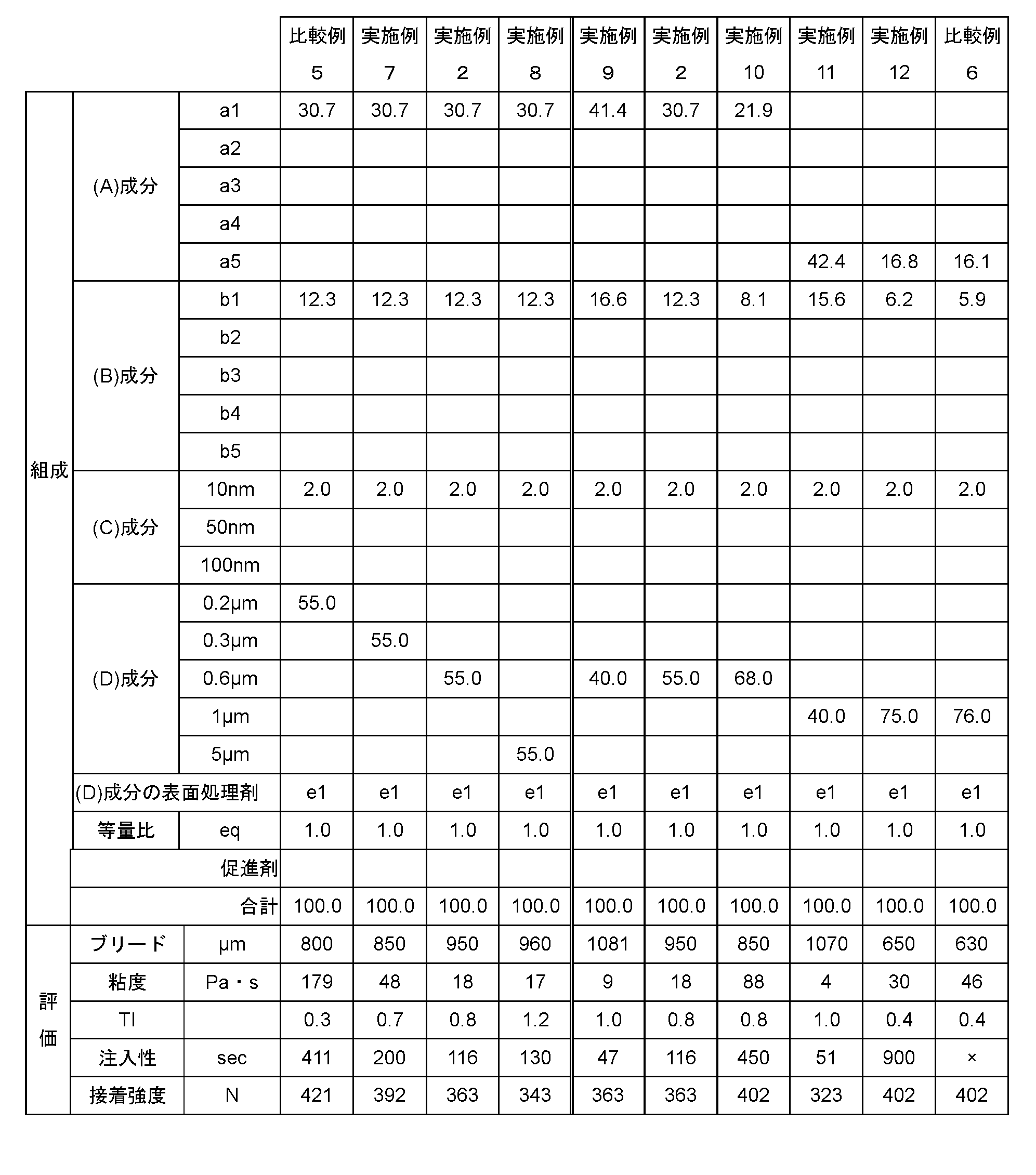
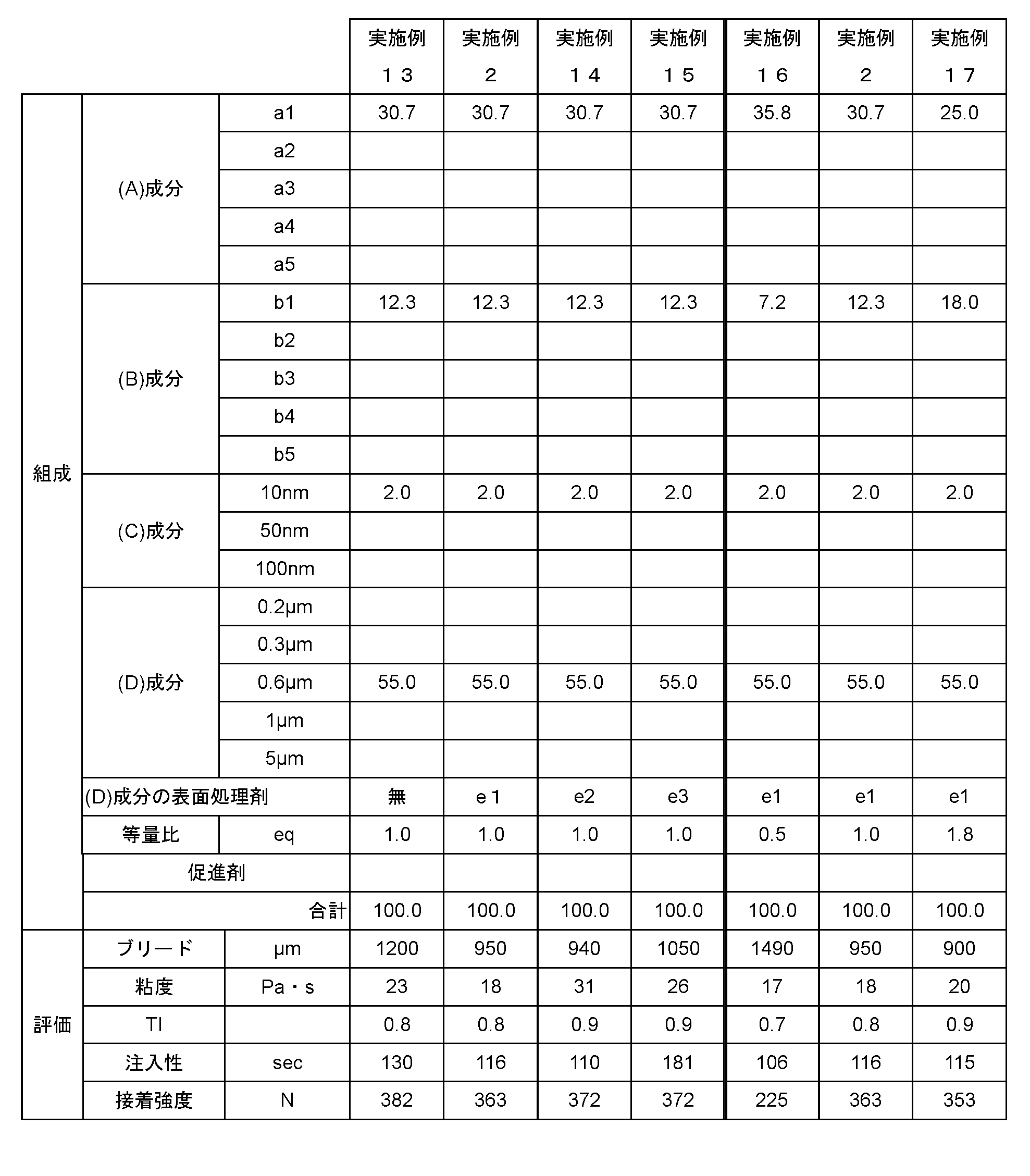
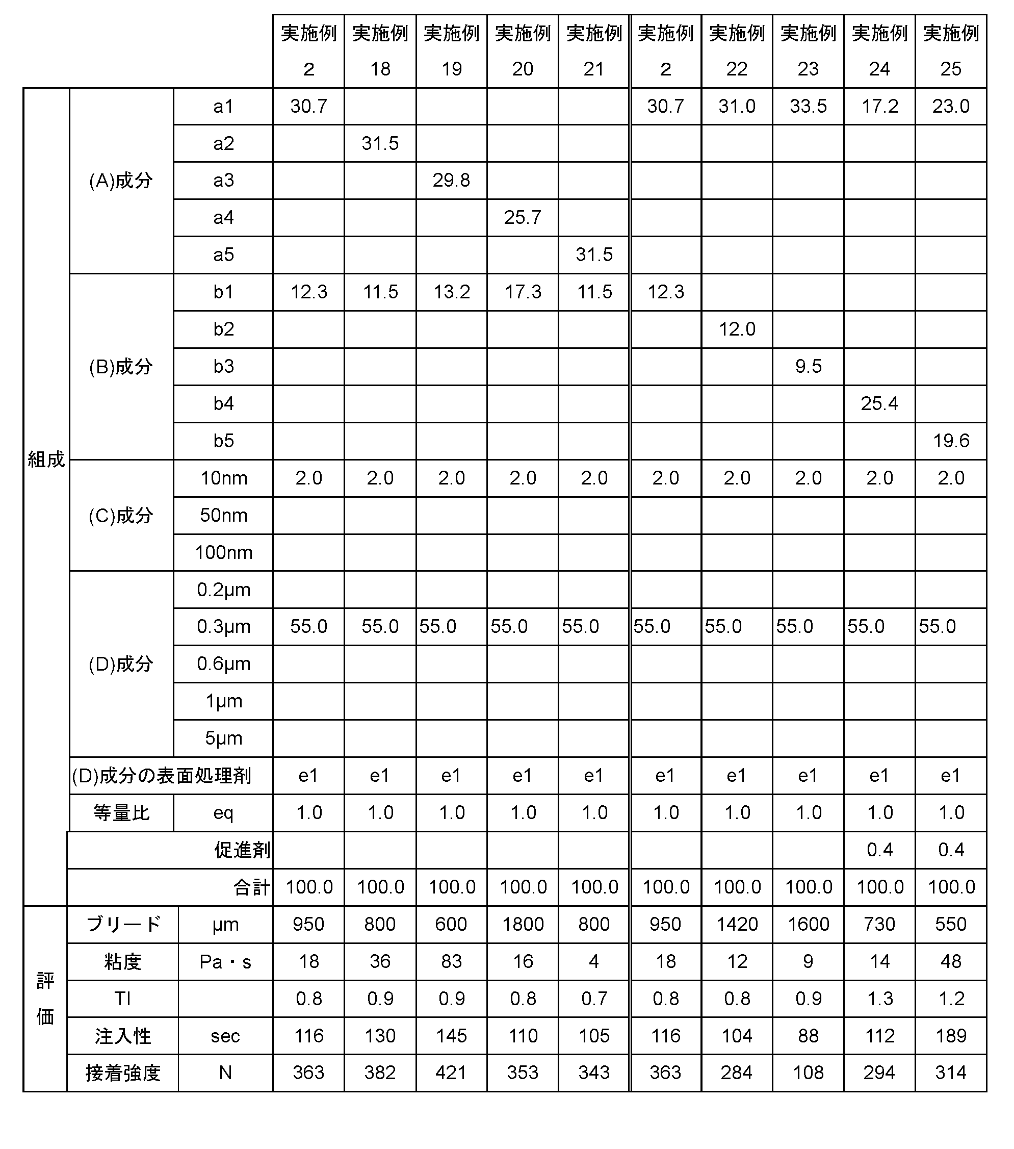
- Tables 1 to 4 show the compositions of the epoxy resin compositions used as sealants in Examples 1 to 25 and Comparative Examples 1 to 6. These tables also show the evaluation results of the epoxy resin composition as a sealant, which will be described later.
- the composition of the epoxy resin composition is expressed in mass%, excluding the equivalence ratio.
- any one of the epoxy resins a1 to a5 was used.
- the epoxy resin a1 YDF8170 manufactured by Nippon Steel & Sumikin Chemical Co., Ltd. was used.
- the epoxy resin a2, 850CRP manufactured by DIC Corporation was used.
- the epoxy resin a3, HP-4032D manufactured by DIC Corporation was used.
- the epoxy resin a4, jer630 manufactured by Mitsubishi Chemical Corporation was used.
- the epoxy resin a5 ZX1658GS manufactured by Toto Kasei Co., Ltd. was used.
- any one of the curing agents b1 to b5 was used.
- Curing agents b1 to b3 are amine curing agents.
- the curing agent b4 is an acid anhydride curing agent.
- the curing agent b5 is a phenolic curing agent.
- As the curing agent b1 Kayahard AA manufactured by Nippon Kayaku Co., Ltd. was used. EH105L manufactured by Adeka Corporation was used as the curing agent b2.
- ETHACURE 100 manufactured by Albermarle was used.
- As the curing agent b4, YH307 manufactured by Mitsubishi Chemical Corporation was used.
- MEH-8005 manufactured by Meiwa Kasei Co., Ltd. was used.
- any of YA010C (average particle size: 10 nm), YA050C (average particle size: 50 nm), and YC100C (average particle size: 100 nm) manufactured by Admatechs Co., Ltd. is used. It was.
- the average particle diameter is a median diameter (D50).
- the average particle diameter is a value measured by a field emission scanning electron microscope (FE-SEM).
- 0.2 ⁇ m high average particle size: 0.2 ⁇ m
- SE-1050 average particle size: 0.3 ⁇ m
- Admatechs SE -300 (average particle size: 0.6 ⁇ m)
- SE-4050 average particle size: 1 ⁇ m
- FB-5D average particle size: 5 ⁇ m
- the average particle diameter is a median diameter (D50).
- the average particle diameter is a value measured by a laser diffraction / scattering particle size distribution meter.
- any of the surface treatment agents e1 to e3 was used as the surface treatment agent for the component (D).
- As the surface treating agent e1 KBM403 (3-glycidoxypropyltrimethoxysilane) manufactured by Shin-Etsu Chemical Co., Ltd. was used.
- As the surface treatment agent e2 KBM503 (3-methacryloxypropyltrimethoxysilane) manufactured by Shin-Etsu Chemical Co., Ltd. was used.
- KBE9103 3-triethoxysilyl-N- (1,3-dimethyl-butylidene) propylamine
- the viscosity of the epoxy resin composition was measured at a TI (thixotropic index) value of 5 rpm and 50 rpm. A value obtained by dividing the measured viscosity value at 5 rpm by the viscosity value at 50 rpm was defined as a TI value.
- Comparative Example 1 shows an example using an epoxy resin composition to which component (C) is not added.
- the bleed length of the sample was 2000 ⁇ m.
- Examples 1 to 4 and Comparative Examples 1 to 3 show examples in which the content of the component (C) is changed.
- the bleed length becomes shorter.
- the bleed length is less than 1900 ⁇ m. That is, when the content of the component (C) is 0.1% by mass or more, bleeding is suppressed.
- the content of the component (C) when the content of the component (C) was 11% by mass, the viscosity was 121 Pa ⁇ s. Therefore, it is preferable that content of (C) component is 10 mass% or less from a viewpoint of the moderate viscosity as a sealing agent. Therefore, the content of the component (C) with respect to the total amount of the epoxy resin composition is preferably 0.1 to 10% by mass.
- Examples 2, 5, and 6 and Comparative Example 4 show examples in which the average particle diameter of the component (C) is changed.
- component (D) having an average particle size of 0.2 ⁇ m that is, 200 nm
- the bleed length is reduced.
- the average particle size of the component (C) is 200 nm or more, defects occur in the bleed test.
- bleeding was suppressed when the average particle size was in the range of 10 to 100 nm. Since Example 2 is frequently referred to below, Example 2 is repeatedly described in Tables 1 to 4 for convenience of explanation.
- Comparative Example 5 and Examples 2, 7, and 8 show examples in which the average particle diameter of the component (D) is changed. As the average particle size of component (D) increases, the viscosity improves. When the average particle size of component (D) was 0.2 ⁇ m or less, the viscosity was 179 Pa ⁇ s. From the viewpoint of moderate viscosity as a sealant, the average particle size of the component (D) is preferably 0.3 ⁇ m or more.
- Examples 2 and 9 to 12 and Comparative Example 6 show examples in which the content of the component (D) is changed.
- the content of the component (D) is reduced, the injectability is improved.
- the content of component (D) is in the range of 40 to 75% by mass, good injectability was exhibited and bleeding was also suppressed.
- the content of the component (D) is preferably 75% by mass or less from the viewpoint of moderate injectability as a sealant.
- the component (C) and the component (D) are preferably contained in a total amount of 40.1 to 77% by mass with respect to the total amount of the resin composition.
- Examples 2 and 13 to 15 show examples in which the surface treatment agent of the component (D) is changed. Bleed is further suppressed by performing the surface treatment. Moreover, viscosity and injectability were improved by using the surface treating agent e1.
- Examples 2, 16, and 17 show examples in which the equivalent ratio between the epoxy resin (component (A)) and the curing agent (component (B)) is changed.
- the equivalence ratio is in the range of 0.5 to 1.8, bleeding is suppressed.
- Examples 2 and 18 to 21 show examples in which the component (A) is changed.
- any of the epoxy resins a1 to a5 is used, bleeding is suppressed.
- Examples 2 and 22 to 25 show examples in which the component (B) is changed. Even if any of the curing agents b1 to b5 is used, bleeding is suppressed.
- the epoxy resin composition according to the present invention may be the following first to eighth epoxy resin compositions.
- the first epoxy resin composition comprises (A) an epoxy resin, (B) a curing agent, (C) a silica filler having an average particle diameter of 10 to 100 nm of 0.1 to 10% by mass, and (D) 40 to 75% by mass of silica filler having an average particle diameter of 0.3 ⁇ m to 5 ⁇ m, and the component (C) and the component (D) are contained in a total amount of 40.1 to 77% by mass.
- An epoxy resin composition is an epoxy resin, (B) a curing agent, (C) a silica filler having an average particle diameter of 10 to 100 nm of 0.1 to 10% by mass, and (D) 40 to 75% by mass of silica filler having an average particle diameter of 0.3 ⁇ m to 5 ⁇ m, and the component (C) and the component (D) are contained in a total amount of 40.1 to 77% by mass.
- the second epoxy resin composition is the first epoxy resin composition, wherein at least one of the component (C) and the component (D) is surface-treated with a silane coupling agent. is there.
- the third epoxy resin composition is the first or second epoxy resin composition, wherein the component (D) is surface-treated with an aminosilane having a structure of the formula (1).
- the equivalent ratio of the component (A) to the component (B) is 0.5 to 1.8. It is an epoxy resin composition of description.
- the fifth epoxy resin composition is the epoxy resin composition according to any one of the first to fourth aspects, wherein the component (B) is an amine curing agent.
- the sixth epoxy resin composition is characterized in that the component (A) contains at least one of bisphenol F type epoxy resin, bisphenol A type epoxy resin, naphthalene type epoxy resin, and aminophenol type epoxy resin.
- the epoxy resin composition according to any one of 1 to 5 above.
- the seventh epoxy resin composition is the epoxy resin composition according to any one of the first to sixth aspects, wherein a generated bleed is 300 ⁇ m or more and less than 1900 ⁇ m in a bleed test of a cured product.
- the eighth epoxy resin composition is manufactured by mixing the component (C) with at least a part of the component (A) to produce a master batch, and mixing the other components with the master batch.
- the epoxy resin composition according to any one of claims 1 to 7, wherein
- the semiconductor encapsulant according to the present invention may be a semiconductor encapsulant using any one of the above epoxy resin compositions 1 to 8.
- the semiconductor device according to the present invention may be a semiconductor device using the ninth semiconductor encapsulant.
Landscapes
- Chemical & Material Sciences (AREA)
- Health & Medical Sciences (AREA)
- Chemical Kinetics & Catalysis (AREA)
- Medicinal Chemistry (AREA)
- Polymers & Plastics (AREA)
- Organic Chemistry (AREA)
- Structures Or Materials For Encapsulating Or Coating Semiconductor Devices Or Solid State Devices (AREA)
- Epoxy Resins (AREA)
- Compositions Of Macromolecular Compounds (AREA)
- Wire Bonding (AREA)
- Processes Of Treating Macromolecular Substances (AREA)
Abstract
Description
本願は、2013年11月29日に出願された日本特許出願「特願2013-247267」に基づく優先権を主張すると共に、参照によりその内容を組み込む。
特許文献3および4は、メタクリル酸アルキル共重合体、非反応性有機ケイ素化合物で表面処理された無機充填剤、および変性シリコーン樹脂を含有するサイドフィル材を開示している。

図1AおよびBは、半導体素子の実装において発生したブリードを説明する図である。ここでは、基板1の上に半導体素子2をアンダーフィル剤により接合した例を示している。図1Aはチップ上面から見た図を示している。図1Bは図1AのA-A断面を示している。半導体素子2の周辺に、アンダーフィル剤UF(封止剤)が盛られている部分(以下「フィレット」という)がある。その外側に発生しているのがブリードである。ブリードは外観上、変色して見えるだけでなく、装置の特性および信頼性に影響を与える場合がある。
本発明のエポキシ樹脂組成物は、(A)エポキシ樹脂と、(B)硬化剤と、(C)小径シリカフィラーと、(D)大径シリカフィラーとを含む。

3-1.エポキシ樹脂組成物の調整
表1~4は、実施例1~25および比較例1~6で、封止剤として用いられたエポキシ樹脂組成物の組成を示す。また、これらの表は、後述する、封止剤としてのエポキシ樹脂組成物の評価結果をも示す。表1~4において、エポキシ樹脂組成物の組成は、等量比を除いて、質量%で表されている。
実施例1~25および比較例1~6で用いられたエポキシ樹脂組成物について、以下の評価を行った。
試料としてソルダーレジスト(PSR4000 AUS703)付きの有機基板(FR-4基板)を用いた。まず試料を150℃で1時間、乾燥させた。次にこの試料をプラズマ処理した。プラズマ処理の条件は以下のとおりである。
ガス種:Ar
ガス流量:21sccm
供給電力:400W
処理時間:300sec
ブルックフィールド回転粘度計を用いて、50rpmで、25℃における、上記エポキシ樹脂組成物の粘度を測定した。
5rpmおよび50rpmで、上記エポキシ樹脂組成物の粘度を測定した。測定された5rpmにおける粘度の値を50rpmにおける粘度の値で除した値をTI値とした。
110℃において、20μmのギャップ(間隙)に上記エポキシ樹脂組成物を注入した。注入されたエポキシ樹脂組成物が入口から20mmの位置に到達するまでの時間を測定した。到達までの時間が短いほど注入性が良いことを示している。なお、注入性の欄にある「×」の記載は、エポキシ樹脂組成物が20mmの位置まで到達しなかったこと(すなわち不良であること)を意味する。
FR-4上に上記封止剤としてのエポキシ樹脂組成物(評価用試料)を約0.5mgポッティングした。この封止剤上に2mm角シリコンチップを載せた。この状態で、シリコンチップを室温で5min放置した。その後、送風乾燥機を用いて、150℃で120分の条件で、封止剤を硬化させた。このようにして得られた試験片について、接着強度を卓上型強度測定機(アイコーエンジニアリング(株)製1605HTP)を用いて測定した。なお、10回の測定により得られた測定値の平均値を検査値とした。


Claims (10)
- (A)エポキシ樹脂と、
(B)硬化剤と、
(C)0.1~10質量%の、平均粒径10~100nmのシリカフィラーと、
(D)40~75質量%の、平均粒径0.3μm~5μmのシリカフィラーと
を含み、
前記(C)成分および前記(D)成分を、合計で40.1~77質量%含む
ことを特徴とするエポキシ樹脂組成物。 - 前記(C)成分および前記(D)成分のうちの少なくとも一方が、シランカップリング剤で表面処理されている
ことを特徴とする請求項1に記載のエポキシ樹脂組成物。 - 前記(D)成分が、式(1)の構造式で表されるアミノシランにより、表面処理されている
ことを特徴とする請求項1または2に記載のエポキシ樹脂組成物。

- 前記(A)成分と前記(B)成分との当量比が、0.5~1.8である
ことを特徴とする請求項1または2に記載のエポキシ樹脂組成物。 - 前記(B)成分が、アミン硬化剤である
ことを特徴とする請求項1または2に記載のエポキシ樹脂組成物。 - 前記(A)成分が、ビスフェノールF型エポキシ樹脂、ビスフェノールA型エポキシ樹脂、ナフタレン型エポキシ樹脂、およびアミノフェノール型エポキシ樹脂のうちの少なくとも1つを含む
ことを特徴とする請求項1または2に記載のエポキシ樹脂組成物。 - 前記エポキシ樹脂組成物の硬化物のブリード試験において、発生するブリードが300μm以上1900μm未満である
ことを特徴とする請求項1または2に記載のエポキシ樹脂組成物。 - 前記(A)成分の少なくとも一部に前記(C)成分を混合することによりマスターバッチを生成し、当該マスターバッチに他の成分を混合して製造される
ことを特徴とする請求項1または2に記載のエポキシ樹脂組成物。 - 請求項1ないし8のいずれか一項に記載のエポキシ樹脂組成物を用いた半導体封止剤。
- 請求項9の半導体封止剤を用いた半導体装置。
Priority Applications (3)
| Application Number | Priority Date | Filing Date | Title |
|---|---|---|---|
| CN201480056670.3A CN105637031B (zh) | 2013-11-29 | 2014-11-28 | 环氧树脂组合物、半导体密封剂和半导体装置 |
| US15/038,939 US9947604B2 (en) | 2013-11-29 | 2014-11-28 | Epoxy resin composition, semiconductor sealing agent, and semiconductor device |
| KR1020167010974A KR102197914B1 (ko) | 2013-11-29 | 2014-11-28 | 에폭시 수지 조성물, 반도체 봉지제 및 반도체 장치 |
Applications Claiming Priority (2)
| Application Number | Priority Date | Filing Date | Title |
|---|---|---|---|
| JP2013247267A JP6196138B2 (ja) | 2013-11-29 | 2013-11-29 | 半導体封止剤および半導体装置 |
| JP2013-247267 | 2013-11-29 |
Publications (1)
| Publication Number | Publication Date |
|---|---|
| WO2015079707A1 true WO2015079707A1 (ja) | 2015-06-04 |
Family
ID=53198669
Family Applications (1)
| Application Number | Title | Priority Date | Filing Date |
|---|---|---|---|
| PCT/JP2014/005966 Ceased WO2015079707A1 (ja) | 2013-11-29 | 2014-11-28 | エポキシ樹脂組成物、半導体封止剤および半導体装置 |
Country Status (7)
| Country | Link |
|---|---|
| US (1) | US9947604B2 (ja) |
| JP (1) | JP6196138B2 (ja) |
| KR (1) | KR102197914B1 (ja) |
| CN (1) | CN105637031B (ja) |
| MY (1) | MY176228A (ja) |
| TW (1) | TWI666259B (ja) |
| WO (1) | WO2015079707A1 (ja) |
Cited By (2)
| Publication number | Priority date | Publication date | Assignee | Title |
|---|---|---|---|---|
| JP2017066337A (ja) * | 2015-10-02 | 2017-04-06 | 京セラ株式会社 | コイル含浸用エポキシ樹脂組成物およびモールドコイル |
| CN111559572A (zh) * | 2020-06-12 | 2020-08-21 | 山东泰宝信息科技集团有限公司 | 点光源识读激光加密全息防伪垫片及其制备方法 |
Families Citing this family (17)
| Publication number | Priority date | Publication date | Assignee | Title |
|---|---|---|---|---|
| JP2016079368A (ja) * | 2014-10-22 | 2016-05-16 | 株式会社Kri | 低熱膨張性樹脂組成物およびその製造方法 |
| KR20190069464A (ko) | 2016-10-14 | 2019-06-19 | 히타치가세이가부시끼가이샤 | 밀봉용 수지 조성물, 전자 부품 장치 및 전자 부품 장치의 제조 방법 |
| KR102057255B1 (ko) | 2017-03-22 | 2019-12-18 | 주식회사 엘지화학 | 반도체 패키지용 수지 조성물과 이를 이용한 프리프레그 및 금속박 적층판 |
| KR102450897B1 (ko) * | 2017-03-31 | 2022-10-04 | 쇼와덴코머티리얼즈가부시끼가이샤 | 전자 회로용 보호재, 전자 회로용 보호재용 밀봉재, 밀봉 방법 및 반도체 장치의 제조 방법 |
| CN110093129A (zh) * | 2018-01-31 | 2019-08-06 | 上海宝银电子材料有限公司 | 一种大功率led用高导热率导电银胶 |
| WO2019198242A1 (ja) | 2018-04-13 | 2019-10-17 | 日立化成株式会社 | 封止用樹脂組成物、電子部品装置及び電子部品装置の製造方法 |
| JP6806112B2 (ja) * | 2018-05-25 | 2021-01-06 | 昭和電工マテリアルズ株式会社 | 半導体パッケージおよびその製造方法 |
| JP7404620B2 (ja) * | 2018-10-25 | 2023-12-26 | 株式会社レゾナック | 液状樹脂組成物並びに電子部品装置及びその製造方法 |
| JP7216878B2 (ja) * | 2018-10-31 | 2023-02-02 | 株式会社レゾナック | アンダーフィル用樹脂組成物並びに電子部品装置及びその製造方法 |
| TWI883181B (zh) | 2020-06-23 | 2025-05-11 | 日商納美仕有限公司 | 液狀壓縮成型材 |
| JP7702829B2 (ja) | 2021-07-20 | 2025-07-04 | 株式会社トクヤマ | モデル生成装置、予測装置、モデル生成方法、予測方法、および樹脂組成物製造システム |
| JPWO2023047702A1 (ja) | 2021-09-22 | 2023-03-30 | ||
| WO2023062877A1 (ja) | 2021-10-13 | 2023-04-20 | ナミックス株式会社 | 液状封止剤、電子部品及びその製造方法、並びに半導体装置 |
| CN116178992B (zh) * | 2022-12-26 | 2025-09-30 | 江苏联瑞新材料股份有限公司 | 底部填充胶用低黏度高流动表面改性硅微粉的制备方法 |
| WO2024202136A1 (ja) | 2023-03-28 | 2024-10-03 | ナミックス株式会社 | エポキシ樹脂組成物、電子部品、半導体装置、半導体装置の製造方法 |
| KR102942885B1 (ko) * | 2023-10-12 | 2026-03-25 | 주식회사 케이씨씨 | 에폭시 도료 조성물 |
| WO2025187747A1 (ja) * | 2024-03-06 | 2025-09-12 | パナソニックIpマネジメント株式会社 | 液状樹脂組成物及び半導体装置 |
Citations (3)
| Publication number | Priority date | Publication date | Assignee | Title |
|---|---|---|---|---|
| JP2011006618A (ja) * | 2009-06-26 | 2011-01-13 | Namics Corp | 封止用液状樹脂組成物、フリップチップ実装体およびその製造方法 |
| JP2012149111A (ja) * | 2011-01-17 | 2012-08-09 | Shin-Etsu Chemical Co Ltd | 半導体封止用液状エポキシ樹脂組成物及び半導体装置 |
| JP2012211269A (ja) * | 2011-03-31 | 2012-11-01 | Sekisui Chem Co Ltd | 予備硬化物、粗化予備硬化物及び積層体 |
Family Cites Families (6)
| Publication number | Priority date | Publication date | Assignee | Title |
|---|---|---|---|---|
| JPH05174629A (ja) | 1991-12-20 | 1993-07-13 | Toshiba Chem Corp | 絶縁性ペースト |
| JP4176619B2 (ja) | 2003-07-18 | 2008-11-05 | 信越化学工業株式会社 | フリップチップ実装用サイドフィル材及び半導体装置 |
| JP3925803B2 (ja) | 2003-07-18 | 2007-06-06 | 信越化学工業株式会社 | フリップチップ実装用サイドフィル材及び半導体装置 |
| JP4810835B2 (ja) | 2005-02-10 | 2011-11-09 | 住友ベークライト株式会社 | アンダーフィル用液状封止樹脂組成物及びそれを用いた半導体装置 |
| JP2011014885A (ja) | 2009-06-01 | 2011-01-20 | Shin-Etsu Chemical Co Ltd | 多層半導体装置用アンダーフィル材のダム材組成物、及び該ダム材組成物を用いた多層半導体装置の製造方法 |
| KR101708941B1 (ko) | 2009-10-14 | 2017-02-21 | 스미토모 베이클리트 컴퍼니 리미티드 | 에폭시 수지 조성물, 프리프레그, 금속 부착 적층판, 프린트 배선판 및 반도체 장치 |
-
2013
- 2013-11-29 JP JP2013247267A patent/JP6196138B2/ja active Active
-
2014
- 2014-11-27 TW TW103141181A patent/TWI666259B/zh active
- 2014-11-28 US US15/038,939 patent/US9947604B2/en active Active
- 2014-11-28 MY MYPI2016701411A patent/MY176228A/en unknown
- 2014-11-28 KR KR1020167010974A patent/KR102197914B1/ko active Active
- 2014-11-28 WO PCT/JP2014/005966 patent/WO2015079707A1/ja not_active Ceased
- 2014-11-28 CN CN201480056670.3A patent/CN105637031B/zh active Active
Patent Citations (3)
| Publication number | Priority date | Publication date | Assignee | Title |
|---|---|---|---|---|
| JP2011006618A (ja) * | 2009-06-26 | 2011-01-13 | Namics Corp | 封止用液状樹脂組成物、フリップチップ実装体およびその製造方法 |
| JP2012149111A (ja) * | 2011-01-17 | 2012-08-09 | Shin-Etsu Chemical Co Ltd | 半導体封止用液状エポキシ樹脂組成物及び半導体装置 |
| JP2012211269A (ja) * | 2011-03-31 | 2012-11-01 | Sekisui Chem Co Ltd | 予備硬化物、粗化予備硬化物及び積層体 |
Cited By (3)
| Publication number | Priority date | Publication date | Assignee | Title |
|---|---|---|---|---|
| JP2017066337A (ja) * | 2015-10-02 | 2017-04-06 | 京セラ株式会社 | コイル含浸用エポキシ樹脂組成物およびモールドコイル |
| CN111559572A (zh) * | 2020-06-12 | 2020-08-21 | 山东泰宝信息科技集团有限公司 | 点光源识读激光加密全息防伪垫片及其制备方法 |
| CN111559572B (zh) * | 2020-06-12 | 2023-06-02 | 山东泰宝信息科技集团有限公司 | 点光源识读激光加密全息防伪垫片及其制备方法 |
Also Published As
| Publication number | Publication date |
|---|---|
| JP2015105304A (ja) | 2015-06-08 |
| US20170005021A1 (en) | 2017-01-05 |
| JP6196138B2 (ja) | 2017-09-13 |
| CN105637031B (zh) | 2017-08-18 |
| MY176228A (en) | 2020-07-24 |
| TW201527409A (zh) | 2015-07-16 |
| KR20160091886A (ko) | 2016-08-03 |
| CN105637031A (zh) | 2016-06-01 |
| KR102197914B1 (ko) | 2021-01-04 |
| US9947604B2 (en) | 2018-04-17 |
| TWI666259B (zh) | 2019-07-21 |
Similar Documents
| Publication | Publication Date | Title |
|---|---|---|
| JP6196138B2 (ja) | 半導体封止剤および半導体装置 | |
| JP6475168B2 (ja) | エポキシ樹脂組成物、半導体封止剤および半導体装置 | |
| US9994729B2 (en) | Liquid sealing material, and electronic component using same | |
| JP5968137B2 (ja) | 液状封止材、それを用いた電子部品 | |
| JP5449860B2 (ja) | 表面処理シリカ粒子の製造方法、表面処理シリカ粒子、エポキシ樹脂組成物、及び半導体装置 | |
| JP2011006618A (ja) | 封止用液状樹脂組成物、フリップチップ実装体およびその製造方法 | |
| KR102666277B1 (ko) | 수지 조성물, 반도체 봉지재, 일액형 접착제 및 접착 필름 | |
| WO2013080732A1 (ja) | 一液型エポキシ樹脂組成物 | |
| JP2003212963A (ja) | 熱硬化性液状封止樹脂組成物及び半導体装置 | |
| WO2014125912A1 (ja) | 液状樹脂組成物、フリップチップ実装体およびその製造方法 | |
| TWI685537B (zh) | 樹脂組成物、及使用其的銅凸塊用液狀密封劑 | |
| JP7852933B2 (ja) | エポキシ樹脂組成物、半導体装置および半導体装置の製造方法 | |
| JP6039837B2 (ja) | 液状封止材、それを用いた電子部品 | |
| JP2013253183A (ja) | 先供給型液状半導体封止樹脂組成物 | |
| JP2012142439A (ja) | 半導体装置実装用ペ−スト | |
| JP2025009528A (ja) | エポキシ樹脂組成物、硬化物、及び半導体装置 | |
| JP6388680B2 (ja) | 半導体装置実装用ダイアタッチペーストの製造方法 | |
| JP2024064082A (ja) | エポキシ樹脂組成物、半導体装置および半導体装置の製造方法 |
Legal Events
| Date | Code | Title | Description |
|---|---|---|---|
| 121 | Ep: the epo has been informed by wipo that ep was designated in this application |
Ref document number: 14865606 Country of ref document: EP Kind code of ref document: A1 |
|
| ENP | Entry into the national phase |
Ref document number: 20167010974 Country of ref document: KR Kind code of ref document: A |
|
| WWE | Wipo information: entry into national phase |
Ref document number: 15038939 Country of ref document: US |
|
| NENP | Non-entry into the national phase |
Ref country code: DE |
|
| 122 | Ep: pct application non-entry in european phase |
Ref document number: 14865606 Country of ref document: EP Kind code of ref document: A1 |