WO2015076255A1 - 誘電体共振器,誘電体フィルタおよび通信装置 - Google Patents
誘電体共振器,誘電体フィルタおよび通信装置 Download PDFInfo
- Publication number
- WO2015076255A1 WO2015076255A1 PCT/JP2014/080493 JP2014080493W WO2015076255A1 WO 2015076255 A1 WO2015076255 A1 WO 2015076255A1 JP 2014080493 W JP2014080493 W JP 2014080493W WO 2015076255 A1 WO2015076255 A1 WO 2015076255A1
- Authority
- WO
- WIPO (PCT)
- Prior art keywords
- conductor
- dielectric
- electrode
- electrically connected
- dielectric filter
- Prior art date
- Legal status (The legal status is an assumption and is not a legal conclusion. Google has not performed a legal analysis and makes no representation as to the accuracy of the status listed.)
- Ceased
Links
Images











Classifications
-
- H—ELECTRICITY
- H01—ELECTRIC ELEMENTS
- H01P—WAVEGUIDES; RESONATORS, LINES, OR OTHER DEVICES OF THE WAVEGUIDE TYPE
- H01P7/00—Resonators of the waveguide type
- H01P7/10—Dielectric resonators
-
- H—ELECTRICITY
- H01—ELECTRIC ELEMENTS
- H01P—WAVEGUIDES; RESONATORS, LINES, OR OTHER DEVICES OF THE WAVEGUIDE TYPE
- H01P1/00—Auxiliary devices
- H01P1/20—Frequency-selective devices, e.g. filters
- H01P1/2002—Dielectric waveguide filters
-
- H—ELECTRICITY
- H01—ELECTRIC ELEMENTS
- H01P—WAVEGUIDES; RESONATORS, LINES, OR OTHER DEVICES OF THE WAVEGUIDE TYPE
- H01P1/00—Auxiliary devices
- H01P1/20—Frequency-selective devices, e.g. filters
- H01P1/207—Hollow waveguide filters
- H01P1/208—Cascaded cavities; Cascaded resonators inside a hollow waveguide structure
- H01P1/2084—Cascaded cavities; Cascaded resonators inside a hollow waveguide structure with dielectric resonators
-
- H—ELECTRICITY
- H01—ELECTRIC ELEMENTS
- H01Q—ANTENNAS, i.e. RADIO AERIALS
- H01Q1/00—Details of, or arrangements associated with, antennas
- H01Q1/50—Structural association of antennas with earthing switches, lead-in devices or lightning protectors
Definitions
- the present invention relates to a dielectric resonator, a dielectric filter, and a communication device having excellent electrical characteristics.
- a dielectric resonator in which a dielectric block is housed in a shield case is known (see, for example, Patent Document 1).
- the present invention has been devised in view of such problems in the prior art, and an object of the present invention is to provide a dielectric resonator having good electrical characteristics, and a dielectric filter and a communication device using the dielectric resonator. It is to provide.
- a dielectric resonator includes a dielectric having a first surface located at an end portion in a first direction and a second surface located at an end portion in a second direction that is opposite to the first direction.
- a first inner surface having a portion opposed to the first surface, the dielectric being accommodated in a cavity formed therein, and arranged to surround the dielectric with a space therebetween, and the second
- a first conductor having a second inner surface having a portion facing the surface; and a first conductor provided on the first surface, wherein an end portion in the first direction is electrically connected to the first inner surface.
- Two conductors a third conductor provided on the second surface and having an end in the second direction electrically connected to the second inner surface, and a third direction perpendicular to the first direction.
- the second conductor and the first conductor are disposed between the end in the first direction and the third direction.
- An end portion is electrically connected to the first conductor, an end portion opposite to the third direction is electrically connected to the second conductor, and a fourth conductor is perpendicular to the first direction. It is arranged between the third conductor and the first conductor in the fourth direction, and the end in the fourth direction and the end in the second direction are electrically connected to the first conductor.
- a fifth conductor having an end in the direction opposite to the fourth direction electrically connected to the third conductor.
- a set including the dielectric, the second conductor, the third conductor, the fourth conductor, and the fifth conductor is included in the cavity.
- a plurality of sets are arranged so as to form a row, and the first set is the set located at one end of the row and the set located at the other end of the row.
- a linear conductor having at least a second end and having a first end that is one end and a second end that is the other end, and the first end is the first end.
- the communication device of the present invention includes an antenna, a communication circuit, and the dielectric filter that connects the antenna and the communication circuit.
- a dielectric resonator having good electrical characteristics can be obtained.
- a dielectric filter having good electrical characteristics can be obtained.
- a communication device with good communication quality can be obtained.
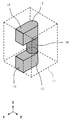
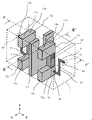
- FIG. 1 is a perspective view schematically showing a dielectric resonator according to a first embodiment of the present invention.
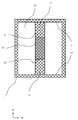
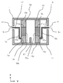
- FIG. 2 is a cross-sectional view taken along line A-A ′ of FIG. 1.
- FIG. 2 is a sectional view taken along line B-B ′ of FIG. 1.
- It is a perspective view which shows typically the dielectric resonator of 2nd Embodiment of this invention.
- It is a perspective view which shows typically the dielectric material filter of 3rd Embodiment of this invention.
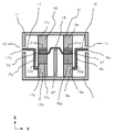
- FIG. 6 is a sectional view taken along line C-C ′ of FIG. 5.
- FIG. 6 is a sectional view taken along line D-D ′ of FIG. 5.
- FIG. 9 is a sectional view taken along line E-E ′ of FIG. 8.
- FIG. 9 is a cross-sectional view taken along the line F-F ′ of FIG. 8. It is a perspective view which shows typically the dielectric material filter of 5th Embodiment of this invention.
- FIG. 12 is a sectional view taken along line G-G ′ of FIG. 11.
- FIG. 12 is a sectional view taken along line H-H ′ of FIG. 11.
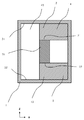
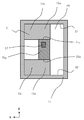
- FIG. 15 is a sectional view taken along line S-S ′ in FIG. 14.
- FIG. 15 is a sectional view taken along line K-K ′ of FIG. 14.
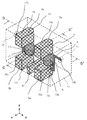
- FIG. 15 is a cross-sectional view taken along line M-M ′ of FIG. 14. It is a perspective view which shows typically the dielectric material filter of 7th Embodiment of this invention.
- FIG. 19 is a sectional view taken along line N-N ′ of FIG. 18.
- FIG. 19 is a cross-sectional view taken along the line P-P ′ of FIG. 18.
- FIG. 19 is a cross-sectional view taken along the line Q-Q ′ of FIG. 18.
- It is a block diagram which shows typically the communication apparatus of 8th Embodiment of this invention. It is a graph which shows the simulation result of the electrical property of the dielectric material filter of 3rd Embodiment of this invention.
- FIG. 29 is a sectional view taken along line J-J ′ of FIG. 28. It is a graph which shows the simulation result of the electrical property of the dielectric material filter of the 3rd comparative example.
- FIG. 1 is a perspective view schematically showing a dielectric resonator according to a first embodiment of the present invention.
- 2 is a cross-sectional view taken along line AA ′ of FIG. 3 is a cross-sectional view taken along the line BB ′ of FIG.
- FIG. 1 shows a state in which the conductor 11 is seen through in order to make the structure easy to understand.
- the dielectric resonator according to the present embodiment includes a conductor 11, a conductor 12, a conductor 13, a conductor 14, a conductor 15, and a dielectric 70.
- the dielectric 70 is a columnar dielectric extending in the first direction (+ z direction), and has a surface 21 located at the end in the + z direction and an end in the second direction ( ⁇ z direction) opposite to the + z direction. And a surface 22 located on the part.
- a material of the dielectric 70 a known dielectric material such as dielectric ceramics can be used.
- a dielectric ceramic material containing BaTiO 3 , Pb 4 Fe 2 Nb 2 O 12 , TiO 2 or the like can be preferably used.
- a resin such as an epoxy resin may be used.
- the case where the dielectric 70 is a quadrangular prism is shown, but it may be another shape such as a hexagonal prism or a cylinder.
- the conductor 11 has a rectangular parallelepiped box shape.
- the conductor 11 houses the dielectric 70 in a cavity 45 formed therein, and is disposed so as to surround the dielectric 70 with a gap.
- the conductor 11 includes an inner surface 31 having a portion facing the surface 21 and an inner surface 32 having a portion facing the surface 22.
- the case where the outer shape of the conductor 11 is a rectangular parallelepiped shape is shown, but other shapes such as a prism and a cylinder may be used.
- the conductor 12 is a columnar conductor extending in the + z direction.
- the conductor 12 is provided on the surface 21 of the dielectric 70.
- the end in the + z direction of the conductor 12 is electrically connected to the inner surface 31 of the conductor 11 by joining or contacting the inner surface 31 of the conductor 11.
- the conductor 13 is a columnar conductor extending in the + z direction.
- the conductor 13 is provided on the surface 22 of the dielectric 70.
- the end of the conductor 13 in the ⁇ z direction is electrically connected to the inner surface 32 of the conductor 11 by bonding or contacting the inner surface 32 of the conductor 11.
- the conductor 12 and the conductor 13 are quadrangular columns
- other shapes such as a hexagonal column and a cylinder, may be sufficient, for example.
- the conductor 12 and the conductor 13 desirably have the same cross-sectional shape as that of the dielectric 70 when cut along a plane perpendicular to the + z direction.
- the conductor 14 has a rectangular parallelepiped shape.
- the conductor 14 is disposed between the conductor 12 and the conductor 11 in the third direction (+ x direction) perpendicular to the + z direction.
- the end of the conductor 14 in the + x direction is electrically connected to the conductor 11 by joining or contacting the conductor 11.
- the end of the conductor 14 in the direction opposite to the + x direction ( ⁇ x direction) is electrically connected to the conductor 12 by bonding or contacting the conductor 12.
- the end of the conductor 14 in the + z direction is electrically connected to the inner surface 31 of the conductor 11 by joining or contacting the inner surface 31 of the conductor 11.
- the conductor 15 has a rectangular parallelepiped shape.
- the conductor 15 is disposed between the conductor 13 and the conductor 11 in the fourth direction (+ x direction) perpendicular to the + z direction.
- the end portion of the conductor 15 in the + x direction is electrically connected to the conductor 11 by joining or contacting the conductor 11.
- the end of the conductor 15 in the direction opposite to the + x direction ( ⁇ x direction) is electrically connected to the conductor 13 by bonding or contacting the conductor 13.
- the end of the conductor 15 in the ⁇ z direction is electrically connected to the inner surface 32 of the conductor 11 by joining or contacting the inner surface 32 of the conductor 11.
- the portions where the conductor 11, the conductor 12, the conductor 13, the conductor 14, and the conductor 15 are electrically connected to each other may be in electrical contact with each other, but are joined in terms of reliability. It is desirable. When joining, since it is necessary to join so that it may become electrically conductive, it may join using solder and a conductive adhesive, and may join using a screw, a volt
- the contact portion between the dielectric 70 and the conductor 12 and the contact portion between the dielectric 70 and the conductor 13 may be in electrical contact, but are desirably joined in terms of reliability. .
- it can join using a conductive adhesive.
- the first plate-like conductor is baked on the surface 21 of the dielectric 70
- the second plate-like conductor is baked on the surface 22 of the dielectric 70
- the first columnar conductor is attached to the first plate-like conductor.
- the second columnar conductor may be joined to the second plate-like conductor with solder or the like.
- the composite of the first plate-shaped conductor and the first columnar conductor corresponds to the conductor 12 in the present embodiment
- the composite of the second plate-shaped conductor and the second columnar conductor is the main. It corresponds to the conductor 13 in the embodiment.
- the conductors 11 to 15 can be formed using various known conductive materials such as metals and non-metal conductive materials.
- a conductive material mainly composed of an Ag alloy such as Ag, Ag—Pd, or Ag—Pt, or a Cu-based, W-based, Mo-based, Pd-based conductive material, or the like.
- the inside of the cavity 45 is filled with air, it may be a vacuum or may be filled with a gas other than air.
- the dielectric resonator according to the present embodiment having such a configuration is a spurious mode having the lowest resonance frequency compared to the conventional dielectric resonator having no conductors 12 to 15 described in Patent Document 1. Since the resonance frequency can be increased, a dielectric resonator having good electrical characteristics with a wide interval between the resonance frequency of the fundamental mode and the resonance frequency of the spurious mode can be obtained.
- the dielectric resonator of the present embodiment is different from the conventional dielectric resonator in the spurious mode having the lowest resonance frequency, and it is considered that this effect is obtained by changing the resonance mode.
- the dielectric resonator of the present embodiment since the dielectric resonator of the present embodiment includes the conductor 14 and the conductor 15, the Q value in the fundamental mode resonance is increased as compared with the case where the conductor 14 and the conductor 15 are not included. Can do. In the case where the conductor 14 and the conductor 15 are not provided, it is considered that a current loss is generated in the conductor 12 and the conductor 13 due to the magnetic field generated so as to surround the conductor 12 and the conductor 13, thereby reducing the Q value. In the dielectric resonator of the present embodiment, the magnetic field generated so as to surround the conductor 12 and the conductor 13 can be reduced by the conductor 14 and the conductor 15, so that it is considered that the current loss is reduced and the Q value is improved.
- the conductor 14 is between the conductor 12 and the conductor 11 in the third direction (+ x direction) and in the entire region between the dielectric 70 and the conductor 11 in the first direction (+ z direction). It is desirable to exist across.
- the conductor 15 is located between the conductor 13 and the conductor 11 in the fourth direction (+ x direction) and in the entire region between the dielectric 70 and the conductor 11 in the first direction (+ z direction). It is desirable to exist across. Thereby, the Q value in the fundamental mode resonance can be improved.
- the third direction and the fourth direction coincide with each other. That is, the direction in which the conductor 14 is located with respect to the conductor 12 is coincident with the direction in which the conductor 15 is located with respect to the conductor 13. Thereby, it is possible to obtain a dielectric resonator that can be easily electromagnetically coupled to other resonators.
- FIG. 4 is a perspective view schematically showing a dielectric resonator according to the second embodiment of the present invention.
- FIG. 4 shows a state where the conductor 11 is seen through in order to make the structure easy to understand.
- a different part from 1st Embodiment mentioned above is demonstrated, the same code
- the dielectric 70, the conductor 12, and the conductor 13 have a cylindrical shape.
- the conductor 14 and the conductor 15 have the shape which removed the cylinder from the rectangular parallelepiped.
- Other configurations are all the same as those of the resonator according to the first embodiment described above.
- the dielectric resonator according to the present embodiment has the same configuration as the dielectric resonator according to the first embodiment described above, and has the same superiority as the dielectric resonator according to the first embodiment described above. It has electrical characteristics.
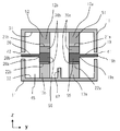
- FIG. 5 is a perspective view schematically showing a dielectric filter according to a third embodiment of the present invention.
- 6 is a cross-sectional view taken along the line CC ′ of FIG. 7 is a cross-sectional view taken along the line DD ′ of FIG.
- FIG. 5 shows a state in which the conductor 11 is seen through in order to make the structure easy to understand.
- a different part from 2nd Embodiment mentioned above is demonstrated, the same code
- a plurality of sets each including the dielectric 70, the conductor 12, the conductor 13, the conductor 14, and the conductor 15 are provided in the cavity 45.
- the plurality of sets are arranged so as to form a row.
- the first set 51 is a set located at one end of the row (the end in the + y direction) and the other end of the row (the end in the ⁇ y direction).
- a second set 52 which is a set located in the position.
- Each of the plurality of sets (the first set 51 and the second set 52) functions as a resonator together with the conductor 11.
- the first set 51 includes a dielectric 70a, a conductor 12a, a conductor 13a, a conductor 14a, and a conductor 15a.
- the second set 52 includes a dielectric 70b, a conductor 12b, a conductor 13b, a conductor 14b, and a conductor 15b.
- the dielectric 70a and the dielectric 70b are the same as the dielectric 70 in the second embodiment.
- the conductor 12a and the conductor 12b are the same as the conductor 12 in the second embodiment.
- the conductor 13a and the conductor 13b are the same as the conductor 13 in the second embodiment.
- the conductors 14a and 14b are the same as the conductors 14 in the second embodiment.
- the conductor 15a and the conductor 15b are the same as the conductor 15 in the second embodiment. That is, each of the resonator constituted by the first set 51 and the conductor 11 and the resonator constituted by the second set 52 and the conductor 11 have the same configuration as the resonator of the second embodiment described above. And has excellent electrical characteristics similar to those of the resonator according to the second embodiment.
- the dielectric filter of the present embodiment further has a conductor 16 which is a linear conductor.
- the conductor 16 has an end portion 16a which is one end, an end portion 16b which is the other end, and a coupling portion 16c which is a portion extending in the + z direction along the dielectric 70a.
- the end portion 16a is connected to the conductor 13a, and the end portion 16b is exposed to the outside through the through hole 41 formed in the conductor 11. Note that the end portion 16a may be connected to the conductor 12a.
- the dielectric filter of the present embodiment further includes a conductor 17 that is a linear conductor.
- the conductor 17 has an end portion 17a which is one end, an end portion 17b which is the other end, and a coupling portion 17c which is a portion extending in the + z direction along the dielectric 70b.
- the end portion 17a is connected to the conductor 13b, and the end portion 17b is exposed to the outside through the through hole 42 formed in the conductor 11. Note that the end portion 17a may be connected to the conductor 12b.
- the coupling portion 16c and the coupling portion 17c are preferably formed in parallel to the + z direction, but may be slightly inclined with respect to the + z direction. Further, it is desirable that the coupling portion 16c is located closer to the dielectric 70a than the center in the space between the dielectric 70a and the conductor 11. Thereby, the coupling part 16c and the dielectric 70a can be electromagnetically coupled satisfactorily. Similarly, it is desirable that the coupling portion 17c is located closer to the dielectric 70b than the center in the space between the dielectric 70b and the conductor 11. Thereby, the coupling
- the dielectric filter of this embodiment further has a conductor 47.
- the conductor 47 is disposed between the first set 51 and the second set 52 in the + y direction.
- the conductor 47 has an end in the ⁇ z direction joined to the inner surface 32 of the conductor 11 and is formed at a lower height than the conductors 13a and 13b and over the entire + x direction.
- the conductor 47 can adjust the coupling between the dielectric 70a and the dielectric 70b.
- the conductor 47 is not essential and may be omitted depending on circumstances.
- each resonator when an electric signal is input from the end 16b of the conductor 16, each resonator resonates and the electric signal is output from the end 17b of the conductor 17. Is output. At this time, since a signal in a frequency band including the resonance frequency of each resonator selectively passes, it functions as a bandpass filter.
- the dielectric filter of this embodiment uses a dielectric resonator having a high Q value in the resonance of the fundamental mode and having good electrical characteristics with a wide interval between the resonance frequency of the fundamental mode and the resonance frequency of the spurious mode. Configure the filter. Thereby, it is possible to obtain excellent electrical characteristics with a small insertion loss in the pass band and a large attenuation near the pass band.
- the dielectric filter of the present embodiment includes a third direction (+ x direction) in which the conductors 14a and 14b are arranged, and a fourth direction (+ x direction) in which the conductors 15a and 15b are arranged. ), And a plurality of sets are arranged along the fifth direction (+ y direction) perpendicular to both the first direction (+ z direction) and the third direction (+ x direction).
- the number of sets is preferably about 10 or less.
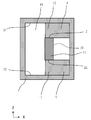
- FIG. 8 is a perspective view schematically showing a dielectric filter according to a fourth embodiment of the present invention.
- 9 is a cross-sectional view taken along the line EE ′ of FIG. 10 is a cross-sectional view taken along line FF ′ of FIG.
- FIG. 8 shows a state in which the conductor 11 is seen through for easy understanding of the structure.
- a different part from the above-described third embodiment will be described, and the same constituent elements will be denoted by the same reference numerals and redundant description will be omitted.
- the dielectric 70a, the conductor 12a, and the conductor 13a have a quadrangular columnar shape
- the dielectric 70b, the conductor 12b, and the conductor 13b have a quadrangular columnar shape
- the conductor 14a and the conductor 15a have a rectangular parallelepiped shape
- the conductor 14b and the conductor 15b have a rectangular parallelepiped shape.
- the dielectric filter of the present embodiment includes the electrode 57, the electrode 58, and the conductor 18.
- the electrode 57 is disposed in the dielectric 70a so as to be biased toward the conductor 12a.
- the electrode 58 is disposed in the dielectric 70b so as to be biased toward the conductor 12b.
- the conductor 18 is a linear conductor. One end of the conductor 18 is joined to the electrode 57, and the other end of the conductor 18 is joined to the electrode 58. That is, the conductor 18 connects the electrode 57 and the electrode 58.
- the electrode 57 may be disposed in the dielectric 70a so as to be biased toward the conductor 13a
- the electrode 58 may be disposed in the dielectric 70b so as to be biased toward the conductor 13b.
- the conductor 47 is disposed so as to partition the first set 51 and the second set 52 almost entirely.
- the conductor 18 is disposed so as to pass through a recess formed at the end in the + z direction of the conductor 47 so as not to contact the conductor 47.
- the dielectric filter of the present embodiment includes the electrode 57, the electrode 58, and the conductor 18.
- the electrode 57 is disposed in the dielectric 70a so as to be biased toward one side of the conductor 12a and the conductor 13a.
- the electrode 58 is disposed in the dielectric 70b so as to be biased toward one side of the conductor 12b and the conductor 13b.
- the conductor 18 connects the electrode 57 and the electrode 58.
- the dielectric filter of this embodiment having such a configuration can capacitively couple the first set 51 and the second set 52 by the conductor 18, so that it is compared with the dielectric filter of the third embodiment described above. Thus, it is possible to increase the amount of attenuation on the higher frequency side than the pass band.
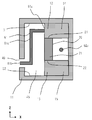
- FIG. 11 is a perspective view schematically showing a dielectric filter according to a fifth embodiment of the present invention. 12 is a cross-sectional view taken along the line GG ′ of FIG. 13 is a cross-sectional view taken along the line HH ′ of FIG. Note that FIG. 11 shows a state where the conductor 11 is seen through in order to make the structure easy to understand. Further, in the present embodiment, portions different from those of the third embodiment described above will be described, and the same constituent elements will be denoted by the same reference numerals, and redundant description will be omitted.
- the dielectric 70a, the conductor 12a, and the conductor 13a have a quadrangular columnar shape
- the dielectric 70b, the conductor 12b, and the conductor 13b have a quadrangular columnar shape
- the conductor 14a and the conductor 15a have a rectangular parallelepiped shape
- the conductor 14b and the conductor 15b have a rectangular parallelepiped shape.
- the dielectric filter of the present embodiment has a conductor 19 instead of the conductor 16, and a conductor 20 instead of the conductor 17. Further, the dielectric filter of the present embodiment has an electrode 55 and an electrode 56.
- the electrode 55 is disposed in the dielectric 70a so as to be biased toward one side of the conductor 12a and the conductor 13a.
- the electrode 55 has a function of generating an electric field in the dielectric 70a when an electric signal is supplied through the conductor 19.
- the electrode 56 is disposed in the dielectric 70b so as to be biased toward one side of the conductor 12b and the conductor 13b.
- the electrode 56 has a function of generating an electric field in the dielectric 70a when an electric signal is supplied through the conductor 20.
- FIGS. 11 to 13 show an example in which the electrode 55 is arranged biased toward the conductor 13a ( ⁇ z direction) and the electrode 56 is biased arranged toward the conductor 13b ( ⁇ z direction).
- the electrode 55 may be arranged biased toward the conductor 12a (+ z direction side), and the electrode 56 may be arranged biased toward the conductor 12b side (+ z direction side).
- the conductor 19 is a linear conductor, and has an end 19a that is one end and an end 19b that is the other end.
- the end portion 19 a is connected to the electrode 55, and the end portion 19 b is exposed to the outside through the through hole 41 formed in the conductor 11.
- the conductor 20 is a linear conductor and has an end 20a that is one end and an end 20b that is the other end.
- the end portion 20 a is connected to the electrode 56, and the end portion 20 b is exposed to the outside through the through hole 42 formed in the conductor 11.
- the two resonators when an electric signal is input from the end 19b of the conductor 19, the two resonators resonate and the electric signal is output from the end 20b of the conductor 20. Is output. At this time, since a signal in a frequency band including the resonance frequency of the two resonators selectively passes, it functions as a band-pass filter.
- the dielectric filter of the present embodiment is configured using a resonator having a high Q value in the resonance of the fundamental mode and a wide interval between the resonance frequency of the fundamental mode and the resonance frequency of the spurious mode. Thereby, it is possible to obtain excellent electrical characteristics with a small insertion loss in the pass band and a large attenuation near the pass band.
- the third direction (+ x direction) which is the direction in which the conductors 14a and 14b are arranged, and the fourth direction (+ x direction), in which the conductors 15a and 15b are arranged.
- a plurality of sets are arranged along the fifth direction (+ y direction) perpendicular to both the first direction (+ z direction) and the third direction (+ x direction).
- the third direction and the fourth direction do not necessarily coincide with each other.
- the third direction and the fourth direction may be opposite to each other.
- the electrode 55 is biased in one of the first direction and the second direction (the second direction ( ⁇ z direction in FIGS. 11 to 13)) in the dielectric 70a.
- the end 19a of the conductor 19 is connected to the other side of the electrode 55 in the first direction and the second direction (the first direction (+ z direction in FIGS. 11 to 13)).
- the electromagnetic coupling between the electrode 55 and the dielectric 70a can be strengthened. It is to be noted that the same effect can be obtained even when the electrode 55 is disposed in the dielectric 70a so as to be biased in the + z direction and the end 19a of the conductor 19 is connected to the ⁇ z direction side of the electrode 55. be able to.
- the electrode 56 is biased in one of the first direction and the second direction (the second direction ( ⁇ z direction in FIGS. 11 to 13)) in the dielectric 70b.
- the end 20a of the conductor 20 is connected to the other side of the electrode 56 in the first direction and the second direction (the first direction (+ z direction in FIGS. 11 to 13)).
- the electromagnetic coupling between the electrode 56 and the dielectric 70b can be strengthened. It is to be noted that the same effect can be obtained even when the electrode 56 is disposed in the dielectric 70b so as to be biased in the + z direction and the end portion 20a of the conductor 20 is connected to the ⁇ z direction side of the electrode 56. be able to.
- FIG. 14 is a perspective view schematically showing a dielectric resonator according to a sixth embodiment of the present invention.
- 15 is a cross-sectional view taken along the line SS ′ of FIG. 14 (a cut surface parallel to the xz plane including the SS ′ line (a cut surface that bisects the conductor 11 in the + y direction) viewed from the ⁇ y direction.
- Figure 16 is a cross-sectional view taken along the line KK ′ of FIG. 14 (a cut surface parallel to the xy plane including the line KK ′ (a cut surface that bisects the conductor 11 in the + z direction) viewed from the + z direction. ).
- FIG. 17 is a cross-sectional view taken along line MM ′ in FIG. 14 (a cut surface parallel to the yz plane including the MM ′ line (a cut surface that equally bisects the conductor 11 in the + x direction) viewed from the + x direction. ).
- the conductor 11 is seen through in order to make the structure easy to understand. Further, in the present embodiment, parts different from those of the first embodiment described above will be described, and the same constituent elements will be denoted by the same reference numerals and redundant description will be omitted.
- the dielectric resonator according to the present embodiment includes a conductor 26, a conductor 27, a conductor 28, and a conductor 29 as shown in FIGS.
- the dielectric 70 has a shape (a cross shape) in which the first portion 71 and the second portion 72 intersect each other.
- the first portion 71 is a columnar portion extending in the first direction (+ z direction), the surface 21 located at the end of the first direction (+ z direction), and the second direction (the direction opposite to the first direction). And a surface 22 located at the end in the ⁇ z direction).
- the second portion 72 is a columnar portion extending in a fifth direction ( ⁇ y direction) perpendicular to the first direction, the surface 23 located at the end of the fifth direction ( ⁇ y direction), the fifth direction, And a surface 24 located at the end of the sixth direction (+ y direction) which is the opposite direction.
- the conductor 26 is a columnar conductor extending in the -y direction.
- the conductor 26 is provided on the surface 23 of the dielectric 70.
- An end portion of the conductor 26 in the fifth direction ( ⁇ y direction) is electrically connected to the inner surface 33 of the conductor 11 by joining or contacting the inner surface 33 of the conductor 11.
- the conductor 27 is a columnar conductor extending in the ⁇ y direction.
- the conductor 27 is provided on the surface of the dielectric 70.
- the end portion of the conductor 27 in the sixth direction (+ y direction) is electrically connected to the inner surface 34 of the conductor 11 by joining or contacting the inner surface 34 of the conductor 11.
- the conductor 28 has a rectangular parallelepiped shape.
- the conductor 28 is disposed between the conductor 26 and the conductor 11 in the seventh direction ( ⁇ x direction) perpendicular to the first direction and the fifth direction.
- An end portion of the conductor 28 in the seventh direction ( ⁇ x direction) is electrically connected to the conductor 11 by bonding or contacting the conductor 11.
- the end of the conductor 28 in the direction opposite to the seventh direction (+ x direction) is electrically connected to the conductor 26 by joining or contacting the conductor 26.
- the end portion of the conductor 28 in the fifth direction ( ⁇ y direction) is electrically connected to the inner surface 33 of the conductor 11 by joining or contacting the inner surface 33 of the conductor 11.
- the conductor 29 has a rectangular parallelepiped shape.
- the conductor 29 is disposed between the conductor 27 and the conductor 11 in the seventh direction ( ⁇ x direction).
- An end portion of the conductor 29 in the seventh direction ( ⁇ x direction) is electrically connected to the conductor 11 by joining or contacting the conductor 11.
- the end of the conductor 29 in the direction opposite to the seventh direction (+ x direction) is electrically connected to the conductor 27 by joining or contacting the conductor 27.
- the end portion of the conductor 29 in the sixth direction (+ y direction) is electrically connected to the inner surface 34 of the conductor 11 by joining or contacting the inner surface 34 of the conductor 11.
- a groove 75 is formed in the dielectric 70.
- the groove 75 is formed at a portion where the first portion 71 and the second portion 72 intersect and is formed over the entire + x direction.
- Such a groove 75 has a function of releasing the degeneration of the two resonance modes, and the shape of the groove 75 is appropriately adjusted according to desired characteristics.
- the conductor 12, the conductor 13, the conductor 26, and the conductor 27 are quadrangular columns is shown in this embodiment, other shapes such as a hexagonal column or a cylinder may be used. However, it is desirable that the conductor 26 and the conductor 27 have the same cross-sectional shape as that of the second portion 72 when cut along a plane perpendicular to the ⁇ y direction.
- the materials and configurations of the conductors 26 to 29 (conductor 26, conductor 27, conductor 28, conductor 29) and the joining state with adjacent portions are as follows: ). 14 to 17 show a case where the conductor 26 and the conductor 28 are integrally formed, and the conductor 27 and the conductor 29 are integrally formed.
- the dielectric resonator of this embodiment having such a configuration functions as a dual mode resonator.
- the dielectric resonator according to the present embodiment includes the conductor 12, the conductor 13, the conductor 26, and the conductor 27, the resonance frequency of the fundamental mode and the resonance frequency of the spurious mode in both of the two modes. The interval can be increased.
- the dielectric resonator of the present embodiment includes the conductor 14, the conductor 15, the conductor 28, and the conductor 29, it is compared with the case where the conductor 14, the conductor 15, the conductor 28, and the conductor 29 are not included. Thus, the Q value in the fundamental mode resonance can be increased.
- the conductor 28 is located between the conductor 26 and the conductor 11 on the seventh direction ( ⁇ x direction) side of the conductor 26, and in the fifth direction ( ⁇ y direction). It is desirable to exist over the entire region between the surface 23 and the inner surface 33.
- the conductor 29 is between the conductor 27 and the conductor 11 on the seventh direction ( ⁇ x direction) side of the conductor 27, and between the surface 24 and the inner surface 34 in the fifth direction ( ⁇ y direction). It is desirable to exist throughout the area. As a result, the magnetic field generated so as to surround the conductor 26 and the conductor 27 can be further reduced, so that the current loss in the conductor 26 and the conductor 27 can be further reduced and the Q value can be further improved.
- the third direction (+ x direction) and the seventh direction ( ⁇ x direction) are opposite to each other. That is, the direction in which the conductor 14 and the conductor 15 are positioned with respect to the conductor 12 and the conductor 13 and the direction in which the conductor 28 and the conductor 29 are positioned with respect to the conductor 26 and the conductor 27 are opposite directions.
- the direction in which the conductor 14 and the conductor 15 are positioned with respect to the conductor 12 and the conductor 13 and the direction in which the conductor 28 and the conductor 29 are positioned with respect to the conductor 26 and the conductor 27 are opposite directions.
- FIG. 18 is a perspective view schematically showing a dielectric filter according to a seventh embodiment of the present invention.
- 19 is a cross-sectional view taken along line NN ′ of FIG. 18 (a view of a cut surface parallel to the xz plane including the line NN ′ viewed from the ⁇ y direction).
- 20 is a cross-sectional view taken along the line PP ′ of FIG. 18 (a view of a cut surface parallel to the xy plane including the line PP ′ viewed from the + z direction).
- 21 is a cross-sectional view taken along the line QQ ′ of FIG. 18 (a view of a cut surface parallel to the yz plane including the QQ ′ line viewed from the + x direction). Note that FIG.
- the dielectric filter of the present embodiment includes the dielectric resonator of the sixth embodiment described above, a conductor 61, and a conductor 62.
- the conductor 61 is a linear conductor, and is an end portion 61a that is one end, an end portion 61b that is the other end, and a coupling portion that is a portion extending in the first direction (+ z direction) along the first portion 71. 61c.
- the coupling portion 61c is a portion that is coupled to the first portion 71 mainly by a magnetic field.
- the conductor 61 is electromagnetically coupled to the first portion 71.
- the end portion 61 a is connected to the conductor 12, and the end portion 61 b is exposed to the outside through a through hole 49 formed in the conductor 11. Note that the end 61 a may be connected to the conductor 13 instead of the conductor 12.
- the conductor 62 is a linear conductor, and is a coupling that is an end portion 62a that is one end, an end portion 62b that is the other end, and a portion that extends in the fifth direction ( ⁇ y direction) along the second portion 72. Part 62c.
- the coupling portion 62c is a portion that couples with the second portion 72 mainly by a magnetic field.
- the conductor 62 is electromagnetically coupled to the first portion 72.
- the end 62 a is connected to the conductor 26, and the end 62 b is exposed to the outside through the through hole 48 formed in the conductor 11. Note that the end portion 62 a may be connected to the conductor 27 instead of the conductor 26.
- the coupling portion 61c is desirably formed in parallel to the + z direction, but may have a component in the + z direction and may be inclined with respect to the + z direction.
- the coupling portion 62c is desirably formed in parallel with the -y direction, but may have a component in the -y direction and may be inclined with respect to the -y direction. Further, the positions and lengths of the coupling portion 61c and the coupling portion 62c can be appropriately adjusted according to the desired magnitude of magnetic field coupling.
- the dielectric filter of this embodiment having such a configuration, for example, when an electric signal is input from the end 61 b of the conductor 61, the dielectric 70 resonates and an electric signal is output from the end 62 b of the conductor 62. Is done. At this time, since a signal in a frequency band including the resonance frequencies of the first resonance mode, the second resonance mode, and the third resonance mode described above selectively passes, it functions as a bandpass filter.
- the dielectric filter of this embodiment uses a dielectric resonator having a high Q value in the resonance of the fundamental mode and having good electrical characteristics with a wide interval between the resonance frequency of the fundamental mode and the resonance frequency of the spurious mode. Configure the filter. Thereby, it is possible to obtain a dielectric filter having excellent electrical characteristics with a small insertion loss in the pass band and a large attenuation near the pass band.
- FIG. 22 is a block diagram schematically showing a communication device according to the eighth embodiment of the present invention.
- the communication device of this embodiment includes an antenna 82, a communication circuit 81, and a dielectric filter 80 that connects the antenna 82 and the communication circuit 81.
- the dielectric filter 80 is the dielectric filter of the third embodiment described above.
- the antenna 82 and the communication circuit 81 are well-known conventional ones.
- the communication apparatus of this embodiment having such a configuration removes unnecessary electrical signals using the dielectric filter of the third embodiment with good electrical characteristics, a communication apparatus with good communication quality can be obtained. it can.
- the dielectric filter of the third embodiment In place of the dielectric filter of the third embodiment, the dielectric filter of the fourth embodiment, the dielectric filter of the fifth embodiment, the dielectric filter of the seventh embodiment, and other forms of dielectrics A filter may be used.
- the electrical characteristics of the dielectric resonator according to the first embodiment shown in FIGS. 1 to 3 were calculated by simulation.
- the dielectric constituting the dielectric 70 has a relative dielectric constant of 60 and a dielectric loss tangent of 0.00005.
- the electric conductivity of various conductors was 46.4 ⁇ 10 6 S / m.
- the inner shape of the conductor 11 (the outer shape of the cavity 45) was a rectangular parallelepiped having a dimension in the + x direction of 20 mm, a dimension in the + y direction of 20 mm, and a dimension in the + z direction of 24 mm.
- the dielectric 70 has a columnar shape with a dimension in the + x direction of 4.4 mm, a dimension in the + y direction of 4.4 mm, and a dimension in the + z direction of 10 mm.
- the size in the + x direction and the size in the + y direction of the conductor 12 and the conductor 13 are the same as those of the dielectric 70.
- the conductor 12 and the conductor 13 have the same shape, and the conductor 14 and the conductor 15 have the same shape.
- the resonance frequency of the fundamental mode was 2.077 GHz
- the Q value was 3540
- the resonance frequency of the lowest spurious mode was 5.790 GHz.
- the electrical characteristics of the dielectric resonator of the first comparative example shown in FIG. 25 were calculated by simulation.
- the dielectric resonator of the first comparative example has a shape in which the conductor 14 and the conductor 15 are removed from the dielectric resonator of the first embodiment.
- the dimension in the + x direction and the dimension in the + y direction of the dielectric 70 are set to 3.6 mm.
- the resonance frequency of the fundamental mode was 2.037 GHz
- the Q value was 3199
- the resonance frequency of the lowest spurious mode was 6.273 GHz.
- the electrical characteristics of the dielectric resonator of the second comparative example shown in FIG. 26 were calculated by simulation.
- the dielectric resonator of the second comparative example has a shape in which the conductor 12, the conductor 13, the conductor 14, and the conductor 15 are removed from the dielectric resonator of the first embodiment. This shape is that of a conventional dielectric resonator.
- the dimension in the + y direction and the dimension in the + x direction of the dielectric 70 are set to 6.5 mm, and the dimension in the + z direction of the cavity 45 and the dielectric 70 is set to 10 mm.
- the resonance frequency of the fundamental mode was 2.044 GHz
- the Q value was 4000
- the resonance frequency of the lowest spurious mode was 4.200 GHz.
- the resonator of the second comparative example which is a conventional resonator has a big problem that the resonance frequency of the spurious mode having the lowest frequency is low, and the dielectric resonance of the first comparative example.
- This device has a big problem that the Q value of the fundamental mode resonance is low.
- the dielectric resonator according to the first embodiment has a high Q value of the fundamental mode resonance and a high resonance frequency of the spurious mode having the lowest frequency, and has excellent electric characteristics that are balanced and free from defects. Have. Thereby, the effect of the present invention can be confirmed.
- the electrical characteristics of the dielectric filter of the third embodiment shown in FIGS. 5 to 7 were calculated by simulation.
- the dielectric constituting the dielectric 70 has a relative dielectric constant of 60 and a dielectric loss tangent of 0.00005.
- the electric conductivity of various conductors was 46.4 ⁇ 10 6 S / m.
- the inner shape of the conductor 11 (the outer shape of the cavity 45) was a rectangular parallelepiped having a dimension in the + x direction of 20 mm, a dimension in the + y direction of 42 mm, and a dimension in the + z direction of 26 mm.
- the dielectric 70a and the dielectric 70b have a cylindrical shape with a diameter of 6 mm and a dimension in the + z direction of 10 mm.
- the size in the + x direction and the size in the + y direction of the conductor 12a, the conductor 12b, the conductor 13a, and the conductor 13b are the same as those of the dielectric 70a and the dielectric 70b.
- the conductor 12a, the conductor 12b, the conductor 13a, and the conductor 13b have the same shape, and the conductor 14a, the conductor 14b, the conductor 15a, and the conductor 15b have the same shape.
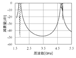
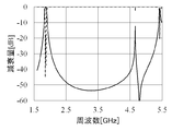
- the result of the simulation is shown in the graph of FIG.
- the horizontal axis represents frequency and the vertical axis represents attenuation. According to the graph, it can be seen that excellent electrical characteristics with a small insertion loss in the pass band and a large attenuation near the pass band are obtained. The effectiveness of the present invention can also be confirmed from this graph.
- the electrical characteristics of the dielectric filter of the fourth embodiment shown in FIGS. 8 to 10 were calculated by simulation.
- the dielectric constituting the dielectric 70 has a relative dielectric constant of 60 and a dielectric loss tangent of 0.00005.
- the electric conductivity of various conductors was 46.4 ⁇ 10 6 S / m.
- the inner shape of the conductor 11 (the outer shape of the cavity 45) was a rectangular parallelepiped having a dimension in the + x direction of 20 mm, a dimension in the + y direction of 42 mm, and a dimension in the + z direction of 26 mm.
- the dielectric body 70a and the dielectric body 70b were formed in a rectangular column shape having a dimension in the + x direction of 4.4 mm, a dimension in the + y direction of 4.4 mm, and a dimension in the + z direction of 10 mm.
- the size in the + x direction and the size in the + y direction of the conductor 12a, the conductor 12b, the conductor 13a, and the conductor 13b are the same as those of the dielectric 70a and the dielectric 70b.
- the conductor 12a, the conductor 12b, the conductor 13a, and the conductor 13b have the same shape, and the conductor 14a, the conductor 14b, the conductor 15a, and the conductor 15b have the same shape.
- the horizontal axis represents frequency and the vertical axis represents attenuation. According to the graph, it can be seen that excellent electrical characteristics are obtained in which the insertion loss in the pass band is small and the attenuation amount on the high frequency side is larger than that in the pass band. The effectiveness of the present invention can also be confirmed from this graph.
- the electrical characteristics of the dielectric filter of the fifth embodiment shown in FIGS. 11 to 13 were calculated by simulation.
- the dielectric constituting the dielectric 70 has a relative dielectric constant of 60 and a dielectric loss tangent of 0.00005.
- Conductivity of various conductors (conductor 11, conductor 12a, conductor 12b, conductor 13a, conductor 13b, conductor 14a, conductor 14b, conductor 15a, conductor 15b, conductor 19, conductor 20), electrode 55 and electrode 56 is 46.4 ⁇ . 10 6 S / m.
- the inner shape of the conductor 11 (the outer shape of the cavity 45) was a rectangular parallelepiped having a width (size in the + x direction) 20 mm, a length (size in the + y direction) 42 mm, and a height (size in the + z direction) 26 mm.
- the dielectric 70a and the dielectric 70b were formed in a quadrangular prism shape having a length of 3.9 mm, a width of 3.9 mm, and a height of 10 mm.
- the length and width of the conductor 12a, the conductor 12b, the conductor 13a, and the conductor 13b are the same as those of the dielectric 70a and the dielectric 70b.
- the conductor 12a, the conductor 12b, the conductor 13a, and the conductor 13b have the same shape, and the conductor 14a, the conductor 14b, the conductor 15a, and the conductor 15b have the same shape. The result is shown in the graph of FIG.
- FIG. 28 is a perspective view schematically showing a dielectric filter of a third comparative example.
- 29 is a cross-sectional view taken along line J-J ′ of FIG.
- FIG. 28 shows a state where the conductor 11 is seen through in order to make the structure easy to understand.
- the dielectric filter of the third comparative example is different from the dielectric filter of the fifth embodiment shown in FIGS.
- the inner shape of the conductor 11 was a rectangular parallelepiped having a width of 20 mm, a length of 42 mm, and a height of 10 mm.
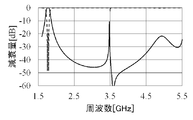
- the dielectric 70a and the dielectric 70b were in the shape of a rectangular column having a length of 7.8 mm, a width of 7.8 mm, and a height of 10 mm. The result is shown in the graph of FIG.
- the horizontal axis indicates the frequency
- the vertical axis indicates the attenuation.
- a peak due to spurious mode resonance occurs in the vicinity of 3.5 GHz near the passband, and the attenuation near the passband is insufficient. Recognize.
- the insertion loss of the pass band is small, and the peak due to the spurious mode resonance is shifted to the high frequency side. It can be seen that excellent electrical properties are obtained with a large amount. Also from this result, the effectiveness of the present invention can be confirmed.
- Electrode 70 Dielectric 71: First part 72: Second part 80: Dielectric filter 81: Communication circuit 82: Antenna
Landscapes
- Control Of Motors That Do Not Use Commutators (AREA)
Abstract
Description
図1は、本発明の第1実施形態の誘電体共振器を模式的に示す斜視図である。図2は、図1のA-A’線断面図である。図3は、図1のB-B’線断面図である。なお、図1においては、構造をわかりやすくするために、導体11を透視した状態を示している。本実施形態の誘電体共振器は、図1~図3に示すように、導体11と、導体12と、導体13と、導体14と、導体15と、誘電体70とを有している。
図4は、本発明の第2実施形態の誘電体共振器を模式的に示す斜視図である。なお、図4においては、構造をわかりやすくするために、導体11を透視した状態を示している。また、本実施形態においては、上述した第1実施形態と異なる部分について説明し、同様の構成要素には同様の符号を付して重複する説明を省略する。
図5は、本発明の第3実施形態の誘電体フィルタを模式的に示す斜視図である。図6は、図5のC-C’線断面図である。図7は、図5のD-D’線断面図である。なお、図5においては、構造をわかりやすくするために、導体11を透視した状態を示している。また、本実施形態においては、上述した第2実施形態と異なる部分について説明し、同様の構成要素には同様の符号を付して重複する説明を省略する。
図8は、本発明の第4実施形態の誘電体フィルタを模式的に示す斜視図である。図9は、図8のE-E’線断面図である。図10は、図8のF-F’線断面図である。なお、図8においては、構造をわかりやすくするために、導体11を透視した状態を示している。また、本実施形態においては、前述した第3実施形態と異なる部分について説明し、同様の構成要素には同様の符号を付して重複する説明を省略する。
図11は、本発明の第5実施形態の誘電体フィルタを模式的に示す斜視図である。図12は、図11のG-G’線断面図である。図13は、図11のH-H’線断面図である。なお、図11においては、構造をわかりやすくするために、導体11を透視した状態を示している。また、本実施形態においては、前述した第3実施形態と異なる部分について説明し、同様の構成要素には同様の符号を付して重複する説明を省略する。
図14は、本発明の第6実施形態の誘電体共振器を模式的に示す斜視図である。図15は、図14のS-S’線断面図(S-S’線を含むxz平面に平行な切断面(導体11を+y方向に2等分する切断面)を-y方向から見た図)である。図16は、図14のK-K’線断面図(K-K’線を含むxy平面に平行な切断面(導体11を+z方向に2等分する切断面)を+z方向から見た図)である。図17は、図14のM-M’線断面図(M-M’線を含むyz平面に平行な切断面(導体11を+x方向に2等分する切断面)を+x方向から見た図)である。なお、図14においては、構造をわかりやすくするために、導体11を透視した状態を示している。また、本実施形態においては、前述した第1実施形態と異なる部分について説明し、同様の構成要素には同様の符号を付して重複する説明を省略する。
図18は、本発明の第7実施形態の誘電体フィルタを模式的に示す斜視図である。図19は、図18のN-N’線断面図(N-N’線を含むxz平面に平行な切断面を-y方向から見た図)である。図20は、図18のP-P’線断面図(P-P’線を含むxy平面に平行な切断面を+z方向から見た図)である。図21は、図18のQ-Q’線断面図(Q-Q’線を含むyz平面に平行な切断面を+x方向から見た図)である。なお、図18においては、構造をわかりやすくするために、導体11を透視した状態を示している。また、本実施形態においては、上述した第6実施形態と異なる部分について説明し、同様の構成要素には同様の符号を付して重複する説明を省略する。本実施形態の誘電体フィルタは、図18~図21に示すように、前述した第6実施形態の誘電体共振器と、導体61と、導体62とを有している。
図22は、本発明の第8実施形態の通信装置を模式的に示すブロック図である。本実施形態の通信装置は、アンテナ82と、通信回路81と、アンテナ82と通信回路81とを接続する誘電体フィルタ80とを有している。誘電体フィルタ80は、前述した第3実施形態の誘電体フィルタである。アンテナ82および通信回路81は、既知の従来のものである。
41,42,48,49:貫通孔
45:空洞
55,56,57,58:電極
70:誘電体
71:第1部分
72:第2部分
80:誘電体フィルタ
81:通信回路
82:アンテナ
Claims (14)
- 第1方向の端部に位置する第1表面と、前記第1方向と反対方向である第2方向の端部に位置する第2表面とを有する誘電体と、
内部に形成された空洞内に前記誘電体を収容し、間隔を開けて前記誘電体を取り囲むように配置されており、前記第1表面と対向する部分を有する第1内面と、前記第2表面と対向する部分を有する第2内面と、を有する第1導体と、
前記第1表面に設けられており、前記第1方向の端部が、前記第1内面に電気的に接続された第2導体と、
前記第2表面に設けられており、前記第2方向の端部が、前記第2内面に電気的に接続された第3導体と、
前記第1方向に垂直な第3方向において前記第2導体と前記第1導体との間に配置されており、前記第1方向の端部および前記第3方向の端部が前記第1導体に電気的に接続されており、前記第3方向と反対方向の端部が前記第2導体に電気的に接続された第4導体と、
前記第1方向に垂直な第4方向において前記第3導体と前記第1導体との間に配置されており、前記第4方向の端部および前記第2方向の端部が前記第1導体に電気的に接続されており、前記第4方向と反対方向の端部が前記第3導体に電気的に接続された第5導体と、
を有することを特徴とする誘電体共振器。 - 前記第3方向と前記第4方向とが一致していることを特徴とする請求項1に記載の誘電体共振器。
- 請求項1に記載の誘電体共振器において、前記誘電体,前記第2導体,前記第3導体,前記第4導体および前記第5導体で構成される組が、前記空洞の中に複数設けられているとともに、複数の前記組が列を成すように配置されており、前記列の一方端に位置する前記組である第1組と、前記列の他方端に位置する前記組である第2組とを少なくとも有しており、
一方端である第1端部と、他方端である第2端部と、を有する線状の導体であり、前記第1端部が前記第1組における前記第2導体または前記第3導体に接続されており、前記第2端部が前記第1導体に設けられた第1の貫通孔を介して外部へ露出しており、前記第1組における前記誘電体と電磁気的に結合する第6導体を更に有しており、
一方端である第3端部と、他方端である第4端部と、を有する線状の導体であり、前記第3端部が前記第2組における前記第2導体または前記第3導体に接続されており、前記第4端部が前記第1導体に設けられた第2の貫通孔を介して外部へ露出しており、前記第2組における前記誘電体と電磁気的に結合する第7導体を更に有している
ことを特徴とする誘電体フィルタ。 - 前記第3方向と前記第4方向とが一致しており、前記第1方向および前記第3方向の両方に垂直な第5方向に沿って複数の前記組が配置されていることを特徴とする請求項3に記載の誘電体フィルタ。
- 前記第1組における前記誘電体中に、前記第1組における前記第2導体および前記第3導体の一方側へ偏って配置された、第1電極と、
前記第2組における前記誘電体中に、前記第2組における前記第2導体および前記第3導体の一方側へ偏って配置された、第2電極と、
前記第1電極と前記第2電極とを接続する第8導体と、
を有していることを特徴とする請求項3または請求項4に記載の誘電体フィルタ。 - アンテナと、通信回路と、前記アンテナと前記通信回路とを接続する請求項3乃至請求項5のいずれかに記載の誘電体フィルタと、を有していることを特徴とする通信装置。
- 請求項1に記載の誘電体共振器において、前記誘電体,前記第2導体,前記第3導体,前記第4導体および前記第5導体で構成される組が、前記空洞の中に複数設けられているとともに、複数の前記組が列を成すように配置されており、前記列の一方端に位置する前記組である第1組と、前記列の他方端に位置する前記組である第2組とを少なくとも有しており、
前記第1組における前記誘電体中に、前記第1組における前記第2導体および前記第3導体の一方側へ偏って配置された第3電極と、
前記第2組における前記誘電体中に、前記第2組における前記第2導体および前記第3導体の一方側へ偏って配置された第4電極と、
一方端である第5端部と、他方端である第6端部と、を有する線状の導体であり、前記第5端部が前記第3電極に接続されており、前記第6端部が前記第1導体に設けられた第1の貫通孔を介して外部へ露出している第9導体と、
一方端である第7端部と、他方端である第8端部と、を有する線状の導体であり、前記第7端部が前記第4電極に接続されており、前記第8端部が前記第1導体に設けられた第2の貫通孔を介して外部へ露出している第10導体と、
を更に有していることを特徴とする誘電体フィルタ。 - 前記第3電極が、前記第1組における前記誘電体中において、前記第1方向および前記第2方向の一方に偏って配置されており、前記第5端部が、前記第3電極における、前記第1方向および前記第2方向の他方側に接続されていることを特徴とする請求項7に記載の誘電体フィルタ。
- 前記第4電極が、前記第2組における前記誘電体中において、前記第1方向および前記第2方向の一方に偏って配置されており、前記第7端部が、前記第4電極における、前記第1方向および前記第2方向の他方側に接続されていることを特徴とする請求項7または請求項8に記載の誘電体フィルタ。
- 前記第3方向と前記第4方向とが一致しており、前記第1方向および前記第3方向の両方に垂直な第5方向に沿って複数の前記組が配置されていることを特徴とする請求項7乃至請求項9のいずれかに記載の誘電体フィルタ。
- アンテナと、通信回路と、前記アンテナと前記通信回路とを接続する請求項7乃至請求項10のいずれかに記載の誘電体フィルタと、を有していることを特徴とする通信装置。
- 第11導体と、第12導体と、第13導体と、第14導体とを更に有しており、
前記第1方向および前記第3方向の両方に垂直な方向を第5方向とし、該第5方向と反対方向を第6方向とし、前記第3方向と反対方向を第7方向とすると、
前記誘電体は、前記第1表面および前記第2表面の間に位置する前記第1方向に長い柱状の第1部分と、前記第5方向の端部に位置する第3表面および前記第6方向の端部に位置する第4表面の間に位置する柱状の第2部分と、が互いに交差した形状を有しており、
前記第1導体は、前記第3表面と対向する部分を有する第3内面と、前記第4表面と対向する部分を有する第4内面と、を有しており、
前記第11導体は、前記第3表面に設けられており、前記第5方向の端部が前記第3内面に電気的に接続されており、
前記第12導体は、前記第4表面に設けられており、前記第6方向の端部が前記第4内面に電気的に接続されており、
第13導体は、前記第7方向において前記第11導体と前記第1導体との間に配置されており、前記第7方向の端部および前記第5方向の端部が前記第1導体に電気的に接続されており、前記第3方向の端部が前記第11導体に電気的に接続されており、
第14導体は、
前記第7方向において前記第12導体と前記第1導体との間に配置されており、前記第7方向の端部および前記第6方向の端部が前記第1導体に電気的に接続されており、前記第3方向の端部が前記第12導体に電気的に接続されている
ことを特徴とする請求項2に記載の誘電体共振器。 - 請求項12に記載の誘電体共振器と、
線状の導体であり、一方端である第9端部と、他方端である第10端部とを有しており、前記第9端部が前記第2導体または前記第3導体に接続され、前記第10端部が前記第1導体に形成された第1の貫通孔を介して外部へ露出しており、前記第1部分と電磁気的に結合する、第15導体と、
線状の導体であり、一方端である第11端部と、他方端である第12端部と、を有しており、前記第11端部が前記第11導体または前記第12導体に接続され、前記第12端部が前記第1導体に形成された第2の貫通孔を介して外部へ露出しており、前記第2部分と電磁気的に結合する、第16導体と、
を有していることを特徴とする誘電体フィルタ。 - アンテナと、通信回路と、前記アンテナと前記通信回路とを接続する請求項13に記載の誘電体フィルタと、を有していることを特徴とする通信装置。
Priority Applications (2)
| Application Number | Priority Date | Filing Date | Title |
|---|---|---|---|
| US15/036,440 US10116032B2 (en) | 2013-11-25 | 2014-11-18 | Dielectric resonator, dielectric filter, and communication apparatus |
| JP2015549154A JP6063583B2 (ja) | 2013-11-25 | 2014-11-18 | 誘電体共振器,誘電体フィルタおよび通信装置 |
Applications Claiming Priority (8)
| Application Number | Priority Date | Filing Date | Title |
|---|---|---|---|
| JP2013242972 | 2013-11-25 | ||
| JP2013-242972 | 2013-11-25 | ||
| JP2013-245077 | 2013-11-27 | ||
| JP2013245077 | 2013-11-27 | ||
| JP2013258213 | 2013-12-13 | ||
| JP2013-258213 | 2013-12-13 | ||
| JP2014-086490 | 2014-04-18 | ||
| JP2014086490 | 2014-04-18 |
Publications (1)
| Publication Number | Publication Date |
|---|---|
| WO2015076255A1 true WO2015076255A1 (ja) | 2015-05-28 |
Family
ID=53179517
Family Applications (1)
| Application Number | Title | Priority Date | Filing Date |
|---|---|---|---|
| PCT/JP2014/080493 Ceased WO2015076255A1 (ja) | 2013-11-25 | 2014-11-18 | 誘電体共振器,誘電体フィルタおよび通信装置 |
Country Status (3)
| Country | Link |
|---|---|
| US (1) | US10116032B2 (ja) |
| JP (1) | JP6063583B2 (ja) |
| WO (1) | WO2015076255A1 (ja) |
Families Citing this family (2)
| Publication number | Priority date | Publication date | Assignee | Title |
|---|---|---|---|---|
| US9899716B1 (en) * | 2015-03-01 | 2018-02-20 | Telefonaktiebolaget Lm Ericsson (Publ) | Waveguide E-plane filter |
| CN110112516A (zh) * | 2019-06-06 | 2019-08-09 | 广东国华新材料科技股份有限公司 | 介质波导滤波器及其调谐方法 |
Citations (2)
| Publication number | Priority date | Publication date | Assignee | Title |
|---|---|---|---|---|
| JPS63266902A (ja) * | 1987-04-23 | 1988-11-04 | Murata Mfg Co Ltd | 誘電体共振器 |
| JP2000165118A (ja) * | 1998-11-30 | 2000-06-16 | Nec Corp | 高周波誘電体濾波器 |
Family Cites Families (3)
| Publication number | Priority date | Publication date | Assignee | Title |
|---|---|---|---|---|
| JPS6161503A (ja) | 1984-08-31 | 1986-03-29 | Murata Mfg Co Ltd | 誘電体共振器 |
| EP1962369B1 (en) * | 2007-02-21 | 2014-06-04 | Panasonic Corporation | Dielectric multimode resonator |
| US9871280B2 (en) * | 2013-12-13 | 2018-01-16 | Kyocera Corporation | Dielectric resonator, dielectric filter, and communication apparatus |
-
2014
- 2014-11-18 WO PCT/JP2014/080493 patent/WO2015076255A1/ja not_active Ceased
- 2014-11-18 US US15/036,440 patent/US10116032B2/en not_active Expired - Fee Related
- 2014-11-18 JP JP2015549154A patent/JP6063583B2/ja not_active Expired - Fee Related
Patent Citations (2)
| Publication number | Priority date | Publication date | Assignee | Title |
|---|---|---|---|---|
| JPS63266902A (ja) * | 1987-04-23 | 1988-11-04 | Murata Mfg Co Ltd | 誘電体共振器 |
| JP2000165118A (ja) * | 1998-11-30 | 2000-06-16 | Nec Corp | 高周波誘電体濾波器 |
Also Published As
| Publication number | Publication date |
|---|---|
| US10116032B2 (en) | 2018-10-30 |
| JP6063583B2 (ja) | 2017-01-18 |
| US20160294034A1 (en) | 2016-10-06 |
| JPWO2015076255A1 (ja) | 2017-03-16 |
Similar Documents
| Publication | Publication Date | Title |
|---|---|---|
| JP2019017084A (ja) | 直接結合および代替交差結合を伴う誘電体導波管フィルタ | |
| US12051847B2 (en) | Dielectric resonator, dielectric filter, and multiplexer | |
| JP2005260570A (ja) | マイクロストリップ線路導波管変換器 | |
| JP6267801B2 (ja) | 共振器、フィルタおよび通信装置 | |
| CN102576924B (zh) | 同轴谐振器及使用其的电介质滤波器、无线通信模块及无线通信设备 | |
| JP6063583B2 (ja) | 誘電体共振器,誘電体フィルタおよび通信装置 | |
| US20190148805A1 (en) | Dielectric resonator and dielectric filter | |
| JP5111230B2 (ja) | 空洞共振器及び高周波フィルタ | |
| JP6868046B2 (ja) | 共振器及びフィルタ | |
| US9666922B2 (en) | Dielectric filter, duplexer, and communication device | |
| KR101101745B1 (ko) | 트리플 모드를 이용한 고감도 유전체 공진기 조립체 | |
| JP6563776B2 (ja) | 共振器、バンドパスフィルタおよび通信装置 | |
| JP6068678B2 (ja) | 誘電体共振器,誘電体フィルタおよび通信装置 | |
| JP4262192B2 (ja) | 非導波管線路−導波管変換器 | |
| JP6132540B2 (ja) | 共振器及びフィルタ | |
| JPWO2020054663A1 (ja) | 共振器、フィルタおよび通信装置 | |
| JP6518340B2 (ja) | 誘電体フィルタユニット及び通信機器 | |
| KR20020096977A (ko) | 유전체 필터, 유전체 듀플렉서 및 통신 장치 | |
| WO2021189377A1 (zh) | 一种腔体滤波器 | |
| JP2008098727A (ja) | 帯域通過フィルタ | |
| JP6079251B2 (ja) | 共振器、フィルタ、およびフィルタバンク | |
| JP2005311862A (ja) | コムラインフィルタ | |
| JP5762191B2 (ja) | 誘電体フィルタならびにそれを用いた無線通信モジュールおよび無線通信装置 | |
| JP2012205096A (ja) | 帯域通過フィルタ | |
| US20090167463A1 (en) | Dielectric Filter |
Legal Events
| Date | Code | Title | Description |
|---|---|---|---|
| 121 | Ep: the epo has been informed by wipo that ep was designated in this application |
Ref document number: 14864436 Country of ref document: EP Kind code of ref document: A1 |
|
| ENP | Entry into the national phase |
Ref document number: 2015549154 Country of ref document: JP Kind code of ref document: A |
|
| WWE | Wipo information: entry into national phase |
Ref document number: 15036440 Country of ref document: US |
|
| NENP | Non-entry into the national phase |
Ref country code: DE |
|
| 122 | Ep: pct application non-entry in european phase |
Ref document number: 14864436 Country of ref document: EP Kind code of ref document: A1 |